

Sony CXA2096N Datasheet

Digital CCD Camera Head Amplifier
Description
The CXA2096N is a bipolar IC developed as a
head amplifier for digital CCD cameras. This IC
provides the following functions: correlated double
sampling, AGC for the CCD signal, A/D sample and
hold, blanking, A/D reference voltage, and an output
driver.
Features
• High sensitivity made possible by a high-gain AGC
amplifier
• Blanking function provided for the purpose of
calibrating the CCD output signal black level
• Regulator output pin provided for A/D converter
reference voltage
• Built-in sample-and-hold circuits for camera signals
required by external A/D converters
Absolute Maximum Ratings
• Supply voltage VCC 11 V
• Operating temperature Topr –20 to +75 °C
• Storage temperature Tstg –65 to +150 °C
• Allowable power dissipation PD 417 mW
Operating Conditions
Supply voltage VCC1, 2, 3 3.0 to 3.6 V
Applications
DVC/still cameras for consumer use
Structure
Bipolar silicon monolithic IC
– 1 –
E97449B8Y
Sony reserves the right to change products and specifications without prior notice. This information does not convey any license by
any implication or otherwise under any patents or other right. Application circuits shown, if any, are typical examples illustrating the
operation of the devices. Sony cannot assume responsibility for any problems arising out of the use of these circuits.
CXA2096N
24 pin SSOP (Plastic)
– 2 –
CXA2096N
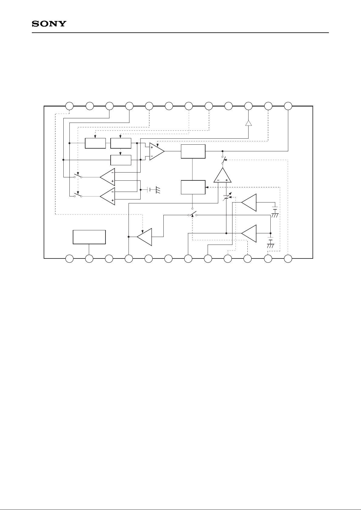
Block Diagram and Pin Configuration
BUF
VRT
DMSW1
9
10
11
12
13
1415
16
2
3
4
5
6
7
8
1
17
18
19
20
21
22
23
24
CDS
CLP1
AGC
SH3
DMSW2
CAM
SH
POWER
SAVE CONT
SH1 SH2
DC
SHIFT
VRT
DRV
V
RB
DRV
VRB
DRV
VREF
CDS
CLP2
AGC
CLP
OB SW
OFFSET
BLK SW
ICONT
V
CC
2
DIN
PIN
CLPDM
GND1
SHD
SHP
V
CC
1
CCDLEVEL
AGCCONT
AGCCLP
GND2
PS
GND3
DRVOUT
V
CC
3
N.C.
VRB
VRT
OFFSET
PBLK
XRS
CLPOB
– 3 –
CXA2096N
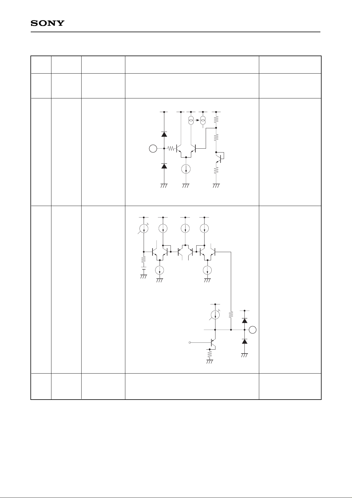
Pin Description (VCC1, 2, 3 = 3V)
2
PS
Power saving mode.
1
3
19
GND2
GND3
GND1
Ground.
VTH = 1.5V
GND
145
5k
10µA
2
1.5V
60k
30k
4
DRVOUT
Driver output for A/D
converter capable of
DC coupling.
Dynamic range =
1Vp-p.
VRB to
VRB + 100mV
5
16
23
VCC3
VCC1
VCC2
Power supply.VCC
CAM signal
48
50µA
145
ICONT
3.2 to 6.4mA
200µA
50µA
25µA25µA
2k
IOFFSET
0 to
50µA
VRB =
1.35V
4
Pin
No.
Symbol Pin voltage Equivalent circuit Description
– 4 –
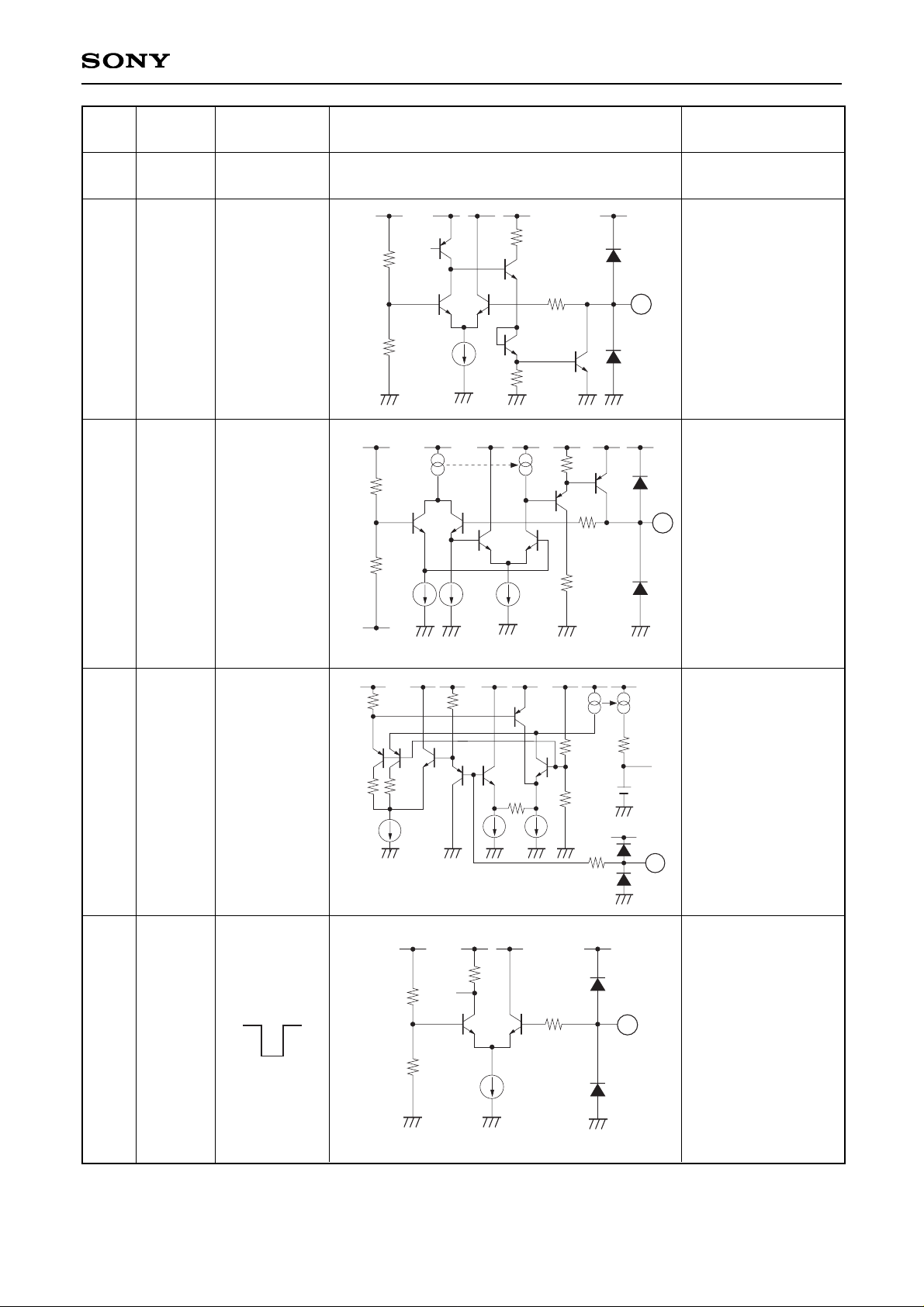
CXA2096N
7 VRB
1.35V regulator
output.
Be sure to decouple
this pin near the IC
pins to prevent the
oscillation and external
noise when this pin is
not used.
(Recommended
capacitor value: 4.7µF)
1.35V
2.35V8 VRT
2.35V regulator
output.
Be sure to decouple
this pin near the IC
pins to prevent the
oscillation and external
noise when this pin is
not used.
(Recommended
capacitor value: 4.7µF)
200
30k
16.5k
13.5k
145
1.35V
110µA
7
30k
6.5k
23.5k
145
2.35V
220µ
55µ
55µ
200
8
9 OFFSET
Controls the output
offset.
When 3V: VRB
When 1.5V: VRB +
100mV
When 0V (preset
mode): VRB + 35mV
1.5 to 3V
&
0V
2k
30k
30k
50k
50k
1.5k 3k
25k
VRB
145
50µA
50µA
50µA
1.85V
9
10 PBLK
Camera signal
preblanking pulse
input.
Active when Low.
Calibrates the black
level of the AGC
output waveform.
When PBLK is Low,
the DRVOUT
potential is forced to
VRB.
VTH = 1.85V
145
50µA
30k
30k
1.85V
30k
10
Active: Low
6 N.C.
No connection;
normally ground.
Pin
No.
Symbol Pin voltage Equivalent circuit Description
– 5 –
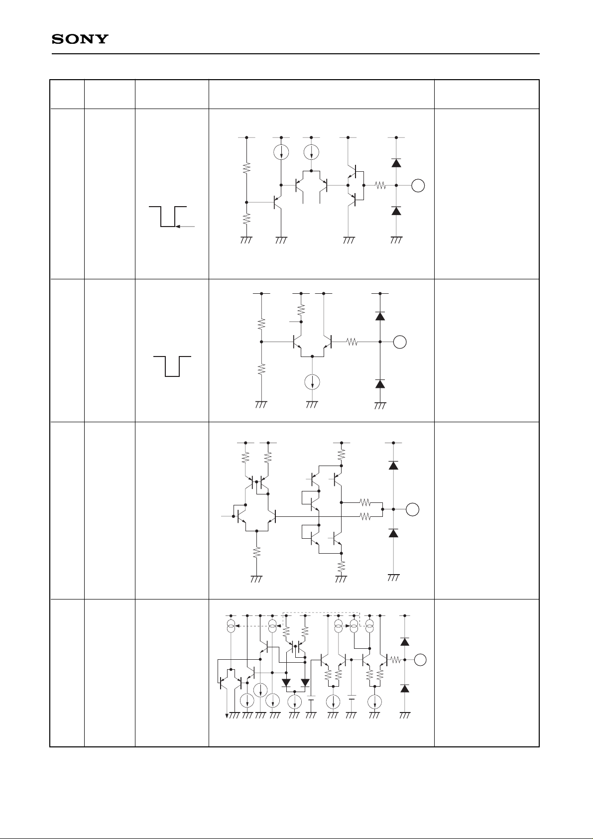
CXA2096N
11 XRS
Camera signal
sample-and-hold
pulse input.
VTH = 0.68V
24k
7k
0.68V
770µA
40µA
97µ
145
11
12 CLPOB
Clamp pulse used to
clamp the optical
black portion of the
camera signal after it
passes through the
AGC amplifier.
VTH = 1.5V
145
50µA
30k
30k
1.5V
30k
12
Sampling
Active: Low
13 AGCCLP
AGC clamp capacitor.
(Recommended
value: 0.1µF)
Approx. 1.3V
14
AGCCONT
AGC gain control.
When 1.5V: –1dB
(Minimum
gain)
When 3.0V: 31.5dB
(Maximum
gain)
1.5 to 3.0V
50k
145
145
5k5k
3k
3k
13
145
200µA
3.4k
3.4k
200µA
2.14V
100µA300µA
300µA 100µA
2.29V
ICONT
3.4k
3.4k
3.3k
3.3k
14
Pin
No.
Symbol Pin voltage Equivalent circuit Description
 Loading...