

Sony CXA2095S Datasheet
– 1 –
CXA2095S
E96X20-PS
Y/C/RGB/Sync/Deflection for Color TV
Description
The CXA2095S is a bipolar IC which integrates
the luminance signal processing, chroma signal
processing, RGB signal processing, and sync and
deflection signal processing functions for NTSC
system color TVs onto a single chip.
The following functions have been added to the
same function IC, CXA2025S.
1) Vertical sync pull-in speed switching function
2) YUV SW Y signal switching function
3) fsc output pin
Features
• I2C bus compatible
• Sync signal processing uses a countdown system
with non-adjusting H/V oscillator frequencies
• Built-in deflection compensation circuit capable of
supporting various wide modes
• Non-adjusting Y/C block filter
• Built-in AKB
• Video signal I/Os: Y/C separation input, Y/color
difference input, analog RGB input and RGB
output
• YUV SW Y signal switching function allows picture
quality adjustment for the Y signal in the same
manner as for the normal Y signal even when
Y/color difference input is selected
Applications
Color TVs (4:3, 16:9)
Structure
Bipolar silicon monolithic IC
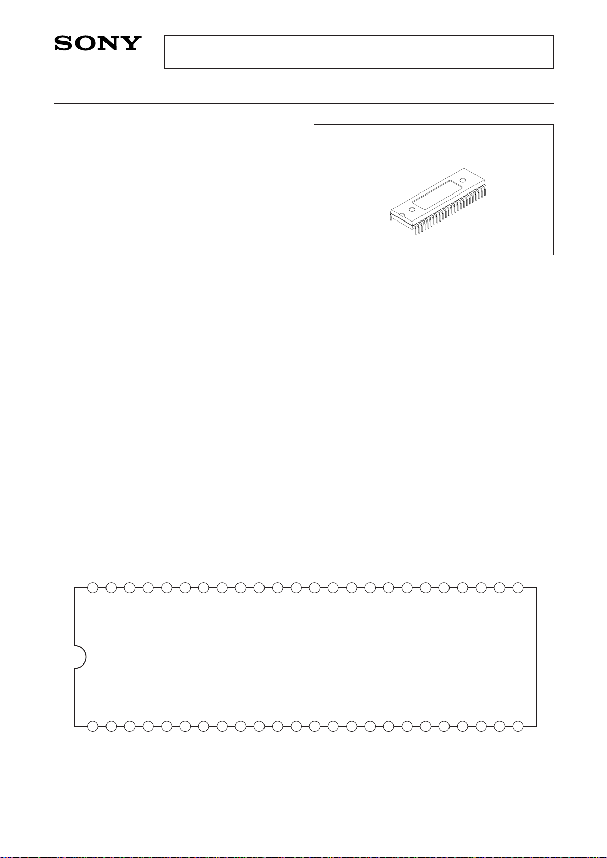
Pin Configuration
Absolute Maximum Ratings
(Ta = 25°C, SGND, JGND = 0V)
• Supply voltage SVCC, JVCC –0.3 to +12 V
• Operating temperature
Topr –20 to +75 °C
• Storage temperature
Tstg –65 to +150 °C
• Allowable power dissipation
PD 1.5 W
• Voltages at each pin –0.3 to SVCC, JVCC + 0.3 V
Operating Conditions
Supply voltage SVCC 9.0 ± 0.5 V
JVCC 9.0 ± 0.5 V
Sony reserves the right to change products and specifications without prior notice. This information does not convey any license by
any implication or otherwise under any patents or other right. Application circuits shown, if any, are typical examples illustrating the
operation of the devices. Sony cannot assume responsibility for any problems arising out of the use of these circuits.
48 pin SDIP (Plastic)
2
3
4
5
6
7
8
9
10
11
12
13
14
15
16
17
18
19
20
21
22
23
24
1
25
26
2728
29
30
40
39
38
37
35
34
31
32
33
41
42
43
44
45
46
47
48
36
BLHOLD
YIN
XTAL
APCFIL
CIN
SV
CC
YUV SW
EYIN
ERYIN
EBYIN
SGND
YM
YS
RIN
GIN
BIN
RSH
ROUT
GSH
GOUT
BSH
BOUT
SCL
SDA
VM
IKIN
ABLIN/VCOMP
ABLFIL
NC
FSCOUT
HSIN
VSIN
VSFIL
IREF
JGND
BGP
CERA
AFCFIL
L2FIL
AFCPIN/HOFF
HDRIVE
JV
CC
SAWOSC
VAGCSH
EWDRIVE
VDRIVE+/VPROT
VDRIVE–/VPROT
VTIM (SCP)
– 2 –
CXA2095S
I
2
C BUS
DECODER
D/A
IREF
VSYNC
SEP.
HSYNC
SEP.
PHASE
DETECTOR
32f
H VCO
H PHASE
DETECTOR
H DRIVE
H PHASE
SHIFTER
V SAW
OSC/AGC
V PARA
GEN.
V SAW
GEN.
WIDE
MODE
V ZOOMING
ABL
AXIS
Y/C MIX PICTURE
D-COL
GAMMA
CLAMP BRIGHT
DRIVE
AKB/CUTOFF/IK
BLANKING BUFFER
RGB CLAMP
YS SW
REF-P SW
YM ATT.
YUV SW
YUV
CLAMP
AMP
CHROMA
VCO
CHROMA
DEMOD.
KILLER
DETECTOR
COLOR
HUE
CHROMA
APC
TOT
ACC AMP
VM AMP
SUBCONT
C-TRAP
Y DELAY SHARPNESS
CLAMP
DC-TRAN
D-PIC
TIMING PULSE GEN.
V COUNT DOWN
1/32
DIVIDER
2
3
4
5
6
7
8
9
10
11
12
13
14
15
16
17
18
19
20
21
22
23
24
25
26 27
28
29
30
40
39
38
37
36
35
34
31
32
33
41 42
43
44
46
47
48
1
45
SDA
SCL
BGP
IREF
VSIN
VSFIL
HSIN
NC
AFCFIL
JGND
CERA
L2FIL
AFCPIN
/HOFF
HDRIVE
JV
CC
SAWOSC
VAGCSH
EWDRIVE
VDRIVE+
VDRIVE–
/VPROT
VTIM
ABLIN
/VCOMP
ABLFIL
IKIN
YIN
VM
BLHOLD
CIN
APCFIL
XTAL
SV
CC
YUVSW
EYIN
ERYIN
EBYIN
SGND
YM
YS
RIN
GIN
BIN
RSH
GSH
BSH
BOUT
GOUT
ROUT
FSCOUT
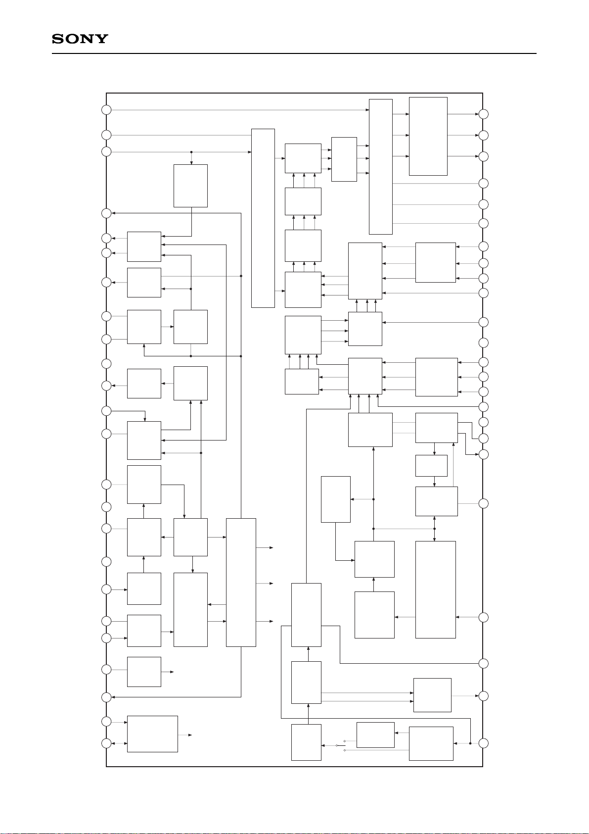
Block Diagram
– 3 –
CXA2095S
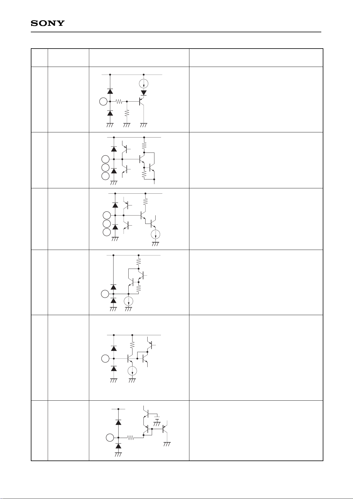
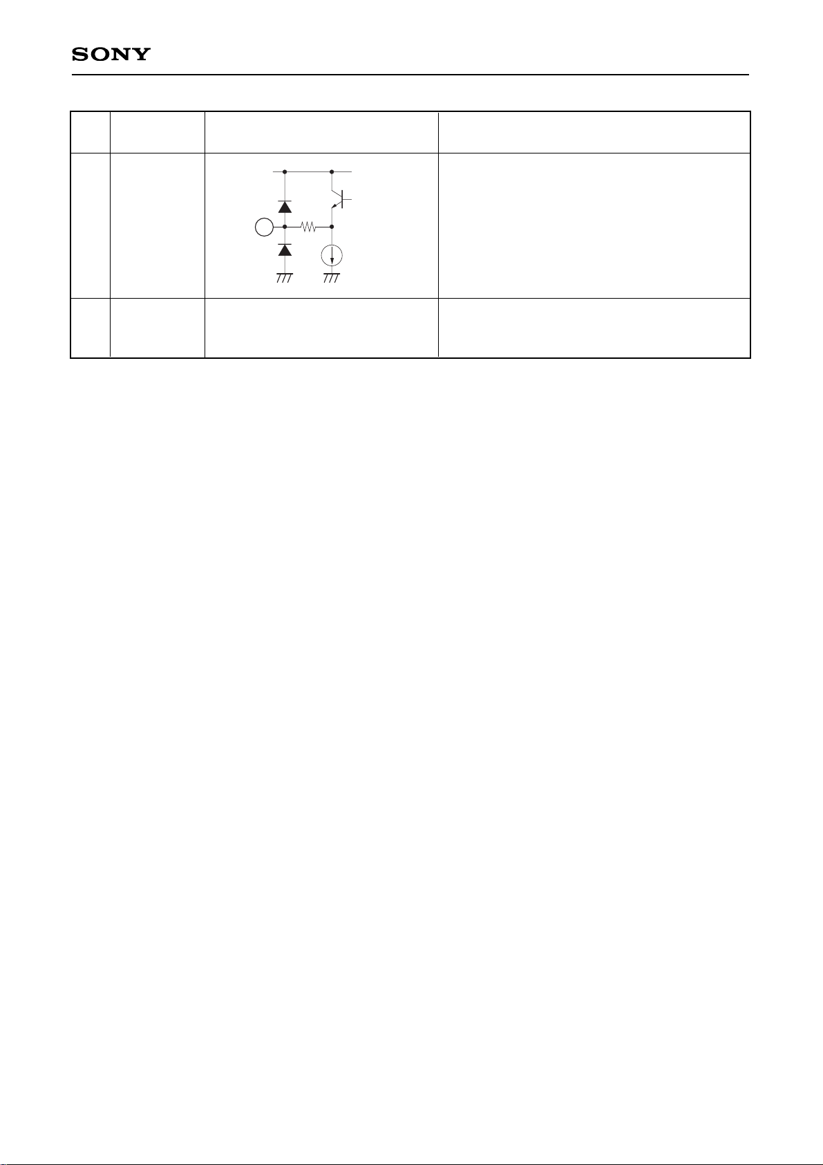
Pin Description
Pin
No.
Symbol Equivalent circuit Description
1
XTAL
Connect a 3.579545MHz crystal oscillator.
2
APCFIL
CR connection for the chroma APC lag-lead
filter.
3
BLHOLD
Capacitor connection for black peak hold of the
dynamic picture (black expansion).
4
YIN
Y signal input.
Input a 2Vp-p (including sync, 100% white) Y
signal via a capacitor. The pedestal level of the
input signal is clamped to 4.2V.
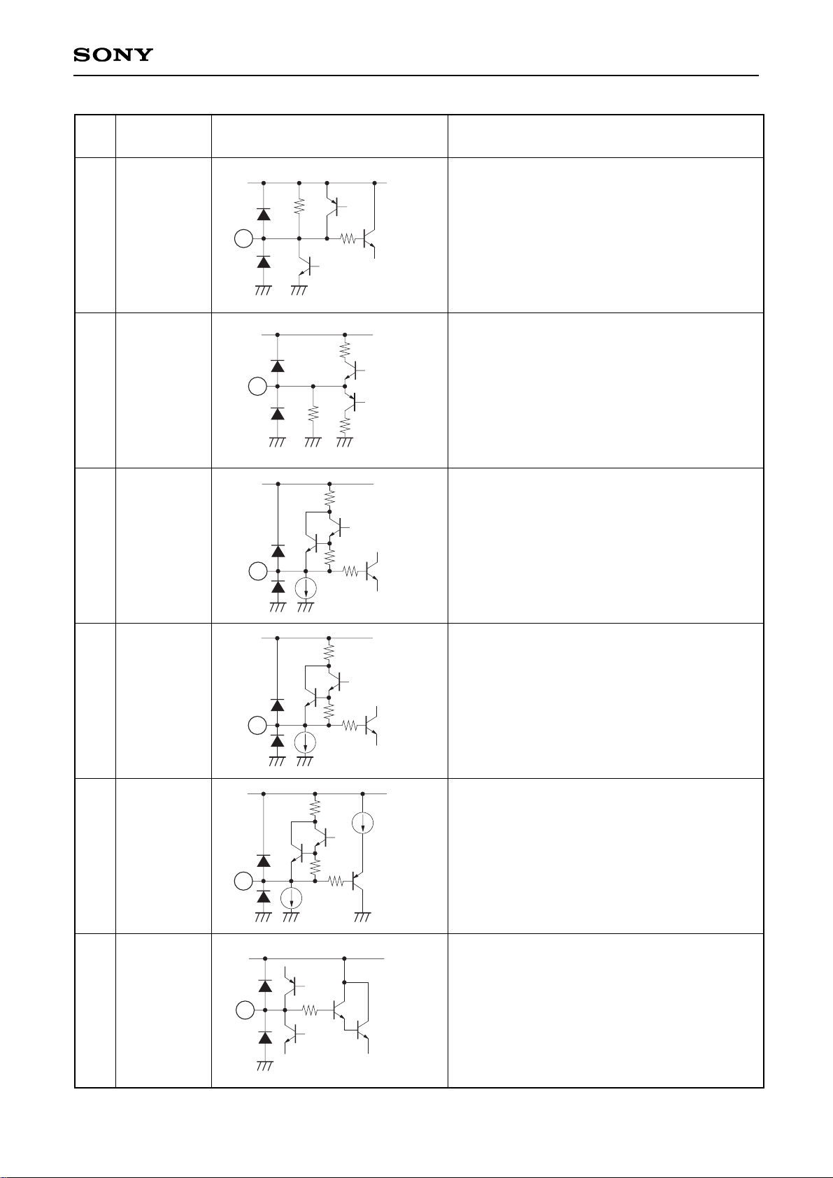
7 SCL
I2C bus protocol SCL (Serial Clock) input.
VILMAX = 1.5V
VIHMIN = 3.5V
350
SV
CC
1
200µ
2
1.2k
1.2k
SV
CC
50µ
50µ
1.2k
SVCC
3
20k
20k
4k
9µ
25µ
SVCC
1.2k
4
100µ
SVCC
30k
5
10p
35µ
4k
JVCC
7
10k
50µ
CIN
Chroma signal input.
Provide a bias of about VCC/2 and input a C
signal (including sync, 100% white, 2Vp-p CV
signal) with a 570mVp-p burst level.
Power supply for the video block.
5
6
SVCC
– 4 –
CXA2095S
8 SDA
I2C bus protocol SDA (Serial Data) I/O.
VILMAX = 1.5V
VIHMIN = 3.5V
VOLMAX = 0.4V
9
YUV SW
Switch control for the external YUV signal input.
When YUV SW is high, the external YUV signal
is selected; when YUV SW is low, the Y/C block
signal is selected. However, when the EY-SW
register is 1, the YIN (Pin 4) input is selected for
the Y signal even if YUV SW is high.
VILMAX = 0.4V
VIHMIN = 1.0V
VIHMAX = 3.0V
10
EYIN
External Y signal input.
Input a 0.7Vp-p (100 IRE) Y signal via a
capacitor. The signal is clamped to 6.5V at the
burst timing of the signal input to the sync input
(Pin 44).
11
ERYIN
External R-Y signal input.
Input a 0.78Vp-p (color difference signal
obtained by detecting a 100 IRE, 0.7Vp-p,
100% color bar chroma signal at the orthogonal
axis) + (R-Y) signal via a capacitor. The signal
is clamped to 6.2V at the burst timing of the
signal input to the sync input (Pin 44).
14
YM
YM switch control input.
When YM is high, the Y/C block signal is
attenuated by 6dB.
VILMAX = 0.4V
VIHMIN = 1.0V
VIHMAX = 3.0V
JVCC
8
50µ
SVCC
147
40k
9
100µ
11
12
SVCC
1k
40k
10
2k
SVCC
147
14
40k
100µ
12
EBYIN
External B-Y signal input.
Input a 1.0Vp-p (color difference signal obtained
by detecting a 100 IRE, 0.7Vp-p, 100% color
bar chroma signal at the orthogonal axis) + (BY) signal via a capacitor. The signal is clamped
to 6.2V at the burst timing of the signal input to
the sync input (Pin 44).
GND for the video block.
13
SGND
Pin
No.
Symbol Equivalent circuit Description
– 5 –
CXA2095S
15
YS
YS switch control input.
When YS is high, the RGB block signal is
selected; when YS is low, the Y/C block is
selected.
VILMAX = 0.4V
VIHMIN = 1.0V
VIHMAX = 3.0V
16
17
18
RIN
GIN
BIN
Analog R, G and B signal input.
Input a 0.7Vp-p (no sync, 100 IRE) signal via a
capacitor. The signal is clamped to 5.1V at the
burst timing of the signal input to the sync input
(Pin 44).
19
21
23
RSH
GSH
BSH
Sample-and-hold for R, G and B AKB.
Connect to GND via a capacitor. When not using
AKB (manual cut-off mode), R, G and B cut-off
voltage can be controlled by applying a control
voltage to each pin. The control voltage is 4.2 ±
2V.
20
22
24
ROUT
GOUT
BOUT
R, G and B signal output.
2.4Vp-p is output during 100% white input.
26
ABLIN
/VCOMP
ABL control signal input and VSAW high voltage
fluctuation compensation signal input.
High voltage compensation has linear control
characteristics for the pin voltage range of about
8V to 1V.
ABL operates when the pin voltage becomes
lower than about 1.2V.
SVCC
147
40k
15
100µ
17
18
SVCC
30k
200
16
21
23
SVCC
1k
19
50µ
12k
200
SVCC
20
1100µ
SVCC
1k
25
50µ
SVCC
147
26
25
IKIN
Input the signal converted from the CRT beam
current (cathode current IK) to a voltage via a
capacitor. The V blanking part is clamped to 2.7V at
the V retrace timing.
The input for this pin is the reference pulse return,
and the loop operates so that the Rch, the Gch and
Bch are all 1Vp-p. (∗For the CXA2025S, the loop
operates so that the Rch is 1Vp-p and the Gch and
Bch are 0.83Vp-p.) The Gch and Bch can be varied
by ±0.5V by the bus CUTOFF control. When not
using AKB, this pin should not be connected.
Pin
No.
Symbol Equivalent circuit Description
– 6 –
CXA2095S
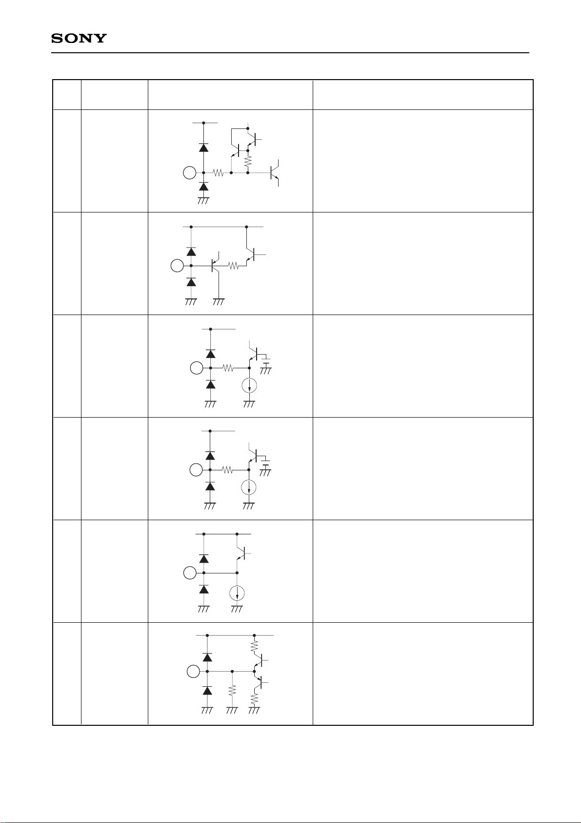
27
ABLFIL
Connect a capacitor to form the LPF of the ABL
control signal.
28
VTIM
(SCP)
V timing pulse output.
Outputs the timing pulse from V sync
identification to the end of V blanking. Pulses are
positive polarity from 0 to 6 [V]. During zoom
mode, the V blanking pulse which has been
expanded before and after the V sync is
superimposed and output as the 0 to 3 [V] pulse.
29
VDRIVE–
/VPROT
V sawtooth wave output and Vprotect signal
input.
When a large current (3mA) is led from this pin,
the RGB outputs are all blanked and the status
is returned to the I2C bus.
30
VDRIVE+
/VPROT
Outputs a V sawtooth wave of the opposite
polarity as VDRIVE–. The Vprotect function can
also be operated by this pin.
32
VAGCSH
Sample-and-hold for AGC which maintains the V
sawtooth wave at a constant amplitude.
Connect to GND via a capacitor.
SVCC
10k
1.2k
27
JVCC
1k
28
10k
1k
JVCC
30k
29
24k
720
400µ
JVCC
30k
24k
720
30
400µ
JVCC
15k
78k
1.4k
31
25µ
800µ
JVCC
32
1.2k
31
EWDRIVE
V parabola wave output.
Pin
No.
Symbol Equivalent circuit Description
– 7 –
CXA2095S
33
SAWOSC
Connect a capacitor to generate the V sawtooth
wave.
35
HDRIVE
H drive signal output.
This signal is output with the open collector.
This pin goes high (OFF) during hold-down.
∗
For the CXA2025S, this pin is low (ON) during
hold-down.
36
AFCPIN
/HOFF
H deflection pulse input for H AFC.
Input an about 5Vp-p pulse via a capacitor. Set
the pulse width to 10 to 12µs. This pin is also
used as the hold-down signal input for the HD
output, and if this pin is 1 [V] or less for a 7V
cycle or longer, the hold-down function operates
and the HD output goes to high (OFF).
In addition, the RGB outputs are all blanked and
the status is returned to the I2C bus.
37
L2FIL
Filter for H AFC.
Connect to GND via a capacitor. The H phase
can also be controlled from this pin by leading
current in and out of this capacitor.
As the pin voltage rises, the picture shifts to the
left; as the pin voltage drops, the picture shifts to
the right.
39
CERA
Connect the ×32fH VCO ceramic oscillator.
JVCC
100
33
100
100µ
JVCC
35
147
20k
JVCC
147
10k
10k
60k
36
50µ 50µ
4.2V
JVCC
100
37
25µ
JVCC
1.2k
38
46k
50µ
50µ
10k
JVCC
39
400µ
50µ
38
AFCFIL
CR connection for the AFC lag-lead filter.
40
JGND
GND for the deflection block.
34
JVCC
Power supply for the deflection block.
Pin
No.
Symbol Equivalent circuit Description
– 8 –
CXA2095S
41
IREF
Internal reference current setting.
Connect to GND via a 15kΩ resistor.
42
VSFIL
Filter for V sync separation.
Connect to GND via a capacitor.
43
VSIN
Sync signal input for V sync separation.
Input a 2Vp-p Y signal.
44
HSIN
Sync signal input for H sync separation.
Input a 2Vp-p Y signal.
46
BGP
Burst gate pulse output.
This pulse is a 0 to 3V positive polarity pulse.
While this pulse is gated near V-Sync for the
CXA2025S, it is constantly output for the
CXA2095S.
20k
JVCC
147
41
JVCC
1k
42
JVCC
147
43
20µ
JVCC
147
44
10µ
SVCC
45
400µ
1k
15k
1k
46
45
VM
Y signal differential waveform output for VM
(Velocity Modulation). (7.1VDC, 2.0Vp-p) The
signal delayed for 250ns from YIN is output.
The delay time from YIN and the differential
coefficient of the output signal vary according to
sharpness f0 control.
Pin
No.
Symbol Equivalent circuit Description
– 9 –
CXA2095S
47
FSCOUT
Sub carrier output.
Output level: 5.9VDC, 0.5Vp-p
48
NC
This pin is not connected.
Connect to GND normally to prevent interference
to others.
SVCC
300µ
47
147
Pin
No.
Symbol Equivalent circuit Description
– 10 –
CXA2095S
Electrical Characteristics
Setting conditions
• Ta = 25°C, SVCC = JVCC = 9V, SGND = JGND = 0V
• Measures the following after setting the I
2
C bus register as shown in “I
2
C bus register initial settings”.
No.
Item Symbol Measurement conditions
Measure-
ment pin
Measurement contents
Min. Typ. Max. Unit
No.
Item Symbol Measurement conditions
Measure-
ment pin
Measurement contents
Min. Typ. Max. Unit
1
Signal block current
consumption
SI
CC
SVCC = 9.0V,
Bus data = center
6
Measure the pin inflow current.
40
65 90
mA
2
Sync block current
consumption
JI
CC
JVCC = 9.0V,
Bus data = center
34
Measure the pin inflow current.
25
45
60
mA
3
Horizontal free-running
frequency
fHFR
AFC MODE = 0H
35
HDRIVE output frequency
Confirm that I
2
C status register HLOCK is 1
(the pull-in range when f
H is shifted from 15.734kHz).
Measure the pulse width for the section where the
HDRIVE output is high.
Measure the pulse width for the section where the BGP
output is high.
Measure the VDRIVE output Vp-p.
15.55
15.734
15.9
kHz
4
Horizontal sync pull-in
range
∆
f
HR
SYNC IN: composite sync
—
–400
—
400
Hz
5 HD output pulse width
HDw
SYNC IN: composite sync
35
24.5
25.5
26.5
µs
6 BGP output pulse width
VBGPh
46
3.1 4.0
4.9
µs
7
VDRIVE output
amplitude
VSpp
SYNC IN: composite sync
29,
30
0.8
0.95 1.1
V
8
VDRIVE output center
potential
VSdc
29,
30
2.9
3.0
3.15
V
Sync deflection block items
VSpp
43: VSIN in
VSdc
8.97ms
VDRIVE+
– 11 –
CXA2095S
9
EWDRIVE output
amplitude
VEWpp
SYNC IN: composite sync
31
Measure the EWDRIVE output Vp-p.
0.5
0.65
0.8
V
10
EWDRIVE output center
potential
VEWdc
31
3.7
4.0
4.2
V
VEWpp
43: VSIN in
8.97ms
11
R, G and B output
amplitude
VRout1
20,
22,
24
Output amplitude when a video signal with an amplitude
of 1.4Vp-p/100 IRE is input
2.1
2.4
2.7
V
Signal block items
12
R, G and B output
linearity
Lin
20,
22,
24
95
100
105
%
13 C-TRAP attenuation
C-Trap
C-TRAP = 0/1
CTRAP-ADJ = 7H
20
—
–37.5
—
dB
1.4Vp-p/100 IRE
YIN:
100 IRE
50 IRE
YIN:
YIN:
fsc, 50 IRE
Lin = × 100
V1
V2
V1
V2 × 2
f = 3.58MHz
No.
Item Symbol Measurement conditions
Measure-
ment pin
Measurement contents Min. Typ. Max. Unit
No.
Item Symbol Measurement conditions
Measure-
ment pin
Measurement contents
Min. Typ. Max. Unit
Input fsc to YIN.
Ratio of the fsc component of the Rout amplitude when
CTRAP=1 against the Rout amplitude when CTRAP=0.
– 12 –
CXA2095S
14
15
16
17
18
19
20
21
VM output
Color gain
Hue center offset
Killer point
APC pull-in range
Dynamic color operation
R output
Dynamic color operation
B output
YM gain
Vvm
Vcol
φoffset
KP
∆f
APC
∆GdcolR
∆GdcolB
∆GYM
45
24
—
—
—
20
24
20,
22,
24
Confirm that status register KILLER is 1 when the burst
level is –31dB assuming burst 570mVp-p to be 0dB.
Confirm that the burst frequency is pulled in at 3.58MHz
±400Hz.
∆GdcolR = × 100
∆GdcolB = × 100
Output amplitude ratio of the R, G and BOUT when YM
is high and low
Vpp (DCOL = 1)
Vpp (DCOL = 0)
ROUT, BOUT
1.5
2.2
2.4
V
0.75
0.98
1.2
V
–8.5 0 8.5 deg
— –31 — dB
–400 — 400 Hz
YIN: 100 IRE
D-COL = 0/1
SUBCONT = F
50 IRE
f = 3MHz
Vvm
YIN
VM
CIN
180° 0°
500mVpp
Vpp
BOUT
Vpp
YIN: 3MHz, 50 IRE
VM = 1
YIN: GND
CIN: burst
+180°, 500mVp-p
COLOR = 1F
HUE = 1F, SUB-HUE = 7
YIN = GND
CIN: burst only
94
96
98
%
104
106
108
%
–7.1
–6.1
–5.1
dB
Vpp (DCOL = 1)
Vpp (DCOL = 0)
No.
Item Symbol Measurement conditions
Measure-
ment pin
Measurement contents Min. Typ. Max. Unit
 Loading...