

Sony CXA2093S Datasheet
Sharpness for Display
Description
The CXA2093S is a bipolar IC which performs
contour accentuation for display RGB signals.
Features
• Sharpness time constant selection (50ns/100ns)
• Built-in sync separator for sync on green
• Differential output pins
• Built-in wide-band amplifier (200MHz/–3dB@0.7Vp-p)
Applications
Display
Structure
Bipolar silicon monolithic IC
Absolute Maximum Ratings (Ta = 25°C, GND = 0V)
• Supply voltage VCC 7V
• Operating temperature Topr –20 to +75 °C
• Storage temperature Tstg –65 to +150 °C
• Allowable power dissipation PD 1.13 W
Operating Conditions
Supply voltage VCC 5 ± 0.25 V
– 1 –
E97680A26-PS
Sony reserves the right to change products and specifications without prior notice. This information does not convey any license by
any implication or otherwise under any patents or other right. Application circuits shown, if any, are typical examples illustrating the
operation of the devices. Sony cannot assume responsibility for any problems arising out of the use of these circuits.
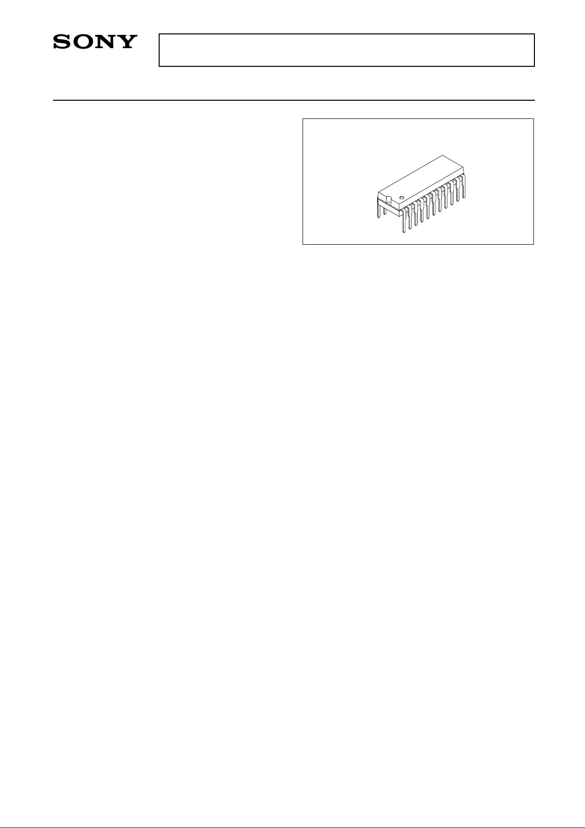
CXA2093S
22 pin SDIP (Plastic)

– 2 –
CXA2093S
Block Diagram
Pin Configuration
3
5
7
14
15
17
19
21
1
RIN
GIN
BIN
SYNCIN
DIFOUT
ROUT
GOUT
BOUT
SYNCOUT
CLAMP
Limiter
Limiter level = 30%
Y operation
1st-order
differential
(100ns)
1st-order
differential
(50ns)
GCA
Time constant
selection
Switching
identification
SyncSep
12
f0/GAIN
GAIN Min. GAIN Max.
0.5V to 2.0V ; 50ns
3.0V to 4.5V ; 100ns
13
CLAMP
VILMAX = 0.8V
VIHMIN = 2.8V
Y = 0.6G + 0.3R + 0.1B
2
3
4
5
6
7
8
9
10
11
12
13
14
15
16
17
18
19
20
21
22
1
GND
ROUT
GND
GOUT
V
CC
BOUT
VCC
DIFOUT
SYNCOUT
CLAMP
F0_GAIN
RIN
GND
GND
BIN
V
CC
SYNCIN
GND
NC
GND
NC
GIN
– 3 –
CXA2093S
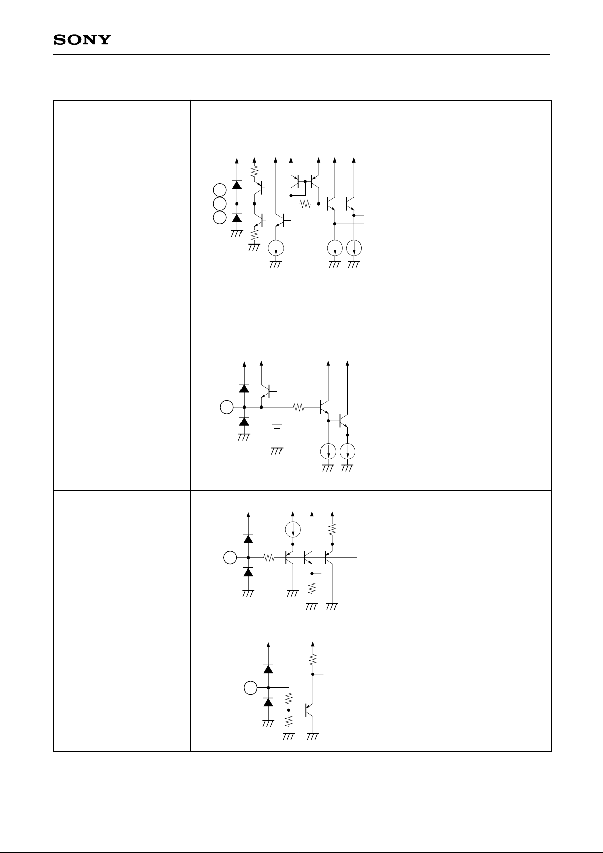
Pin Description
Pin
No.
1
3
5
RIN
GIN
BIN
RGB input pins.
Input these pins through
capacitor.
Symbol
Pin
voltage
Equivalent circuit Description
5
1
3
VCC VCC VCC VCC VCC VCC VCC
250
500
150
7
SYNCIN
Sync input pin for sync on green.
Input this pin through capacitor.
7
VCC VCC VCC VCC
150
100µA
2, 4
8, 10
20, 22
GND
GND pins.
12
F0_GAIN
Sharpness time constant
selection and gain control pin.
VCC VCC VCC
143
12
30k
30k
13
CLAMP
Clamp pulse input pin.
ILMAX; 0.8V
IHMIN; 2.8V
VCC VCC
50k
30k
20k
13

– 4 –
CXA2093S
19
21
23
BOUT
GOUT
ROUT
RGB signal output pins.
19
21
23
VCC VCC VCC
6mA
625
1p
6, 16
18, 20
V
CC
Power supply pins.
14
SYNCOUT
Sync output pin.
0 to 4.3V positive polarity pulse is
output in synchronizing with sync.
VCC VCC
150
14
VCC VCC
15
DIFOUT
Differential signal output pin.
VCC VCC
15
VCC
2mA
625
1p
5V
(applied)
Pin
No.
Symbol
Pin
voltage
Equivalent circuit Description
 Loading...