

Sony CXA2089S, CXA2089Q Datasheet
Description
The CXA2089Q/S is a 5-input, 2-output audio/video
switch featuring I2C bus compatibility for TVs. This IC
has input pins that are compatible with S2 protocol.
Features
• 3 inputs that are compatible with S2 protocol
• Serial control with I2C bus
• 5 inputs, 2 outputs
• The desired inputs can be selected independently
for each of the 2 outputs
• Wide band video amplifier (20MHz, –3dB)
• Y/C MIX circuit
• Slave address can be changed (90H/92H)
• Audio muting from external pin
• High impedance maintained by I2C bus lines (SDA,
SCL) even when power is OFF
• Wide audio dynamic range (3Vrms typ.)
Applications
Audio/video switch featuring I2C bus compatibility
for TVs
Structure
Bipolar silicon monolithic IC
Absolute Maximum Ratings
• Supply voltage VCC 12 V
• Operating temperature Topr –20 to +75 °C
• Storage temperature Tstg –65 to +150 °C
• Allowable power dissipation
PD 1500 mW
Operating Conditions
Supply voltage 9 ± 0.5 V
– 1 –
CXA2089Q/S
E97431B7Z-PS
S2-Compatible 5-Input 2-Output Audio/Video Switch
Sony reserves the right to change products and specifications without prior notice. This information does not convey any license by
any implication or otherwise under any patents or other right. Application circuits shown, if any, are typical examples illustrating the
operation of the devices. Sony cannot assume responsibility for any problems arising out of the use of these circuits.
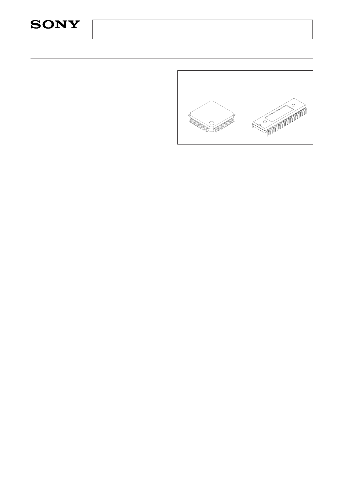
CXA2089Q
48 pin QFP (Plastic)
CXA2089S
48 pin SDIP (Plastic)
– 2 –
CXA2089Q/S
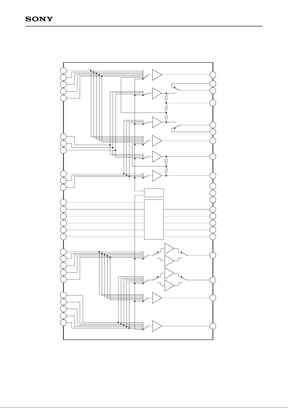
Block Diagram
CXA2089Q
47
VOUT1
YOUT1
TV
V4
V3
V2
V1
Y3
Y2
Y1
C3
C2
C1
YIN1
TRAP1
GND
COUT1
CIN1
VOUT2
YOUT2
COUT2
BIAS
V
CC
6dB
6dB
6dB
6dB
6dB
6dB
BIAS
40
38
37
42
43
44
45
ADR
SDA
SCL
DC OUT
MUTE
Logic
27
28
36
34
33
8
15
1
3
5
10
12
17
19
26
23
32
S-3
S2-1
LTV
LV4
S-2
S-1
S2-3
S2-2
LV3
LV2
LV1
LOUT1
ROUT1
LOUT2
ROUT2
6dB
0dB
6dB
0dB
6dB
6dB
39
41
30
22
2
9
16
6
7
13
14
20
21
46
RTV
RV4
RV3
RV2
RV1
31
29
48
4
11
18
24
35
25
Audio system is attenuated by 6dB for 6kΩ resistor input, and a total gain is 0dB (LOUT1 and ROUT1 can be changed to –6dB).

– 3 –
CXA2089Q/S
CXA2089S
VOUT1
YOUT1
TV
V4
V3
V2
V1
Y3
Y2
Y1
C3
C2
C1
YIN1
TRAP1
GND
COUT1
CIN1
VOUT2
YOUT2
COUT2
BIAS
V
CC
6dB
6dB
6dB
6dB
6dB
6dB
BIAS
ADR
SDA
SCL
DC OUT
MUTE
Logic
S-3
S2-1
LTV
LV4
S-2
S-1
S2-3
S2-2
LV3
LV2
LV1
LOUT1
ROUT1
LOUT2
ROUT2
6dB
0dB
6dB
0dB
6dB
6dB
RTV
RV4
RV3
RV2
RV1
5
7
14
21
29
9
16
23
11
18
25
12
19
26
13
20
27
4
8
15
22
28
6
10
17
24
30
46
42
1
48
3
44
39
37
35
2
43
34
32
33
31
41
40
45
47
36
38
Audio system is attenuated by 6dB for 6kΩ resistor input, and a total gain is 0dB (LOUT1 and ROUT1 can be changed to –6dB).
13
14
15
16
17
18
19
20
21
22
23
24
25
26
27
28
29
30
36
35
34
31
32
33
40
39
38
37
41
42
43
44
45
46
47
48
2
3
4
5
6
7
8
9
10
11
121
BIAS
CIN1
LOUT1
VOUT1
ROUT1
TRAP1
YOUT1
GND
COUT1
LTV
TV
RTV
RV4
V4
LV4
S-3
S2-3
C3
RV3
Y3
LV3
V3
S-2
S2-2
YIN1
MUTE
V
CC
VOUT2
ROUT2
YOUT2
LOUT2
COUT2
DC OUT
SDA
SCL
ADR
V1
LV1
Y1
RV1
C1
S2-1
S-1
V2
LV2
Y2
RV2
C2
– 4 –
CXA2089Q/S
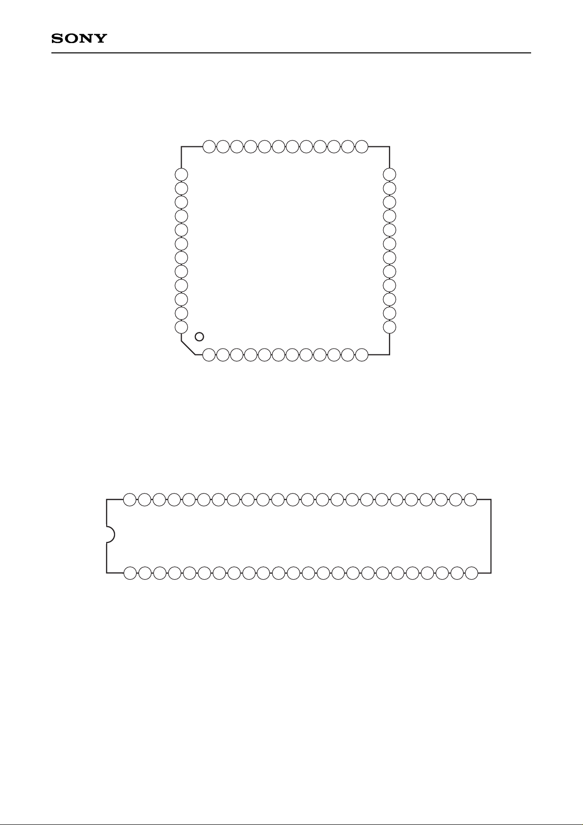
Pin Configuration
CXA2089Q
13
14 15
16
17
18
19
20
21
22
23
24
25
26
27
28
29
30
36
35
34
31
32
33
40
39
38
37
41
42
43
44
45
46
47
48
2
3
4
5
6
7
8
9
10
11
121
BIAS
CIN1
LOUT1
VOUT1
ROUT1
TRAP1
YOUT1
GND
COUT1
LTV
TV
RTV
RV4
V4
LV4
S-3
S2-3
C3
RV3
Y3
LV3
V3
S-2
S2-2
YIN1
MUTE
V
CC
VOUT2
ROUT2
YOUT2
LOUT2
COUT2
DC OUT
SDA
SCL
ADR
V1
LV1
Y1
RV1
C1
S2-1
S-1
V2
LV2
Y2
RV2
C2
CXA2089S
– 5 –
CXA2089Q/S
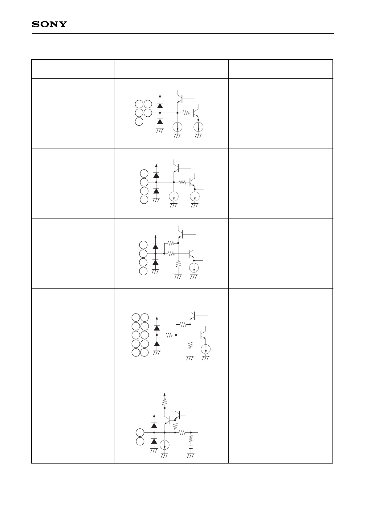
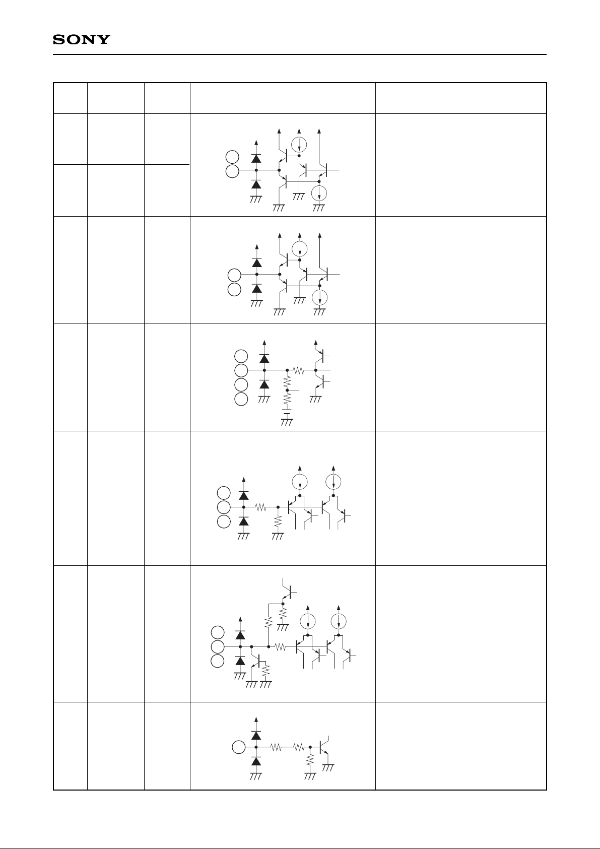
Pin Description Pin numbers in brackets are for the CXA2089S.
Pin
No.
47 (5)
1 (7)
8 (14)
15 (21)
23 (29)
TV
V1
V2
V3
V4
4.0V
Video signal inputs.
Input composite video signals.
Symbol
Pin
voltage
Equivalent circuit Description
150
VCC
3µA
47
1
15
23
8
3 (9)
10 (16)
17 (23)
36 (42)
Y1
Y2
Y3
YIN1
4.0V
Y/C separation signal inputs.
Input luminance signals.
The YIN1 pin inputs the signal
obtained by Y/C separating the
VOUT1 pin output.
3
10
17
150
VCC
3µA
36
5 (11)
12 (18)
19 (25)
38 (44)
C1
C2
C3
CIN1
4.5V
Y/C separation signal inputs.
Input chrominance signals.
The CIN1 pin inputs the signal
obtained by Y/C separating the
VOUT1 pin output.
150
V
CC
27k
20k
5
12
19
38
46 (4)
2 (8)
9 (15)
16 (22)
22 (28)
48 (6)
4 (10)
11 (17)
18 (24)
24 (30)
LTV
LV1
LV2
LV3
LV4
RTV
RV1
RV2
RV3
RV4
4.5V Audio signal inputs.
VCC
15k
33k
27k
2
4
9
11
16
18
46
48
22
24
40 (46)
33 (39)
VOUT1
VOUT2
3.9V
Video signal outputs.
Output composite video signals.
VCC
27k
VCC
23.5k
30k
250
40
33
– 6 –
CXA2089Q/S
45 (3)
29 (35)
COUT1
COUT2
4.5V
Video signal outputs.
Output chrominance signals.
VCC
VCC VCC VCC
45
29
43 (1)
YOUT1
3.3V
31 (37)
YOUT2
3.5V
Video signal outputs.
Output luminance signals.
VCC
VCC VCC VCC
43
31
39 (45)
30 (36)
41 (47)
32 (38)
LOUT1
LOUT2
ROUT1
ROUT2
4.5V
Audio signal outputs.
Zo = 50Ω (within DC ± 2mA)
VCC
VCCVCC
147
100k
6
13
20
6 (12)
13 (19)
20 (26)
S2-1
S2-2
S2-3
—
Detects the S2-compatible DC
superimposed onto the C signal.
4:3 video signal at 1.3V or less
4:3 letter-box signal at 1.3V or more
to 2.5V or less
16:9 picture squeezed signal at 2.5V
or more
These pins are pulled down to GND
by a 100kΩ resistor, so the 4:3 video
signals are selected when open.
VCC VCC
20k
56
20k
39
30
41
32
7 (13)
14 (20)
21 (27)
S-1
S-2
S-3
—
Composite video/S selector.
The detection results are written to
the status register.
S signal at 3.5V or less
Composite video signal at 3.5V or
more
These pins are pulled up to 5V by a
100kΩ resistor, so the composite
video signals are selected when
open.
VCC
VCCVCC
50k
10k
100k
50k
5V
7
14
21
25 (31)
ADR —
Selects the slave address for the I2C
bus.
90H at 1.5V or less
92H at 2.5V or more
90H when open
VCC
147
28k
72k
25
Pin
No.
Symbol
Pin
voltage
Equivalent circuit Description

– 7 –
CXA2089Q/S
27 (33)
SDA
—
I2C bus signal input
VILmax = 1.5V
VIHmin = 3.0V
VOLmax = 0.4V
VCC
4k
27
26 (32)
SCL
—
I2C bus signal input
VILmax = 1.5V
VIHmin = 3.0V
VCC
4k
10k
26
28 (34)
DC OUT —
Outputs the S2-compatible DC
superimposed onto the COUT2
output. The DC is superimposed by
connecting this pin to the COUT2
output via a capacitor.
Control is performed by the I2C bus.
When 0V is output, Q1 is ON and
the impedance is 5kΩ.
S2 protocol output DC impedance of
10 ± 3kΩ is realized by attaching
external resistance of 4.7kΩ.
DC OUT (bus) Output DC
0 4.5V
1 0V
2 1.9V
3 4.5V
VCC
100
1k
42
42 (48)
TRAP1 3.8V
Connects trap circuit for subcarrier.
VCC
4k
28k
1k
Q1
28
35 (41)
MUTE —
Audio signal output mute.
Mute OFF at 1.5V or less
Mute ON at 2.5V or more
Mute OFF when open
VCC
147
28k
72k
35
37 (43)
BIAS 4.5V
Internal reference bias (Vcc/2).
Connects to GND via a capacitor.
VCC
VCC
147
20k
VCC
20k
37
Pin
No.
Symbol
Pin
voltage
Equivalent circuit Description
– 8 –
CXA2089Q/S
Electrical Characteristics (Ta = 25°C, VCC = 9V)
Item
Current consumption ICC No signal, no load 30 45 62 mA
Symbol Conditions Min. Typ. Max. Unit
Video system (Measurement circuit; Fig. 1)
Gain
Frequency response
characteristics
Frequency response
characteristics
(Y/C mix)
Input dynamic range
Cross talk
GVv
FBWv1
FBWv2
Ddv
Vctv
f = 100kHz, 0.3Vp-p input
f = 100kHz, input frequency where
output amplitude is –3dB with 0.3Vp-p
output serving as 0dB
f = 100kHz,
maximum with distortion < 1.0%
f = 4.43MHz, 1Vp-p input
5.9
15
10
1.4
—
6.4
20
15
—
—
6.9
—
—
—
–50
dB
MHz
MHz
Vp-p
dB
Audio system (Measurement circuits; Fig. 2 to Fig. 5)
Gain
Frequency response
characteristics
Total harmonic
distortion
Input dynamic range
Cross talk
Ripple rejection ratio
Output DC offset
Residual noise
S/N ratio
GVA
FBWA
THD
DdA
VctA
VctA
Voff
VNA
S/N
f = 1kHz, 1Vp-p input,
5.7kΩ resistor inserted to input
f = 1kHz, input frequency where
output amplitude is –3dB with 1Vp-p
output serving as 0dB
f=1kHz, 2.2Vp-p input, where 400Hz
HPF + 80kHz LPF are inserted
f=1kHz, maximum with distortion < 0.3%
f=1kHz, 1Vp-p input
f=100Hz, 0.3Vp-p applied to Vcc
Offset voltage between input and
output
When 400Hz HPF+ 30kHz LPF are
inserted
f=1kHz, 1Vrms input
When 400Hz HPF + 30kHz LPF are
inserted
–1
50
—
2.8
—
—
–30
0
0
—
0.03
3.0
–90
–55
—
20
–100
1
—
0.05
—
–80
–40
30
30
–90
dB
kHz
%
Vrms
dB
dB
mV
µVrms
dB
– 9 –
CXA2089Q/S
High level input voltage
Low level input voltage
Low level output voltage
High level input current
Low level input current
Maximum clock
frequency
Minimum waiting time
for data change
Minimum waiting time
for data transfer start
Low level clock pulse
width
High level clock pulse
width
Minimum waiting time
for start preparation
Minimum data hold time
Minimum data
preparation time
Rise time
Fall time
Minimum waiting time
for stop preparation
VIH
VIL
VOL
IIH
IIL
fSCL
tBUF
tHD;STA
tLOW
tHIGH
tSU;STA
tHD;DAT
tSU;DAT
tR
tF
tSU;STO
With SDA 3mA current supplied
VIH = 4.5V
VIL = 0.4V
3.0
0
0
0
0
0
4.7
4.0
4.7
4.0
4.7
150
0
—
—
4.7
—
—
—
—
—
—
—
—
—
—
—
—
—
—
—
—
5.0
1.5
0.4
10
10
100
—
—
—
—
—
—
—
1
300
—
V
V
V
µA
µA
kHz
µs
µs
µs
µs
µs
ns
ns
µs
ns
µs
Logic system
Item Symbol Conditions Min. Typ. Max. Unit
 Loading...