

Sony CXA2079Q Datasheet

Description
The CXA2079Q is a 6-input, 2-output audio/video
switch featuring I2C bus compatibility for TVs. This IC
has input pins that are compatible with S2 protocol.
Features
• 4 inputs that are compatible with S2 protocol
• Serial control with I2C bus
• 6 inputs, 2 outputs
• The desired inputs can be selected independently
for each of the 2 outputs
• Wide band video amplifier (20MHz, –3dB)
• Y/C MIX circuit
• Slave address can be changed (90H/92H)
• Audio muting from external pin
• High impedance maintained by I2C bus lines (SDA,
SCL) even when power is OFF
• Wide audio dynamic range (3Vrms typ.)
Applications
Audio/video switch featuring I2C bus compatibility
for TVs
Structure
Bipolar silicon monolithic IC
Absolute Maximum Ratings
• Supply voltage VCC 12 V
• Operating temperature Topr –20 to +75 °C
• Storage temperature Tstg –65 to +150 °C
• Allowable power dissipation
PD 1300 mW
Operating Conditions
Supply voltage 9 ± 0.5 V
– 1 –
CXA2079Q
E97430A7Y
S2-Compatible 6-Input 2-Output Audio/Video Switch
Sony reserves the right to change products and specifications without prior notice. This information does not convey any license by
any implication or otherwise under any patents or other right. Application circuits shown, if any, are typical examples illustrating the
operation of the devices. Sony cannot assume responsibility for any problems arising out of the use of these circuits.
64 pin QFP (Plastic)
– 2 –
CXA2079Q
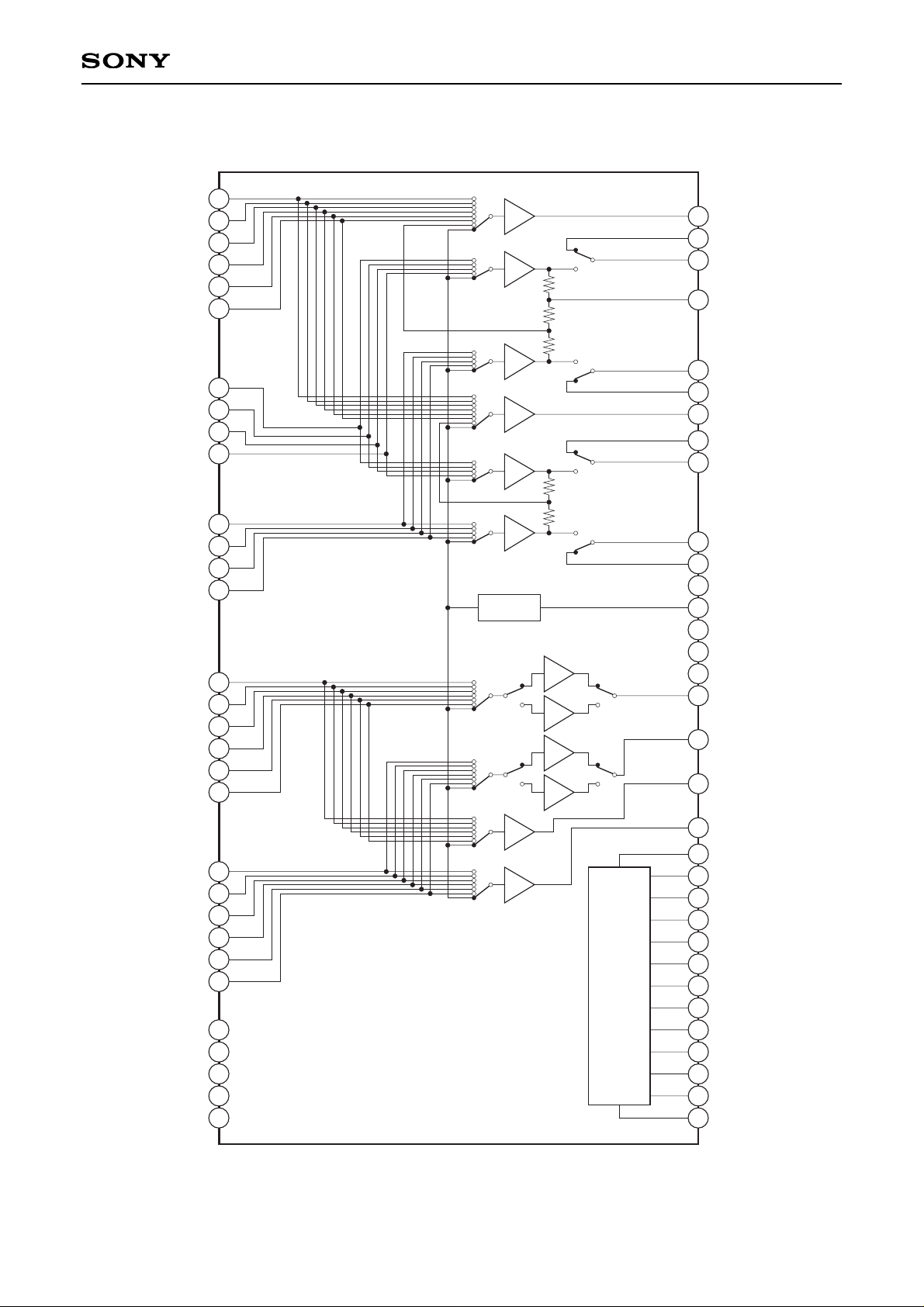
Block Diagram
29
30
31
46
47
VOUT1
YOUT1
LV5
V5
RV5
LTV
TV
RTV
NC
NC
NC
C4
RV4
Y4
LV4
V4
V3
V2
V1
Y3
Y2
Y1
C3
C2
C1
LV3
LV2
LV1
RV3
RV2
RV1
NC
NC
YIN1
LOUT1
ROUT1
TRAP1
VGND
COUT1
CIN1
VOUT2
YIN2
YOUT2
COUT2
CIN2
AGND2
BIAS
V
CC
AGND
LOUT2
ROUT2
6dB
6dB
6dB
6dB
6dB
6dB
BIAS
6dB
0dB
6dB
0dB
6dB
6dB
49
53
56
40
39
38
37
35
41
42
43
44
45
ADR
S-4
S2-4
S-3
S2-3
SDA
SCL
DC OUT
S-2
S-1
S2-2
S2-1
MUTE
Logic
6
7
13
14
20
21
27
28
36
34
32
33
48
50
51
52
54
55
57
58
4
11
18
25
64
61
8
15
22
60
63
1
3
5
10
12
17
19
24
26
2
9
16
23
59
62
Audio system is attenuated by 6dB for 6kΩ resistor input, and a total gain is 0dB (LOUT1 and ROUT1 can be changed to –6dB).
– 3 –
CXA2079Q
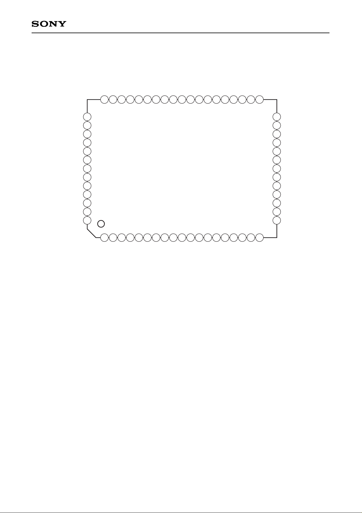
Pin Configuration
2
3
4
5
6
7
8
9
10
11
12
13
14
15
16
17
18
19
20
21
22
23
24
25
26
27
28
29
30
40
39
38
37
36
35
34
31
32
33
41
42
43
44
45
46
47
48
49
50
51
52
53
54
55
56
57
58
59
60
63
64
61
62
1
LOUT1
VOUT1
ROUT1
TRAP1
YOUT1
VGND
COUT1
LV5
V5
RV5
LTV
TV
RTV
ADR
NC
NC
NC
S-4
S2-4
C4
RV4
Y4
LV4
V4
S-3
S2-3
CIN1
BIAS
YIN1
MUTE
NC
NC
YIN2
AGND2
CIN2
V
CC
VOUT2
ROUT2
YOUT2
LOUT2
COUT2
DC OUT
AGND
SDA
SCL
V1
LV1
Y1
RV1
C1
S2-1
S-1
V2
LV2
Y2
RV2
C2
S2-2
S-2
V3
LV3
Y3
RV3
C3
– 4 –
CXA2079Q
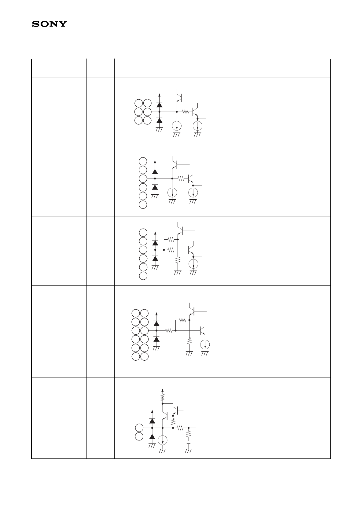
Pin Description
Pin
No.
63
1
8
15
22
60
TV
V1
V2
V3
V4
V5
4.0V
Video signal inputs.
Input composite video signals.
Symbol
Pin
voltage
Equivalent circuit Description
150
VCC
3µA
8
15
22
60
63
1
3
10
17
24
49
45
Y1
Y2
Y3
Y4
YIN1
YIN2
4.0V
Y/C separation signal inputs.
Input luminance signals.
The YIN1 pin inputs the signal
obtained by Y/C separating the
VOUT1 pin output.
The YIN2 pin inputs the signal
obtained by Y/C separating the
VOUT2 pin output.
3
10
17
24
45
49
150
VCC
3µA
5
12
19
26
51
43
C1
C2
C3
C4
CIN1
CIN2
4.5V
Y/C separation signal inputs.
Input chrominance signals.
The CIN1 pin inputs the signal
obtained by Y/C separating the
VOUT1 pin output.
The CIN2 pin inputs the signal
obtained by Y/C separating the
VOUT2 pin output.
150
V
CC
27k
20k
5
12
19
26
43
51
62
2
9
16
23
59
64
4
11
18
25
61
LTV
LV1
LV2
LV3
LV4
LV5
RTV
RV1
RV2
RV3
RV4
RV5
4.5V Audio signal inputs.
VCC
15k
33k
27k
2
4
9
11
16
18
23
25
59
64
61
62
5341VOUT1
VOUT2
3.9V
Video signal outputs.
Output composite video signals.
VCC
27k
VCC
23.5k
30k
250
41
53
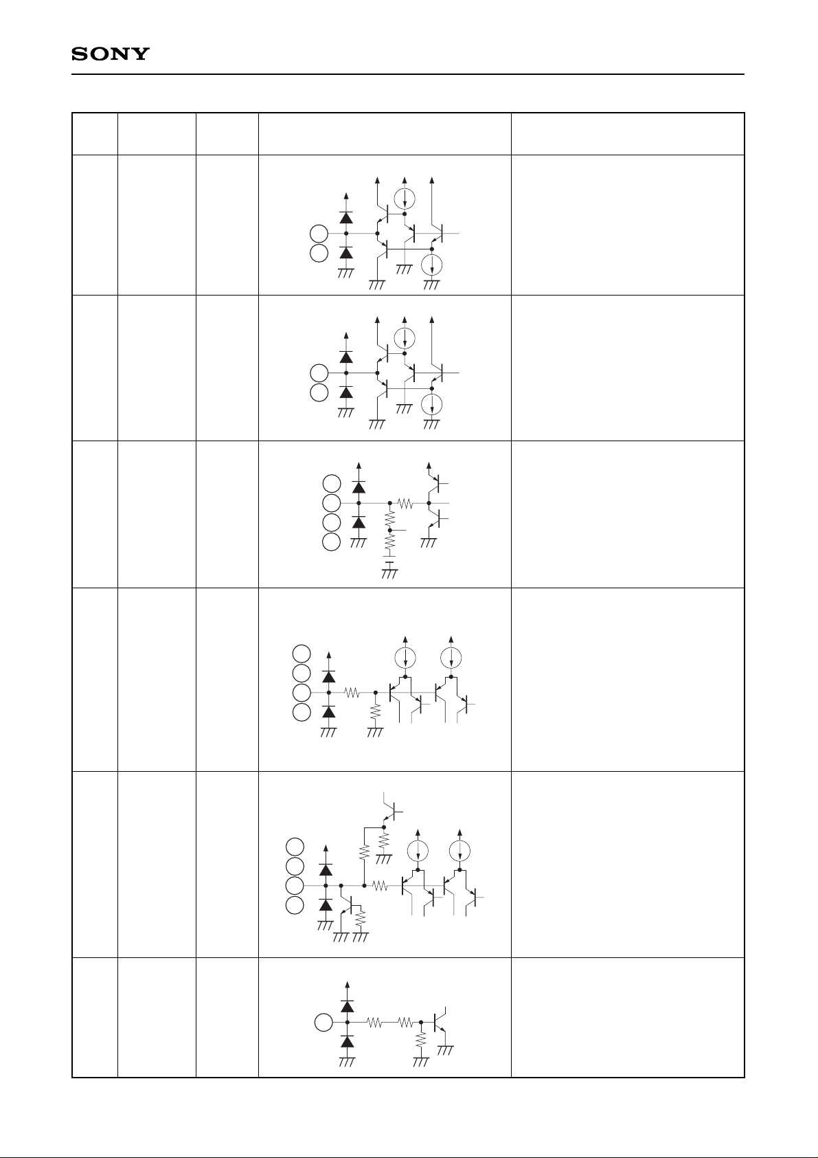
– 5 –
CXA2079Q
5837COUT1
COUT2
4.5V
Video signal outputs.
Output chrominance signals.
VCC
VCC VCC VCC
37
58
56
39
YOUT1
YOUT2
3.3V
Video signal outputs.
Output luminance signals.
VCC
VCC VCC VCC
39
56
52
38
54
40
LOUT1
LOUT2
ROUT1
ROUT2
4.5V
Audio signal outputs.
Zo = 50Ω (within DC ± 2mA)
VCC
VCCVCC
147
100k
6
13
20
27
6
13
20
27
S2-1
S2-2
S2-3
S2-4
—
Detects the S2-compatible DC
superimposed onto the C signal.
4:3 video signal at 1.3V or less
4:3 letter-box signal at 1.3V or more
to 2.5V or less
16:9 picture squeezed signal at 2.5V
or more
These pins are pulled down to GND
by a 100kΩ resistor, so the 4:3 video
signals are selected when open.
VCC VCC
20k
56
20k
40
38
52
54
7
14
21
28
S-1
S-2
S-3
S-4
—
Composite video/S selector.
The detection results are written to
the status register.
S signal at 3.5V or less
Composite video signal at 3.5V or
more
These pins are pulled up to 5V by a
100kΩ resistor, so the composite
video signals are selected when
open.
VCC
VCCVCC
50k
10k
100k
50k
5V
7
14
21
28
32
ADR —
Selects the slave address for the I2C
bus.
90H at 1.5V or less
92H at 2.5V or more
90H when open
VCC
147
28k
72k
32
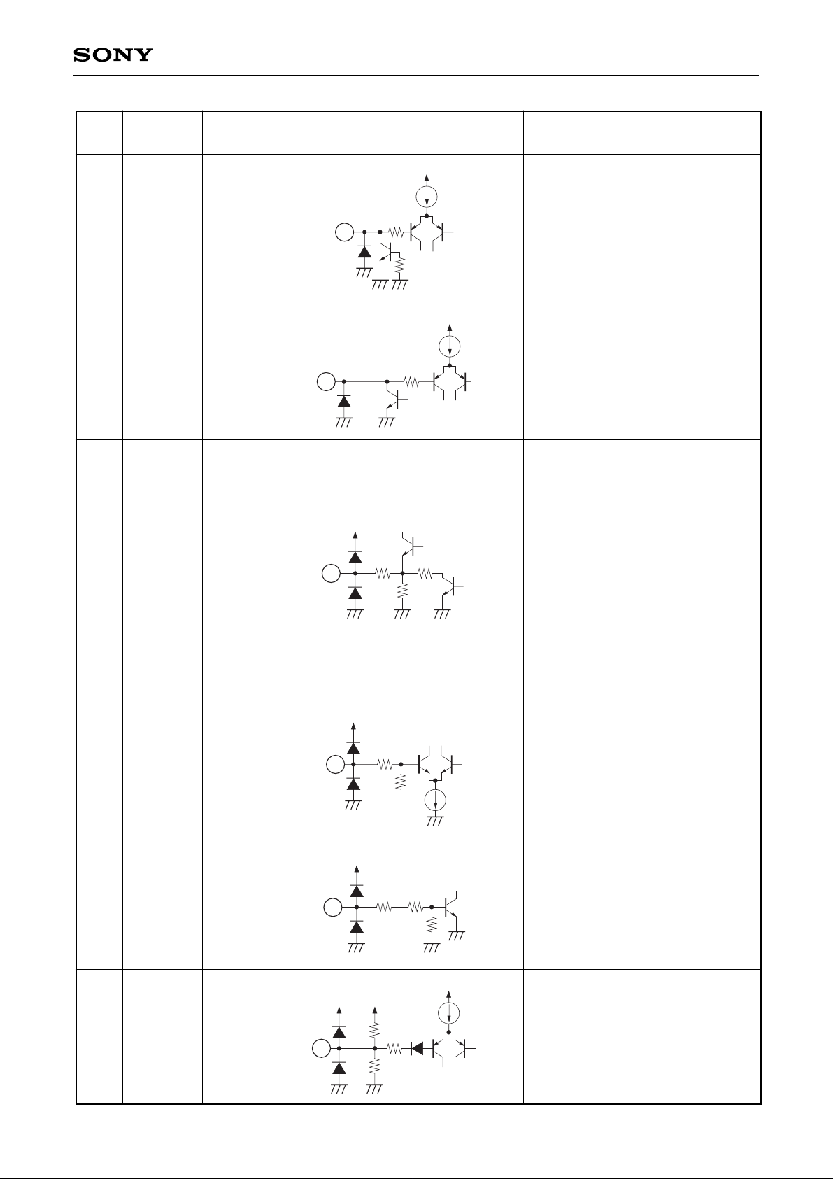
Pin
No.
Symbol
Pin
voltage
Equivalent circuit Description
– 6 –
CXA2079Q
34 SDA
—
I2C bus signal input
VILmax = 1.5V
VIHmin = 3.0V
VOLmax = 0.4V
VCC
4k
34
33
SCL
—
I2C bus signal input
VILmax = 1.5V
VIHmin = 3.0V
33
VCC
4k
10k
36
DC OUT —
Outputs the S2-compatible DC
superimposed onto the COUT2
output. The DC is superimposed by
connecting this pin to the COUT2
output via a capacitor.
Control is performed by the I2C bus.
When 0V is output, Q1 is ON and
the impedance is 5kΩ.
S2 protocol output DC impedance of
10 ± 3kΩ is realized by attaching
external resistance of 4.7kΩ.
DC OUT (bus) Output DC
0 4.5V
1 0V
2 1.9V
3 4.5V
VCC
100
1k
55
55
TRAP1 3.8V
Connects trap circuit for subcarrier.
36
VCC
4k
28k
1k
Q1
48 MUTE —
Audio signal output mute.
Mute OFF at 1.5V or less
Mute ON at 2.5V or more
Mute OFF when open
VCC
147
28k
72k
48
50
BIAS 4.5V
Internal reference bias (Vcc/2).
Connects to GND via a capacitor.
VCC
VCC
147
20k
VCC
20k
50
Pin
No.
Symbol
Pin
voltage
Equivalent circuit Description
 Loading...