

Sony CXA2076Q Datasheet

Description
The CXA2076Q is a bipolar IC which integrates the
luminance signal processing, chroma signal
processing, RGB signal processing, and sync and
deflection signal processing functions for NTSC/PAL
system color TVs onto a single chip. This IC includes
deflection processing functions for wide-screen TVs,
and is also equipped with a SECAM decoder
interface, making it possible to construct a TV
system that supports multiple color systems.
Features
• I2C bus compatible
• Compatible with both PAL and NTSC systems
(also compatible with SECAM if a SECAM decoder is connected)
• Built-in deflection compensation circuit capable of supporting various wide modes
• Countdown system eliminates need for H and V oscillator frequency adjustment
• Automatic identification of 50/60Hz vertical frequency (forced control possible)
• Non-interlace display support (even/odd selectable)
• Automatic identification of PAL, NTSC, and SECAM color systems (forced control possible)
• Automatic identification of 4.43MHz/3.58MHz crystal (forced control possible)
• Non-adjusting Y/C block filter
• One CV input, one set of Y/C inputs, two sets of analog RGB inputs (one set of which can serve as both
analog and digital inputs)
• Built-in AKB circuit
• Support for forcing YS1 off
Applications
Color TVs (4:3, 16:9)
Structure
Bipolar silicon monolithic IC
Absolute Maximum Ratings (Ta = 25°C, SGND, DGND = 0V)
• Supply voltage SVCC1, 2, DVCC1, 2 –0.3 to 12 V
• Operating temperature Topr –20 to +65 °C
• Storage temperature Tstg –65 to +150 °C
• Allowable power dissipation PD 1.7 W
(when mounted on 50mm × 50mm board)
• Voltages at each pin –0.3 to SVCC1, SVCC2,
DVCC1, DVCC2 + 0.3 V
Operating Conditions
Supply voltage SVCC1, 2 9.0 ± 0.5 V
DVCC1, 2 9.0 ±0.5 V
– 1 –
CXA2076Q
E96Z27-PS
Y/C/RGB/D for PAL/NTSC Color TVs
Sony reserves the right to change products and specifications without prior notice. This information does not convey any license by
any implication or otherwise under any patents or other right. Application circuits shown, if any, are typical examples illustrating the
operation of the devices. Sony cannot assume responsibility for any problems arising out of the use of these circuits.
64 pin QFP (Plastic)
– 2 –
CXA2076Q
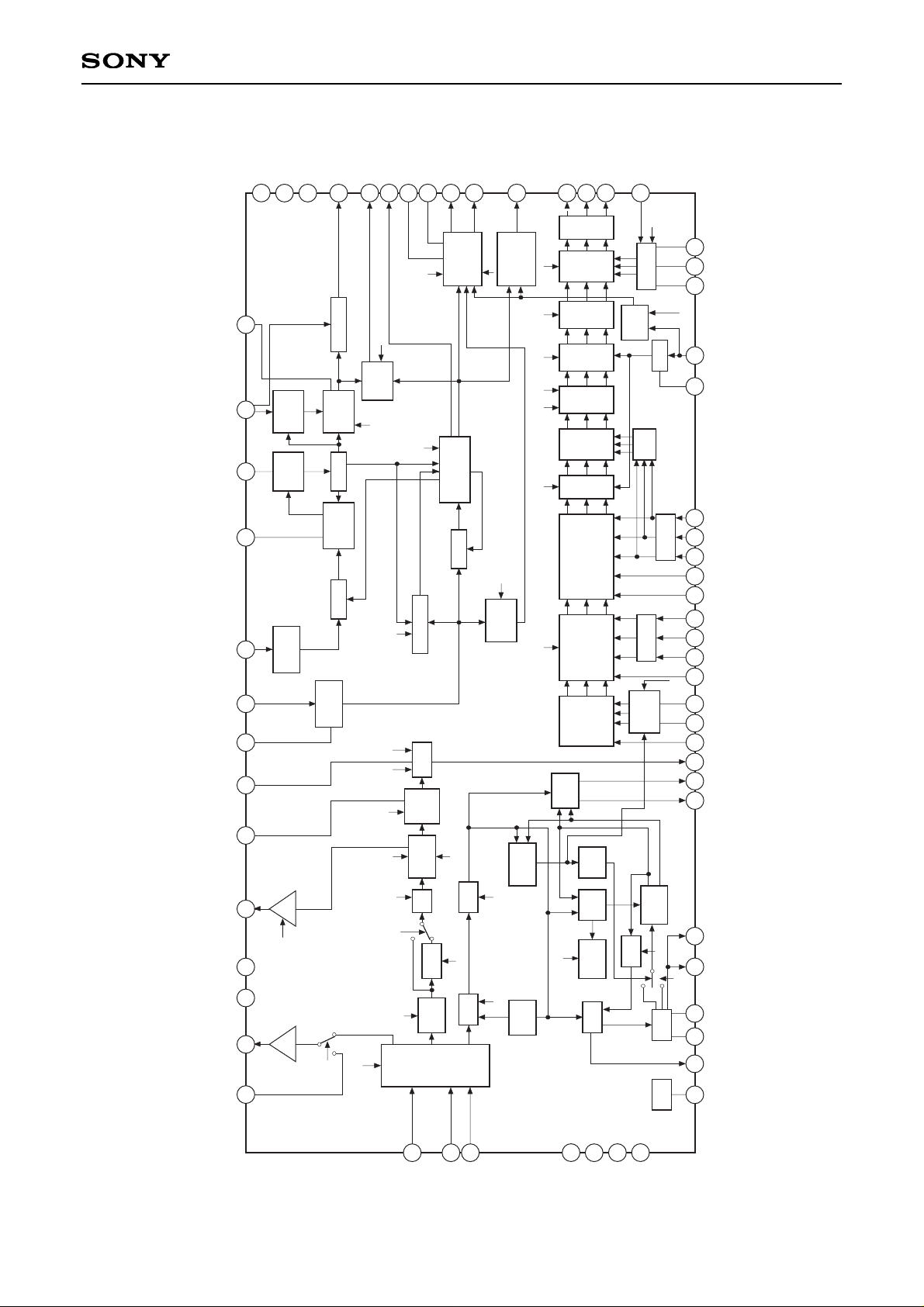
Block Diagram
VIDEO
SW
SHARP
NESS
SUB
CONT
TRAP
KILLER
DET
ACC
DET
DL
DC
TRAN
CLP
D PIC
WIDE
Sawtooth
Gen.
AKB
BLK
CV/YC
TRAP OFF
DL
SHARP
DC
TRAN
D PICAGING
VM OFF
SUB COLOR
TRAP F0
TOT
ACC
PRE/OVER
TOT
PAL
ID
PAL/
NTSC
DEM
APC
HUE
VCO
DEM
AXIS
IREF
fsc
ID
COLOR SW
fsc R-Y
fsc B-Y
V SYNC
SEP
H SYNC
SEP
1Vp-p
CVIN
YIN
CIN
SV
CC1SVCC2
SGND1
SGND2
XTAL
HUE
IREF
APCFIL
X358
X443
FSCOUT
SECAMREF
–(R-Y) OUT
–(B-Y) OUT
YOUT
YRET
–(R-Y) IN
–(B-Y) IN
YS1
R1IN
G1IN
B1IN
YS2
YM
R2IN
G2IN
B2IN
ABLFIL
CUT
OFF
GB
DRV
BRT
D-
COL
γ
OSD
MIX
PIC
YS/YM
SW
Y/C
MIX
COLOR
& AXIS
COL
CLP
CLP
DIG
HV
COMP
ABL
EHT H, V
AKB OFF
IKIN
BOUT
GOUT
ROUT
E-WOUT
VD–OUT
/VPROT
VD+OUT
/VPROT
SAWOSC
VAGCSH
VTIM
SCPOUT
HD OUT
DGND
DV
CC2DVCC1
ABLIN/
VCOMP
RSH
GSH
BSH
L2FIL
AFCPIN/
HOFF
CERA
AFCFIL
HSIN
VSIN
VSFIL
BLHOLD
DCTRAN
VM
SCL
SDA
SYNCOUT
EXT SYNC IN
GB CUT
GB DRV
BRT
γ
PIC
WIDE
Parabola
Gen.
VLIN, SCORR
VPOSI, VOFF,
VSIZE
Count Down
525/625
INTER
-LACE
D-COL
GATE
50/60 ID
GATE
PHASE
DET.
1/32
PHASE
SHIFT
PHASE
DET
32fH
VCO
2fH
H POSI
AFC
C MODE
INTERLACE
V FREQ
SCP BGR/BGF
40
39
38
41
45
46
47
48
49
50
51
52
54
56
2
9
20
59
53
55
57
43
60
64
61
62 1
3
4
5
6
7
8
11
12
13
14
15
16
17
18
19
21
23
25
28
29
10
22
24
26
30
37
36
35
34
31
32
33
42
44
27
2Vp-p
1Vp-p
EXT
SYNC
6dB
H.DRIVE
YS1 OFF
YS
SW
SUB CONT
Sand
Castle
– 3 –
CXA2076Q
Pin Configuration
HSIN
E-WOUT
VSFIL
L2FIL
IREF
SAWOSC
CERA
HDOUT
SDA
VAGCSH
VSIN
AFCFIL
DV
CC
2
DV
CC
1
DGND
AFCPIN/HOFF
VM
SCL
SYNCOUT
EXT SYNC IN
TEST
APCFIL
X358
BLHOLD
CIN
NC
SV
CC1
X443
DCTRAN
CVIN
YIN
ABLIN/VCOMP
BOUT
SV
CC2
GOUT
ROUT
IKIN
RSH
BSH
GSH
VTIM
VD–OUT/VPROT
ABLFIL
40
39
38
37
36
4142
43
44
45
46
47
48
49
50
51
35
34
33
26
27
28
29
30
31
32
20
21
22
23
24
25
YOUT
B2IN
–(R-Y) IN
G1IN
SGND2
R2IN
YS1
YS2
SECAMREF
G2IN
YRET
R1IN
–(B-Y) IN
YM
SCPOUT
B1IN
–(R-Y) OUT
SGND1
–(B-Y) OUT
2
3
4
5
6
7
8
9
10
11
12
13
14 15
16
17
18
19
1
52
53
54
55
56
57
58
59
60
63
64
61
62
FSCOUT
VD+OUT/VPROT
– 4 –
CXA2076Q
SECAM decoder interface. This pin
serves as both a 4.43MHz output and as
a SECAM identification input/output pin.
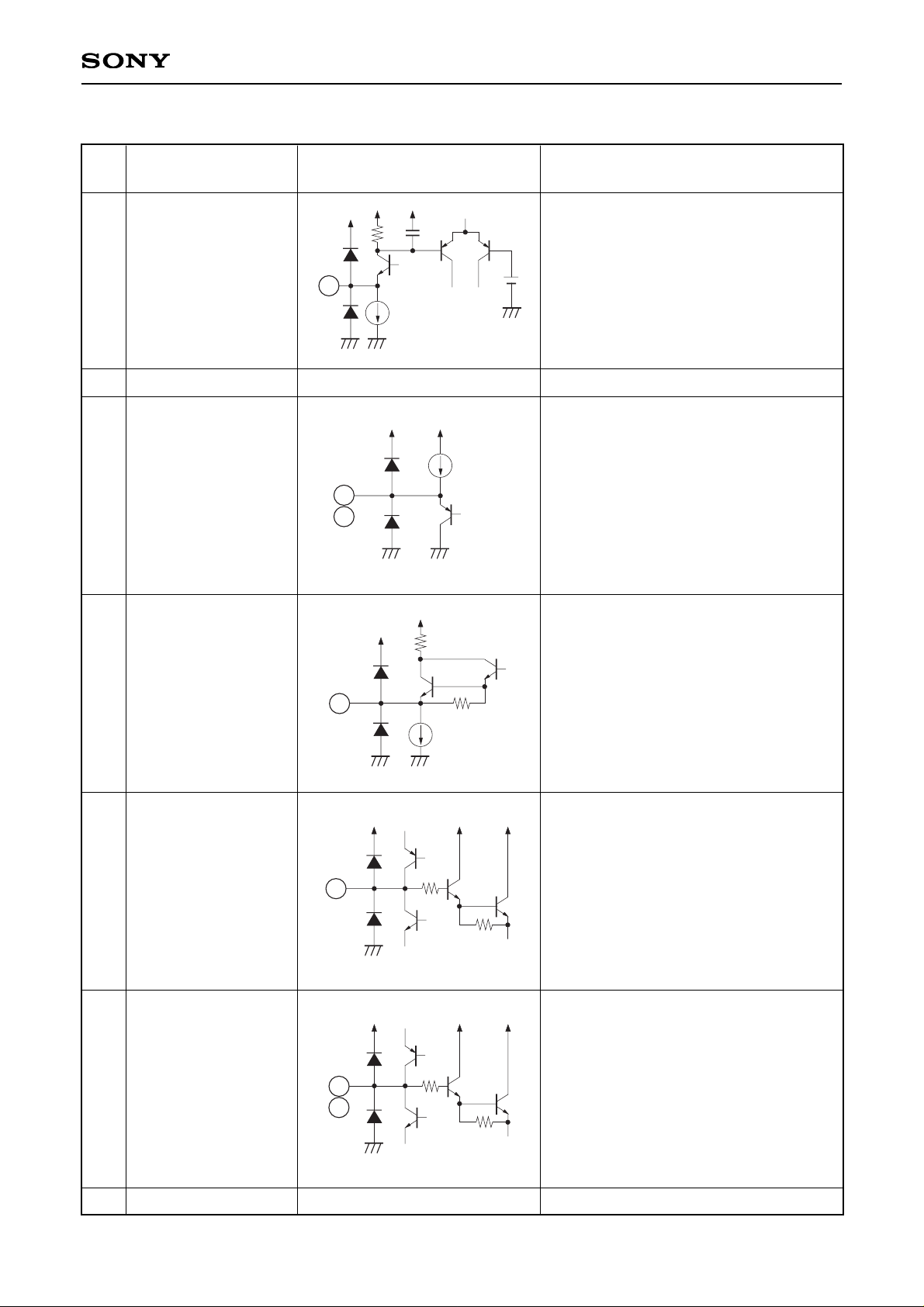
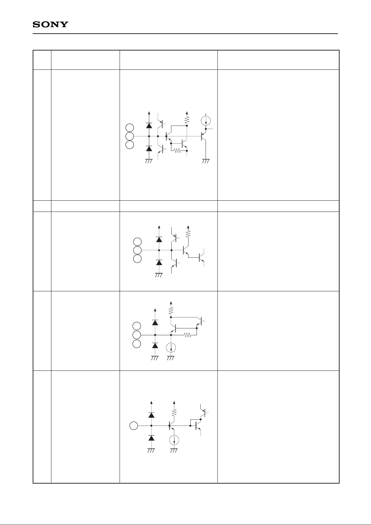
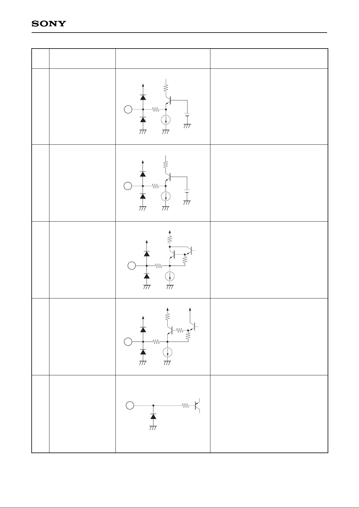
Pin Description
Pin
No.
Symbol Equivalent circuit Description
1
SECAMREF
3
4
–(R-Y) OUT
–(B-Y) OUT
Color difference signal outputs. Go to
high impedance when the SECAM
system is detected.
Standard output levels for 75% CB:
B-Y: 0.665Vp-p
R-Y: 0.525Vp-p
5
YOUT
Luminance signal output.
Black level is 3.5VDC.
Standard output level for 100 IRE input:
1Vp-p
6
YRET
Luminance signal input.
Clamped to 4.8V at the burst timing.
Standard input level for 100 IRE input:
1Vp-p
7
8
–(R-Y) IN
–(B-Y) IN
Color difference signal inputs.
Clamped to 5.5V at the burst timing.
Standard input levels for 75% CB:
B-Y: 1.33Vp-p
R-Y: 1.05Vp-p
2
SGND1 GND for Y/C block.
9
SGND2 GND for the RGB block.
1
250µA
6k
20p
7.2V
3
200µA
4
700µA
500
30k
5
6
1.5k
70k
7
8
1.5k
70k
—
– 5 –
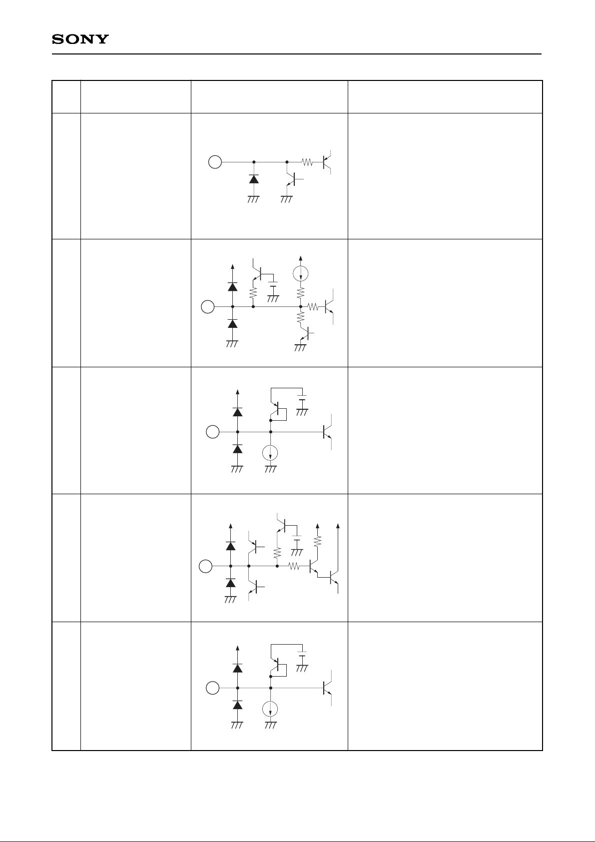
CXA2076Q
YSSW control input.
When YS is high, the RGB1 block signal
is selected; when YS is low, the Y/C block
is selected. This function can be disabled
by the YS1OFF setting for the I2C bus.
VILMAX = 0.4V
VIHMIN = 1.0V
10
SCPOUT
Sand castle pulse output. The 0 to 5V
BGP pulse, the phase of which is
controlled through the bus, is
superimposed with the 0 to 2V H and
VBLK pulse for output.
11
YS1
12
13
14
R1IN
G1IN
B1IN
Analog R, G and B signal inputs.
Input a 0.7Vp-p (no sync, 100 IRE) signal
via a capacitor.
The signal is clamped to 5.7V at the burst
timing of the signal input to the HSIN
input pin (Pin 47).
15
YS2
YS/YMSW YS control input.
When YS is high, the RGB2 block signal
is selected; when YS is low, the YSSW
output signal is selected.
VILMAX = 0.4V
VIHMIN = 1.0V
10k
1k
1k
10
100µA
40k
11
12
13
14
30k
200
100µA
40k
15
16
YM
YS/YMSW YM control input.
When YM is high, the YSSW output
signal is attenuated by 9.6dB.
VILMAX = 0.4V
VIHMIN = 1.0V
100µA
40k
16
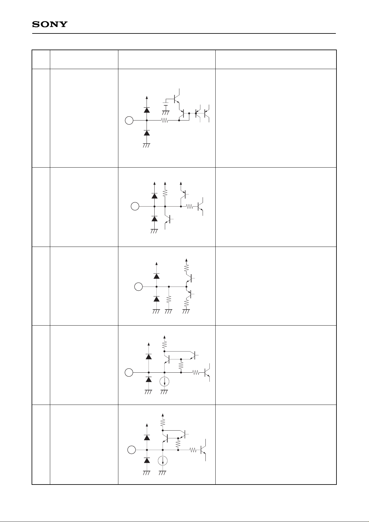
Pin
No.
Symbol Equivalent circuit Description
– 6 –
CXA2076Q
Power supply for RGB block.
17
18
19
R2IN
G2IN
B2IN
Analog/digital (dual-purpose) RGB signal
inputs.
The input signals are input via capacitors.
When using analog input, input a 0.7Vp-p
signal (no sync, 100 IRE); when using
digital input, input a signal of at least
1.5Vp-p (Vth = 1.2V).
The display level is 67 IRE. When using
digital input, digital input is selected
regardless of the YS setting.
In addition, the VM output is turned off.
These pins are clamped to 5.7V at the
burst timing of the signal input to the
sync input pin (Pin 47).
30k
200
19
17
18
100µA
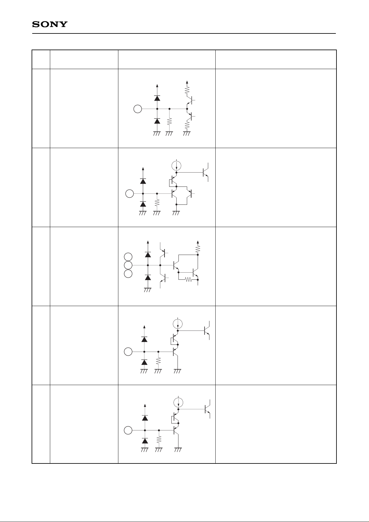
21
23
25
RSH
GSH
BSH
Sample-and-hold for R, G and B AKB.
Connect to GND via a capacitor.
When not using AKB (manual CUTOFF
mode), R, G and B cut-off voltage can be
controlled by applying a control voltage to
each pin. The control voltage is 4.5 ± 1V.
200
21
23
25
22
24
26
ROUT
GOUT
BOUT
R, G and B signal outputs.
2.5Vp-p is output during 100% white
input.
1.1mA
200
12k
22
24
26
27
IKIN
Input the signal converted from the CRT
beam current (cathode current Ik) to a
voltage via a capacitor. The V blanking
part is clamped to 2.7V at the V retrace
timing.
The input for this pin is the reference
pulse return, and the loop operates so
that the Rch is 1Vp-p and the G and Bch
are 0.81Vp-p. The G and Bch can be
varied by ±0.5V by the bus CUTOFF
control. When not using AKB, this pin
should be open.
1k
27
50µA
20
SVCC2
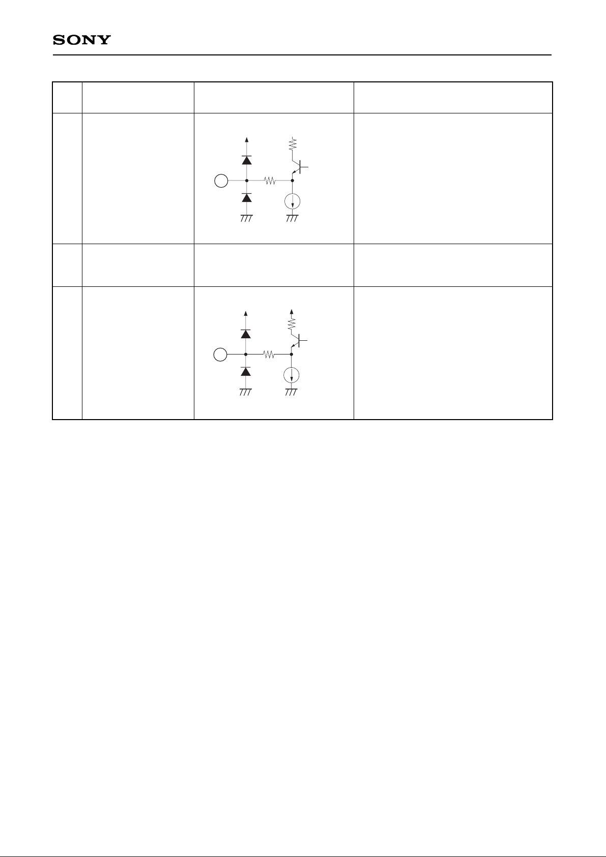
Pin
No.
Symbol Equivalent circuit Description
– 7 –
CXA2076Q
Connect a capacitor to form the LPF of
the ABL control signal.
28
ABLIN/VCOMP
ABL control signal input and VSAW high
voltage fluctuation compensation signal
input.
High voltage compensation has linear
control characteristics for the pin voltage
range of about 8V to 1V. The control
characteristics can be varied through
EHT-V control of the bus. ABL begins to
have effect below a threshold voltage of
about 1.2V.
ABL functions as PIC/BRT-ABL (average
value type).
29
ABLFIL
30
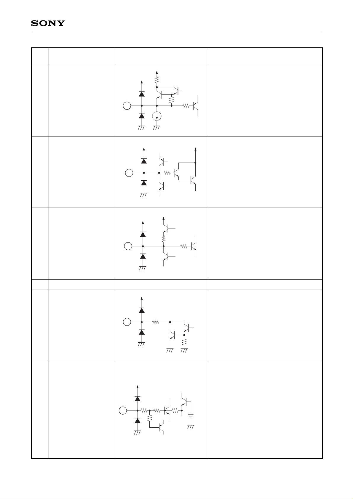
VTIM
V timing pulse output.
Outputs the timing pulse from V sync
identification to the end of V blanking.
Pulses are positive polarity from 1 to 6V.
During zoom mode, the V blanking pulse
which has been expanded before and
after the V sync is superimposed and
output as the 1 to 3V pulse.
1.5V
147
28
29
1.2k
100k
10k
1k
1k
30
31
VD–OUT/VPROT
V sawtooth wave output and V protect
signal input.
When a large current (3mA) is drawn
from this pin, the RGB outputs are all
blanked and "1" is output to the status
register VNG.
31
400µA
700
24k
30k
32
VD+OUT/VPROT
Serves as both a V sawtooth wave output
with the reverse polarity of VD–OUT,
and a Vprotect signal input. The Vprotect
function can even be applied to this pin.
400µA
700
30k
24k
32
Pin
No.
Symbol Equivalent circuit Description
– 8 –
CXA2076Q
H deflection pulse input for H AFC.
Input an about 5Vp-p pulse via a
capacitor. Set the pulse width to 10 to
12µs. This pin is also used as the holddown signal input for the HD output, and
if this pin is 1V or less for a 7V cycle or
longer, the hold-down function operates
and the HD output is held to 9VDC. In
addition, the RGB outputs are all blanked.
Outputs "1" to the status register XRAY.
38
33
E-WOUT
V parabola wave output.
34
VAGCSH
Sample-and-hold for AGC which
maintains the V sawtooth wave at a
constant amplitude.
Connect to GND via a capacitor.
800µA
15k
78k
1.4k
33
1.2k
34
35
SAWOSC
Connect a capacitor to generate the V
sawtooth wave. For the capacitor, use an
MPS (metalized polyester capacitor), etc.,
with a small tan δ.
100
300
35
36
DVCC1 Power supply for the V deflection block.
37
HD OUT
H drive signal output.
This signal is output with the open
collector.
147
37
20k
AFCPIN/HOFF
10k
68k
38
10k
147
4.2V
Pin
No.
Symbol Equivalent circuit Description
– 9 –
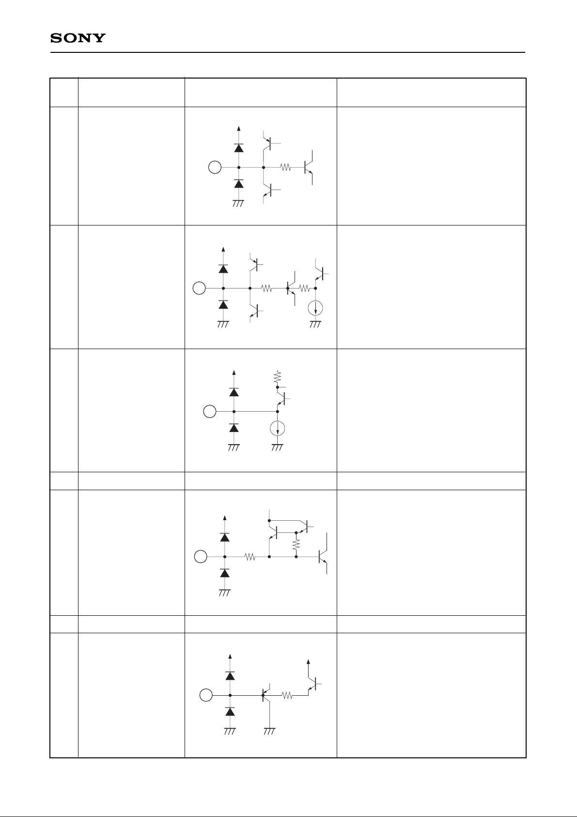
CXA2076Q
CR connection for the AFC lag-lead filter.
IREF
39
L2FIL
Filter for H AFC.
Connect to GND via a capacitor.
The H phase can also be controlled from
this pin by leading current in and out of
this capacitor.
As the pin voltage rises, the picture shifts
to the left; as the pin voltage drops, the
picture shifts to the right.
40
AFCFIL
100
39
46k
1.2k
40
41
CERA
Connect the 32 × FH VCO ceramic
oscillator.
41
400µA
10k
42
44
DGND
DVCC2 Power supply for the H deflection block.
GND for the deflection block.
43
Internal reference current setting.
Connect to GND via a resistor with an
error of less than 1% (such as a metal
film resistor).
147
43
20k
45
VSFIL
Filter for V sync separation.
Connect to GND via a capacitor.
1k
45
Pin
No.
Symbol Equivalent circuit Description
– 10 –
CXA2076Q
Sync signal output for VSIN and HSIN.
The output can be selected from the
internal sync signals (Pin 53 or Pin 55) or
the external sync signal (Pin 56) by the
I2C bus.
Output signal level: 2Vp-p
(0.6Vp-p sync only)
Input/output gain: 6dB
46
VSIN
Sync signal input for V sync separation.
Input a 2Vp-p Y signal (or a 0.6Vp-p
sync signal).
47
HSIN
Sync signal input for H sync separation.
Input a 2Vp-p Y signal (or a 0.6Vp-p sync
signal).
48
SYNCOUT
147
4.1V
46
20µA
15k
147
3.2V
10µA
14k
47
240µA
1.2k
40k
48
147
49
VM
Outputs the differential waveform of the
VM (Velocity Modulation) Y signal.
(6.6VDC, 1.1Vp-p)
The signal advanced for 200ns from
YOUT is output. The delay time versus
YIN is determined by the DL setting of
the I2C bus. This output can be turned off
through the I2C bus.
This output can also be turned off by
YS1, YM, and YS2.
400µA
500
30k
147
49
1.2k
50
SCL
I2C bus protocol SCL (Serial Clock) input.
VILMAX = 1.5V
VIHMIN = 3.5V
4k
50
Pin
No.
Symbol Equivalent circuit Description
– 11 –
CXA2076Q
Capacitor connection for black peak hold
of the dynamic picture (black expansion).
51
SDA
I2C bus protocol SDA (Serial Data) I/O.
VILMAX = 1.5V
VIHMIN = 3.5V
VOLMAX = 0.4V
52
BLHOLD
53
CVIN
Composite video signal input.
Input the 1Vp-p (100% white including
sync) CV signal via a capacitor. The
sync level of the input signal is
clamped to 3.8V.
4k
51
1.2k
4k
52
9µA
20k
20k
4.6V
1µA
4.6V
53
54
DCTRAN
Connect a capacitor that determines the
DC transmission ratio to GND.
2k
54
2V
1.2k
4k
55
YIN
Y signal input.
Input a 1Vp-p (100% white including
sync) Y signal via a capacitor. The
sync level of the input signal is
clamped to 3.8V.
1µA
4.6V
55
Pin
No.
Symbol Equivalent circuit Description
– 12 –
CXA2076Q
Chroma signal input.
Input a C signal with a burst level of
300mVp-p via a capacitor. Input signal is
biased to 4.5V internally.
56
EXT SYNC IN
External sync signal input.
Input a 0.3Vp-p sync signal (or a 1Vp-p
CV signal or Y signal) via a capacitor.
The sync level of the input signal is
clamped to 3.8V.
57
CIN
1µA
4.6V
56
30k
5.2V
50k
57
58
TEST
Test pin.
Outputs a 0 to 3V V-SYNC SEP with
positive polarity. If not used, leave this
pin open.
15k
1k
58
59
SVCC1 Power supply for Y/C block.
60
APCFIL
CR connection for the chroma APC laglead filter.
1.2k
4.6V
1.2k
60
61
X443
Connect a 4.433619MHz crystal oscillator.
200µA
4k
61
500
Pin
No.
Symbol Equivalent circuit Description
– 13 –
CXA2076Q
Not connected.
Normally connected to GND to prevent
interference with other pins.
62
X358 Connect a 3.579545MHz crystal oscillator.
200µA
4k
500
62
64
FSCOUT
Subcarrier output.
Output level: 5.2VDC, 0.4Vp-p
280µA
1.2k
147
64
63
NC
Pin
No.
Symbol Equivalent circuit Description
– 14 –
CXA2076Q
Electrical Characteristics
Setting conditions • Ta = 25°C, SVCC1, 2 = DVCC1, 2 = 9V, SGND1, 2 = DGND = 0V
• Measures the following after setting the I
2
C bus register as shown in "I
2
C Bus Register Initial Settings".
1
2
3
4
5
6
7
8
9
SICC
DICC
fHFR
∆fHR
HDw
VBLKh
VBGPh
VSp-p
VSdc
90
67
15.90
400
26.5
12.6
3.3
1.1
3.1
42
30
15.55
–400
24.5
11.6
2.5
0.9
2.9
Measure the pin inflow current.
Measure the pin inflow current.
HDRIVE output frequency
Confirm that I
2
C status register
HLOCK is 1 (the pull-in range
when f
H is shifted from
15.734kHz).
Measure the pulse width for the section
where the HDRIVE output is high.
Measure the VDRIVE output Vp-p.
V
CC = 9.0V,
Bus data = center
V
CC = 9.0V,
Bus data = center
AFC MODE = 0h
SYNCIN: composite sync
SYNCIN: composite sync
SCP
Measure the pulse width for the
section where the BLK output is high.
SCP
Measure the pulse width for the section
where the BGP output is high.
SYNCIN: composite sync
Signal block current
consumption
Sync block current
consumption
Horizontal free-running
frequency
Horizontal sync pull-in
range
HD output pulse width
SCP
BLK output pulse width
SCP
BGP output pulse width
VDRIVE output
amplitude
VDRIVE output center
potential
20, 59
36, 44
37
—
37
10
10
31, 32
31, 32
mA
mA
kHz
Hz
µs
µs
µs
V
V
No. Item Symbol Measurement conditions
Measurement pins
Measurement contents Min. Typ. Max. Unit
Sync deflection block items
VBGPh
VBLKh
VSp-p
10.79ms
VDRIVE+
VSdc
46: VSIN in
65
48
15.734
—
25.5
12.1
2.9
1.0
3.0
– 15 –
CXA2076Q
Measure the EWDRIVE output
Vp-p.
Output amplitude when a video
signal with an amplitude of
0.7Vp-p/100 IRE is input.
Input fsc to CVIN.
Ratio of the fsc component of the
Yout amplitude when CTRAP = 1
against the Yout amplitude when
CTRAP = 0.
SYNCIN: composite sync
TRAPOFF = 0/1
TRAP-F0 = 7h
10
11
12
13
14
EWDRIVE output
amplitude
EWDRIVE output
center potential
R, G and B output
amplitude
R, G and B output
linearity
C-TRAP attenuation
(3.58MHz)
VEWp-p
VEWdc
VRout1
Lin
C-Trap3.58
33
33
22, 24, 26
22, 24, 26
22
0.42
3.8
2.25
96
—
0.52
3.95
2.5
100
–30
0.62
4.1
2.85
104
—
V
V
V
%
dB
No. Item Symbol Measurement conditions
Measurement pins
Measurement contents Min. Typ. Max. Unit
Signal block items
VEWp-p
10.79ms
VEW dc
46: VSIN in
V1
V2
Lin =
V2 × 2
V1
× 100
f = 3.58MHz
CVIN:
0.7Vp-p
/100 IRE
CVIN:
100 IRE
50 IRE
CVIN:
fsc, 50 IRE
 Loading...