

Sony CXA2074S, CXA2074Q Datasheet

– 1 –
CXA2074Q/S
E96843B86
US Audio Multiplexing Decoder
Description
The CXA2074Q/S is an IC designed as a decoder
for the Zenith TV Multi-channel System and also
corresponds with I2C BUS. Functions include stereo
demodulation, SAP (Separate Audio Program)
demodulation, dbx noise reduction and sound
processor. Various kinds of filters are built in while
adjustment, mode control and sound processor
control are all executed through I2C BUS.
Features
• Audio multiplexing decoder, dbx noise reduction
decoder and sound processor are all included in a
single chip. Almost any sort of signal processing is
possible through this IC.
• All adjustments are possible through I2C BUS to
allow for automatic adjustment.
• Various built-in filter circuits greatly reduce external
parts.
• There are three systems for inputs and two
systems for outputs, and each mode control is
possible.
Standard I/O Level
[( ) is the pin No. for the CXA2074S.]
• Input level
COMPIN (Pin 17) 245mVrms
AUX1-L/R (Pins 36 and 35) 490mVrms
AUX2-L/R (Pins 38 and 37) 490mVrms
• Output level
LPOUT-L/R (Pins 40 and 39) 490mVrms
LSOUT-L/R (Pins 8 and 7) 490mVrms
Absolute Maximum Ratings (Ta = 25°C)
• Supply voltage VCC 11 V
• Operating temperature Topr –20 to +75 °C
• Storage temperature Tstg –65 to +150 °C
• Allowable power dissipation
PD 0.6 (48 pin QFP) W
2.2 (42 pin SDIP) W
Range of Operating Supply Voltage
9 ± 0.5 V
Applications
TV, VCR and other decoding systems for US audio
multiplexing TV broadcasting
Structure
Bipolar silicon monolithic IC
∗ A license of the dbx-TV noise reduction system is
required for the use of this device.
Sony reserves the right to change products and specifications without prior notice. This information does not convey any license by
any implication or otherwise under any patents or other right. Application circuits shown, if any, are typical examples illustrating the
operation of the devices. Sony cannot assume responsibility for any problems arising out of the use of these circuits.
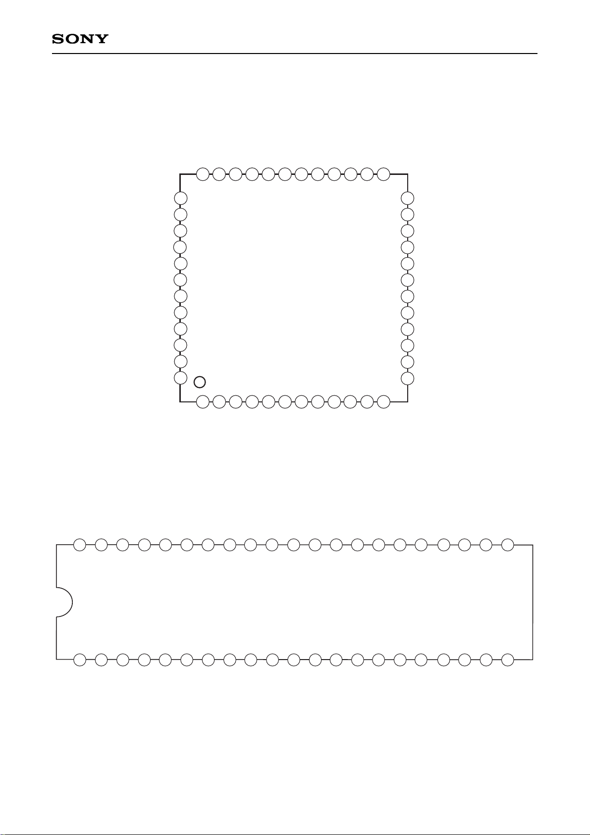
CXA2074Q
48 pin QFP (Plastic)
CXA2074S
42 pin SDIP (Plastic)
– 2 –
CXA2074Q/S
AUX1-L
AUX1-R
VCAWGT
VCATC
VCAIN
VEOUT
VEWGT
VE
SAPIN
SAPOUT
STIN
SUBOUT
V
CC
VETC
NOISETC
TRER
TREL
SDA
SCL
DGND
MAININ
MAINOUT
PCINT2
PLINT
COMPIN
VGR
IREF
GND
SAPTC
PCINT1
BASSR1
BASSR2
BASSL1
BASSL2
LSOUT-R
LSOUT-L
LPIN-L
LPIN-R
LPOUT-L
AUX2-L
AUX2-R
LPOUT-R
1
2
3
4
5
6
7
8
9
10
11
12
13
14 15
16
17
18
19
20
21
22
23
24
25
26
27
28
29
30
31
32
33
34
35
36
37
38
39
40
41
42
Pin Configuration (Top View)
CXA2074Q
CXA2074S
25
26
27
28
29
30
36
35
34
31
32
33
AUX1-L
AUX1-R
NC
VCAWGT
VCATC
VCAIN
VEOUT
NC
VETC
VEWGT
VE
SAPIN
2
3
4
5
6
7
8
9
10
11
121
TREL
LSOUT-R
LSOUT-L
SCL
DGND
NC
PCINT2
NC
MAINOUT
MAININ
SDA
PCINT1
13
14
15
16
17
18
19
20
21
22
23
24
PLINT
COMPIN
IREF
GND
SAPTC
NC
STIN
NOISETC
VGR
V
CC
SAPOUT
SUBOUT
40
39
38
37
41
42
43
44
45
46
47
48
TRER
BASSL2
BASSL1
BASSR2
LPOUT-L
BASSR1
LPIN-L
LPIN-R
LPOUT-R
AUX2-L
AUX2-R
NC
– 3 –
CXA2074Q/S
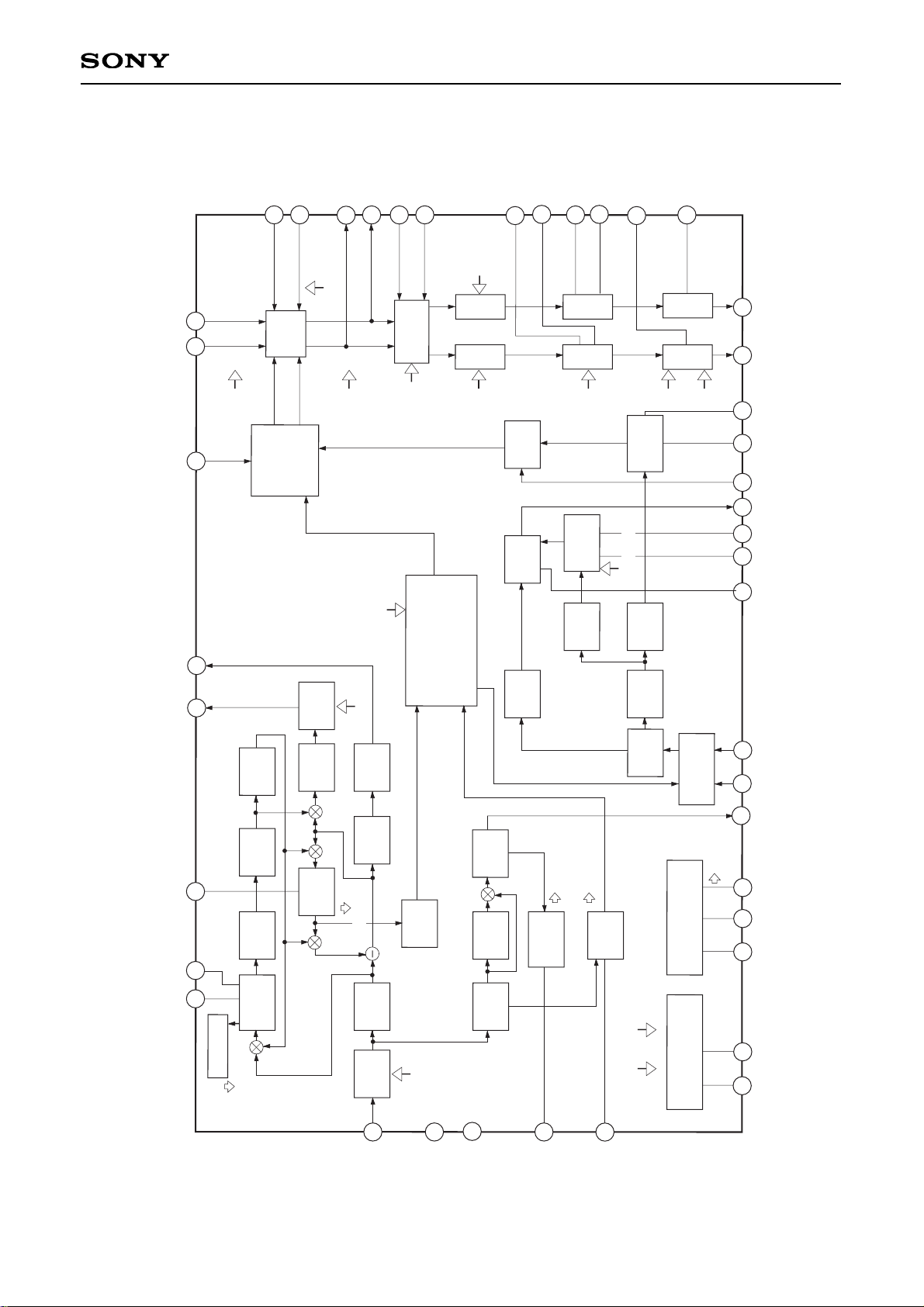
Block Diagram
CXA2074Q
VGR
IREF
DGND
SCL
SDA
SAPOUT
SAPIN
STIN
VE
VEWGT
VETC
VEOUT
VCAIN
VCAWGT
VCATC
MAININ
MAINOUT
SUBOUT
PLINT
PCINT1
COMPIN
V
CC
GND
NOISETC
SAPTC
AUX2-L
IREF
SW
LPF LPF
HPF
RMSDET
RMSDET
VCAVEDeEm
LOGIC
MATRIX
VCA
LPF
LPF
1/21/4VCOLFLT
STLPF
"FILTER"
VCA LPF
BPF
SAPVCO
LPF
NOISE
DET
SAPIND
"PONRES"
STIND
"SAP"
"NOISE"
VCO
NRSW/FOMO/SAPC
WIDEBAND
SPECTRAL
"STEREO"
DeEm
FLT
AMP
(+4dB)
I
2
C BUS I/F
(+6dB)
LSOUT-L
LSOUT-R
M2
TREBLE
TREB
TREB
BASS
PASSSW
BASS
BASS
AUX1-R
AUX1-L
AUX2-R
BASSL1
BASSL2
BASSR1
BASSR2
FILTER
PCINT2
VOL-R
VOL-L
VOL-L
TVSW
LPIN-L
LPIN-R
LPOUT-L
LPOUT-R
FEXT2
FEXT1
TVSW/EXT/M1
TREL
TRER
VOL-R
36
35
38
37
40
39
42
41
ATT
2
3
32
33
31
30
28
2726
48
1
45
44
47
46
8
9
21
13
12
11
14
19
17
23
18
15
16
6
5
4
24
25
22
PSW
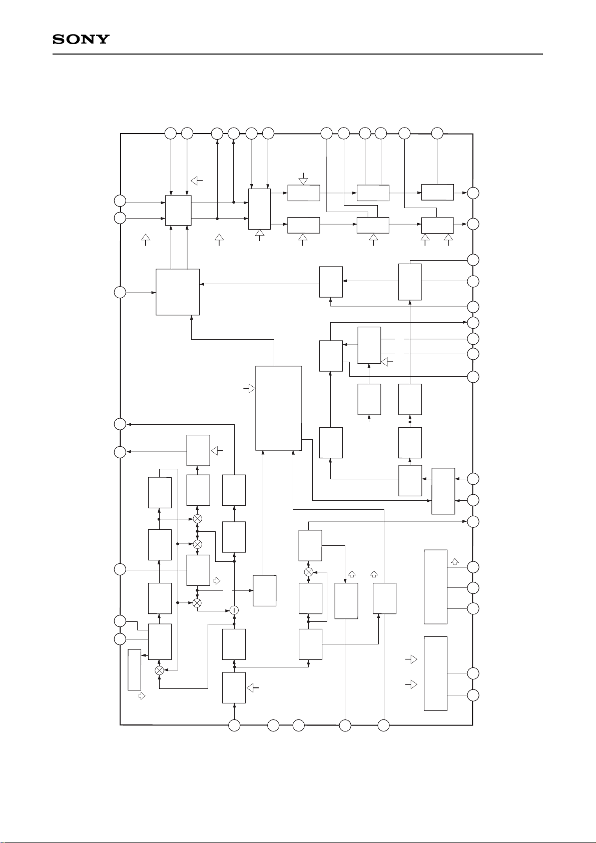
VGR
IREF
DGND
SCL
SDA
SAPOUT
SAPIN
STIN
VE
VEWGT
VETC
VEOUT
VCAIN
VCAWGT
VCATC
MAININ
MAINOUT
SUBOUT
PLINT
PCINT1
COMPIN
V
CC
GND
NOISETC
SAPTC
AUX2-L
HPF
RMSDET
1/21/4VCOLFLT
"FILTER"
"PONRES"
"SAP"
"NOISE"
NRSW/FOMO/SAPC
WIDEBAND
SPECTRAL
"STEREO"
(+6dB)
LSOUT-L
LSOUT-R
M2
TREBLE
TREB
TREB
BASS
BASS
BASS
AUX1-R
AUX1-L
AUX2-R
BASSL1
BASSL2
BASSR1
BASSR2
PCINT2
VOL-R
VOL-L
VOL-L
IREF
SW
LPF LPF
RMSDET
VCAVEDeEm
LOGIC
MATRIX
VCA
LPF
LPF
STLPF
VCA LPF
BPF
SAPVCO
LPF
NOISE
DET
SAPIND
STIND
VCO
DeEm
FLT
AMP
(+4dB)
I
2
C BUS I/F
PASSSW
FILTER
TVSW
LPIN-L
LPIN-R
LPOUT-L
LPOUT-R
FEXT2
FEXT1
TVSW/EXT/M1
TREL
TRER
VOL-R
3
4
1
2
8
7
ATT
6
5
33
32
34
31
30
29
28
24
27
26
18
19
11
10
9
14
15
16
23
13
12
36
35
17
22
20
25
21
38
37
39
42
41
40
PSW
– 4 –
CXA2074Q/S
CXA2074S
– 5 –
CXA2074Q/S
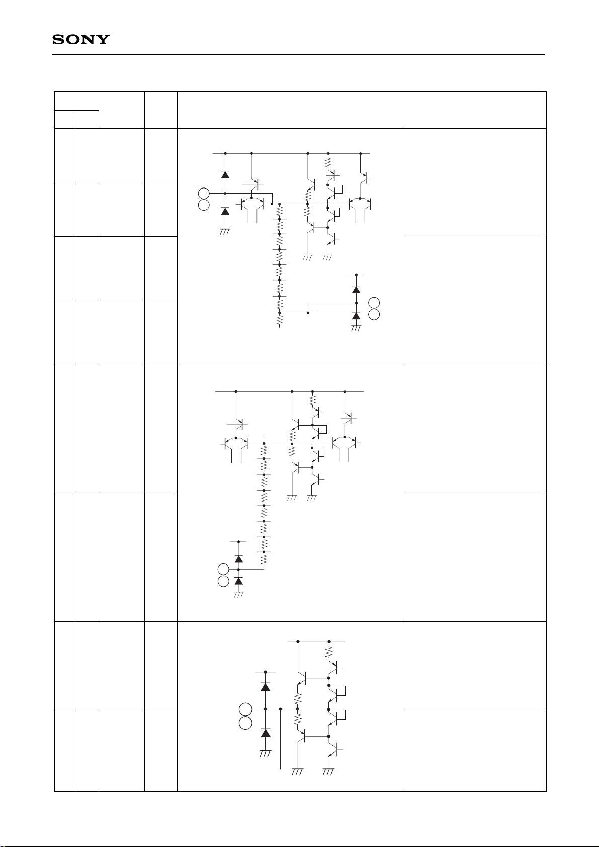
BASSR1
BASSR2
BASSL1
BASSL2
TRER
TREL
LSOUT-R
LSOUT-L
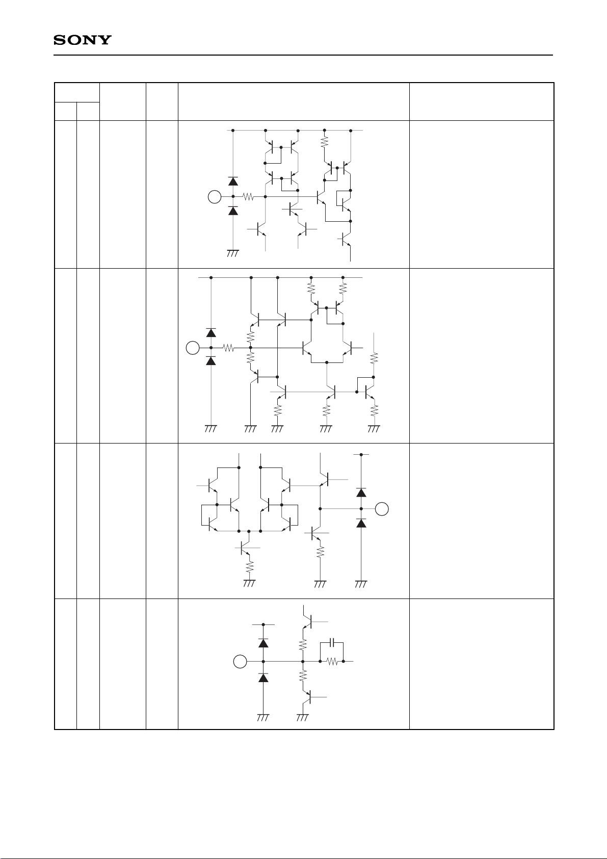
4.0V
4.0V
4.0V
4.0V
4.0V
4.0V
4.0V
4.0V
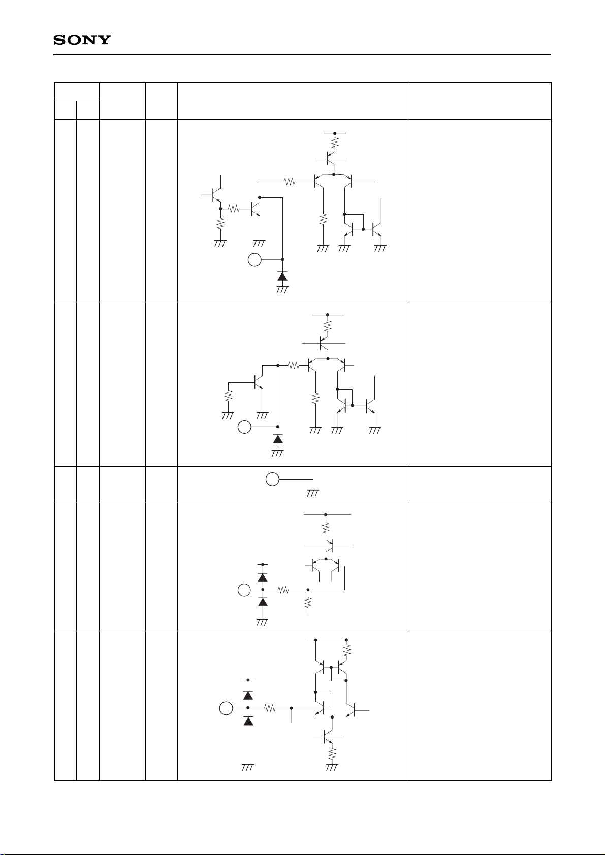
BASS filter pin. (Right channel)
(Connect a 47nF capacitor
between Pins 1 and 2 (44
and 45).)
The cutoff frequency is
determined by the built-in
resistor and the external
capacitance.
BASS filter pin. (Left channel)
(Connect a 47nF capacitor
between Pins 3 and 4 (46
and 47).)
The cutoff frequency is
determined by the built-in
resistor and the external
capacitance.
TREBLE filter pin.
(Right channel)
(Connect a 6.8nF capacitor
between this pin and GND.)
TREBLE filter pin.
(Left channel)
(Connect a 6.8nF capacitor
between this pin and GND.)
LSOUT right channel output
pin.
LSOUT left channel output
pin.
190
190
3k
4V
VCC
4.2k
3.4k
2.7k
2.2k
1.8k
1.4k
1.2k
4.9k
VCC
2
4
1
3
(45)
(47)
(44)
(46)
580
580
3k
VCC
4.2k
3.4k
2.7k
2.2k
1.8k
1.4k
1.2k
4.9k
VCC
5
6
(48)
(1)
580
580
VCC
VCC
3k
7
8
(2)
(3)
44
45
46
47
48
1
2
3
1
2
3
4
5
6
7
8
Pin No.
QFP
SDIP
Symbol
Pin
voltage
Equivalent circuit
Description
Pin Description
– 6 –
CXA2074Q/S
4
5
6
8
9
9
10
11
12
13
SDA
SCL
DGND
MAININ
MAINOUT
—
—
—
4.0V
4.0V
Serial data I/O pin.
VIH >0V
VIL < 1.5V
Serial clock input pin.
VIH >3.0V
VIL < 1.5V
Digital block GND.
Input the (L + R) signal from
MAINOUT (Pin 13 (9)).
(L + R) signal output pin.
7.5k
4.5k
× 5
4k
3k
7.5k
V
CC
↓ 35µ
2.1V
× 2
9
(4)
7.5k
↓ 35µ
2.1V
10.5k
× 4
4k
3k
VCC
10
(5)
11
(6)
VCC
147
10k
53k
4V
VCC
12
(8)
VCC
147
1k
15k
↓
200µ
V
CC
× 4
13
(9)
Pin No.
QFP
SDIP
Symbol
Pin
voltage
Equivalent circuit
Description
– 7 –
CXA2074Q/S
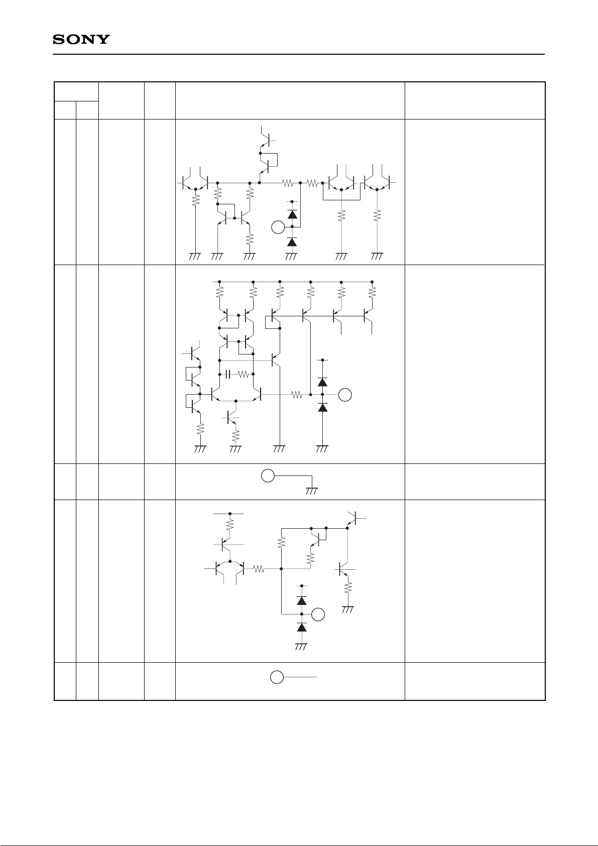
11
12
13
14
14
15
16
17
PCINT1
PCINT2
PLINT
COMPIN
4.0V
4.0V
5.1V
4.0V
Stereo block PLL loop filter
integrating pin.
Pilot cancel circuit loop filter
integrating pin.
(Connect a 1µF capacitor
between this pin and GND.)
Audio multiplexing signal
input pin.
VCC
147
20k
↓
26µ
20k
10k
20k
↓
50µ
20k
20k
16
(13)
VCC
22k
3V
20k
4k 4k 4k 16k
24k
50k 147
3k
17
(14)
22k
VCC
30k
147
14
(11)
4k
VCC
× 2
10k
10k
2k
147
15
(12)
Pin No.
QFP
SDIP
Symbol
Pin
voltage
Equivalent circuit
Description
– 8 –
CXA2074Q/S
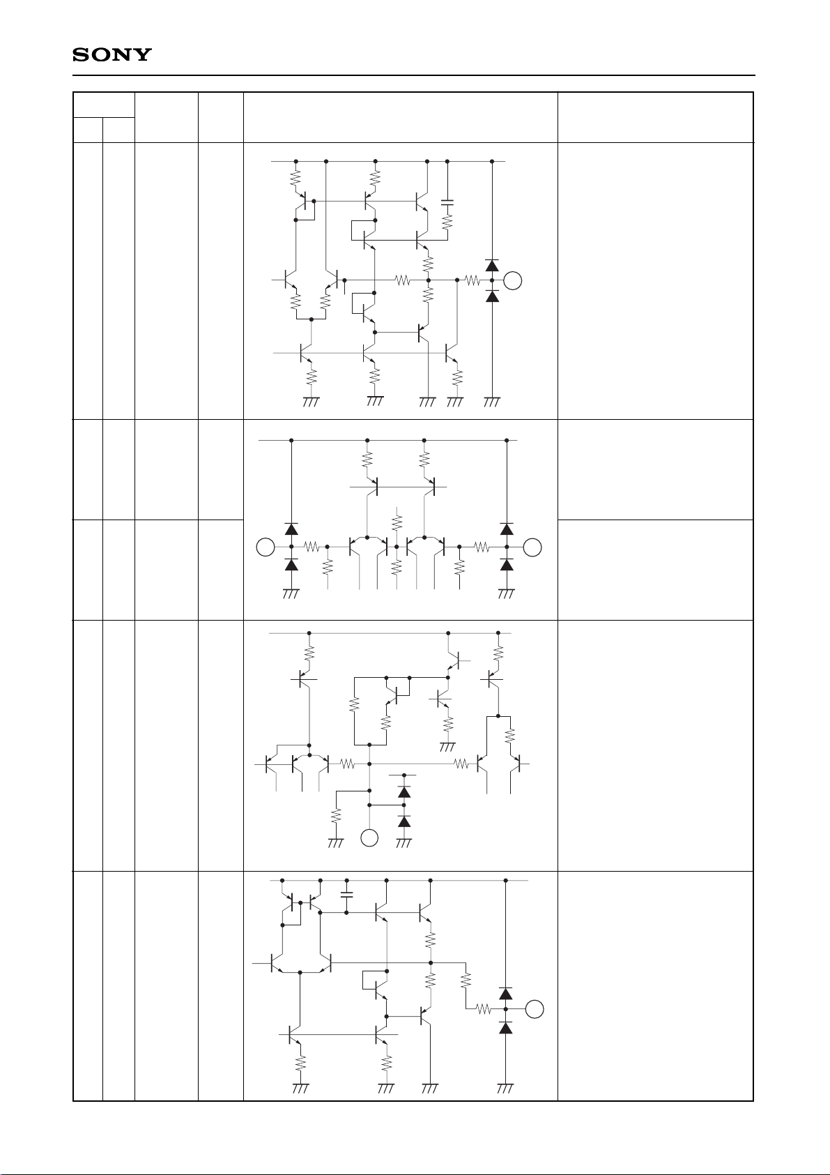
15
16
17
18
19
18
19
20
21
22
VGR
IREF
GND
SAPTC
VCC
1.3V
1.3V
—
4.5V
—
Band gap reference output
pin.
(Connect a 10µF capacitor
between this pin and GND.)
Set the filter and VCO
reference current. The
reference current is adjusted
with the BUS DATA based
on the current which flows to
this pin.
(Connect a 62kΩ (±1%)
resistor between this pin and
GND.)
Analog block GND.
Set the time constant for the
SAP carrier detection circuit.
(Connect a 4.7µF capacitor
between this pin and GND.)
Supply voltage pin.
8k
4k
3k
10k
V
CC
↓ 50µ
1k
VCC
21
(18)
22
(19)
20
(17)
40k 40k 30k
30p 1.8k
16k
6.3k
147
30k 15k 30k
VCC
× 2
V
CC
19
(16)
× 4
11k
9.7k
19.4k
2.06k
3k
147
VCC
11k
11k
18
(15)
Pin No.
QFP
SDIP
Symbol
Pin
voltage
Equivalent circuit
Description
– 9 –
CXA2074Q/S
21
22
25
23
24
23
24
27
25
26
SUBOUT
STIN
SAPIN
NOISETC
SAPOUT
4.0V
4.0V
4.0V
3.0V
4.0V
(L – R) signal output pin.
Input the (L – R) signal from
SUBOUT (Pin 23 (21)).
Input the (SAP) signal from
SAPOUT (Pin 26 (24)).
Set the time constant for the
noise detection circuit.
(Connect a 4.7µF capacitor
between this pin and GND.)
SAP FM detector output pin.
23k
147
18k
20k
11.7k
23k
4V
147
18k
4V
VCC
24
27
(22) (25)
3k
3k
3.3k
4k
4V
Vcc
8k
× 2
10k
1k
2k
Vcc
25
200k
(23)
24k
↓ 10µ
580
Vcc
5P
580
4k
↓ 50µ
10k
147
26
(24)
Pin No.
QFP
SDIP
Symbol
Pin
voltage
Equivalent circuit
Description
2k 2k
2k
2k2k
14.4k
4k
580
580
10P
4k
147
1k
Vcc
23
(21)
– 10 –
CXA2074Q/S
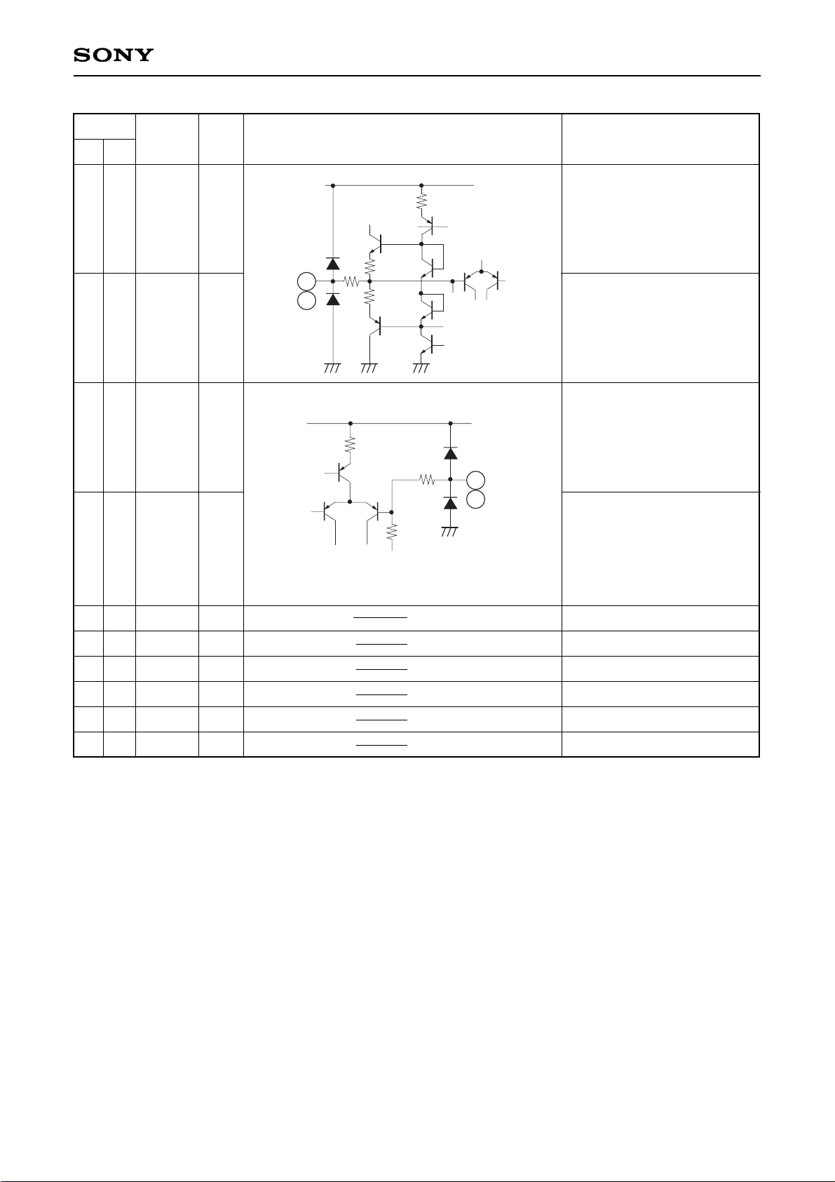
26
27
28
30
28
29
30
31
VE
VEWGT
VETC
VEOUT
4.0V
4.0V
1.7V
4.0V
Variable de-emphasis
integrating pin.
(Connect a 2700pF capacitor
and a 3.3kΩ resistor in series
between this pin and GND.)
Weight the variable
de-emphasis control
effective value detection
circuit.
(Connect a 0.047µF
capacitor and a 3kΩ resistor
in series between this pin
and GND.)
Determine the restoration
time constant of the variable
de-emphasis control
effective value detection
circuit.
(The specified restoration
time constant can be
obtained by connecting a
3.3µF capacitor between this
pin and GND.)
Variable de-emphasis output
pin.
(Connect a 4.7µF non-polar
capacitor between Pins 31
(30) and 32 (31).)
Vcc
4V
36k
2.9V
580
147
580
8k
30k
↓ 8µ
4k
↓ 50µ
29
(27)
20k
↓ 7.5µ
4k
↓ 50µ
Vcc
× 4
× 4
30
(28)
Vcc
10k
580
580
5P
31
(30)
7.5k
147
VCC
28
(26)
Pin No.
QFP
SDIP
Symbol
Pin
voltage
Equivalent circuit
Description
– 11 –
CXA2074Q/S
31
32
33
35
36
37
38
32
33
34
35
36
37
38
VCAIN
VCATC
VCAWGT
AUX1-R
AUX1-L
AUX2-R
AUX2-L
4.0V
1.7V
4.0V
4.0V
4.0V
4.0V
4.0V
VCA input pin.
Input the variable
de-emphasis output signal
from Pin 31 (30) via a
coupling capacitor.
Determine the restoration
time constant of the VCA
control effective value
detection circuit.
(The specified restoration
time constant can be
obtained by connecting a
10µF capacitor between this
pin and GND.)
Weight the VCA control
effective value detection
circuit.
(Connect a 1µF capacitor
and a 3.9kΩ resistor in series
between this pin and GND.)
Right channel external input
1 pin.
Left channel external input
1 pin.
Right channel external input
2 pin.
Left channel external input
2 pin.
4k
VCC
30k 8k
36k
2.9V
3p
580
580
147
40k 40k
↓
50µ
↓
8µ
34
(33)
↓
50µ
VCC
4k
20k
× 4
× 4
↓
7.5µ
33
(32)
VCC
20k
VCC
47k
47k
32
(31)
VCC
4V
27.5k
47k
147
10k
35
36
37
38
Pin No.
QFP
SDIP
Symbol
Pin
voltage
Equivalent circuit
Description
– 12 –
CXA2074Q/S
39
40
41
42
7
10
20
29
34
43
39
40
41
42
—
—
—
—
—
—
LPOUT-R
LPOUT-L
LPIN-R
LPIN-L
NC
NC
NC
NC
NC
NC
4.0V
4.0V
4.0V
4.0V
—
—
—
—
—
—
LPOUT right channel output
pin.
LPOUT left channel output
pin.
Right channel loop input pin.
Left channel loop input pin.
VCC
4V
47k
147
10k
41
42
3k
580
580
VCC
39
40
147
Pin No.
QFP
SDIP
Symbol
Pin
voltage
Equivalent circuit
Description
(7)
(10)
(20)
(29)
(34)
(43)
 Loading...