

Sony CXA2067S Datasheet
—1—
E99213
Sony reserves the right to change products and specifications without prior notice. This information does not convey any license by
any implication or otherwise under any patents or other right. Application circuits shown, if any, are typical examples illustrating the
operation of the devices. Sony cannot assume responsibility for any problems arising out of the use of these circuits.
Absolute Maximum Ratings (Ta=25 °C, GND=0 V)
• Supply voltage VCC/R/G/B 14 V
VCC 7V
•Operating temperature Topr –20 to +75 °C
• Storage temperature Tstg –65 to +150 °C
• Allowable power dissipation
PD 2.05 W
Recommended Operating Conditions
Supply voltage VCC/R/G/B 12±0.5 V
VCC 5±0.5 V
Description
The CXA2067S is a bipolar IC developed for high-
resolution computer displays.
Features
• Wide-band amplifier: 170 MHz@–3 dB (Typ)
• Input dynamic range: 1.0 Vp-p (typ)
• High gain preamplifier (17 dB)
• R, G and B in a single package (SDIP 30 pins)
• I2C bus control
Contrast control
Sub contrast control
Brightness control
OSD contrast control
Cut-off control: 4 channels of DAC output
2 blanking level modes
(0.5 V fixed, pedestal –0.3 V)
• Sync separator for sync-on-green
• Blanking mixing function
• OSC mixing function
• Video interval detection function
• VBLK sync DAC refresh system
• 12 V power supply interlocked power saving
function
Applications
High-resolution computer displays
Structure
Bipolar silicon monolithic IC
Preamplifier for High-Resolution Computer Display
30 pin SDIP (Plastic)
CXA2067S
—2—
CXA2067S
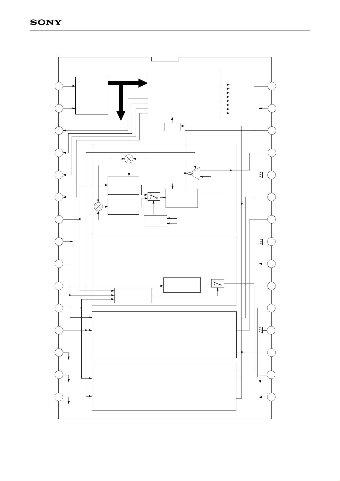
LPF
SDA
SCL
COF R
COF G
COF B
COF RGB
RIN
V
CC
GIN
SYNC IN
BIN
CLP
OSD-R
OSD-G
OSD-B
CSYNC/VDET
V
CC R
S/H-R
ROUT
GND-R
S/H-G
GOUT
GND-G
V
CC G
S/H-B
BOUT
GND-B
BLKING
YS
V
CC B
to
OSDSW
to
OSDSW
to
OSDSW
to
OSDSW
Rch
Bch
OSD YS
GENERATOR
GAIN
CONTROL
AMP
GAIN CONTROL DATA
SYNC SEP/VDET
VDET
COMPARATOR
SYNC
SEPARATOR
SVSW
SUB
CONTRAST
CONTRAST
OSD SW
BLANKING
MODE
BLANKING PULSE
BRIGHTNESS
OSD GAIN (R)
OSD PULSE (13PIN)
YS PULSE (17PIN)
To each MODE SW
I C BUS
DECORDER
2
BLANKING
BUFFER AMP
Same as R channel
Same as R channel
Gch
17
18
19
20
21
23
24
25
26
27
28
29
30
1
2
3
4
5
6
7
8
9
10
11
12
13
14
15
12V
5V
12V
12V
22
16
D/A CONVERTOR
CONTRAST
SUB CONTRAST (R)
SUB CONTRAST (G)
SUB CONTRAST (B)
OSD GAIN (R)
OSD GAIN (G)
OSD GAIN (B)
BRIGHTNESS (RGB)
CUTOFF (R)
CUTOFF (G)
CUTOFF (B)
CUTOFF (RGB)
Block Diagram

—3—
CXA2067S
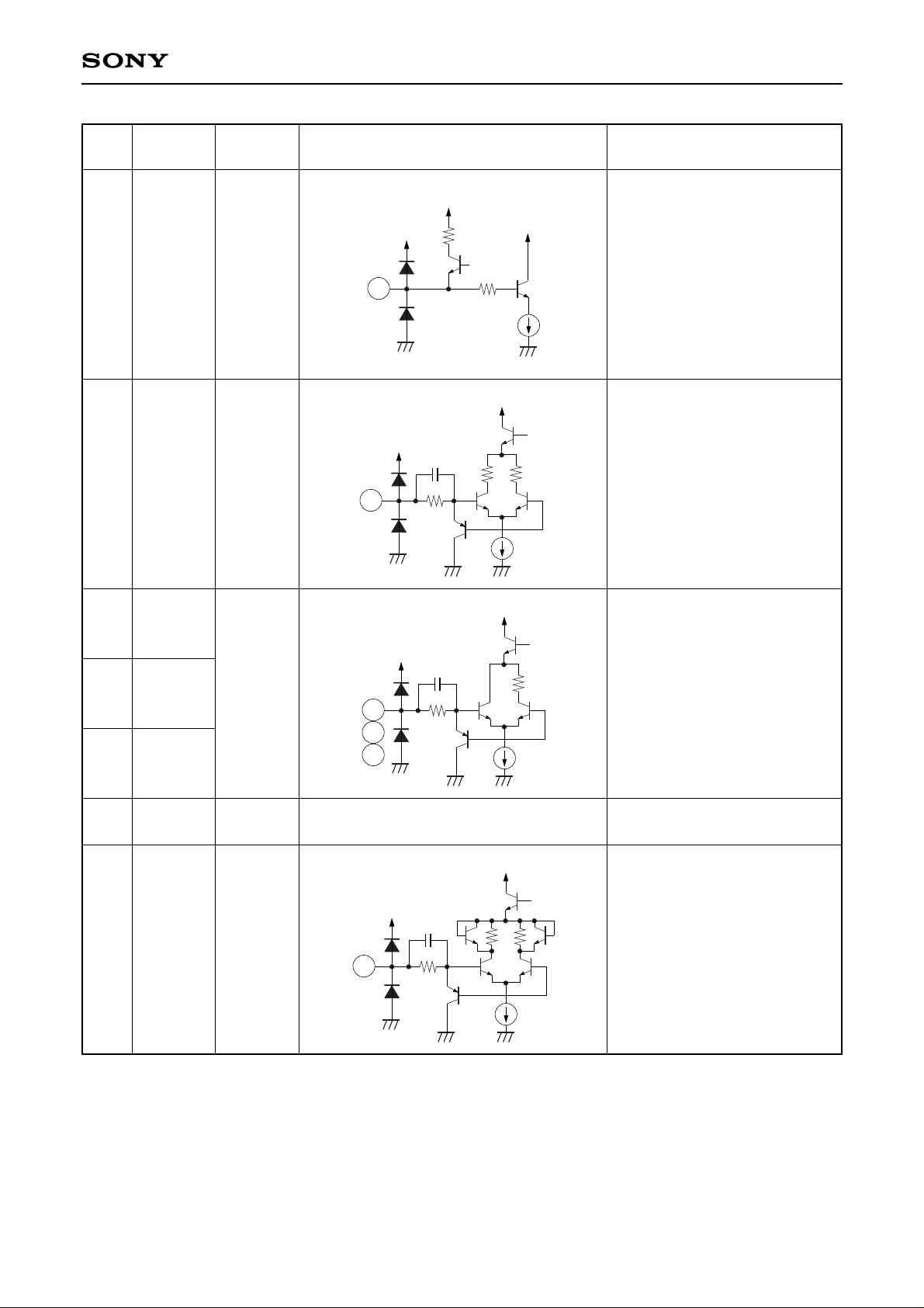
Pin Description
1
2
3
4
5
6
7
9
11
8
SDA
SCL
COF R
COF G
COF B
COF RGB
RIN
GIN
BIN
VCC
—
—
—
1.7 V
(Clamp)
5 V
1
4k
VCC
4k
10k
VCC
2
100
VCC
VCC
3
4
5
6
VCC
1k
1k
VCC
VCC
VCC VCC
14k
V
CC
8k
V
CC
7
9
300
11
I2C bus standard SDA
(serial data) input/output.
VILMAX=1.5 V
VIHMIN=3.5 V
VOLMAX=0.4 V
I2C bus standard SCL
(serial clock) input/output.
VILMAX=1.5 V
VIHMIN=3.5 V
DAC output for cut-off
adjustment.
Output DC is 1 to 4 V.
R, G and B signal inputs.
Input via a capacitor.
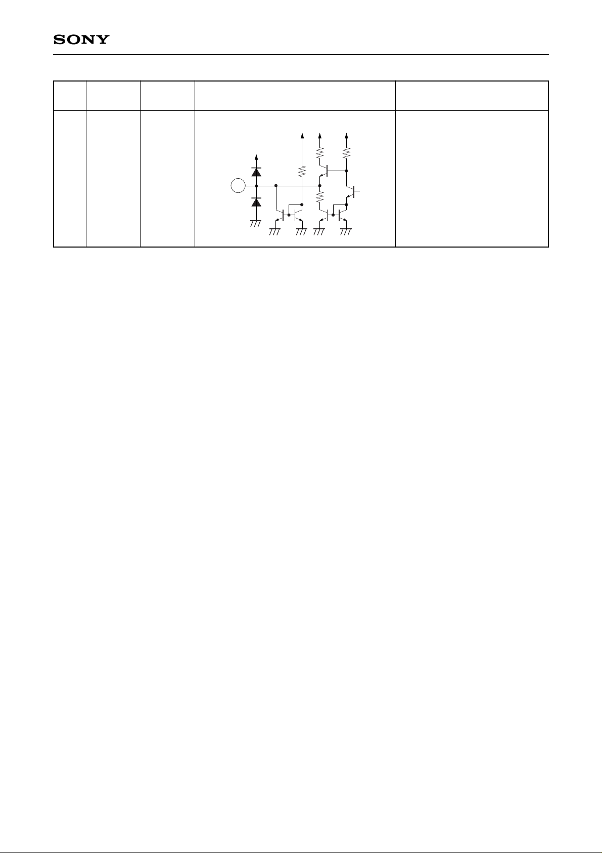
5 V power supply.
Pin
Symbol
Pin
Equivalent circuit Description
No. voltage
—4—
CXA2067S
10
12
13
14
15
16
17
SYNC IN
CLP
OSD-R
OSD-G
OSD-B
VCC B
YS
2.8 V
—
—
12 V
—
100
VCC
VCC
VCC
150
10
VCC
VCC
10k
2p
10k10k
12
VCC
VCC
10k
2p
13
14
15
5k
VCC
VCC
10k
2p
5k
17
Sync-on-green signal input.
Input via a capacitor.
Clamp pulse (positive polarity)
input.
VILMAX=0.8 V
VIHMIN=2.8 V
OSD control inputs.
VILMAX=0.8 V
VIHMIN=2.8 V
12 V power supply. (B channel)
YS (OSD BLK) control input.
VILMAX=0.8 V
VIHMIN=2.8 V
Pin
Symbol
Pin
Equivalent circuit Description
No. voltage
—5—
CXA2067S
18
19
23
26
20
24
27
21
25
28
22
29
BLKING
GND-B
GND-G
GND-R
BOUT
GOUT
ROUT
S/H-B
S/H-G
S/H-R
VCC G
VCC R
—
0 V
—
—
12 V
12 V
VCC VCC
VCC
10k
30k
4k
18
VCCR/G/B
2p
310
5k
20
24
27
VCCR/G/B VCCR/G/B
1k
VCC
VCC
VCC
1k
300
21
25
28
Blanking pulse input.
Set the V blanking pulse width
to 300 µs or more.
VILMAX=0.8 V
VIHMIN=2.8 V
Ground.
R, G and B outputs.
Brightness sample-and-hold.
Connect to GND via a capacitor.
12 V power supply. (G channel)
12 V power supply. (R channel)
Pin
Symbol
Pin
Equivalent circuit Description
No. voltage
—6—
CXA2067S
30
CSYNC
/VDET
—
VCC VCC
VCC
500
100
VCC
5k
20k
30
Sync-on-green signal sync
separator output/video detector
output.
Either of them is selected by
SVSW of I2C bus.
Typ. : High=4.3 V
Low=0.2 V
(positive polarity)
Pin
Symbol
Pin
Equivalent circuit Description
No. voltage
 Loading...