

Sony CXA2066S Datasheet

Description
The CXA2066S is a bipolar IC developed for high
resolution computer displays.
Features
• Built-in wide band amplifier: 140MHz @ –3dB (Typ.)
• Input dynamic range: 1.0Vp-p (Typ.)
• High gain preamplifier (17dB)
• R, G, and B incorporated in a single package
• I2C bus control
Contrast control
Subcontrast control
Brightness control
OSD contrast control
Cutoff control 4-channel DAC output
2 blanking level modes (0.5V fixed and Pedestal –0.6V)
ABL control pin
• Built-in sync separator for Sync on Green
• Built-in blanking mixing function
• Built-in OSD mixing function
• Video period detection function
• Built-in sharpness function
• Built-in VBLK synchronous DAC refresh system
Applications
High resolution computer displays
Structure
Bipolar silicon monolithic IC
Absolute Maximum Ratings (Ta = 25°C, GND = 0V)
• Supply voltage VCC 14 V
VCC27 V
• Operating temperature Topr –20 to +75 °C
• Storage temperature Tstg –65 to +150 °C
• Allowable power dissipation PD 2.05 W
Recommended Operating Conditions
Supply voltage VCC 12 ± 0.5 V
VCC2 5 ± 0.5 V
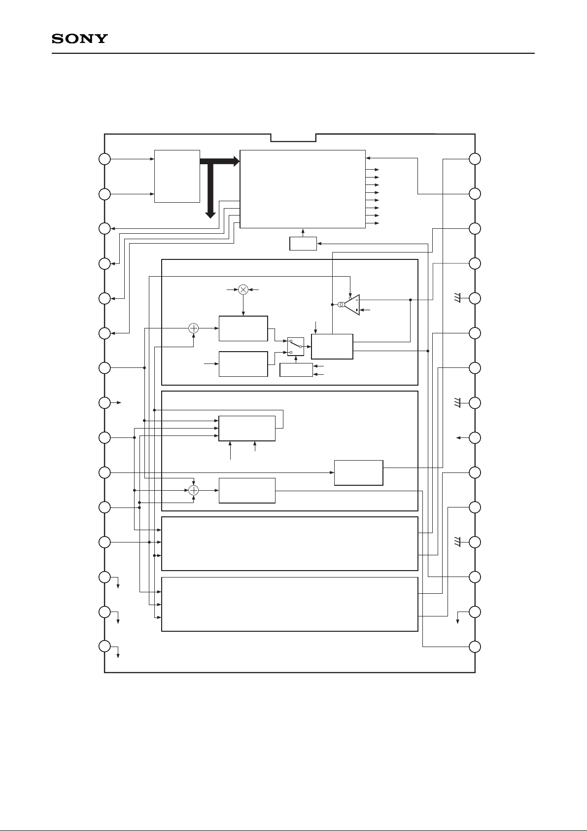
CXA2066S
Preamplifier for High Resolution Computer Display
– 1 –
E98210-PS
Sony reserves the right to change products and specifications without prior notice. This information does not convey any license by
any implication or otherwise under any patents or other right. Application circuits shown, if any, are typical examples illustrating the
operation of the devices. Sony cannot assume responsibility for any problems arising out of the use of these circuits.
30 pin SDIP (Plastic)
– 2 –
CXA2066S
3
4
5
6
7
8
9
10
11
OSD-G
OSD-B
SDA
SCL
COF R
COF G
COF B
COF RGB
RIN
V
CC2
GIN
SYNC IN
BIN
CLP
OSD-R
D/A CONVERTER
I
2
C BUS
DECORDER
CUTOFF (R)
CUTOFF (G)
CUTOFF (B)
CUTOFF (RGB)
LPF
OSD GAIN (R)
OSD GAIN (G)
OSD GAIN (B)
BRIGHTNESS (RGB)
BRIGHTNESS
SUB CONTRAST (R)
SUB CONTRAST (G)
SUB CONTRAST (B)
CONTRAST
OSD SW
GAIN
CONTROL
AMP
GAIN CONTROL
DATA
CONTRAST
Rch
SUB
CONTRAST
BLANKING
BUFFER
AMP
BLANKING PULSE
BLANKING
MODE
OSD YS
GENERATOR
OSD GAIN (R)
Gch
5V
to
OSDSW
Same as R channel
To each MODE switch
Bch
Same as R channel
VDET, SYNC SEP, SHARPNESS
SHARPNESS
GAIN CONT.
T SW
SYNC
SEPARATOR
12V
OSD PULSE (13PIN)
YS PULSE (17PIN)
VDET
COMPARATOR
to
OSDSW
to
OSDSW
to
OSDSW
1
2
13
14
15
12
16
17
18
19
20
21
22
23
24
25
26
27
28
S/H-R
29
ABL
30
CSYNC
ROUT
GND-R
S/H-G
GOUT
GND-G
V
CC
S/H-B
BOUT
GND-B
BLKING
YS
VDET
Block Diagram
– 3 –
CXA2066S
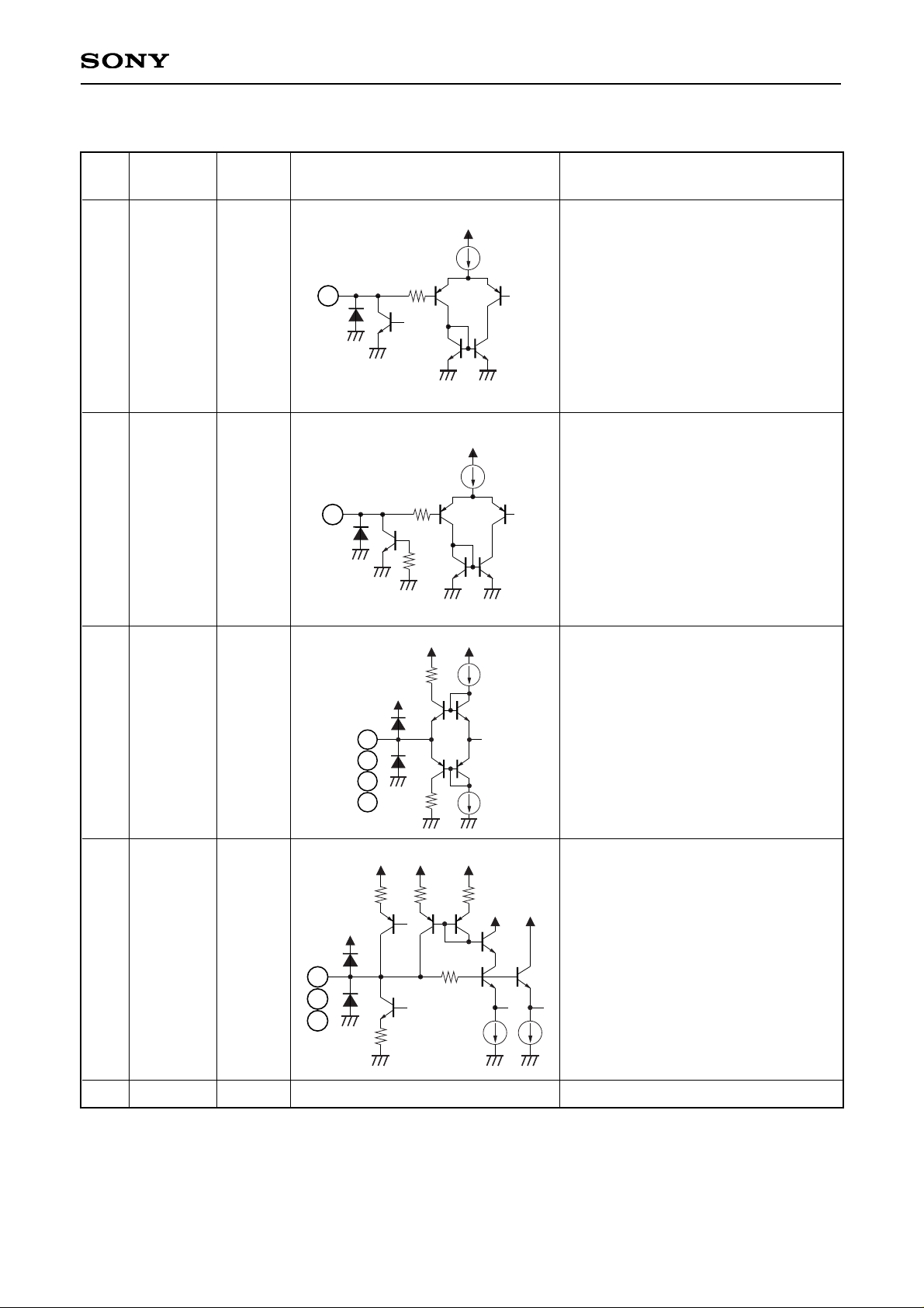
Pin Description
Pin
No.
Symbol
SDA
1
Equivalent circuit
Description
I2C bus standard SDA (serial data)
input/output.
VILMAX = 1.5V
VIHMIN = 3.5V
VOLMAX = 0.4V
Pin
voltage
1
VCC
4k
SCL
2
I2C bus standard SCL (serial clock)
input.
VILMAX = 1.5V
VIHMIN = 3.5V
2
VCC
4k
10k
COF R
COF G
COF B
COF RGB
3
4
5
6
Cut-off adjustment DAC outputs.
The output DC is 1 to 4V.
3
4
5
6
VCCVCC
VCC
100
RIN
GIN
BIN
VCC2 5V
1.7V
(when
clamped)
7
9
11
8
RGB signal inputs.
Input via the capacitor.
5V power supply.
7
9
11
VCC
VCC
1k
1k
VCC
14k
VCC
VCC
8k
300
VCC

– 4 –
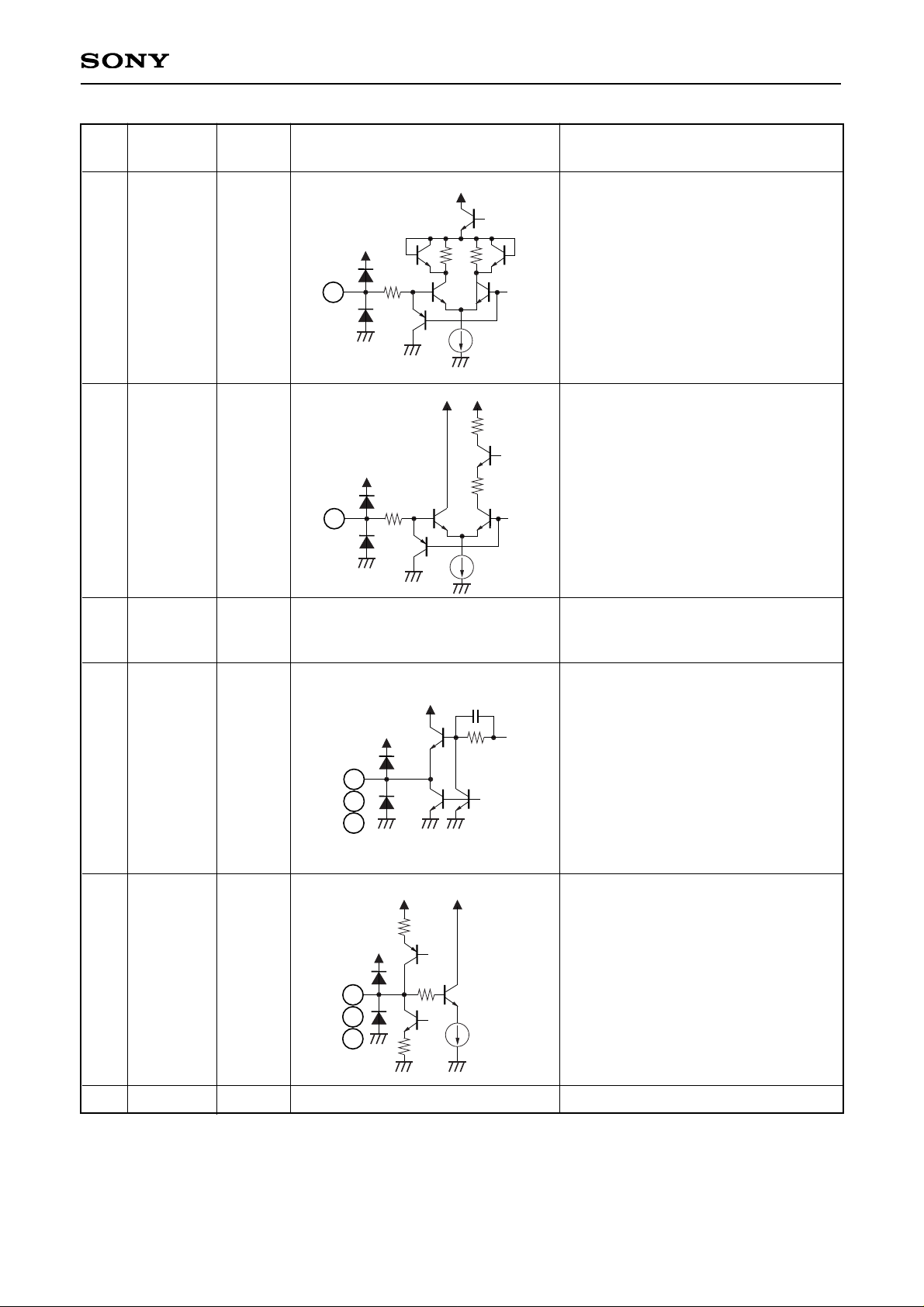
CXA2066S
Pin
No.
Symbol
SYNC IN
10
Equivalent circuit
Description
Sync on Green signal input.
Input via the capacitor.
Pin
voltage
10
VCC
VCC
100
150
VCC
CLP
12
Clamp pulse (positive polarity) input.
VILMAX = 0.8V
VIHMIN = 2.8V
12
VCC
VCC
10k
10k10k
OSD-R
OSD-G
OSD-B
13
14
15
OSD control inputs.
VILMAX = 0.8V
VIHMIN = 2.8V
13
14
15
VCC
VCC
10k
5k
VDET
16
Video detector output.
Typ.; High = 4.3V
Low = 0.2V
16
VCC2
100
VCC2
5k
VCC2
20k
VCC2
2.8V
– 5 –
CXA2066S
Pin
No.
Symbol
YS
17
Equivalent circuit
Description
YS (OSD_BLK) input.
VILMAX = 0.8V
VIHMIN = 2.8V
Pin
voltage
17
VCC
VCC
10k
5k
BLKING
18
Blanking pulse input.
Set the V blanking pulse width to
300µs or more.
VILMAX = 0.8V
VIHMIN = 2.8V
18
VCC
VCCVCC
10k
30k
4k
GND-B
GND-G
GND-R
19
23
26
GNDs.
BOUT
GOUT
ROUT
VCC 12V
0V
20
24
27
22
R, G, and B signal outputs.
12V power supply.
20
24
27
620
0.5p
VCC
VCC
S/H-B
S/H-G
S/H-R
21
25
28
Brightness sample-and-hold. Connect
a capacitor to GND.
VCC VCC
300
VCC
1k
1k
21
25
28
– 6 –
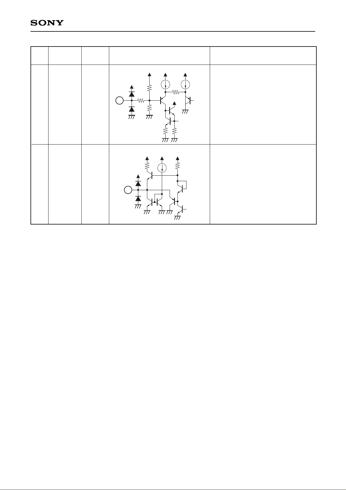
CXA2066S
Pin
No.
Symbol
Equivalent circuit
Description
Pin
voltage
CSYNC
30
Sync on Green signal sync separator
output (positive polarity).
Typ.; High = 4.3V
Low = 0.2V
15k
VCC2 VCC2VCC2
100
VCC2
30
ABL
29
ABL control input.
Ground to GND when not using ABL.
29
VCC
VCC
VCC
VCC
50k
25k
25k
VCC

– 7 –
CXA2066S
I2C BUS Register Definitions
Slave Address
SLAVE RECEIVER; 40 (HEX)
Register Table
SUB ADDRESS BIT7
00H CONTRAST
01H 0
BLK
MODE
BRIGHTNESS
02H CUT OFF R
03H CUT OFF G
04H CUT OFF B
OSD GAIN05H VDET LEVEL
06H CUT OFF RGB
07H SUB CONTRAST R
08H SUB CONTRAST G
09H SUB CONTRAST B
0AH
V DET
OFF
SHP
OFF
SYNC
OFF
T SW SHP GAIN
BIT6 BIT5 BIT4 BIT3 BIT2 BIT1 BIT0
CONTRAST (8) Controls the gain common to the R, G, and B channels. Since control is
performed by multiplying with SUB CONTRAST, the white balance can
be adjusted by SUB CONTRAST and the luminance can be adjusted by
CONTRAST.
0: Gain minimum (–30dB or less)
255: Gain maximum (+17dB)
BLK MODE (1) Switches the blanking level.
0: Pedestal –0.6V
1: 0.5V fixed
BRIGHTNESS (6) Controls the black level common for the R, G, and B channels.
0: Black level minimum (1V)
63: Black level maximum (3V)
CUT OFF R (8) Controls Pin 3 (COF R) output voltage.
0: Output voltage minimum (1V)
255: Output voltage maximum (4V)
CUT OFF G (8) Controls Pin 4 (COF G) output voltage.
0: Output voltage minimum (1V)
255: Output voltage maximum (4V)
CUT OFF B (8) Controls Pin 5 (COF B) output voltage.
0: Output voltage minimum (1V)
255: Output voltage maximum (4V)
Sub Address
0000
Sub Address
0001
Sub Address
0001
Sub Address
0010
Sub Address
0011
Sub Address
0100
 Loading...