Sony CXA2061S Datasheet

Y/C/RGB/D for NTSC Color TVs
Description
The CXA2061S is a bipolar IC which integrates
the luminance signal processing, chroma signal
processing, RGB signal processing, and sync and
deflection signal processing functions for NTSC
system color TVs onto a signal chip. The IC also
includes deflection processing functions for wide
TVs.
Features
• Reduction in peripheral parts
(ceramic oscillator, AKB sample-and-hold capacitor, etc.)
• I2C bus compatible
• Built-in deflection compensation circuit which is capable of supporting variaus wide modes
• Non-adjusting V oscillator frequency with a countdown system
• Non-interlace display support (even/odd selectable)
• Non-adjusting Y/C filter
• Three sets of CV inputs, two sets of Y/C inputs (can serve as both Y/C and CV inputs), one set of Y/C inputs
supports an external combfilter, two sets of RGB inputs, one set of YUV inputs
• It can be outputted YUV on RGB1 inputs
• Built-in dynamic picture and dynamic color circuits
• Built-in AKB and gamma correction circuits
• FSC output
Applications
Color TVs (4:3, 16:9)
Structure
Bipolar silicon monolithic IC
Abusolute Maximum Ratings (Ta = 25°C, GND1, 2 = 0V)
• Supply voltage VCC1, 2 –0.3 to +12 V
• Operating temperature Topr –20 to +75 °C
• Storage temperature Tstg –65 to +150 °C
• Allowable power dissipation PD 1.5 W
(when mounted on a 50mm × 50mm board)
• Voltages at each pin –0.3 to VCC1, 2 + 0.3 V
Operating Condition
Supply voltage VCC1, 2 9 ± 0.5 V
– 1 –
E97538-PS
Sony reserves the right to change products and specifications without prior notice. This information does not convey any license by
any implication or otherwise under any patents or other right. Application circuits shown, if any, are typical examples illustrating the
operation of the devices. Sony cannot assume responsibility for any problems arising out of the use of these circuits.
CXA2061S
48 pin SDIP (Plastic)

– 2 –
CXA2061S
Block Diagram
5
11
13
14
15
17
18
19
22
23
24
40
35
44
45
46
1
PHASE DET.
<H POSITION>
<AFC BOW>
<AFC AMGLE>
HPROT
<<HNG>>
WIDE SAW FUNC.
<ASPECT>
<SCROLL>
<UPPER VLIN>
<LOWER VLIN>
<V ZOOM>
<V UNDER SCAN>
HD GEN.
<HD W>
VD SAW FUNC.
<VON> <S CORRECTION>
<V SIZE> <V LINEARITY>
<V POSITION> <EHT COMP>
EW PARABOLA FUNC.
<H SIZE> <TRAPEZIUM>
<PIN AMP> <EW DC>
<CORNERPIN>
IREF REG
VPROT
<<VNG>>
VM AMP
(OFF YS/YM)
DAC
SW
I
2
C BUS
DECODER
STATUS I/F
Y/C MIX
RGB CLAMP
CLAMP
DC TRAN
<DC TRAN>
VSAW GEN.
VTIM
COLOR AMP
<COLOR>
<C OFF>
AXIS
<AXIS NTSC>
<AXIS PAL>
EYUV CLAMP
YUV SW
<YSEL>
YUVOUT
<YUVOUT>
DPIC
<DPIC>
<AGING>
CLAMP
RGB 1/2
ABL/PEAK LIM
<ABL MODE>
<ABL VTH>
AKB
<<IKR>>
H TIM GEN.
<H BLK>
<LEFT HBLK>
<RIGHT HBLK>
HSAW GEN.
<HOSC>
(ZAP)
AFC
<AFC GAIN>
<FH HIGH>
<<HLOCK>>
<<HCENT>>
COUNT DOWN
<CD MODE>
<INTERLACE>
LINE COUNTER
V TIM GEN.
<V UNDER SCAN>
SHARPNESS DL
SHARPNESS AMP
<SHARPNESS>
<SHP F0>
<PRE/OVER>
V SYNC SEP
<VSS>
H SYNC SEP
<HSS>
<H MASK>
TRAP + EQ
<TRAP OFF>
ATT
CHROMA SW
Y SW
MONITOR SW
VIDEO SW
<VIDEO SEL>
<S SEL>
Y
COLOR KILLER
<<KILLER ID OFF>>
CHROMA
AMP
ACC DET.
ACC AMP
CHROMA
BPF
<C BPF>
FILTER ALIGNMENT
CAL. by fsc
APC
<HUE>
C VCO DEMOD.
FSC
<FSC SW>
YS1 SW
<RGB SEL>
YM SW
YS2 SW
DYNAMIC COLOR
<DYNAMIC C>
GAMMA AMP
<GAMMA>
CLAMP
BRIGHT CONT.
<BRIGHT>
DRIVE AMP
<R/G/B DRIVE>
CUTOFF CONT.
<R/G/B CUTOFF>
R/G/B BLK
<PON>
<R/G/B ON>
PICTURE AMP
<PICTURE>
47
8
39
38
37
36
25
26
27
28
29
30
31
32
3
21
42
34
10
12
16
33
20
2
4
6
7
9
41
43
TV/C2 IN
C1 IN
CVBS2/Y2 IN
COMB-C IN
COMB-Y IN
MON OUT
CVBS1/Y1 IN
AFC FIL
SCP
V TIM
HP/
HPROTECT
HD
GND1
I REF
REG
V
CC
1
YS2/YM
EW
VD+
VD–
SCL
SDA
R OUT
G OUT
B OUT
IK IN
ABL IN
ABL FIL
B2 IN (B-YOUT)
YS1
B1 IN
G1 IN
R1 IN
G2 IN (R-YOUT)
R2 IN (YOUT)
YUV SW
EY IN
ER-Y IN
VM OUT/
V PROT
EB-Y IN
APED
Y CLAMP
GND2
V
CC
2
FSCOUT
X'tal
APC FIL

– 3 –
CXA2061S
Pin Configuration
2
3
4
5
6
7
8
9
10
11
12
13
14
15
16
17
18
19
20
21
22
23
24
25
26
27
28
29
30
40
39
38
37
36
35
34
31
32
33
41
42
43
44
45
46
47
48
1
APED
C1 IN
ABL IN
CVBS1/Y1 IN
V TIM
MON OUT
COMB-C IN
Y CLAMP
COMB-Y IN
GND1
EW
I REF
VD+
VD–
VM OUT/V PROT
REG
SCP
HP/PROTECT
HD
AFC FIL
IK IN
R OUT
G OUT
B OUT
NC
X'tal
FSCOUT
APC FIL
V
CC2
TV/C2 IN
ABL FIL
CVBS2/Y2 IN
GND2
EB-Y IN
ER-Y IN
EY IN
YUV SW
SDA
SCL
V
CC1
R2 IN
G2 IN
B2 IN
YS2/YM
R1 IN
G1 IN
B1 IN
YS1

– 4 –
CXA2061S
Pin Description
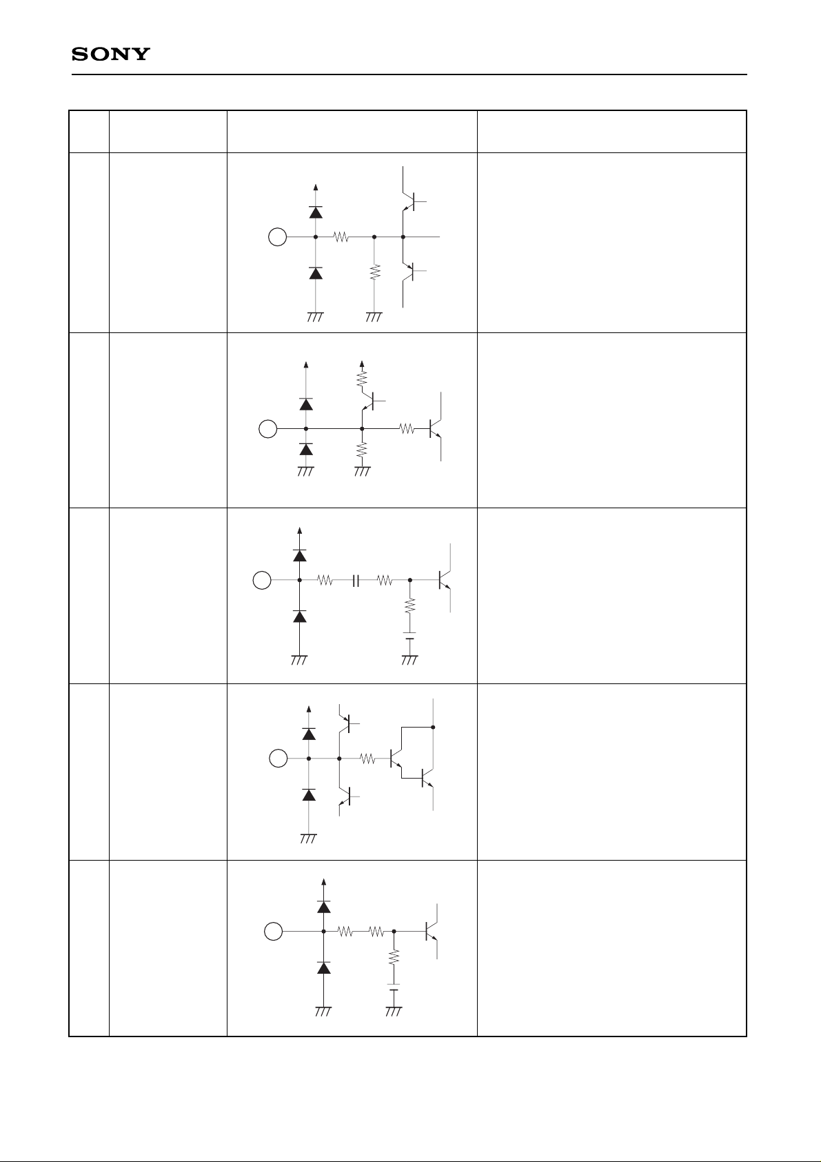
Chroma signal input. Input a chroma
signal with a burst level of 300mVp-p via a
0.1µF capacitor. The S terminal signal is
normally input.
Pin
No.
Symbol Equivalent circuit Description
1
APED
Capacitor connection for black peak hold
of the dynamic picture (black expansion).
Connect to GND via a 4.7µF capacitor.
2
C1 IN
3
ABL IN
ABL control signal input and VD high
voltage fluctuation compensation signal
input. High voltage fluctuation
compensation has linear control
characteristics for the pin voltage range of
about 8 to 1V. Control characteristics can
be varied through EHT COMP control of
the bus. ABL function as PIC/BRT-ABL
(average value type). The threshhold
voltage at which ABL begins to have effect
can be switched between 3 to 1V by the
bus.
4
CVBS1/Y1 IN
CVBS signal/luminance signal input.
Input a 1Vp-p (100% white including sync)
CVBS signal via a 1µF capacitor.
When inputting Y/C separated signal,
input the Y signal.
1
94k
4µA
1k
50k
147
5.4V
2
147
3.7V / 1.7V
3
50k
147
5.4V
4
– 5 –
CXA2061S
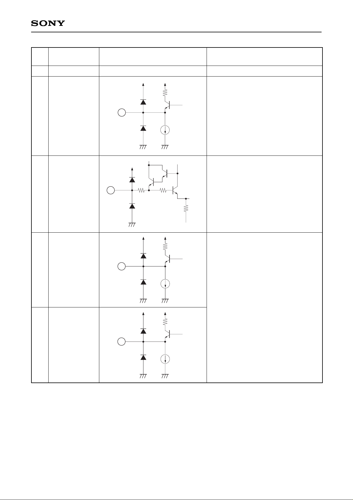
Input the chroma signal from the comb
filter. Standard input level (burst level) is
0.6Vp-p.
Pin
No.
Symbol Equivalent circuit Description
6
MON OUT
The signal input from TV, CVBS1 and
CVBS2 are selected by VIDEO SEL and
S SEL of the bus and output. In the case
of S terminal input, the luminance signal
and chroma signal are mixed and output.
The output level is 2Vp-p including sync.
7
COMB-C IN
8
Y CLAMP
Capacitor connection for luminance signal
clamp.
Connect to GND via a 0.1µF capacitor.
9
COMB-Y IN
Input the luminance signal from the comb
filter. The signal is input via a 0.1µF
capacitor with a level of 2Vp-p.
(100% white including sync)
25.1k
6
200
4K
25k
147
5.4V
25k
7
10p
1.5k
8
25k
147
5.4V
25k
9
5
V TIM
V timing pulse. V timing pulse, HSS and
VSS output can be selected by VTIM SEL
control of the bus.
147
5
25k
– 6 –
CXA2061S
11
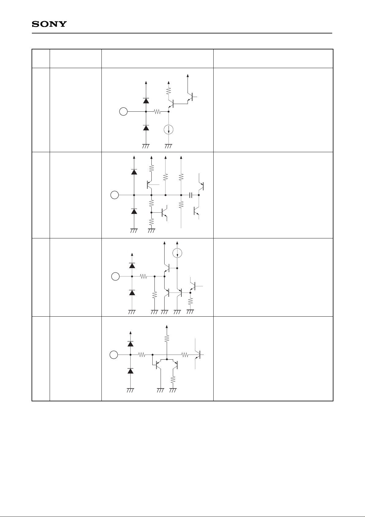
EW V parabola wave output.
1.2k
300µA
11
Pin
No.
Symbol Equivalent circuit Description
12
I REF
Internal reference current setting.
Connect to GND via a 10kΩ resistor
(metal film resistor) with an error of 1% or
less.
13
VD+
14
VD–
V sawtooth wave output. The pin 13 and
14 outputs are the reverse polarity of each
other.
147
7.2k
24k
12
2k
300µA
13
2k
300µA
14
10 GND1
GND (the deflection blocks circuit).
– 7 –
CXA2061S
15
VM OUT/
V PROT
Output the differential waveform of
luminance signal for the VM (Velosity
Modulation) system. This pin is also used
as the V protect signal input.
When a large current (4mA) is pulled from
this pin, the RGB outputs are all blanked
and "1" is output to the status register
VNG.
1k
400µA
147
15
16
REG
Connect decoupling capacitance for
internal regulator. Connect to GND via a
10µF capacitor.
2.2k
16
77k
20k500
160
1k
20pF
H deflection pulse input for H AFC. Input
a 5Vp-p pulse via a capacitor. This pin is
also used as the X-RAY protect signal
Input. If the pin voltage 1V or less for a 7
vertical cycle or longer, then the hold-down
funtion operates. At this time, the HD
output goes to high impedance, the RGB
output are blanked and "1" is output to the
status register HNG. To release this status,
turn the power off and then on again.
Pin
No.
Symbol Equivalent circuit Description
17
SCP
Sand castle pulse output.
The sand castle pulse is the waveform
obtained by superimposing the burst gate
pulse onto the composite blanking pulse.
18
HP/PROTECT
25k
50µA
17
50k
147
147
18
75k
25k
10k

– 8 –
CXA2061S
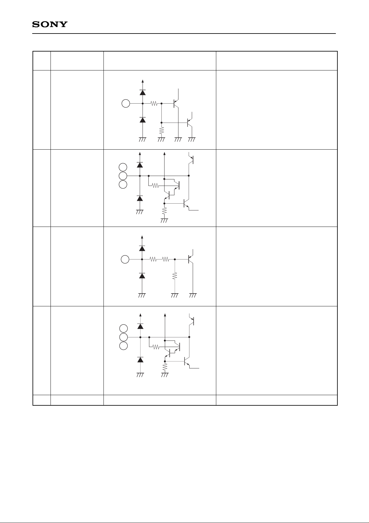
21
IK IN
CRT beam current (cathold current IK)
input. This current is converted to a voltage
inside the IC. This signal is clamped during
the V blanking interval to avoid adversely
affecting AKB operation for the CRT Ieak
current (max. 100µA). The AKB loop
operates by comparing the reference pulse
portion of this signal with the Internal
reference voltage. The RGB output cutoff
can be varied by the bus CUTOFF. The
beam current is large during the video
interval, so attach a Zener diode of around
4V to this pin to protect the IC.
147 4k
21
38.5k
3k
20
AFC FIL
AFC Iag-lead filter connection.
Connect CR to GND.
1k
20
100k
100k
2.5V
Pin
No.
Symbol Equivalent circuit Description
22
23
24
R OUT
G OUT
B OUT
R, G and B signal outputs. 2.4Vp-p is
outputted during 100% white input.
PICTURE: 1Fh
DRIVE: 1Fh
BRIGHT: 1Fh
527
22
23
24
150
1k
12k
19
HD
H drive signal output of NPN transistor.
Open collector output.
147
40k
40k
19
– 9 –
CXA2061S
YS1 switch control.
Selects the RGB1 input.
YS1 Vth: 0.7V
This pin is also used to switch the slave
address. When this pin is 7V or more, the
slave address changes from 88H to 8AH.
SLAVE ADDRESS Vth: 7V
25
YS1
26
27
28
B1 IN
G1 IN
R1 IN
R1, G1 and B1 signal input. Input a 0.7Vp-p
(no sync, 100 IRE) signal via a 0.01µF
capacitor. The input signal is clamped at
the burst timing in SCP.
29
YS2/YM
YS2/YM switch control. Select the RGB2
input. As YM function, when YM is high
(YM Vth: 0.7V), the output signal is
attenuated by 10dB.
YS2 Vth: 2V
147
25
30k
1.2k
60k
26
27
28
29
147 13k
7k
30
31
32
B2 IN
G2 IN
R2 IN
R2, G2 and B2 signal input. Input a 0.7Vp-p
(no sync, 100 IRE) signal via a 0.01µF
capacitor. Same as RGB1 IN, the input
signal is clamped at the burst timing in SCP.
When setting the bus YUV OUT = 1 and
connecting 10kΩ resistors to Vcc, Internal
YUV signals outputs
30 Pin: B-Y output
31 Pin: R-Y output
32 Pin: Y output
30
32
1.2k
60k
31
33
Vcc1
Power supply
Pin
No.
Symbol Equivalent circuit Description

– 10 –
CXA2061S
37
EY IN
1.5k
40k
37
38
39
ER-Y IN
EB-Y IN
External Y, R-Y and B-Y signal inputs.
Input the signal via a 0.01µF capacitor.
EY IN: 0.7Vp-p (no sync)
ER-Y IN: 0.735Vp-p (75% Color Bar)
EB-Y IN: 0.931Vp-p (75% Color Bar)
1.5k
65k
39
38
36
YUV SW
YUV SW control.
Selects the external YUV input.
Vth: 0.7V
This switch has a function prohibited
forcibly only the external Y input by the
register Y SEL.
36
147
20k
I2C Bus protocol SDA (Serial Data) I/O.
35
SDA
35
4k
10k
Pin
No.
Symbol Equivalent circuit Description
34
SCL I2C Bus protocol SCL (Serial Clock) input.
34
4k
10k
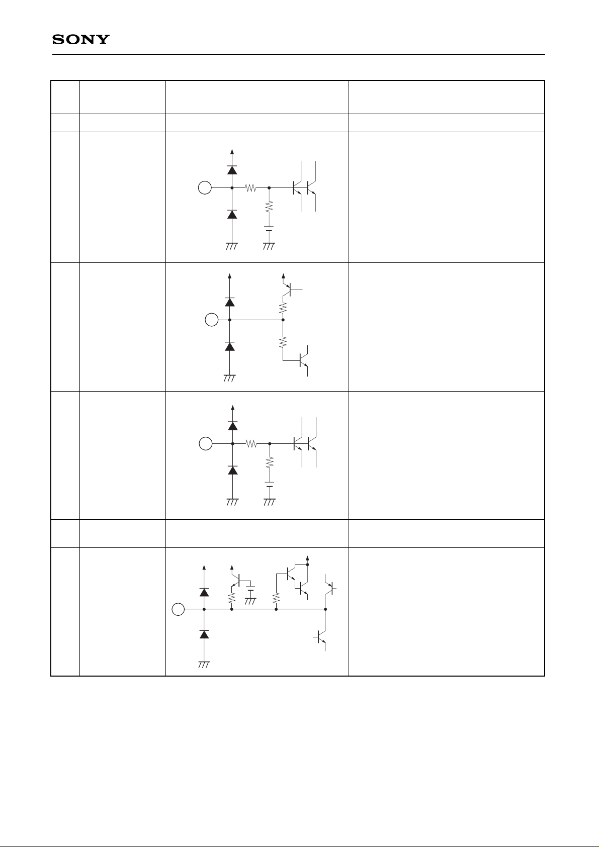
– 11 –
CXA2061S
40 GND2 GND (for the signal block circuit).
CVBS signal input from the TV tuner or
chroma signal input.
Input a 1Vp-p (including sync) CVBS signal
or a chroma signal with a burst level of
300mVp-p via a 1µF capacitor.
Pin
No.
Symbol Equivalent circuit Description
41
CVBS2/Y2 IN
CVBS signal/luminance signal input.
Input a 1Vp-p (including sync) signal via a
1µF capacitor. When inputting Y/C
separated signals, input the Y signal.
42
ABL FIL
Connect a capacitor (4.7µF) to GND to form
the LPF of the ABL control signal.
43
TV/C2 IN
50k
147
5.4V
41
1.2k
42
20k
50k
147
5.4V
43
45
APC FIL
Chroma APC lag-lead filter connection.
Connect CR to GND.
1k
45
4.9V
1k
44 Vcc2
Power supply
(mainly for the chroma block circuit).

– 12 –
CXA2061S
Pin
No.
Symbol Equivalent circuit Description
47
X'tal
APC crystal connection.
X'tal: NTSC crystal (3.579545MHz)
48
NC
2.5k
1.333k
47
46
FSC OUT
FSC output.
Output FSC signal by the register FSC SW.
15k
200
16k
46

– 13 –
CXA2061S
Electrical Characteristics Measurement Condition
Measure the following after setting the I
2
C bus registers as shown in "I
2
C BUS register initial settings". Ta = 25°C, VCC1, VCC2 = 9V, GND1, DND2 = 0V
1
2
3
4
5
6
7
8
9
10
11
I
CC
VREG
fHFR
HDw
VSp-p
VSdc
VEWp-p
VEWdc
VRout1
Vvm
Gmon
Measure the pin inflow current.
Measurement the pin voltage.
H DRIVE output frequency
Measurement the pulse width for the
interval where the H DRIVE output is high.
Measurement the V DRIVE output Vp-p.
Video center bias
Measurement the EW DRIVE output Vp-p.
Video center bias
Output amplitude when a video signal with
an amplitude of 0.7Vp-p/100 IRE is input.
Output amplitude of the 3.58MHz, 0.7Vp-p
input.
Gain from the VIDEO SW input to
MON OUT
V
CC1, VCC2 = 9V
Bus data: Initial setting
H OSC = 7h
ASPECT = 3Fh
V SIZE = 1Fh
SCROLL = 1Fh
V POSITION = 1Fh
ASPECT = 3Fh
V SIZE = 1Fh
PIN AMP = 1Fh
H SIZE = 1Fh
PICTURE = 3Fh
DRIVE = 3Fh
TRAP OFF
Current consumption
REG voltage
Horizontal freerunning frequency
HD output pulse width
V DRIVE output amplitude
V DRIVE output center
potential
EW DRIVE output amplitude
EW DRIVE output center
R, G and B output amplitude
VM output
MON OUT
33, 44
16
19
19
13, 14
13, 14
11
11
22, 23, 24
15
6
mA
V
kHz
µs
V
V
V
V
V
V
dB
No. Item Symbol Measurement condition Measurement point Measurement contents Min. Typ. Max. Unit
Sync deflection block items
75
7.6
15.7
25.5
1.4
3.53
0.73
4
3
2
6
110
7.9
16.0
28
1.6
3.8
0.9
4.3
3.75
2.4
6.4
Signal block items
45
7.4
15.4
23
1.1
3.3
0.4
3.7
2.4
1.6
5.6

– 14 –
CXA2061S
Electrical Characteristic Measurement Circuit
Signal souces are all GND unless otherwise specified in Measurement conditions column of Electrical Characteristics.
YS 1
100
0.01µ
0.01µ
0.01µ
RGB 1 IN
YS 2/YM
100
0.01µ
0.01µ
0.01µ
RGB 2 IN
0.1µ 47µ
100
V
CC + 9V
SCL
100
SDA
100
YUV SW
0.01µ
0.01µ
0.01µ
EXT YUV IN
CVBS2/Y2 IN
1µ
4.7µ
TV/C2 IN
1µ
0.1µ 47µ
10k
0.47µ
470p
NTSC X'tal
18p
25
26
27
28
29
30
40
39
38
37
36
35
34
31
32
33
41
42
43
44
45
46
47
48
APED
C1 IN
ABL IN
CVBS1/Y1 IN
V TIM
MON OUT
COMB-C IN
Y CLAMP
COMB-Y IN
GND1
EW
I REF
VD+
VD–
VM OUT/V PROT
REG
SCP
HP/PROTECT
HD
AFC FIL
IK IN
R OUT
G OUT
B OUT
NC
X'tal
FSCOUT
APC FIL
V
CC2
TV/C2 IN
ABL FIL
CVBS2/Y2 IN
GND2
EB-Y IN
ER-Y IN
EY IN
YUV SW
SDA
SCL
V
CC1
R2 IN
G2 IN
B2 IN
YS2/YM
R1 IN
G1 IN
B1 IN
YS1
4.7µ
0.1µ
9V
1µ
100
1µ
1µ
100
10k
100
51k
100
10µ
1µ
1µ 4.7k
0.01µ
Quasi
CRT
2.2k
51k
H PROT
HP GEN
HD
HP
7µs delay
2
3
4
5
6
7
8
9
10
11
12
13
14
15
16
17
18
19
20
21
22
23
24
1
C1 IN
ABL IN
CVBS1/Y1 IN
V TIM OUT
MON OUT
COMB-C IN
COMB-Y IN
E/W
V PROT
VM OUT
VD OUT
SCP OUT
1k
 Loading...