

Sony CXA2060BS Datasheet

Y/C/RGB/D for PAL/NTSC/SECAM Color TVs
Description
The CXA2060BS is a bipolar IC which integrates
the luminance signal processing, chroma signal
processing, RGB signal processing, and sync and
deflection signal processing functions for PAL/
NTSC/SECAM system color TVs onto a single chip.
This IC includes deflection processing functions for
wide-screen TVs. With a SECAM decoder and 1H
delay line built in for PAL/SECAM, this IC can be
used in configuring multi-color system TV set.
Features
• Supports the I2C bus
• 1H delay line and SECAM decoder
• Supports NTSC/PAL-N/PAL-M systems with three crystal pins
• Deflection compensation circuit for support of various wide modes
• Count down system eliminates need for V oscillation frequency adjustment
• Automatic identification of 50/60Hz vertical frequency (forced control possible)
• Supports non-interlace display (even/odd selectable)
• Automatic identification of PAL, NTSC and SECAM color systems (forced control possible)
• Automatic identification of 4.43MHz/3.58MHz for crystal (forced control possible)
• No adjustment of Y/C filter required
• Three CV inputs, two Y/C inputs (Y/C input shared with CV input), one Y/C input supporting external comb
filter, two RGB inputs
• Dynamic picture/dynamic color circuit
• AKB and gamma correction circuits
• YS1 can be forcibly turned OFF
• FSC output (shared with PAL-N crystal pin)
Applications
Color TVs (4:3, 16:9)
Structure
Bipolar silicon monolithic IC
Absolute Maximum Ratings (Ta = 25°C, GND1, 2 = 0V)
• Supply voltage VCC1, 2 –0.3 to +12 V
• Operating temperature Topr –20 to +75 °C
• Storage temperature Tstg –65 to +150 °C
• Allowable power dissipation PD 1.5 W
(When mounted on a 50mm × 50mm board)
• Voltage at each pin –0.3 to VCC1, 2 + 0.3 V
Operating Conditions
Supply voltage VCC1, 2 9 ± 0.5 V
– 1 –
E98631-PS
Sony reserves the right to change products and specifications without prior notice. This information does not convey any license by
any implication or otherwise under any patents or other right. Application circuits shown, if any, are typical examples illustrating the
operation of the devices. Sony cannot assume responsibility for any problems arising out of the use of these circuits.
CXA2060BS
48 pin SDIP (Plastic)
– 2 –
CXA2060BS
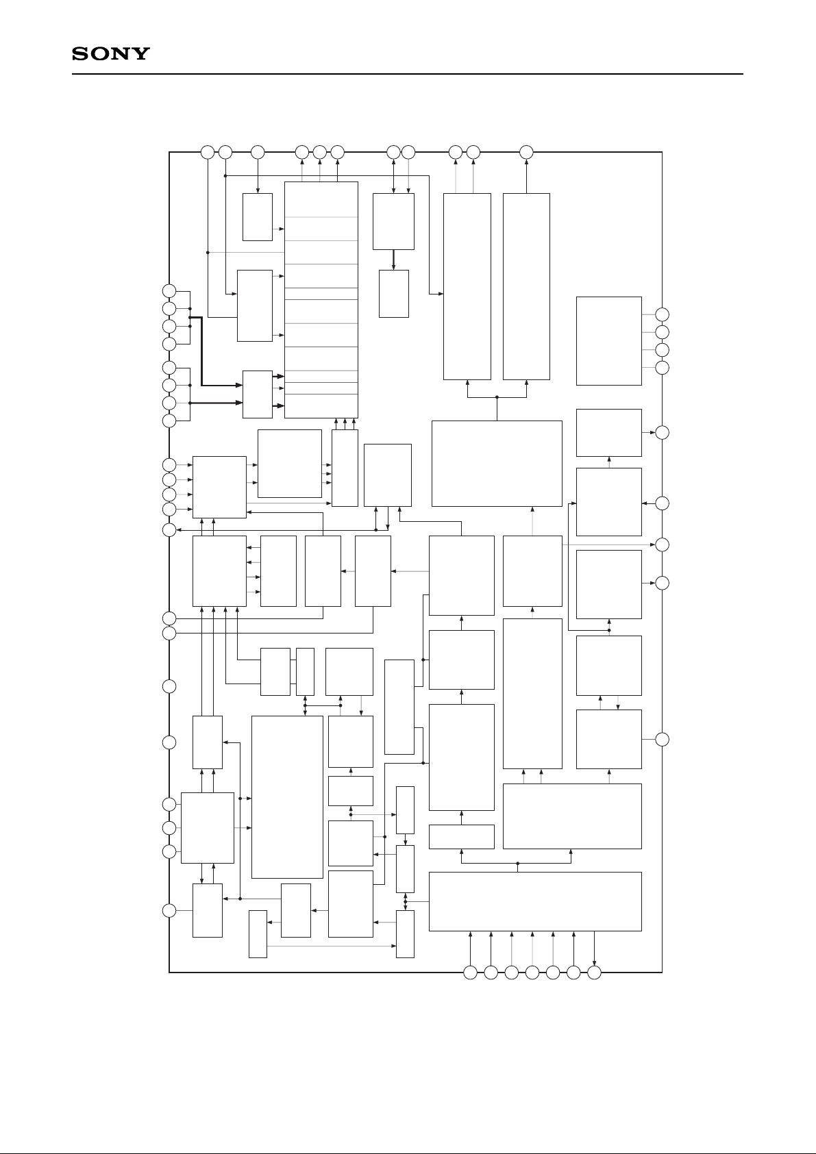
Block Diagram
COLOR AMP
<COLOR>
<C OFF>
AXIS
<AXIS PAL>
<AXIS NTSC>
5
10
11
12
13
14
15
16
17
18
19
21
22
23
24
30
35
34
31
33
1
IK IN
B OUT
G OUT
R OUT
SDA
SCL
VD–
VD+
EW
TV/C2 IN
C1 IN
CVBS2/Y2 IN
CVBS1/Y1 IN
COMB C IN
COMB Y IN
MON OUT
APED
VM OUT/V PROT
EB-Y IN
ER-Y IN
EY IN
YUV SW
R1 IN
G1 IN
B1 IN
YS1
R2 IN (YOUT)
G2 IN (R-YOUT)
B2 IN (B-YOUT)
YS2/YM
SCP
V TIM
HP/PROTECT
V
CC
1
GND1
I REF
REG
HD
<XTAL>
<COL SYSTEM>
<COL LOOP>
<NO COLOR>
<ID STOP>
<ID START>
APC
<HUE>
C VCO
4.433619MHz
3.579545MHz
3.575611MHz
3.582056MHz
PAL/NTSC
DEMOD.
ACC DET.
CHROMA
AMP
ACC DET.ACC AMP
BPF
PAL: 4.43MHz
NTSC: 3.58MHz
<C BPF>
BELL
FILTER
<BELL F0>
LIM
AMP
PLL
SECAM
FM DEMOD.
DE-
EMPHASIS
LINE BLK
SECAM
VCO
CAL. by
4.43MHz
8
40
44
45
APC FIL
V
CC
2
GND2
Y CLAMP
46
47
48
X'TAL 1
X'TAL 2
X'TAL 3
SW
NTSC/
PAL, SECAM
KILLER
<KILLER OFF>
SECAM
PAL/NTSC
FILTER ALIGNMENT
CAL. by fsc
ACC AMP
CHROMA
ATT
TRAP
PAL: 4.43MHz
NTSC: 3.58MHz
SECAM: 4.2 + 4.43MHz
<TRAP OFF>
DL
PAL/NTSC SECAM
<Y DELAY>
SHARPNESS DL
SHARPNESS AMP
<SHARPNESS>
<SHP F0>
<PRE/OVER>
1H
DELAYLINE
(PAL/SECAM)
DPIC
<DPIC>
<AGING>
CLAMP
DC TRAN
<DC TRAN>
CHROMA SW
Y SW
MONITOR SW
VIDEO SW
2
4
6
7
9
41
43
<VIDEO SEL>
<S SEL>
COUNT DOWN
<FIELD FREQ>
<CD MODE>
<INTERLACE>
V SYNC SEP
<VSS>
H SYNC SEP
<HSS>
<HMASK>
<<RFLEVEL>>
LINE COUNTER
V TIM GEN.
<V UNDER SCAN>
<<FIELD ID>>
VSAW GEN.
(50/60)
VTIM
AFC
<AFC GAIN>
<FH HIGH>
<<HLOCK>>
<<HCENT>>
Y
HSAW GEN.
<HOSC>
H TIM GEN.
<H BLK>
<LEFT HBLK>
<RIGHT HBLK>
20
AFC FIL
PHASE DET.
<H POSITION>
<AFC BOW>
<AFC ANGLE>
HPROT
<<HNG>>
HD GEN.
<HD W>
EYUV CLAMP
YUV SW
<Y SEL>
YUV OUT
<YUV OUT>
39
38
37
36
Y/C MIX
RGB CLAMP
VPROT
<<VNG>>
VM AMP
(OFF YS/YM)
DYNAMIC COLOR
<DYNAMIC C>
YS1 SW
<RGB SEL>
YM SW
YS2 SW
PICTURE AMP
<PICTURE>
GAMMA AMP
<GAMMA>
BRIGHT CONT.
<BRIGHT>
DRIVE AMP
<R/G/B DRIVE>
CLAMP
CUTOFF CONT.
<R/G/B CUTOFF>
R/G/B BLK
<PON>
<R/G/B ON>
CLAMP
RGB 1/2
ABL/PEAK LIM
<ABL MODE>
<ABL VTH>
AKB
<<IKR>>
3
42
ABL FIL
ABL IN
26
29
32
I
2
C BUS
DECODER
STATUS I/F
DAC
SW
VD SAW FUNC.
<VON>
<V SIZE>
<V POSITION>
<S CORRECTION>
<V LINEARITY>
<EHT COMP>
EW PARABOLA FUNC.
<H SIZE>
<PIN AMP>
<CORNERPIN>
<TRAPEZIUM>
<EW DC>
WIDE SAW FUNC.
<ASPECT>
<SCROLL>
<UPPER VLIN>
<LOWER VLIN>
<V ZOOM>
<V UNDER SCAN>
IREF REG
27
COLOR SYSTEM DISCRIMINATOR
<ID LEVEL>
<<APC LOCK>>
<<PAL>>
<<SECAM>>
<<XTAL ID>>
25
28
– 3 –
CXA2060BS
Pin Configuration
C1 IN
ABL IN
CVBS1/Y1 IN
V TIM
MON OUT
COMB C IN
COMB Y IN
APED
Y CLAMP
GND1
EW
I REF
VD–
VD+
VM OUT/V PROT
REG
SCP
HD
HP/PROTECT
AFC FIL
IK IN
G OUT
R OUT
B OUT
X'TAL 2
X'TAL 3
X'TAL 1
Vcc2
TV/C2 IN
APC FIL
CVBS2/Y2 IN
GND2
ABL FIL
EB-Y IN
EY IN
YUV SW
ER-Y IN
SCL
Vcc1
SDA
R2 IN
B2 IN
YS2/YM
G2 IN
R1 IN
B1 IN
G1 IN
YS1
1
4
5
6
7
8
9
10
2
3
11
12
13
14
15
16
17
18
19
20
21
22
23
24
25
26
27
28
29
30
31
32
33
34
35
36
37
38
39
40
41
42
43
44
45
46
47
48

– 4 –
CXA2060BS
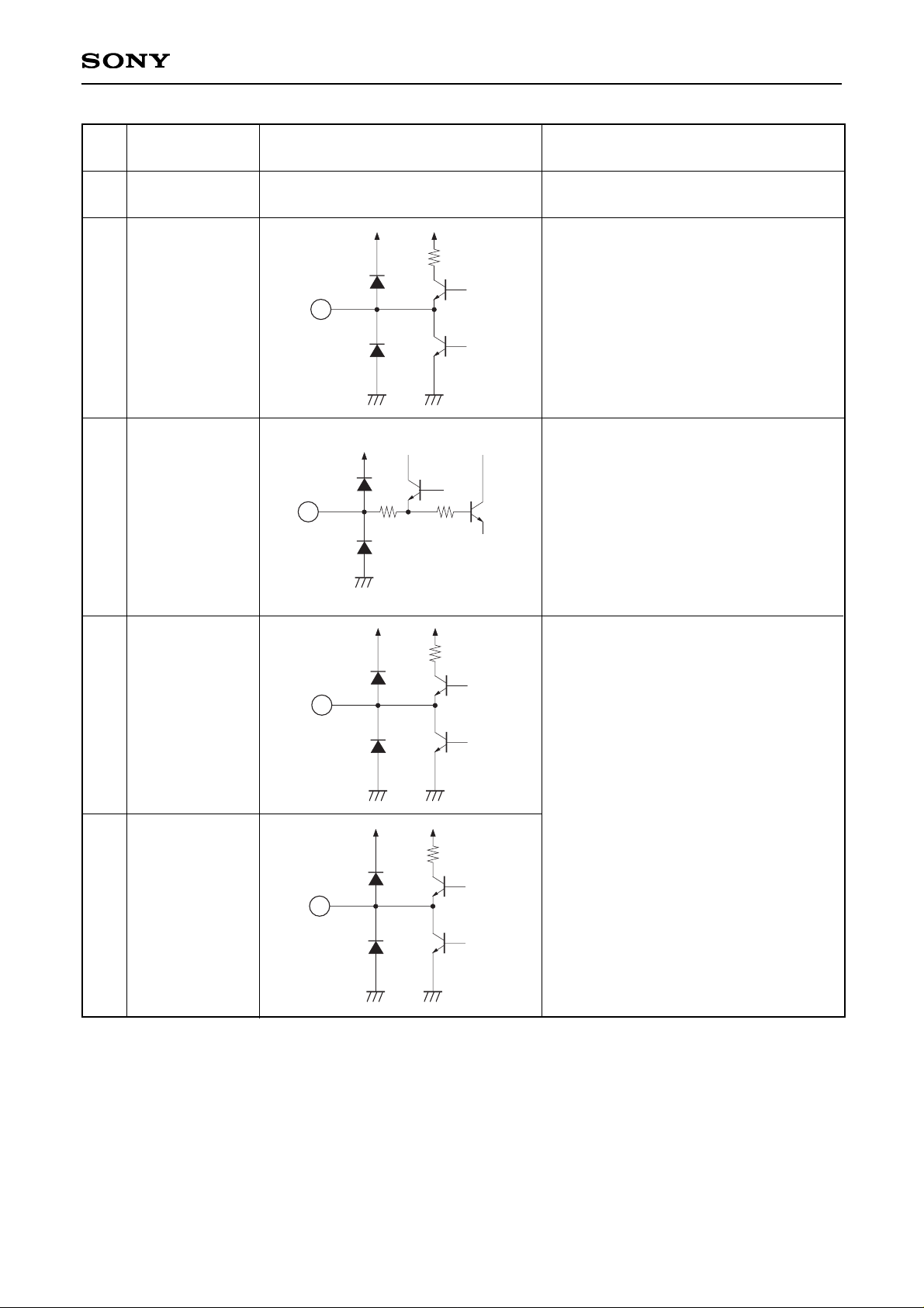
Pin Description
Chroma signal input.
Input a chroma signal having a burst level
of 300mVp-p via a 0.01µF capacitor.
Normally the S pin signal is input.
Pin
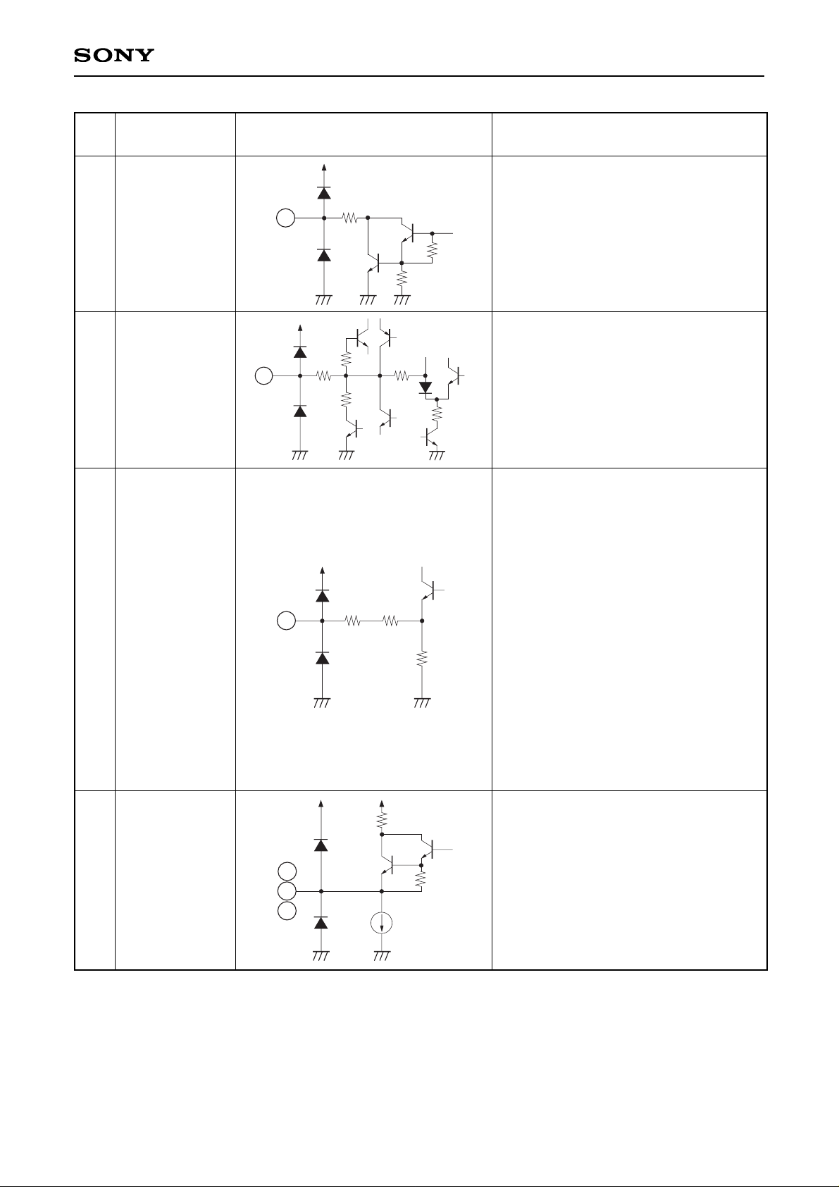
No.
Symbol Equivalent circuit Description
1
APED
Connects a capacitor for black peak hold
of the dynamic picture feature (black
extension).
The 4.7µF capacitor is connected to GND.
2
C1 IN
3
ABL IN
This pin is for both ABL control signal
input and VD high-voltage correction
signal input.
High-voltage correction has linear control
characteristics when this pin's voltage is in
the approximate range of 1V and 8V.
Control characteristics can be varied
using the EHT_COMP control of the bus.
ABL functions as a PIC/BRT-ABL
(average value type).
The threshold voltage at which ABL
activates can be switched to either 3V or
1V depending on the bus.
4
CVBS1/Y1 IN
CVBS signal/luminance signal input.
Input a 1Vp-p (100% white including sync)
CVBS signal via a 1µF capacitor.
Input the Y signal when a separated Y/C
signal is input.
1
94k
1k
1.93k
7.8k
8k
50k
147
5.4V
2
147
130k
3
86k
50k
147
5.4V
4

– 5 –
CXA2060BS
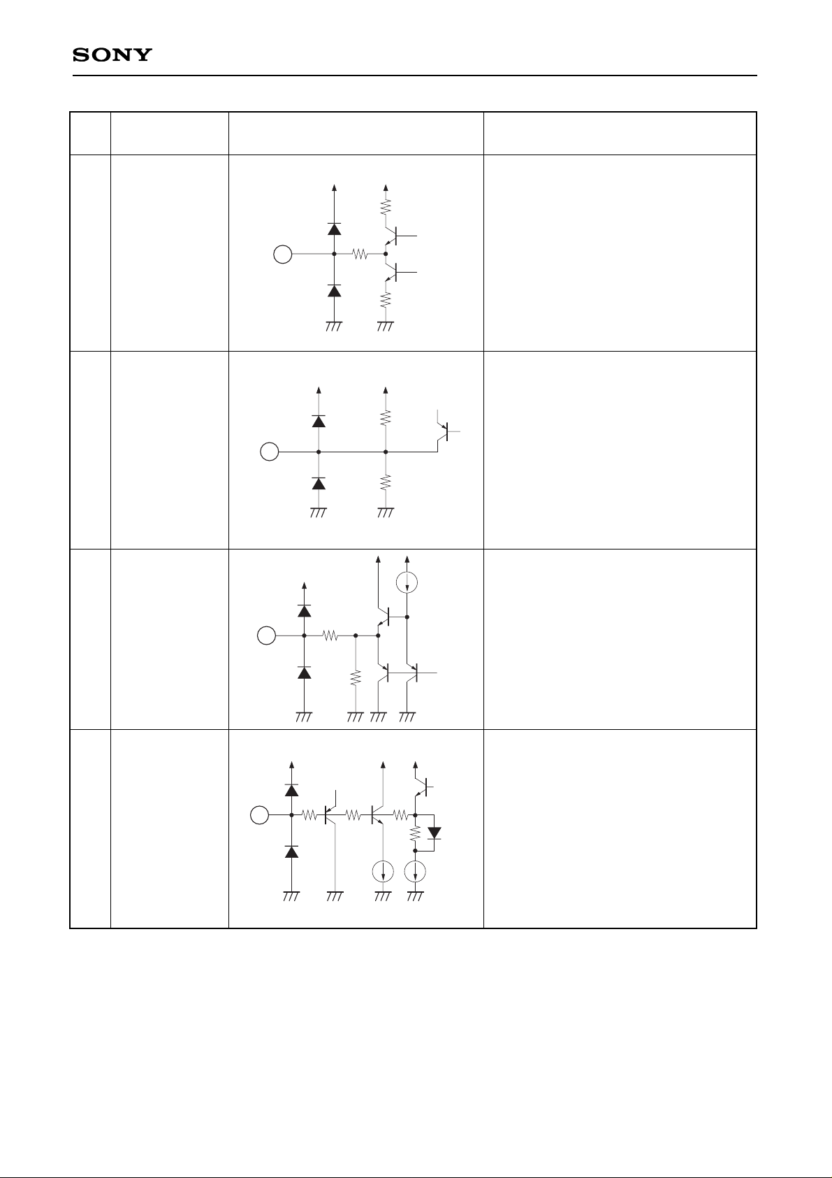
Chroma signal input from a comb filter.
The input chroma signal is a 0.6Vp-p burst
signal.
Pin
No.
Symbol Equivalent circuit Description
6
MON OUT
Output of the signal input from TV, CVBS1
or CVBS2 as selected by VIDEO SEL and
S SEL of the bus.
In the case of S pin input, a luminance
signal and chroma signal are mixed and
output.
Output level is 2Vp-p including sync.
7
COMB C IN
8
Y CLAMP
Connects a capacitor for luminance signal
clamp.
The 0.1µF capacitor is connected to GND.
9
COMB Y IN
Luminance signal input from a comb filter.
The signal is input via a 1µF capacitor
and has a level of 2Vp-p. (100% white
including sync)
147
100µA
100µA
6
25k
147
5.4V
25k
7
10p
1.5k
8
4k
4k
25k
147
5.4V
25k
9
5
V TIM
V timing pulse output.
This is a 0/5V negative polarity pulse.
HSS/VSS can be monitored using the
V TIM SEL register.
147
5
25k
100µA
– 6 –
CXA2060BS
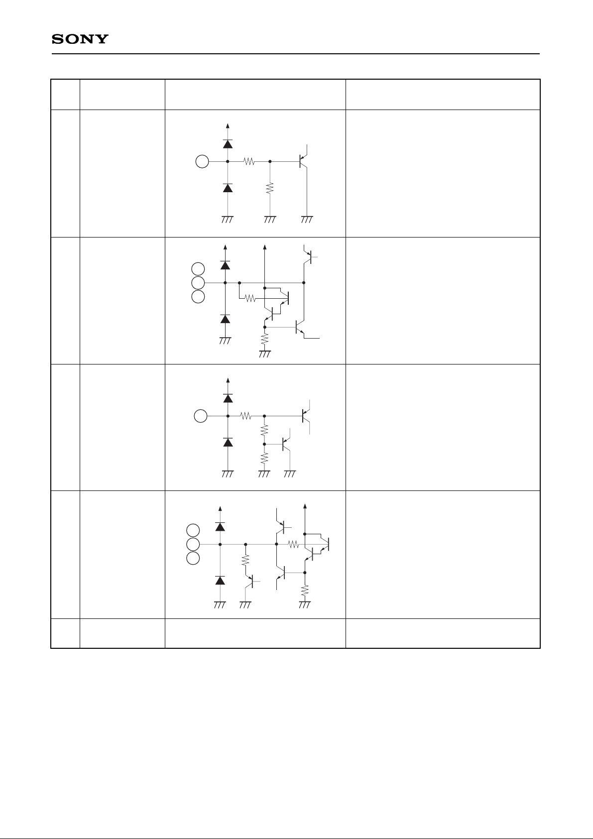
Pin
No.
Symbol Equivalent circuit Description
12
I REF
This pin is used to set the reference
current within the IC.
A 10kΩ resistor (metallic film resistor)
having an error less than 1% is connected
to GND.
13
VD+
14
VD–
V sawtooth wave output.
The polarity of Pin 13 output and Pin 14
output are reversed.
147
7.2k
12
2k
13
2k
14
11
EW V parabola wave output.
1.2k
11
10 GND1
GND for 1HDL and deflection system
circuit.
– 7 –
CXA2060BS
15
VM OUT/
V PROT
Output of luminance signal differential
waveform for VM (Velocity Modulation).
The phase of VM output is synchronized
to the phase of RGB output.
It is approximately 250ns ahead of RGB
output.
This pin is also used for V protect signal
input. When the large current (4mA) is
forcibly drawn through this pin, all RGB
output is blanked, and 1 is output to the
status register VNG.
1k
147
15
1k
16
REG
Decoupling capacitance for the regulator
within the IC.
The 47µF capacitor is connected to GND.
4.4k
500
16
H deflection pulse input for H AFC.
The 5Vp-p pulse is input via a capacitor.
Since this pin is also used to input an XRAY protect signal, a hold down function
activates if this pin's voltage goes above a
"7V cycle" and below 1V. If this occurs,
HD output goes high impedance, RGB
output is blanked, and 1 is output to the
status register HNG. It is necessary to
turn the IC's power OFF then ON again to
cancel this status.
Pin
No.
Symbol Equivalent circuit Description
17
SCP
Sand castle pulse output.
The sand castle pulse is a waveform
superimposed with the burst gate pulse on
the composite blanking pulse.
18
HP/PROTECT
25k
50µA
17
147
147
18
96k
10k 60k
50µA 100µA
– 8 –
CXA2060BS
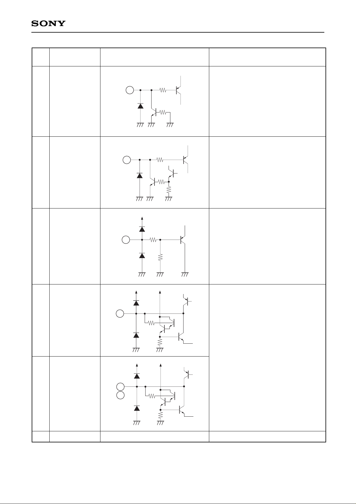
Pin
No.
Symbol Equivalent circuit Description
22
23
24
R OUT
G OUT
B OUT
RGB signal output.
Outputs 3.0Vp-p during 100% white input.
PICTURE: 3Fh
DRIVE: 3Fh
BRIGHT: 1Fh
2mA
12k
200
22
23
24
21
IK IN
CRT beam current input (cathode current
IK).
This current is converted into voltage
within the IC.
In order to eliminate any adverse effects
exercised by CRT leak current (max.
100µA) for AKB operation, it is clamped at
the V blanking interval. The AKB loop is
activated by comparing the reference
pulse component of this signal to the
reference voltage within the IC.
The RGB output cutoff can be varied using
CUTOFF of the bus. The IK reference
signal current can be controlled ±50%
around a 13µA center. Since the beam
current of the video section is large, be
sure to attach a zener diode of about 4V to
the pin to protect the IC.
147
21
3k
4k
19
HD
H drive signal output.
This is open collector output for the NPN
transistor.
20
AFC FIL
Connects an AFC lag lead filter.
CR is connected to GND.
147
20k
20k
19
147
100k
20
30k
1k
100k
– 9 –
CXA2060BS
YS1 switch control pin.
Selects RGB1 input.
YS1 Vth: 0.7V
This pin is also used as the slave address
modification switch.
If the voltage at this pin goes over 7V, the
slave address is changed from 88h to
8Ah.
SLAVE ADDRESS Vth: 7V
25
YS1
26
27
28
B1 IN
G1 IN
R1 IN
RGB1 signal input.
A 0.7Vp-p (no-sync 100 IRE) signal is
input via a 0.01µF capacitor.
The input signal is clamped at the SCP
burst timing.
29
YS2/YM
YS2/YM switch control pin.
Selects RGB2 input.
When operating at High level (YM Vth:
0.7V) as a YM switch the output signal
undergoes 10dB attenuation.
YS2 Vth: 2V
25
147
30k
1.2k
60k
26
27
28
29
147
7k
13k
30
31
32
B2 IN
G2 IN
R2 IN
RGB2 signal input.
A 0.7Vp-p (no-sync 100 IRE) signal is
input via a 0.01µF capacitor. The input
signal is clamped at the SCP burst timing
just as RGB1 IN.
This pin becomes the YUV output pin
based on the YUV OUT register.
Be sure to pull up this pin by 10kΩ when
used for YUV output.
30
32
1.2k
60k
31
100
33 Vcc1
Power pin for the signal block and
deflection block.
Pin
No.
Symbol Equivalent circuit Description
– 10 –
CXA2060BS
I2C bus standard SDA (Serial Data)
input/output.
Pin
No.
Symbol Equivalent circuit Description
34
SCL
I2C bus standard SCL (Serial Clock) input.
35
SDA
36
YUV SW
YUV SW control pin.
Selects external YUV input.
Vth: 0.7V
This switch includes a function for forcibly
turning OFF external Y input only using
Y SEL of the bus.
37
EY IN
34
4k
10k
35
4k
7.5k
7.5k
36
147
20k
1.5k
40k
37
38
39
ER-Y IN
EB-Y IN
External Y/R-Y/B-Y signal input.
Input is via a 0.01µF capacitor.
EY IN: 0.7Vp-p (no sync)
ER-Y IN: 0.735Vp-p (75% color bar)
EB-Y IN: 0.931Vp-p (75% color bar)
1.5k
65k
39
38
40
GND2
GND pin for signal block circuits.
– 11 –
CXA2060BS
Input of CVBS signal from a TV tuner or
chroma signal.
A 1Vp-p (including sync) CVBS signal or
300mVp-p burst chroma signal is input
via a 1µF capacitor.
Pin
No.
Symbol Equivalent circuit Description
41
CVBS2/Y2 IN
CVBS signal/luminance signal input.
A 1Vp-p signal (including sync) is input
via a 1µF capacitor.
Input the Y signal when a separated Y/C
signal is input.
42
ABL FIL
Connects the capacitor (4.7µF) forming
the ABL control signal LPF to GND.
43
TV/C2 IN
50k
147
5.4V
41
1.2k
42
20k
200k
50k
147
5.4V
43
45
APC FIL
Connects a chroma APC lag lead filter.
CR is connected to GND.
1k
45
4.6V
1k
44
Vcc2
Power pin for the signal block.

– 12 –
CXA2060BS
46
X'tal 3
Connects an APC crystal.
The crystals should be connected as
follows.
X'tal 3: PAL-N crystal (3.58205625MHz)
X'tal 2: NTSC crystal (3.579545MHz)
X'tal 1: PAL/SECAM crystal
(4.43361875MHz) or
PAL-M crystal
(3.57561149MHz)
Pin 46 can be switched for use as FSC
output using the FSCSW register.
2V DC, 0.7Vp-p signal is output.
2k
1.33k
46
Pin
No.
Symbol Equivalent circuit Description
47
X'tal 2
48
X'tal 1
2k
1.33k
47
48
2k
1.33k
1k
– 13 –
CXA2060BS
Electrical Characteristics Measurement Conditions
Set I
2
C bus registers to I
2
C Bus Register Initial Setting Values and measure them. Ta = 25°C, VCC1, VCC2 = 9V, GND1, GND2 = 0V
1
No.
Item
Current consumption
Symbol
I
CC
Measurement conditions
V
CC1, VCC2 = 9V
Bus data: initial setting values
Measure-
ment pin
33, 44
Measurement contents
Measure the current flowing into the pin.
Min.
Typ.
Max.
Unit
80 125 170
mA
2
Horizontal free-running
frequency
fHFR
HOSC = 7 (no input signal)
FH HIGH = 1
19
18
17
H drive output frequency
15.5
15.7 15.9
kHz
3
Horizontal free-running
frequency 2
fHHIFR
FH HIGH = 0
4 HD pulse width HDw HDW = 0
5 HD pulse width 2 HDw
HDW = 1
tstr (HP) = 7.5µs, tHP = 12µs
6
HP phase HPph HPph = HP (cent) – Hsync (cent)
8
H BLK pulse width
HBLKw
7
H BLK phase
HBLKph
HBLKph = SCP (HBLKrise) –
Hsync (cent)
10
BGP pulse width
BGPw
9
BGP phase
BGPph
BGPph = SCP (BGPrise) –
Hsync (cent)
16.2
16.7
17.2
kHz
22.5 24
25.5
µs
19 20
21
µs
3.0 3.7 4.4
µs
9
10
11
µs
–2.5
–1.75
–1
µs
2.8
3.0
3.2
µs
3.4
3.9
4.4
µs
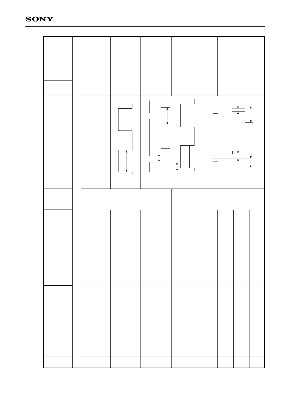
Sync deflection block items
HDW
HD
HDW
12µs
HPph
Hsync
7.5µs
HD
HP
Hsync
SCP
BGPph
HBLKph
HBLKw
BGPw
– 14 –
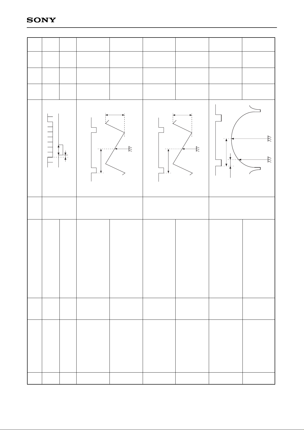
CXA2060BS
5
13
11
11
VTIM phase VTIMph
C/D non-standard mode
VTIMph = VTIM (fall) – Vsync (fall)
12
VTIM pulse width VTIMw
15
V drive output
center voltage
(60Hz)
∆VSdc
60Hz – 50Hz
∆VSdc = VSdc2 – VSdc1
16
V drive output
amplitude
(60Hz)
∆VSp-p
60Hz/50Hz
∆VSp-p = VSp-p2/VSp-p1 × 100
17
EW drive output
center voltage
(50Hz)
VEWdc1
50Hz
18
EW drive output
amplitude
(50Hz)
VEWp-p
50Hz
VEWp-p = VEWdc1 – VEWdc0
10
20
30
µs
45
60
75
µs
–10
0
10
mV
99
100
101
%
3.9
4.1
4.3
V
450 560
670
mV
VTIMph
VTIMw
Vsync
VTIM
8.78ms
VSdc2
VSp-p2
Vsync
VD+
13
13
V drive output
center voltage
(50Hz)
VSdc1
50Hz
14
V drive output
amplitude
(50Hz)
VSp-p1
50Hz
3.4
3.6
3.8
V
1.2
1.35
1.5
V
10.6ms
VSdc1
VSp-p1
Vsync
VD+
Vsync
EW
10.6ms
1.5ms
VEWdc0 VEWdc1
No.
Item
Symbol
Measurement conditions
Measure-
ment pin
Measurement contents Min.
Typ.
Max.
Unit
– 15 –
CXA2060BS
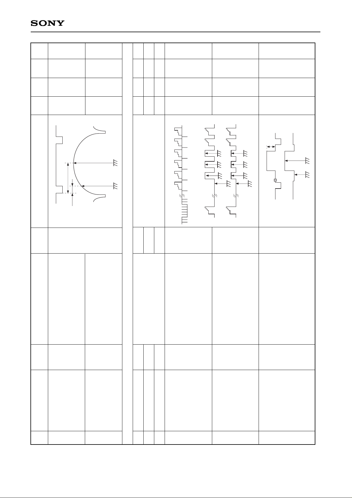
21
21
24
IK current (Max.)
IIK
R CUTOFF = Fh
G CUTOFF = Fh
B CUTOFF = Fh
IIK = (Vrrf – V0)/4k
25
IK current (Min.)
∆IIK
R CUTOFF = 0h
G CUTOFF = 0h
B CUTOFF = 0h
IIKmin/IIKmax
15
22
29
µA
27 32
37
%
11
22
23
24
19
EW DRIVE output
center voltage
(60Hz)
∆VEWdc
60Hz – 50Hz
∆VEWdc = VEWdc2 – VEWdc1
20
EW DRIVE output
amplitude
(60Hz)
∆VEWp-p
60Hz/50Hz
∆VEWp-p = (VEWdc2 – VEWdc20)/
VEWp-p × 100
21
22
23
R BLK voltage
G BLK voltage
B BLK voltage
VRBLK
VGBLK
VBBLK
P ON = 0
–10
0
10
mV
97
100
103
%
0
0.15 0.3 V00.15 0.3 V00.15 0.3 V
Vsync
EW
8.78ms
1.5ms
VEWdc20 VEWdc2
TV/C2IN
IKIN (Max.)
22H 23H 24H 25H 26H 27H
IKIN (Min.)
V0 Vrrf Vgrf Vbrf
V0
Vgrf Vbrf
Vrrf Vgrf Vbrf
32
26
Luminance (Y) output
Vy
YUV OUT = 1
Vy = V1 – V0
610
670
730
mV
0.7V
TV/C2IN
R2IN (YOUT)
V1V0
Measure the pin voltage.
Signal block items
No.
Item
Symbol
Measurement conditions
Measure-
ment pin
Measurement contents Min.
Typ.
Max.
Unit

– 16 –
CXA2060BS
22, 23, 24
28
RGB BRIGHT voltage
Vbrt
Black level – Ref. P. level
Rch: Vbrtr = Vrb – Vrrf
Gch: Vbrtg = Vgb – Vgrf
Bch: Vbrtb = Vbb – Vbrf
–450
–400 –350
mV
22, 23, 24
27
RGB amplitude ratio
∆G
∆G
R = 20 × log ((VR1 – VR0)/Vy)
∆G
G = 20 × log ((VG1 – VG0)/Vy)
∆G
B = 20 × log ((VB1 – VB0)/Vy)
12
13.5
15
dB
0.7V
VR1VR0
TV/C2IN
ROUT
VR1VR0
GOUT
VG1VG0
BOUT
VB1VB0
TV/C2IN
ROUT
22H 23H 24H 25H 26H 27H
GOUT
Vrrf Vrb
Vgrf Vgb
VbbVbrf
BOUT
31
30
29
SECAM color difference
(R-Y) output
Vr-y
SECAM signal (75%)
Vr-y = Vr1 – Vr0
30
SECAM color difference
(B-Y) output
Vb-y
SECAM signal (75%)
Vb-y = Vb1 – Vb0
690
800
910
mV
880
1040
1200
mV
TV/C2IN
G2IN (R-YOUT)
B2IN (B-YOUT)
B-Y
R-Y
BLUE RED
YELLOW CYAN
B-YID R-YID
Vr1 Vr0
Vb1 Vb0
No.
Item
Symbol
Measurement conditions
Measure-
ment pin
Measurement contents Min.
Typ.
Max.
Unit

– 17 –
CXA2060BS
31
30
31
PAL color difference
(R-Y) output
Vr-y
PAL signal
Vr-y = Vr1 – Vr0
32
PAL color difference
(B-Y) output
Vb-y
PAL signal
Vb-y = Vb1 – Vb0
900
1000
1100
mV
430
500
570
mV
Vr1Vr0
700mVp-p
±90deg
400mVp-p
0deg
G2IN (R-YOUT)
B2IN (B-YOUT)
Vb1Vb0
TV/C2IN
30, 31
33
HUE center offset
φoffset
YUV OUT = 1, NTSC signal
φoffset = tan
–1
(4/7 × ((Vb1 – Vb0)/
(Vb2 – Vb0)))
–6
0
6
Deg
Vb0 Vb1Vb2
B2IN (B-YOUT)
700mVp-p
90deg
400mVp-p
0deg
TV/C2IN
15
34
VM output
Vvm
3.58MHz 700mVp-p
1.8 2.3
2.8
V
700mVp-p
3.58MHz
Vvm
VMOUT/VPROT
TV/C2IN
46
35
FSC output
Vfsc
FSC SW = 1
500 900
1300
mV
Vfsc
FSCOUT
No.
Item
Symbol
Measurement conditions
Measure-
ment pin
Measurement contents Min.
Typ.
Max.
Unit
 Loading...