

Sony CXA2040AQ Datasheet
– 1 –
CXA2040AQ
E96Z28-PS
I2C Bus-Compatible Video Switch
Description
The CXA2040AQ is an I2C bus-compatible 5-input,
3-output video switch for TVs.
Features
• Serial data control via I2C bus
• 5 composite video input systems
• 2 Y/C (S terminal) input systems
• 3 composite video output systems
• 1 Y/C (S terminal) output system
• Input can be selected independently for each
output system.
• SYNC_ID function for CV1 system input
• Built-in 6dB amplifier for CVOUT2 system output
• Built-in Y/C MIX circuit
• Slave address can be changed (90H/92H).
• High impedance maintained by I2C bus line (SDA,
SCL) even when power is OFF.
Applications
TVs
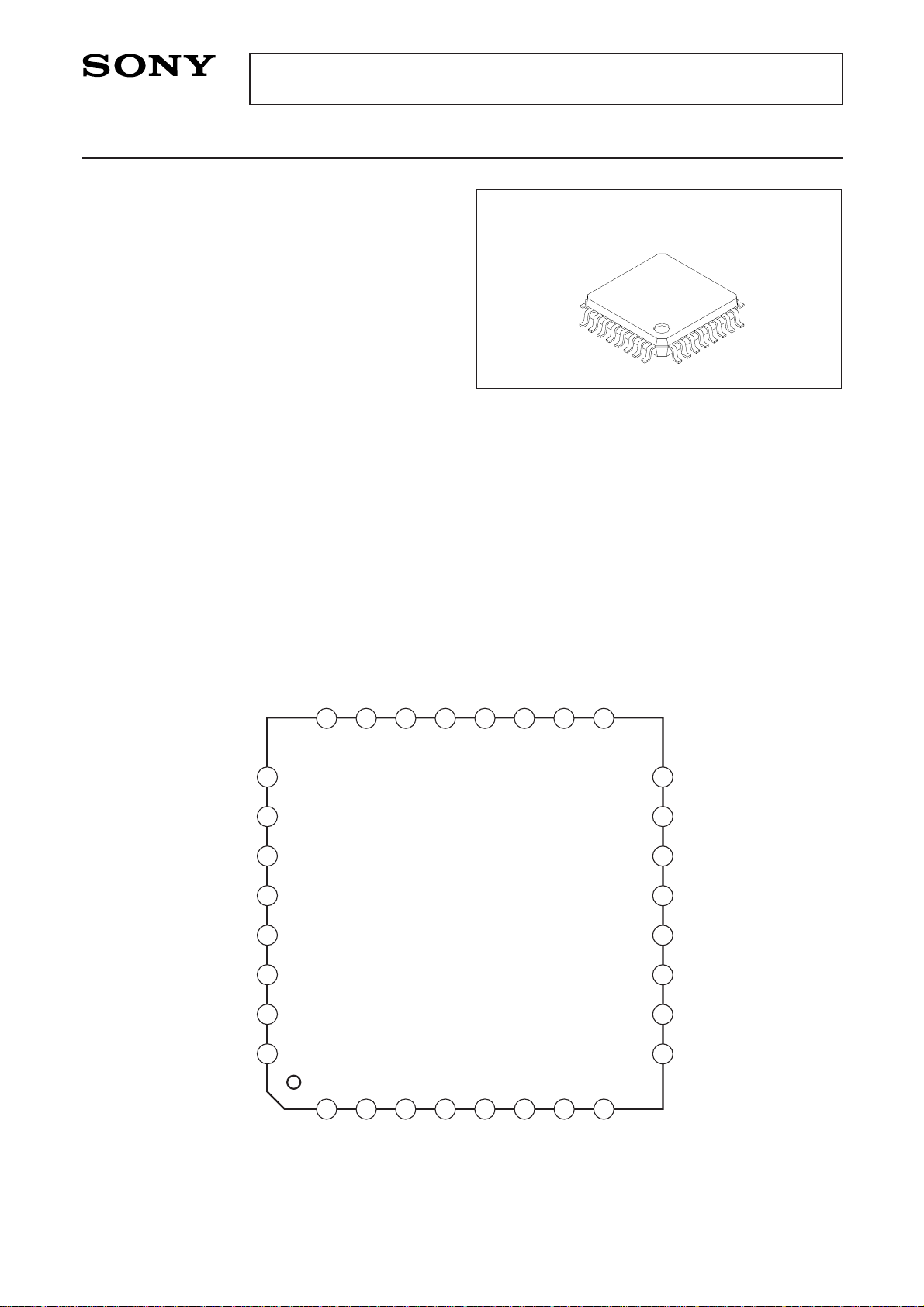
Pin Configuration (Top View)
Absolute Maximum Ratings (Ta = 25°C)
• Supply voltage VCC 12 V
• Operating temperature Topr –20 to +75 °C
• Storage temperature Tstg –65 to +150 °C
• Allowable power dissipation PD 1.0 W
(when mounted on a 50mm × 50mm board)
Operating Conditions
Supply voltage VCC 9.0 ± 0.5 V
Structure
Bipolar silicon monolithic IC
Sony reserves the right to change products and specifications without prior notice. This information does not convey any license by
any implication or otherwise under any patents or other right. Application circuits shown, if any, are typical examples illustrating the
operation of the devices. Sony cannot assume responsibility for any problems arising out of the use of these circuits.
32 pin QFP (Plastic)
NC
CV1
SYNCTC
SDA
SCL
ADR
NC
CVOUT1
17
18
19
20
21
22
23
24
NC
CVOUT2
NC
CVOUT3
NC
YOUT
NC
COUT
9
10
11
12
13
14
15
16
Y1
GND
C1
S1
Y2
S2
C2
NC
2
3
4
5
6
7
8
1
BIAS
CV2
V
CC
CV3
GND
CV4
GND
CV5
26
27
28
29
30
31
32
25
– 2 –
CXA2040AQ
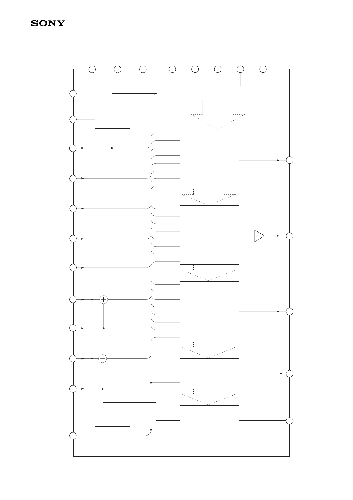
Block Diagram
CVOUT1
CVOUT2
CVOUT3
YOUT
COUT
SW1
SW2
SW3
CV1
CV2
CV4
CV6
MUTE
CV3
CV5
CV7
CV1
CV2
CV4
CV6
MUTE
CV3
CV5
CV7
CV1
CV2
CV4
CV6
MUTE
CV3
CV5
CV7
CV7
CV6
CV5
CV4
CV3
CV2
CV1
MUTE
SYNC DETECT
MUTE
C2
C1
SW5
BIAS
MUTE
Y2
Y1
SW4
CV2
CV3
CV4
CV5
BIAS
SYNCTC
CV1
22
23
32
C2
Y2
C1
Y1
7
17
9
11
13
15
5
3
1
27
29
31
25
6dB
S2
ADR
SCL
SDA
I2C BUS DECODER
6
S1
4
19
20
21
26
V
CC
30
GND
2
GND
28
GND
∗
Numbers inside circles indicate the IC pin numbers.

– 3 –
CXA2040AQ
Pin Description
Pin
No.
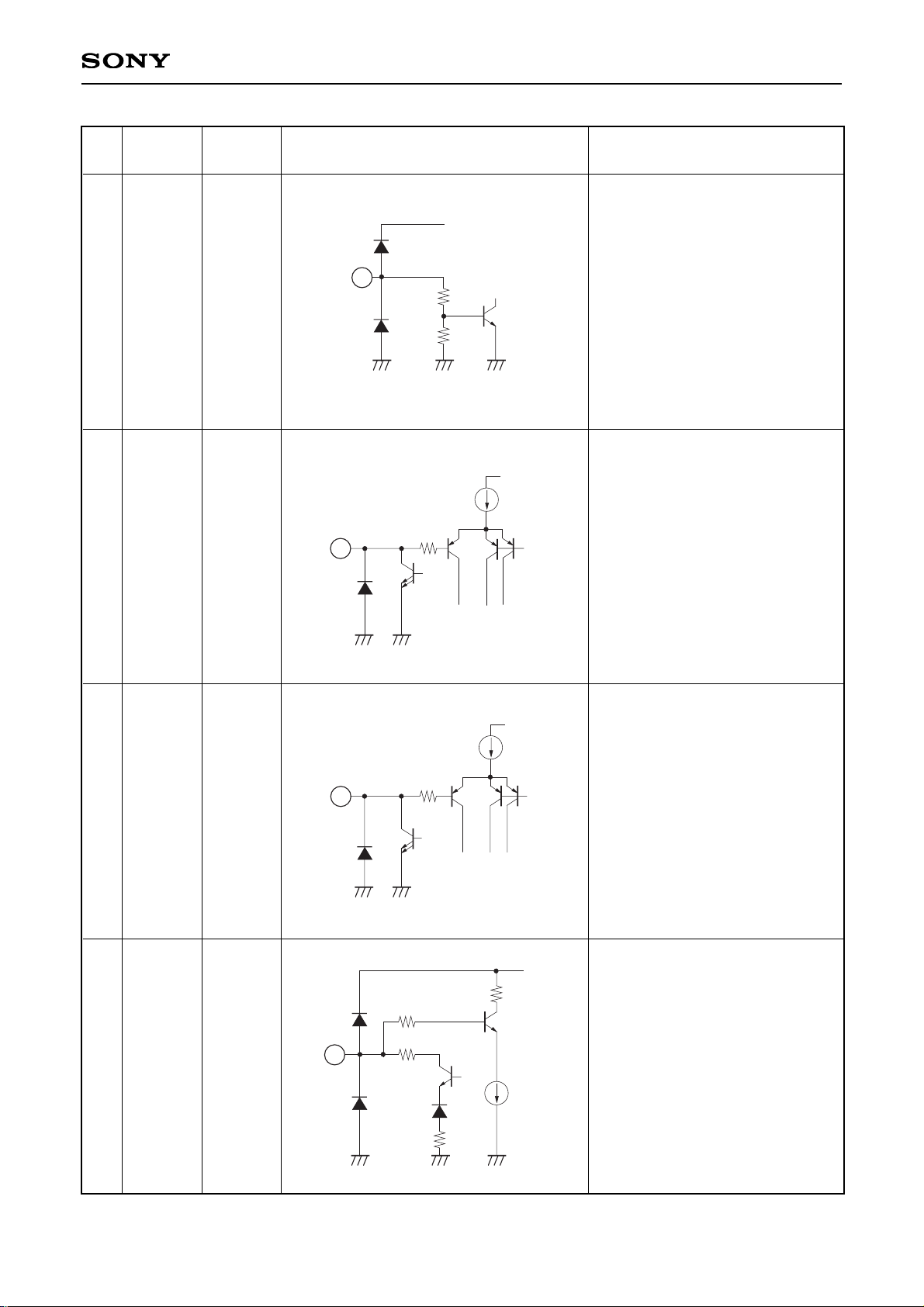
Symbol Pin voltage Equivalent circuit Description
1
5
3
7
Y1
Y2
C1
C2
4.5V
Y/C separation signal inputs.
Biased to approximately 4.5V.
Input the input signals through
capacitors. Connect protective
resistor of 220Ω between these
pins and the capacitors.
Y1 and Y2 pins: Luminance
signals input.
C1 and C2 pins: Chrominance
signals input.
46S1
S2
Applying a DC voltage to S1 and
S2 pins allows these voltages to
be applied to the microcomputer
as the I2C bus status register data.
S1, S2 = 0 to 2V
OPEN = 0, SEL = 1
S1, S2 = 4.75 to 7.25V
OPEN = 0, SEL = 0
S1, S2 = 9.5 to 12V
OPEN = 1, SEL = 0
119YOUT
COUT
4.5V
Y/C signal outputs.
YOUT pin: Luminance signal
output.
COUT pin: Chrominance signal
output.
17
15
13
CVOUT1
CVOUT2
CVOUT3
4.5V
Composite video signal outputs.
CVOUT1, CVOUT2:
0dB output with respect to
the input signal.
CVOUT2:
+6dB output with respect
to the input signal.
5
7
1
20k
147
28k
V
CC
× 2
3
6
50k
100k
V
CC
50k
4
× 4
VCC
× 2
200 1.2k
× 2
× 5
× 6
9
11
VCC
× 2
200 1.2k
× 2
× 5
× 6
13
15
17
– 4 –
CXA2040AQ
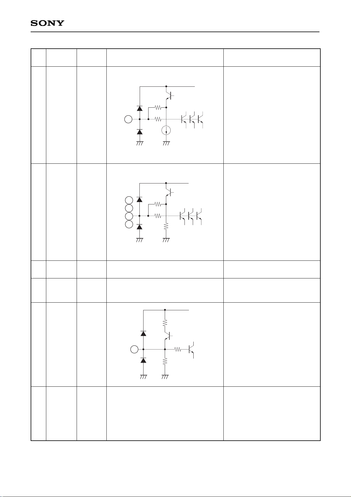
19 ADR
Selects the slave address for the
I2C bus.
90H at 1.0V or less
92H at 3.5V or more
90H when open
20 SCL —
I2C bus signal input.
Connect protective resistor of
220Ω between this pin and the
SCL line.
21 SDA —
I2C bus signal input.
Connect protective resistor of
220Ω between this pin and the
SDA line.
22 SYNCTC
Sync tip clamp time constant for
Sync Separation.
Connect 68kΩ resistor between
this pin and VCC.
Connect 0.1µF capacitor between
this pin and GND.
19
72k
28k
VCC
20
4k
× 4
V
CC
21
4k
× 6
V
CC
1.2k
V
CC
22
147
147
1.2k
Pin
No.
Symbol Pin voltage Equivalent circuit Description
– 5 –
CXA2040AQ
23 CV1 3.1V
Composite video signal input.
Clamped to approximately 3.1V.
Input the input signal through
capacitor. Connect protective
resistor of 220Ω between this pin
and the capacitor.
The composite video signal input
to CV1 is also taken into the
"SYNC DETECT circuit" of which
SYNC is existed or not.
25
27
29
31
CV2
CV3
CV4
CV5
4.5V
Composite video signal input.
Biased to approximately 4.5V.
Input the input signals through
capacitors. Connect protective
resistor of 220Ω between these
pins and the capacitors.
26 VCC
9.0V
∗1
Power supply.
Apply 9.0V.
2
28
30
GND
0.0V
∗1
GND.
32
8
10
12
14
16
18
24
BIAS
NC
4.5V
4.5V bias.
Attach a decoupling capacitor
between this pin and GND.
This pin cannot be used as an
external power supply.
NC (not connected).
Connect to GND.
If these NC pins are not connected
to GND, the cross talk and other
desired values indicated in the
Electrical Characteristics cannot
be obtained.
23
4k
147
V
CC
20k
147
28k
V
CC
25
27
29
31
20k
V
CC
32
22.5k
1.2k
∗1
Applied externally.
Pin
No.
Symbol Pin voltage Equivalent circuit Description

– 6 –
CXA2040AQ
Measure the pin inflow
current.
Measure the pin voltage.
20Log
20Log
20Log
∗
Since the sum of 0.15Vp-p
and 0.15Vp-p is input to
each switch, calculations
are performed with 0.3Vp-p.
No. Item
Symbol
Measurement conditions
V
CC = 9V, no signal
VCC = 9V, no signal
CV1 In, CV2 In, CV3 In,
CV4 In or CV5 In
100kHz, 0.3Vp-p CW
Select each input with I
2
C bus
control and obtain the I/O gain.
CV1 In, CV2 In, CV3 In,
CV4 In or CV5 In
100kHz, 0.3Vp-p CW
Select each input with I
2
C bus
control and obtain the I/O gain.
Y1 and C1 (CV6) In or
Y2 and C2 (CV7) In
100kHz, 0.15Vp-p CW
Select each input with I
2
C bus
control and obtain the I/O gain.
26
32
13, 17
15
13, 17
18.0
4.25
–0.40
5.75
–0.40
28
4.50
0.00
6.25
0.10
39.0
4.75
0.40
6.75
0.60
mA
V
dB
dB
dB
1
2
3
4
5
Current
consumption
Pin voltage
CV system
gain 1
CV system
gain 2
CV system
(Y/C MIX)
gain 1
I
CC
VBIAS
GCV11
GCV21
GCVM11
Measurement pins
Measurement contents Min. Typ. Max. Unit
VCV11
VCV21
VCVM11
VCV11
0.3Vp-p
VCV21
0.3Vp-p
VCVM11
0.3Vp-p
Electrical Characteristics See Electrical Characteristics Measurement Circuit 2 for Cross talk and MUTE. (Ta = 25°C, VCC = 9V)
See Electrical Characteristics Measurement Circuit 1 for all other items.
– 7 –
CXA2040AQ
20Log
∗
Since the sum of 0.15Vp-p
and 0.15Vp-p is input to
each switch, calculations
are performed with 0.3Vp-p.
20Log
20Log
20Log
∗
VCV11 and VCV12 should be
the same I/O.
Y1 and C1 (CV6) In or
Y2 and C2 (CV7) In
100kHz, 0.15Vp-p CW
Select each input with I
2
C bus
control and obtain the I/O gain.
Y1 In or Y2 In
100kHz, 0.3Vp-p CW
Select each input with I
2
C bus
control and obtain the I/O gain.
C1 In or C2 In
100kHz, 0.3Vp-p CW
Select each input with I
2
C bus
control and obtain the I/O gain.
CV1 In, CV2 In, CV3 In,
CV4 In or CV5 In
10MHz, 0.3Vp-p CW
Select each input with I
2
C bus
control and obtain the I/O gain.
Then obtain the difference from the
I/O gain measured by Test 3.
15
11
9
13, 17
5.75
–0.40
–0.40
–0.85
6.40
0.00
0.00
–0.15
7.05
0.40
0.40
0.55
dB
dB
dB
dB
6
7
8
9
CV system
(Y/C MIX)
gain 2
Y system
gain
C system
gain
CV system
frequency
response 1
G
CVM21
GY11
GC11
∆GCV12
VCVM21
VY11
VC11
VCV12
VCVM21
0.3Vp-p
VY11
0.3Vp-p
VC11
0.3Vp-p
VCV12
VCV11
No. Item
Symbol
Measurement conditions
Measurement pins
Measurement contents Min. Typ. Max. Unit
 Loading...