

Sony CXA2038R Datasheet

—1—
E95Y03A77-TE
Sony reserves the right to change products and specifications without prior notice. This information does not convey any license by
any implication or otherwise under any patents or other right. Application circuits shown, if any, are typical examples illustrating the
operation of the devices. Sony cannot assume responsibility for any problems arising out of the use of these circuits.
Absolute Maximum Ratings (Ta=25 °C)
• Supply voltage VCC 7V
•Operating temperature Topr –20 to +75 °C
• Storage temperature Tstg –65 to +150 °C
• Allowable power dissipation
PD 1120 mW
(When mounted on board)
Operating Conditions
• Recommended supply voltage
VCC 3.15 V
VCCH 4.75 V
• Supply voltage range VCC 3 to 5.25 V
VCCH 4.5 to 5.25 V
However, VCCH ≥ VCC
Description
The CXA2038R is a bipolar IC designed as an
AFM monaural signal processor for 8 mm VCRs. All
functions necessary for AFM monaural are
concentrated onto a single 64-pin LQFP.
Features
• Low supply voltage (3.15 V) design
• Low power consumption (VCC=3.15 V)
Recording: 65 mW
Playback: 103 mW
• Built-in BPF (1.5 MHz)
• FM modulator center frequency made non-
adjusting.
• Supports NTSC and PAL
• Enables both parallel and 3-line serial mode
control
• Supports electronic volume (EVR) control
Applications
8 mm VCRs
Structure
Bipolar silicon monolithic IC
AFM Monaural Signal Processor for 8 mm VCR
64 pin LQFP (Plastic)
CXA2038R
—2—
CXA2038R
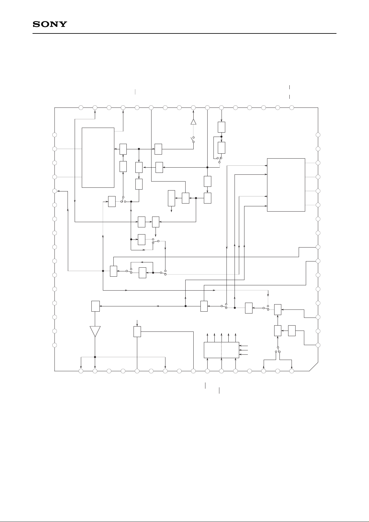
Block Diagram
MIC/LINE (CS)
REC/PB (CK)
(S I)
PMUTETC
MIXOUT
MICIN
VCC1
REC ON
SP
LP
MUTE
PB
REC
VCT5
VCC2
VCCH
AFLIM
PB
REC
PB
REC
PBREC
BPF
ON
OFF
PLLLPF
DEVADJ
S / HTC
MUTE
LPEMPTC
MONITOR
BPMONICT
GND2
VCTH
NC
NC
NC
NC
NC
NC
NC
FADE
GND1
RFDC
IFDC
WEIGHT
TCH
TC
NRDC
ALCDET
VCTTC
IREF
NC
NC
NC
NC
NC
LINEIN
MUTEOUT
LINE
MIC
PLL
ENC IN
ENC OUT
DEC IN
DEC OUT
NR
POWER
MUTE
MUTE
CONTROL
BUS
DECODER
ALC
DET
FADE
LPF
D.C.
BUF
MUTE
D.C.
MUTE
LPEMP
1.5MHz
VCO
LIM
LPF
LIM
LPF
PHASE
COMP
1.5M
BPF
RF
AGC
DOC
DET
FWR
MUTE
DET
MUTE OFF
DELAY
OR
PG
DOUB
S / H
17
18
19
20
21
22
23
24
25
26
27
28
29
30
31
32
33343536373839404142434445464748
49
50
51
52
53
54
55
56
57
58
59
60
61
62
63
64
101 2 3 4 5 6 7 8 9 1514131211 16
LINEOUT
EPOUT
GNDH
NC
PBRFIN
MUTETC
RECFMOUT
RFSWP
FSCIN
BPFMONI
AGC TC
NC
NC
NC
NC
NC
VCT
BPF fo ADJ
NTSC/PAL
SP/LP (SI/PA)

—3—
CXA2038R
Pin Description (VCC1, VCC2=3.15 V, VCCH=4.75 V, Ta=27 °C)
Pin
No.
1
2
3
4
5
Symbol
ALCDET
NC
FADE
NC
NC
Pin voltage
DC AC
— —
— —
See
attached —
sheet.
— —
— —
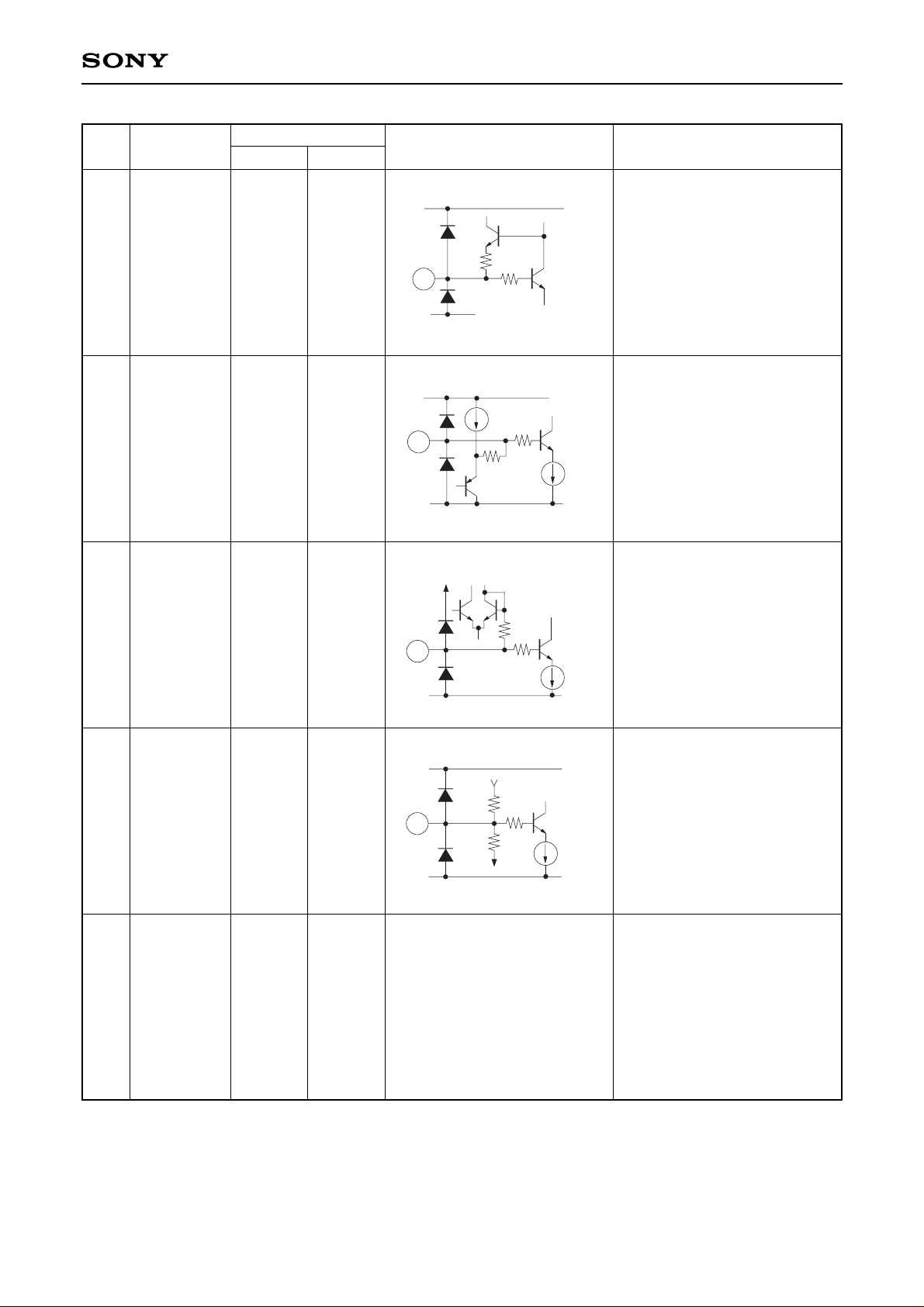
Equivalent circuit Description
ALC time constant pin.
ALC is OFF when this pin is
connected to GND.
EVR control pin for fader. 0 to
0.5 V with fixed gain.
Increasing the applied voltage
lowers the gain and causes the
fader to operate.
500
VCC1
GND
250
1k
2µ
1
50k
VCC1
GND
20µ
50k
1.24V
3
—4—
CXA2038R
Pin
No.
6
7
8
9
10
Symbol
IREF
IFDC
RFDC
VCT TC
GND1
Pin voltage
DC AC
1.17 V —
1.90 V —
1.88 V —
1.83 V —
0 V —
Equivalent circuit Description
Pin for generating the
reference current.
Connect a 47 kΩ external
resistor.
Be careful not to cause cross
talk.
Signal path DC monitor pin.
Signal path DC monitor pin.
IC internal bias pin.
Connect a decoupling
capacitor.
Audio system GND pin.
192
VCC1
GND
192
6
40k
VCCH
GND
1k
40µ
7
26.8k
VCC1
GND
1k
60µ
8
VCC1
GND
50µ
1k
60k
60k
9
∗1
∗1
Externally applied voltage

—5—
CXA2038R
Pin
No.
11
12
13
14
15
Symbol
WEIGHT
NRDC
TCH
TC
NC
Pin voltage
DC AC
1.18 V —
1.68 V —
0.47 V —
1.1 V —
— —
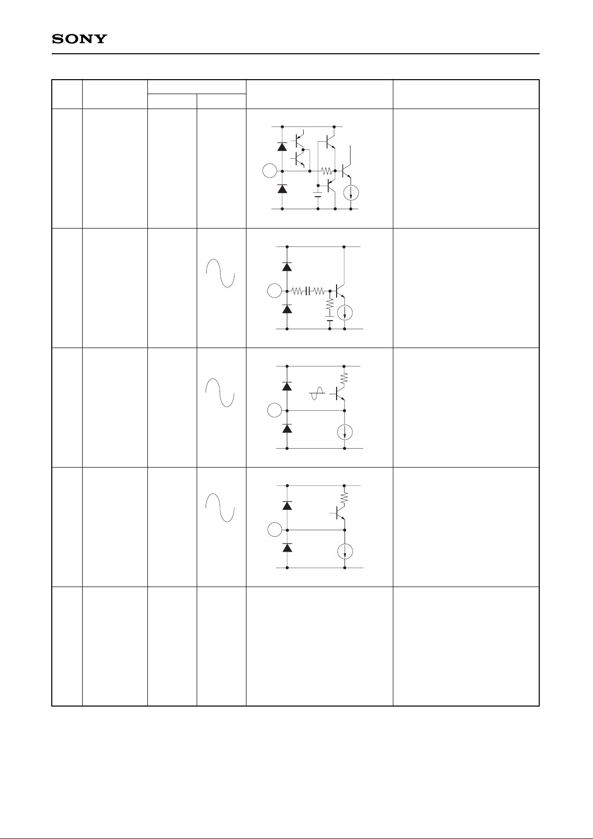
Equivalent circuit Description
NR WEIGHT time constant pin.
NR block DC monitor pin.
NR attack/recovery time
constant pins.
VCC1
GND
4.7k
5µ
11
VCC1
GND
5µ
147 1k
12
VCC1
147
150
2µ
200
10µ
GND
13
14

—6—
CXA2038R
Pin
No.
16
17
18
19
20
Symbol
NC
SI/PA
(SP/LP)
VCT
NC
NC
Pin voltage
DC AC
— —
— —
1.23 V —
— —
— —
Equivalent circuit Description
Serial/parallel (SP/LP) mode
switching pin. When this pin is
4.3 V or more, the IC operates
in serial control mode and
mode control for the IC is
performed by Pins 58 (CS), 59
(CK) and 60 (SI). When this
pin is 3.5 V or less, the IC
operates in parallel control
mode as follows.
IC internal bias pin.
Connect a decoupling
capacitor.
VCCH
GND
147
4V
50k
1.5V
10µ
20µ
SP/LP
SI/PA
17
VCC1
GND
1k
40µ
5µ
18
L (0 to 1 V) LP
H (2 to 3.5 V) or OPEN SP
—7—
CXA2038R
Pin
No.
21
22
23
24
25
Symbol
RFAGC TC
PBRFIN
BPFMONI
RECFMOUT
NC
Pin voltage
DC AC
2.3 V —
—
1.0 V
0.9 V
— —
Equivalent circuit Description
Pin for deciding RFAGC time
constant.
Input pin for PB RF signal.
The reference input level is
approximately 200 mVp-p
(Y + C + AFM).
Note that the reference input
level for the AFM component is
15 mVp-p.
Pin for monitoring the BPF
output.
Connect a 4.7 kΩ external
resistor.
Recording FM modulated
audio output pin.
VCC2
GND
1k
40µ
VCC-1.1V
21
VCC2
GND
147
VCC-1.15V
17k
17k
50µ
22
VCC2
GND
1.5M BPF OUT
20µ
100
23
VCC2
GND
220µ
100
24
Reference
input AFM
15 mVp-p
Reference
output
110 mVp-p
1.5 MHz
Reference
output
210 mVp-p

—8—
CXA2038R
Pin
No.
26
27
28
29
30
Symbol
BPF f0 ADJ
MUTETC
NTSC/PAL
FSC IN
NC
Pin voltage
DC AC
See
attached —
sheet.
2.3 V —
— —
1.53 V
— —
Equivalent circuit Description
Pin for varying the BPF fo.
Non-adjusting mode when 0 to
0.8 V (VCC = 3.15 V).
Time constant pin for
determining the MUTE OFF
delay time.
NTSC/PAL switching pin
during parallel mode.
fsc input pin.
The input level is 200 to 500
mVp-p.
During NTSC: 3.579545 MHz
During PAL: 4.433619 MHz
VCC2
GND
20µ
47k
23k
1k
73k
20µ
V
CC2/3
ADJ ON/OFF
26
VCC2
GND
10k
10µ
1k
DOC 0.6µ
DOC 2.5µ
27
VCC1
GND
50k
40µ
28
VCC2
GND
147
40µ
40k
V
CC-1.4V
29
Reference
input
300 mVp-p
L (0 to 1 V) PAL
H (2 V to VCC1) NTSC

—9—
CXA2038R
Pin
No.
31
32
33
34
35
Symbol
RFSWP
NC
BPFMONI
CTL
PLLLPF
LPEMP TC
Pin voltage
DC AC
—
— —
— —
— —
1.87 V —
Equivalent circuit Description
RFSWP input pin.
BPF ON/OFF switch control
pin.
PLL time constant pin.
Since this pin has a small
attraction and discharge
current, signals should be
received with high impedance
when monitoring this pin. Also,
be careful not to cause cross
talk.
LPEMP time constant pin.
Be careful not to cause cross
talk.
VCC2
GND
50k147
110k
1.2V
31
GND
10µ
147
4V
VCC1
33
VCC2
GND
1k
0.08µ
25k
0.08µ
34
VCC2
GND
173k
410k
35
30Hz
Input
30Hz
H (2 to V
CC1)
L (0 to 1V)
L (0 to 3.5 V) or OPEN BPF ON
H2 (4.3 V to VCCH) BPF OFF
 Loading...