

Sony CXA2032Q Datasheet

—1—
E95840-TE
Sony reserves the right to change products and specifications without prior notice. This information does not convey any license by
any implication or otherwise under any patents or other right. Application circuits shown, if any, are typical examples illustrating the
operation of the devices. Sony cannot assume responsibility for any problems arising out of the use of these circuits.
Absolute Maximum Ratings (Ta=25 °C)
• Supply voltage VCC 7V
•Operating temperature Topr –10 to +75 °C
• Storage temperature Tstg –65 to +150 °C
• Allowable power dissipation
PD 450 mW
Operating Condition
Supply voltage VCC 4.5 to 5.25 V
Description
The CXA2032Q is a bipolar IC designed as
recording/playback amplifiers for 8 mm VTRs.
Features
Recording system
• Supports EVR control for recording Y/low-band
recording level
• Feedback damping circuit provided in the
recording amplifier
Playback system
• Feedback damping circuit provided in the playback
amplifier facilitates printed circuit board design
• RFAGC and dropout detection circuit
Applications
8 mm VTR
Structure
Bipolar silicon monolithic IC
2-channel REC/PB Amplifier for 8 mm VTR
32 pin QFP (Plastic)
CXA2032Q

—2—
CXA2032Q
Block Diagram and Pin Configuration
LOGIC
BUFF
AGCDET
DOCDET
1
1
7 6 5 4 3 28 1
9
10
11
12
13
14
16
15
17 18 19 20 21 22 23 24
25
26
27
28
29
30
31
32
RFAGCTC
RFAGCOUT
DOCDET
DOP
BOTH REC
RFSWP
RP PB
YLEVEL
RFAGCIN
VREG
PBRFOUT
V
CC
VOUT1
REC1IN
RECDUMP1
V
CC1
REC1OUT
PB1IN
GND1
PBDUMP1
PBDUMP2
GND2
PB2IN
REC2OUT
YIN
CLEVEL
CIN
GND
VOUT2
REC2IN
RECDUMP2
V
CC2
CXA2032Q
RFSW
1CH
6dB
2CH
15dB
REC1CH
40dB
HEAD
REC
2ND
40dB 15dB
REC2CH
HEAD
2ND
REC
YGCA
CGCA
RFA GC

—3—
CXA2032Q
Pin Description (VCC, VCC1ch, VCC2ch=4.75 V Ta=25 °C)
Pin
No.
1
2
3
4
Symbol
YLEVEL
RP PB
RFSWP
BOTH REC
0 V
to
4.75 V
input
H: 2.3 V
or more
L: 0.6 V
or less
input
H: 2.3 V
or more
L: 0.6 V
or less
input
H: 2.3 V
or more
L: 0.6 V
or less
input
Description
EVR adjusting pin for Y
signal level during
recording. The control
voltage is from 0 V to 4.75
V.
Increasing the input
voltage increases the Y
signal level.
Input pin for REC/PB
mode switching signal.
H: PB
L: REC
Input pin for RFSWP
signal.
Alternate recording/both
channel recording
switching pin.
H: Both channel recording
L: Alternate recording
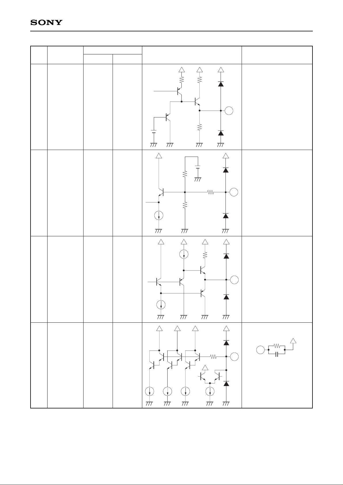
Equivalent circuit
Pin voltage
DC AC
—
—
—
—
79.5k 140
37µ
1
80k 140
10µ
1.4V
2
80k 140
10µ
1.4V
3
80k 140
10µ
1.4V
4
—4—
CXA2032Q
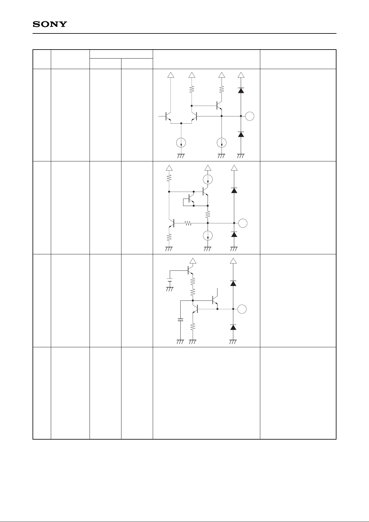
Pin
No.
5
6
7
8
Symbol
DOP
DOCDET
RFAGCOUT
RFAGCTC
Pin voltage
DC AC
H: 3.15 V
L: 0.0 V
output
2.6 V
(when pin
is open)
2.8 V
2.5 V
to
4.75 V
input
(during
EVR
adjustment)
—
—
400mVp-p
output
—
Equivalent circuit
150
2.4k
3.1V
5
4.15V
50µ
140
26.3k
43.4k
6
600µ
100
40µ
410µ
7
50µ50µ25µ25µ
140
8
Description
Output pin for dropout
detection signal. Goes
High during dropout.
Pin for deciding dropout
detection level. Connect
decoupling capacitance
between this pin and
GND. For adjustment,
input voltage proportional
to Pin 10 (VREG) output
voltage. Increasing the
input voltage increases
the detection level.
Output pin for playback Y
signal.
RFAGC time constant pin.
RFAGC gain can be
adjusted by EVR.
Increasing the input
voltage increases the
gain.
VCC
4700P
8
470k

—5—
CXA2032Q
Pin
No.
9
10
11
12
Symbol
RFAGCIN
VREG
PBRFOUT
VCC
Pin voltage
DC AC
—
4.15 V
2.0 V
4.75 V
220mVp-p
input
—
220mVp-p
(playback
Y signal
output)
—
Equivalent circuit
50k
50µ
14013P
3.25V
9
10
360µ
100
35µ
290µ
11
Description
Input pin for playback Y
signal. Playback Y signal
is separated from
playback video signal
output to Pin 11
(PBRFOUT), then input to
Pin 9 (RFAGCIN).
Output pin for 4.15 V
regulator. Connect
decoupling capacitance
between this pin and
GND.
Output pin for playback
video signal.
Power supply pin for main
blocks excluding
recording and head
amplifiers.
—6—
CXA2032Q
Pin
No.
13
14
15
16
Symbol
VOUT1
REC1IN
RECDUMP1
VCC1
Pin voltage
DC AC
3.4 V
0.7 V
1.4 V
4.75 V
184mVp-p
(recording
Y signal
output)
120 µAp-p
input
—
—
Equivalent circuit
150µ
100
400µ
13
100
300µ
300µ
100
14
7.5k
7.5k
7.5k
4.15V
15
Description
Recording video signal
1ch output pin.
The signal obtained by
mixing the recording Y,
recording C, recording
AFM and recording ATF
signals is output.
Recording video signal
1ch REC AMP input pin.
Pin 13 (VOUT1) output is
V/I converted by external
resistor, then input to Pin
14 (REC1IN).
Damping adjusting pin for
1ch recording amplifier.
Damping is adjusted by
attaching damping
resistor between Pin 15
and GND.
Decreasing the resistance
value increases the
damping.
Power supply pin for 1ch
recording and head
amplifiers.
 Loading...