

SONY CXA2019A Diagram

– 1 –
CXA2019AQ
40 pin QFP (Plastic)
E98320-PS
NTSC/PAL Chroma Decoder
Description
The CXA2019AQ is a bipolar IC which integrates
the luminance signal processing, chroma signal
processing, and sync signal processing functions for
NTSC/PAL system color TVs onto a single chip.
Features
• Sub picture bright and white balance can be
adjusted by using the main picture Y/C/J BGP
output as the timing pulse
• I2C BUS compatible; two bus lines (SCL, SDA)
allow various adjustments and user controls
• Countdown system eliminates need for H and V
oscillator frequency adjustment
• Non-adjusting Y system filters (chroma trap, delay
line)
• Automatic identification of color system (forced
control possible)
• Automatic identification of 50/60Hz vertical frequency
(forced control possible)
• Built-in delay line aperture correction
• Built-in dynamic picture (black expansion) function
• Combination with a non-adjusting SECAM chroma
decoder allows configuration of multiple systems
Absolute Maximum Ratings
(Ta = 25°C, SGND, JGND = 0V)
• Supply voltage VCC 12 V
• Operating temperature Topr –20 to +75 °C
• Storage temperature Tstg –65 to +150 °C
• Allowable power dissipation PD 1.67 W
Operating Conditions
Supply voltage VCC 9 ± 0.5 V
Applications
Color TVs
Structure
Bipolar silicon monolithic IC
Sony reserves the right to change products and specifications without prior notice. This information does not convey any license by
any implication or otherwise under any patents or other right. Application circuits shown, if any, are typical examples illustrating the
operation of the devices. Sony cannot assume responsibility for any problems arising out of the use of these circuits.
– 2 –
CXA2019AQ
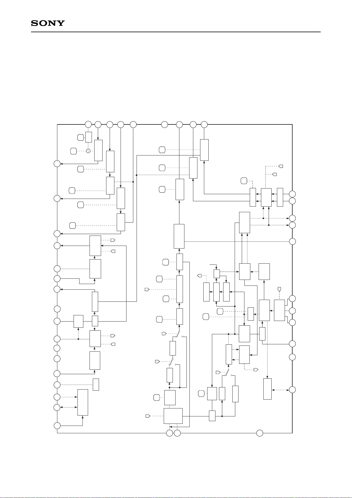
Block Diagram
1
2
4
5
6
7
8
9
10
11
12
13
14
15
16
17
18
19
20
21
22
23
24
25
26
2728
29
30
40
39
38
37
36
35
34
31
32
33
V OUT
U OUT
Y OUT
SGND2
SCP
H TIM
V TIM
V2 IN
U2 IN
Y2 IN
S GND
CIN
A PED
CVBS/Y IN
ADRS
SCL
SDA
V SYNC
H SYNC
V HOLD
SECAM REF
APC
X 443/358
X 358
X NTSC
SV
CC
– (R_Y) OUT
– (B_Y) OUT
– (B_Y) IN
– (R_Y) IN
CERA
AFC
IREF
J GND
V2 OUT
U2 OUT
Y2 OUT
ABLFILIN
CP IN
∗
The sub picture bright and white balance
can be adjusted by receiving BGP or
SCP output from the main picture Y/C/J,
clamping the PINP PROC. output, and
varying the DC of the clamped portion.
I
2
C BUS
DECORDER
IREF
H.SYNC
SEP
PHASE
DET.
1/32 H.DRIVE
32f
H
VCO
V.SYNC
SEP
V COUNT
DOWN
V2 PED
V2 DRIVE
U2 PED U2 DRIVE
Y2 DRIVE
ABL
Y DRIVE
U PED
V PED
AUTO
PEDESTAL
CLAMP
DELAY SHARPNESS
TRAP
TRAP
SUB
CONT
VIDEO
SW
BST AMP
COLOR
KILLER
PHASE
DET.
HUE
LPF
SECAM
CHROMA
VCO
4.43/3.58
SW
NT/PAL
PAL ID
ID AXIS
F.F
DEM
AXIS
PHASE
SHIFT
CHROMA
DET.
DET
SW
COLOR
CLAMP
ACC
DET.
ACC
DELAY
TOT
ABL CENT
Y2 DRIVE
U2 DRIVE
U2 PED
V2 DRIVE
V2 PED
50/60C MODEAFC HLOCK
2f
H
V PEDU PEDY DRIVE
DC TRAN
SHARPNESS
SHP f0
PRE OVER
DELAY
TRAP ON
SECAM
SUB CONT
CV/YC
COLOR
NT/PAL
EXT COLOR
2f
H
NT/PAL
HUE
SUB HUE
X'TAL PIN
KILLER
TOT ON
SUB COLOR
3
J Vcc
– 3 –
CXA2019AQ
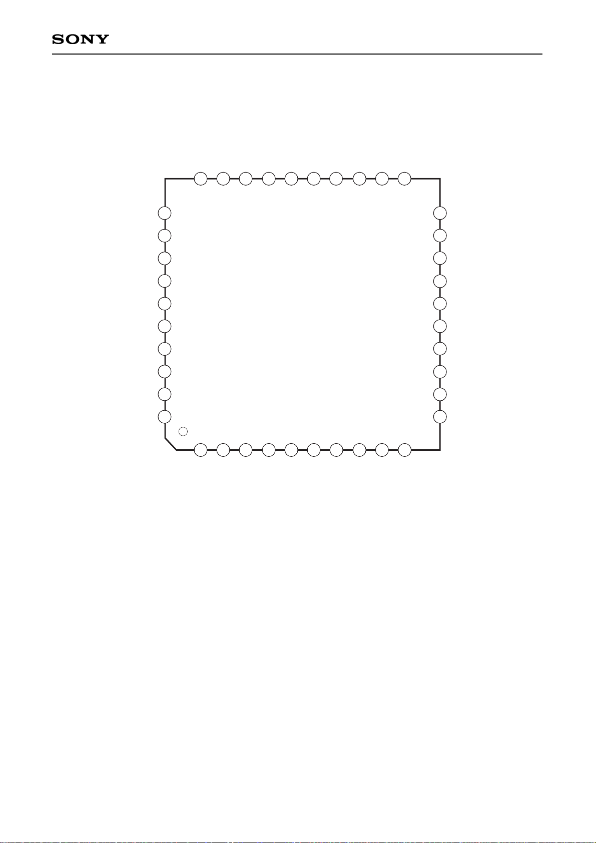
Pin Configuration
1
2
3
4
5
6
7
8
9
10
11
12
13
14
15
16
17
18
19
20
21
22
23
24
25
2627
28
29
30
40
39
38
37
36
35
34
31
32
33
V OUT
U OUT
Y OUT
SGND2
SCP
H TIM
V TIM
V2 IN
U2 IN
Y2 IN
S GND
CIN
A PED
CVBS/Y IN
ADRS
SCL
SDA
V SYNC
H SYNC
V HOLD
SECAM REF
APC
X 443/358
X 358
X NTSC
SV
CC
– (R_Y) OUT
– (B_Y) OUT
– (B_Y) IN
– (R_Y) IN
CERA
AFC
JV
CC
IREF
J GND
V2 OUT
U2 OUT
Y2 OUT
ABLFILIN
CP IN
– 4 –
CXA2019AQ
32fH (500 or 503.5kHz) ceramic
oscillator connection.
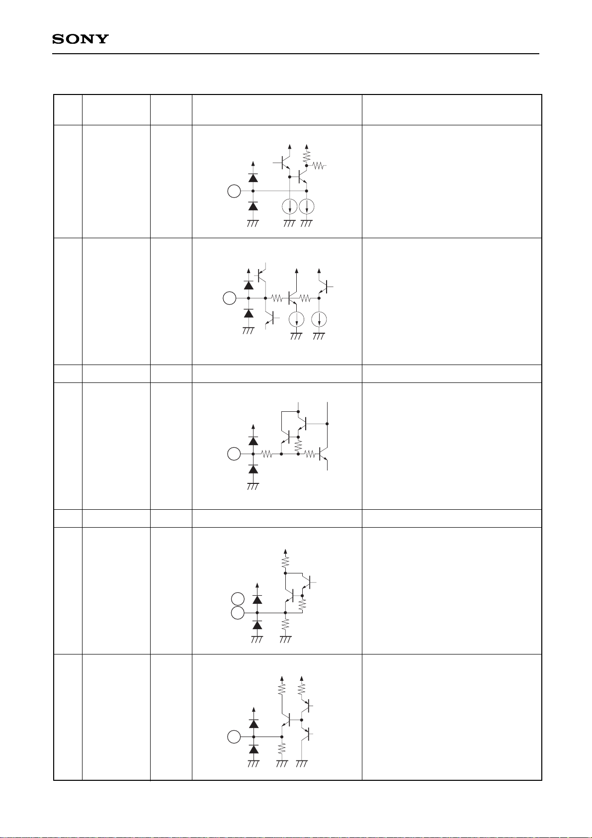
Pin Description
Pin
No.
Symbol Equivalent circuit Description
1
CERA
2
AFC
CR connection for AFC lag-lead filter.
4
IREF
Connect a 10kΩ resistor between this
pin and GND.
6
7
V2 OUT
U2 OUT
Reinput system outputs.
8
Y2 OUT Reinput system output.
3
JVCC
5
—
—
1.8V
3V
3V
9.0V
—
J GND
Power supply.
Jungle system (H/V) GND.
VccVcc
10k
28k
Vcc
1
46k
Vcc
2
1.2k
Vcc Vcc
14.4k
Vcc
150
4
20k
8.6k
Vcc
20k
Vcc
200
7
6
8k
Vcc
4k
Vcc
200
Vcc
8
Pin
voltage
– 5 –
CXA2019AQ
Reinput system clamp pulse input.
Input the main picture BGP (SCP).
Vth: 2.5V
Pin
No.
Symbol Equivalent circuit Description
9
ABLFILIN
ABLFIL voltage input.
Input the main picture Y/C/J ABLFIL
voltage.
10
CP IN
11
12
13
Y2 IN
U2 IN
V2 IN
Reinput system inputs.
Input via a capacitor.
14
V TIM
V timing pulse output.
Outputs a 0 to 5V positive polarity
pulse.
37k
Vcc
90k
Vcc
90k
9
Vcc
1.2k
Vcc
15k
10
11
13
1.2k
Vcc
70k
12
20k
Vcc
Vcc
1k
14
1k
15
—
—
4V
—
—
H TIM
H timing pulse output.
Outputs a 0 to 5V positive polarity
pulse.
20k
Vcc
Vcc
1k
1k
15
Pin
voltage
– 6 –
CXA2019AQ
GND.
Pin
No.
Symbol Equivalent circuit Description
16
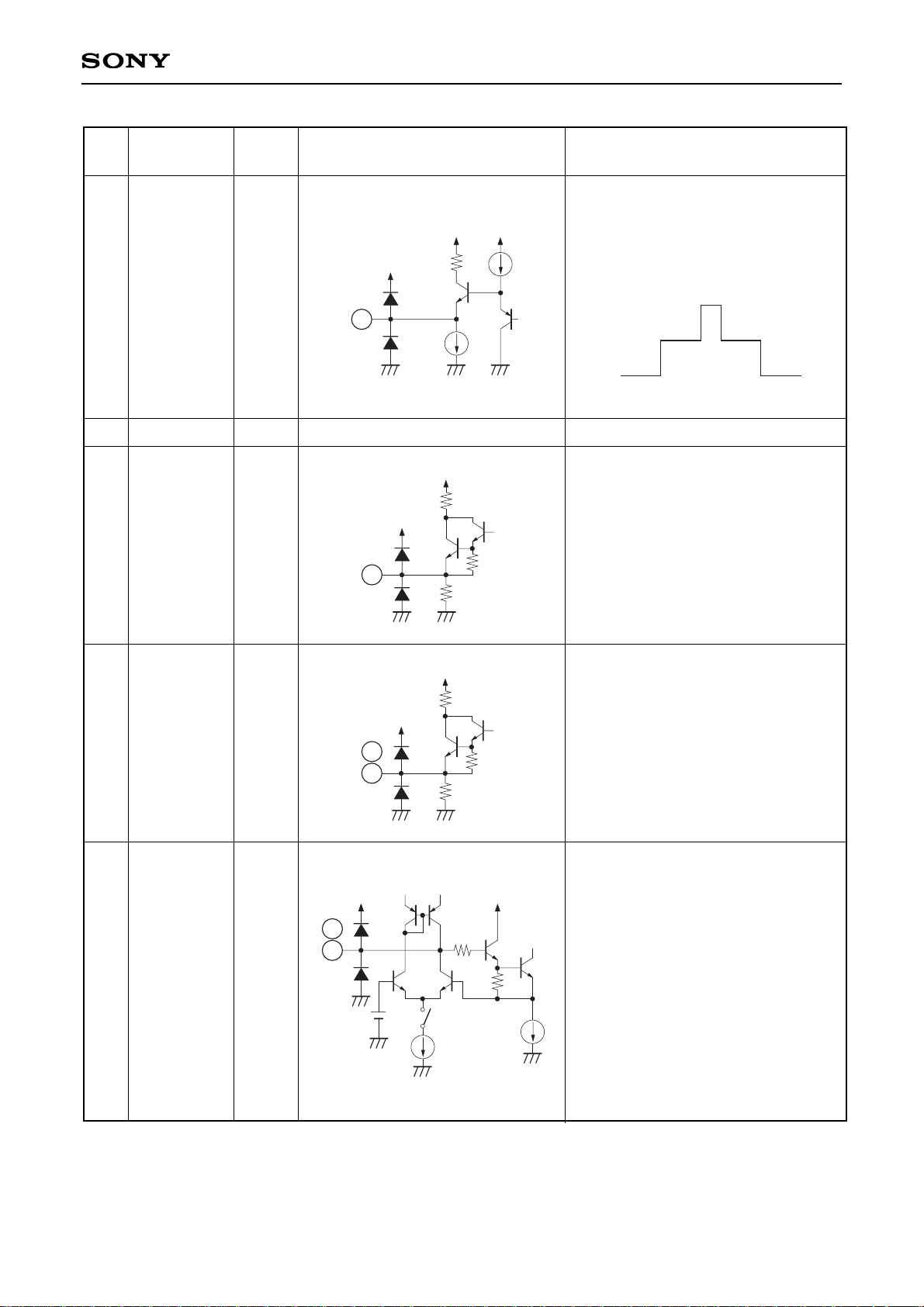
SCP
Outputs BGP and HBLK as SCP
(sand castle pulse).
The typ. waveform is as follows.
Vcc
Vcc
1.2k
Vcc
500µA
16
18
Y OUT
Y (luminance signal) output.
Standard output level: 1.1Vp-p
6k
Vcc
20k
Vcc
200
18
19
20
U OUT
V OUT
U/V (color difference signal) outputs.
Output level: U = V = 1.2Vp-p
(In case of setting data as shown in
"I2C BUS Register Initial Settings.")
19
8.6k
Vcc
20k
Vcc
200
20
21
22
– (R_Y) IN
– (B_Y) IN
Color difference signal inputs. Input
as negative polarity via a capacitor.
Standard input levels:
B-Y: 1.33Vp-p
R-Y: 1.05Vp-p
21
Vcc
1.2k
Vcc
70k
22
100µA
BGP
17
—
3V
3V
5.6V
—
SGND2
Pin
voltage
HBLK
BGP
5.0V
2.0V
0.3V

– 7 –
CXA2019AQ
Power supply.
Pin
No.
Symbol Equivalent circuit Description
23
24
– (B_Y) OUT
– (R_Y) OUT
Color difference signal outputs.
Output as negative polarity.
Standard output levels:
B-Y: 0.665Vp-p
R-Y: 0.525Vp-p
23
Vcc Vcc Vcc
24
1.2k
26
27
28
X NTSC
X 358
X443/358
Crystal oscillator connections.
Connect the PALN and 4.43MHz
crystal to Pin 28.
Connect the PALM crystal to Pin 27,
and the NTSC crystal to Pin 26.
26
28
Vcc
Vcc
4k
500
27
29
APC CR connection for APC lag-lead filter.
Vcc
1.2k
Vcc
1.2k
25k
29
30
SECAM REF
When the IC is set to SECAM
identification mode, the 4.43MHz VCO
oscillator waveform is output from this
pin centering on DC 1.5V.
If a 150µA current is led from this pin
during this identification mode, the IC
is set to SECAM mode. In SECAM
mode, the 4.43MHz VCO oscillator
waveform is output centering on
DC = 5V only during the VBLK
interval.
Vcc
40k
6k
Vcc Vcc
10p
30
25
SVCC
Pin
voltage
31
5.6V
—
—
1.5V
9.0V
—
S GND
GND.

– 8 –
CXA2019AQ
This pin is used to switch the slave
address.
Vcc: 9AH
GND: 9EH
Vth = 2.5 V
35
Pin
No.
Symbol Equivalent circuit Description
32
C IN
Chroma signal input.
Standard input level (burst level)
: 570mVp-p
33
A PED
Black peak hold for auto pedestal (black
expansion). Connect a capacitor.
Vcc
30k
10p
32
30k
Vcc
1.2k
Vcc
16k
20k
20k
Vcc
Vcc
33
34
—
—
—
—
CVBS/Y IN
Y signal input. Input via a capacitor.
Standard input level: 2Vp-p
Vcc
1.2k
1.2k
1.2k
70k
34
Vcc
ADRS
35
Vcc
30k
77k
Pin
voltage

– 9 –
CXA2019AQ
V sync separation input. Input a 2Vp-p
video signal via a capacitor and
resistor.
V HOLD
Pin
No.
Symbol
Equivalent circuit
Description
36
37
SCL
SDA
I2C BUS SCL (Serial Clock) and SDA
(Serial Data).
Vilmax = 1.5V
Vihmin = 3V
Volmax = 0.4V
38
V SYNC
36
4k
4k
Vcc
37
Vcc
15k
20µA
150
38
24k
33k
39
H SYNC
H sync separation input. Input a 2Vp-p
video signal via a capacitor and
resistor.
Vcc
14k
10µA
150
24k
20k
39
40
—
3.5V
2.5V
—
Peak hold for V sync separation.
Connect a capacitor.
Vcc
50k
1k
150
55k
40
Pin
voltage
 Loading...