Sony CXA2016S Datasheet

—1—
E95422B78-TE
Sony reserves the right to change products and specifications without prior notice. This information does not convey any license by
any implication or otherwise under any patents or other right. Application circuits shown, if any, are typical examples illustrating the
operation of the devices. Sony cannot assume responsibility for any problems arising out of the use of these circuits.
Sync Identification for CRT Display
22 pin SDIP (Plastic)
CXA2016S
Absolute Maximum Ratings (Ta=25°C)
• Supply voltage VCC 12 V
• Operating temperature Topr –20 to +75 °C
• Storage temperature Tstg –65 to +150 °C
• Allowable power dissipation
PD 962 mW
Operating Conditions
Supply voltage VCC 5 ± 0.25 V
Description
The CXA2016S is used for sync signal
identification and waveform shaping in the CRT
computers display for multi-scan system. There are
three types of sync input signals for identification:
separate sync, composite sync, and sync on video
signals.
Features
• Power save function available (5 V power supply)
• Clamp pulse output position selectable among sync
interval, back porch interval, and AUTO.
• Polarity information of sync signals is output.
• Polarity and amplitude of input signals:
Polarity
Amplitude (Vp-p)
V. separate sync: Positive/Negative 1 to 5
H. separate sync: Positive/Negative 1 to 5
Composite sync: Positive/Negative 1 to 5
Sync on video:
Sync signals part of Negative 0.2 to 0.4
Video part 0 to 1.4
Applications
CRT display monitor
Pin Configuration (Top View) Block Diagram
1
2
3
4
5
6
7
8
9
10
11 12
13
14
15
16
17
18
19
20
21
22
VS IN
PVC
EVC
CS IN
PHC
EHC
Video IN
HD SEL
ISC
ISJ
GND
V
CC
VD
V
SS IN
V
SS OUT
HD
PV
PH
CLP SEL
CLP OUT
V
SS REF
CLP OUT
Polarity
Check
V. Ramp
Generator
Exist
Check
Polarity
Check
Exist
Check
Sync
Sep
Level
Control
Bias
Sync
Check
Logic
Clamp
Pulse
Generator
21
8
18
9
13
14
15
10 19 20 12 2211
1
17
16
4
5
6
7
2 3
PVC EVC
VS IN
PV
PH
CS IN
PHC
EHC
Video IN
ISJ VSS OUT VSS IN VSS REF GND VCC
VD
HD SEL
HD
ISC
CLP OUT
CLP SEL
CLP OUT

—2—
CXA2016S
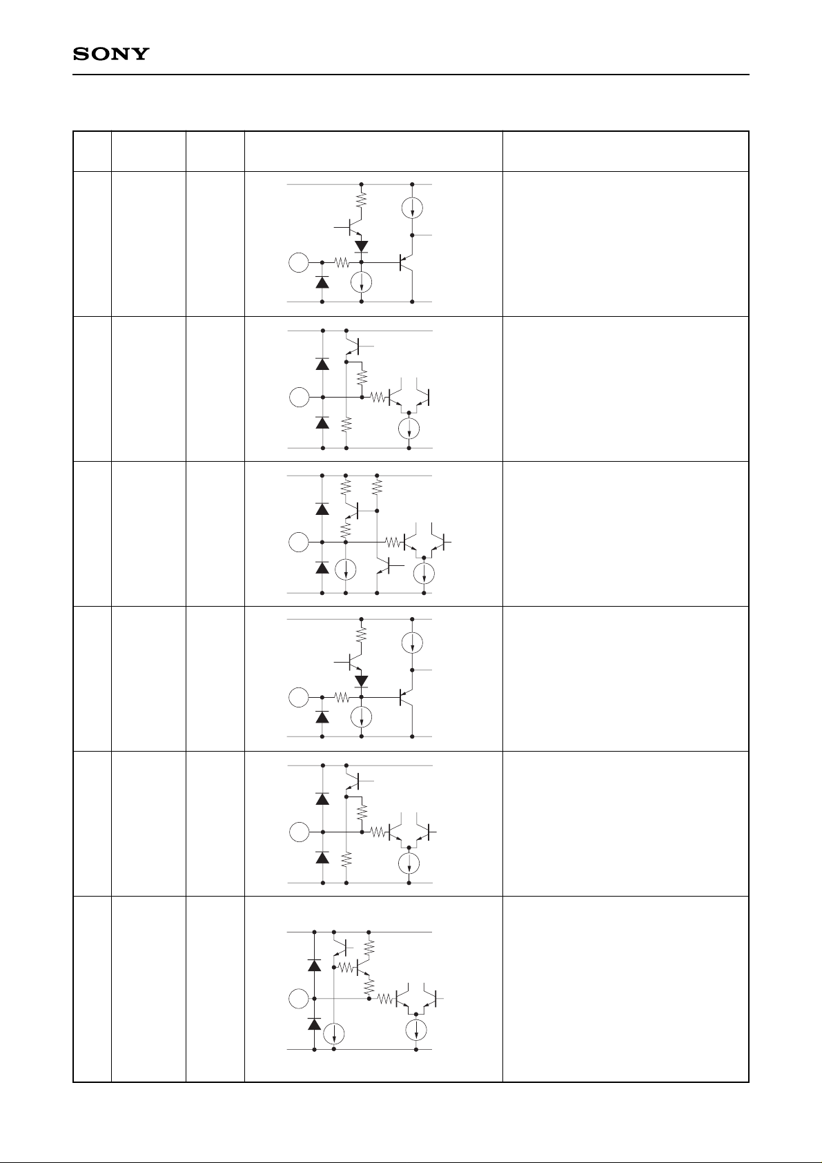
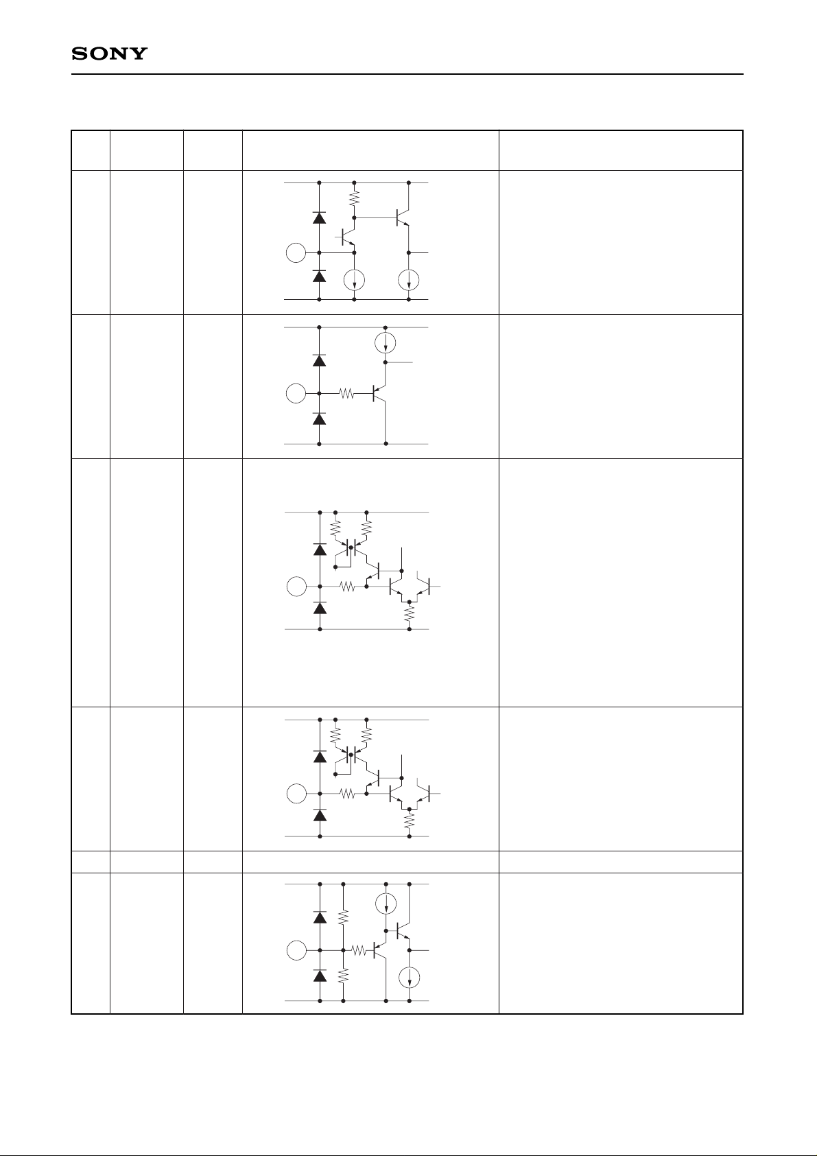
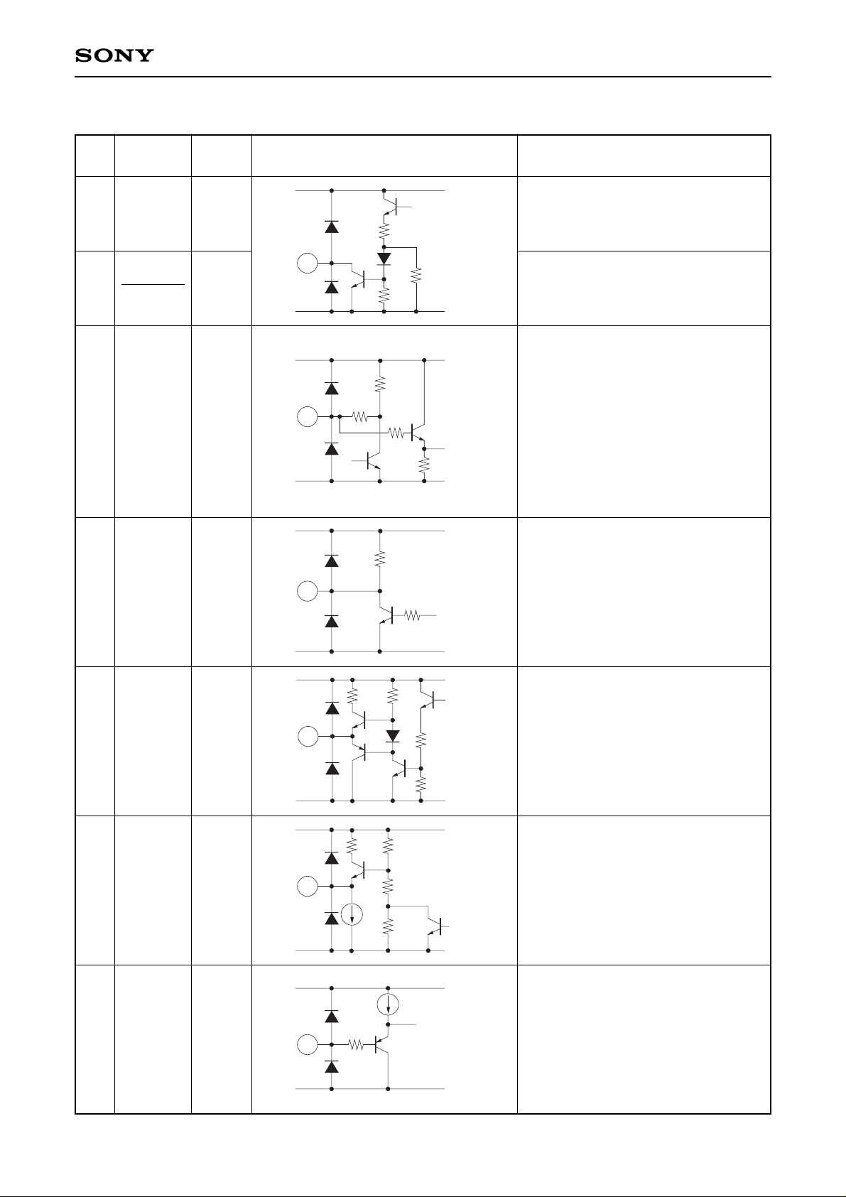
Pin Description (Ta=25 °C, VCC=5 V)
Pin
Symbol
Pin
Equivalent circuit Description
No voltage
VCC
GND
1
100
1k
VCC
GND
2
1k
96k
8k
1k
3
200
200
200
1k
VCC
GND
VCC
GND
100
1k
4
VCC
GND
96k
8k
1k
5
6
1k
100
1k
1k
VCC
GND
VS IN
PVC
EVC
CS IN
PHC
EHC
2.6 V
—
—
2.6 V
—
—
V. separate sync (positive/negative
polarity) as capacitor input. Amplitude
is 1 to 5 Vp-p.
This pin connects a 0.22 µF
integrating capacitor for the vertical
signal polarity check circuit to GND.
When connecting the capacity at
positive polarity, it is 2.9 V and at
negative polarity, 120 mV.
V. ramp waveforms generation part of
vertical signal exist check circuit.
Generates ramp waveforms
synchronously with the input signal
cycle and connects 0.22 µF to GND.
Inputs composite sync
(positive/negative polarity) and H.
separate sync (positive/negative
polarity) as capacitor input. Amplitude
is 1 to 5 Vp-p.
This pin connects a 0.1 µF integrating
capacitor for the horizontal signal
polarity check circuit to GND. When
connecting the capacity at positive
polarity, it is 2.6 V and at negative
polarity, 350 mV.
A 33 kΩ resistance and a nearly peak
hold circuit for 0.22 µF capacitor are
connected to this pin for input signal
exist check at CS IN input pin. When
a signal is input at CS IN pin, a nearly
peak hold is executed at 2.1 V to 2.7
V, a comparison is made with the 1.4
V reference voltage, and input signal
exist is identified.
1
2
3
4
5
6

—3—
CXA2016S
7
2k
VCC
GND
8
1k
VCC
GND
9
2k 1k
VCC
GND
50k
100
4k 1k
VCC
GND
50k
100
10
12
12k
20k
1k
VCC
GND
7
8
9
10
11
12
Video IN
HD SEL
ISC
ISJ
GND
VSS REF
—
—
1.2 V
1.2 V
0 V
3.125 V
Inputs sync on video (sync at negative
polarity). Connects in series a 1 µF
capacitor and a 270 Ω resistance to
input signals.
Selects output processing of HD
(H. Drive Pulse) at a VD interval.
Input at TTL level.
When Low level is selected, HD is not
output at a VD interval.
When High level is selected, HD is
output at the VD interval.
Resistance connecting pin for
reference current source of clamp
pulse output circuit, and connects 12
kΩ resistance to GND. When a 12 kΩ
resistance is connected, a 100 µA
current flows through this pin (pulse
width is approximately 300 ns).
Clamp pulse output pulse width is
varied by changing the value of the
resistance.
∗
Use a metal film resistor with an
accuracy of ±1 %
Resistance connecting pin for
reference current source and
connecting 12 kΩ resistance to GND.
When the resistance is connected, a
100 µA current flows through this pin.
∗
Use a metal film resistor with an
accuracy of ±1 %
GND pin.
Reference pin for V. sync separator of
composite sync and video sync.
—
Pin
Symbol
Pin
Equivalent circuit Description
No voltage

—4—
CXA2016S
13
14
15
16
17
18
19
20
CLP OUT
CLP OUT
CLP SEL
PH
PV
HD
VSS OUT
VSS IN
—
—
—
—
—
—
—
Clamp pulse output; Open collectortype pin at positive polarity.
Clamp pulse output; Open collectortype pin at negative polarity.
Selects output position of a clamp
pulse. Input at TTL level.
When Low level is selected, a clamp
pulse is output at a back porch
interval.
When High level is selected, clamp
pulse is output at a sync interval.
See the Description of Operation for
Input/Output Matrix.
Output polarity information of
horizontal and vertical sync signals.
See the Description of Operation for
Input/Output Matrix.
HD (H. Drive Pulse) output; Push-pull
type pin at positive polarity.
Composite sync or sync signal
separated from video sync is output.
Output is at positive polarity.
Input for V. sync separator
comparator. Integrates the output at
Pin 19 and inputs it.
Pin
Symbol
Pin
Equivalent circuit Description
No voltage
VCC
13
15
500
40k
7k
GND
VCC
30k
20k
1k
43k
GND
VCC
20k
16
20k
GND
18
19
20
333 6k
200 5k
1k
2.5k
17.5k
6k
6k
VCC
GND
VCC
GND
VCC
GND
 Loading...