

Sony CXA2013M Datasheet

EIAJ Sound Multiplexing Decoder
Description
The CXA2013M is a bipolar IC designed as EIAJ
TV sound multiplexing decoder, provides various
functions including sound multiplexing demodulation,
broadcast mode identification (stereo/bilingual
discrimination display), volume, tone control and
muting.
Features
• Adjustment free of filter
• Audio multiplexing decoder
• Sound processor
— One external input
— Bass control
— Treble control
— V olume control
— Balance control
are all included in a single chip. Almost any sort of
signal processing is possible through this IC.
• Separation adjustment, each mode control and sound
processor control are possible through I2C BUS.
CXA2013M
30 pin SOP (Plastic)
Absolute Maximum Ratings (Ta = 25°C)
• Supply voltage VCC 12 V
• Operating temperature Topr –20 to +75 °C
• Storage temperature Tstg –65 to +150 °C
• Allowable power dissipation PD 1000 mW
Operating Supply Voltage Range 8.5 to 9.5 V
Applications
TVs
Structure
Bipolar silicon monolithic IC
Pin Configuration
SC OUT
NC
SC IN
MC OUT
MC IN
TV OUT-L
TV OUT-RNCAUX-L
30
29
28
27
26
25
24
23
1
2
3
4
5
6
7
8
REFL
Vcc
MPX IN
GND
SUBI
Sony reserves the right to change products and specifications without prior notice. This information does not convey any license by
any implication or otherwise under any patents or other right. Application circuits shown, if any, are typical examples illustrating the
operation of the devices. Sony cannot assume responsibility for any problems arising out of the use of these circuits.
CUBI
NC
SDA
22
9
SCL
AUX-R
21
10
DGND
CL-R
20
11
BAL
CL-L
19
12
TRE
CH-R
18
13
BASS
CH-L
171516
14
VOL
LS OUT-L
LS OUT-R
– 1 –
E00Y28A1Y-PS

Block Diagram
– 2 –
SUBI
1
BIAS
CURRENT
IBIAS
2
SC OUT
30
SUBDEEM
FM
DEMOD
BUFFER
VOLTAGE
REGULATOR
SC IN
28
BIAS
VOLTAGE
3
MC OUT
27
MAINDEEM
4
26
VCA
MC IN
SUB
DET
SUB
BPF
4.5fH
TRAP
SUB
ATT
MPX SIGNAL
5
TV OUT-L24TV OUT-R21AUX-R22AUX-L17CH-L19CL-L
25
MATRIX SW
MAIN
IIL LOGIC & CONT
3.5f
3.5fH
VCO
H
CLOCK
952Hz
BPF
CUE
BPF
CUE
CARRIOR
AM
DEMOD
952Hz
CLOCK
COMP
6
TONE
BASS
TRE
TONE
18
20
VCA
VOL
BAL
VCA
DAC BUS DEC
11
12
13
14
LS OUT-L
16
LS OUT-R
15
8
9
10
GND
REFL
Vcc
MPX IN
CUBI
CH-R
CL-R
BAL
TRE
BASS
VOL
SDA
SCL
DGND
CXA2013M
CXA2013M
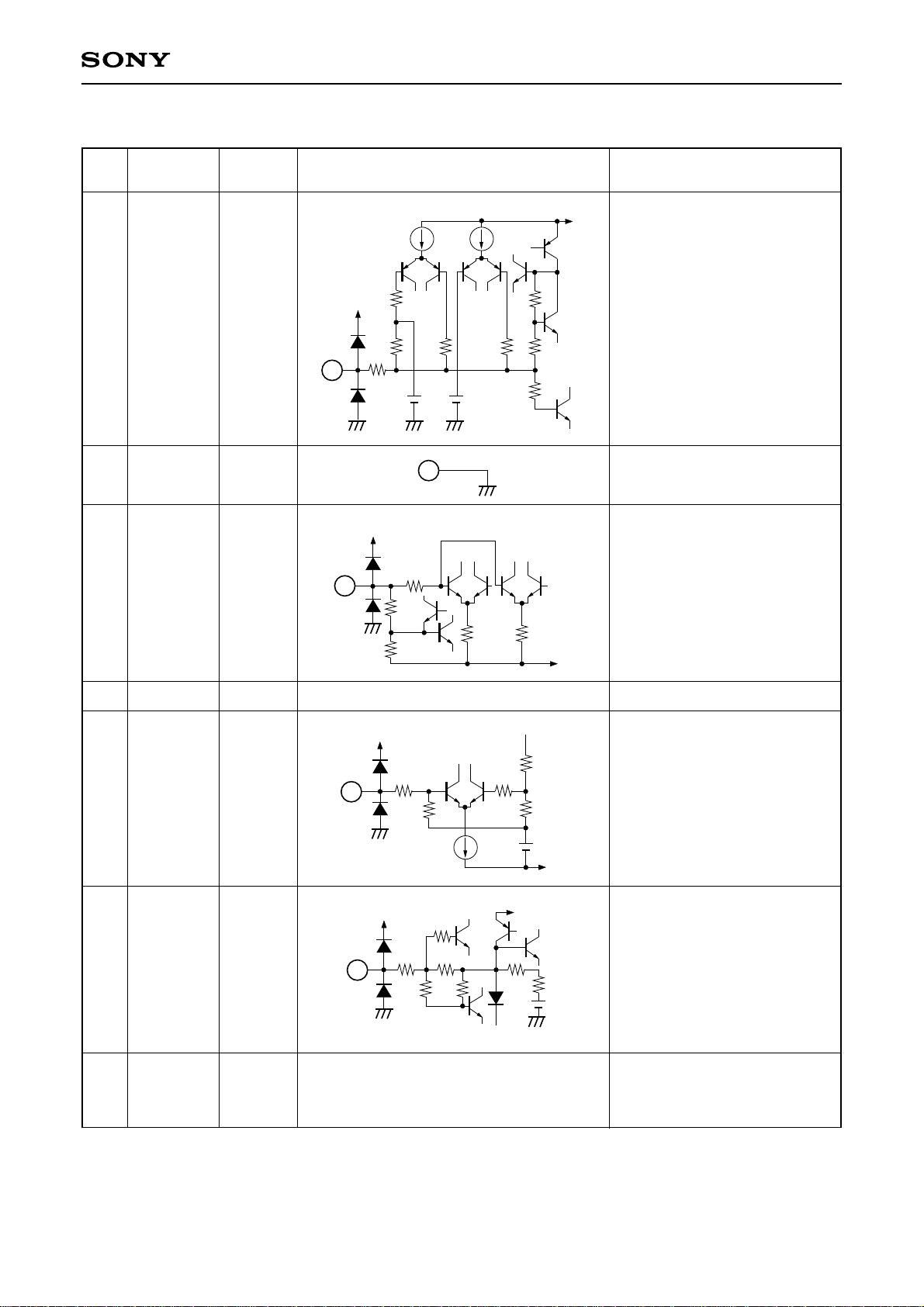
Pin Description (Ta = 25°C, VCC = 9V)
Pin
No.
Symbol
Pin
voltage
1 SUBI 4.1V
2 GND 0
3 REFL
1.2V
Equivalent circuit Description
Vcc
20µ
64k
Bias capacitor connection of
Vcc
80µ
16k
sub FM detector
4.2V
147
3.3k
24k
1k
2
8k
147
1.7V
20k 20k
8k
Analog block GND
The noise elimination filter
connection of internal
reference voltage
GND
16k
1
147
Vcc
3
4VCC —
5 MPX IN 4.1V
6 CUBI
4.1V
7,
23,
NC
29
—
Power supply
Vcc
147
5
50k
80µ
Vcc
6
147
40k
1k
40k
40k
—
27.6k
11k
Vcc
87.9k
30k
4.2V
GND
2k
4.2V
Sound multiplexing signal input.
Typical input level = 110mVrms
(monoural 100%)
Bias capacitor connection of
Cue pulse generator
—
– 3 –
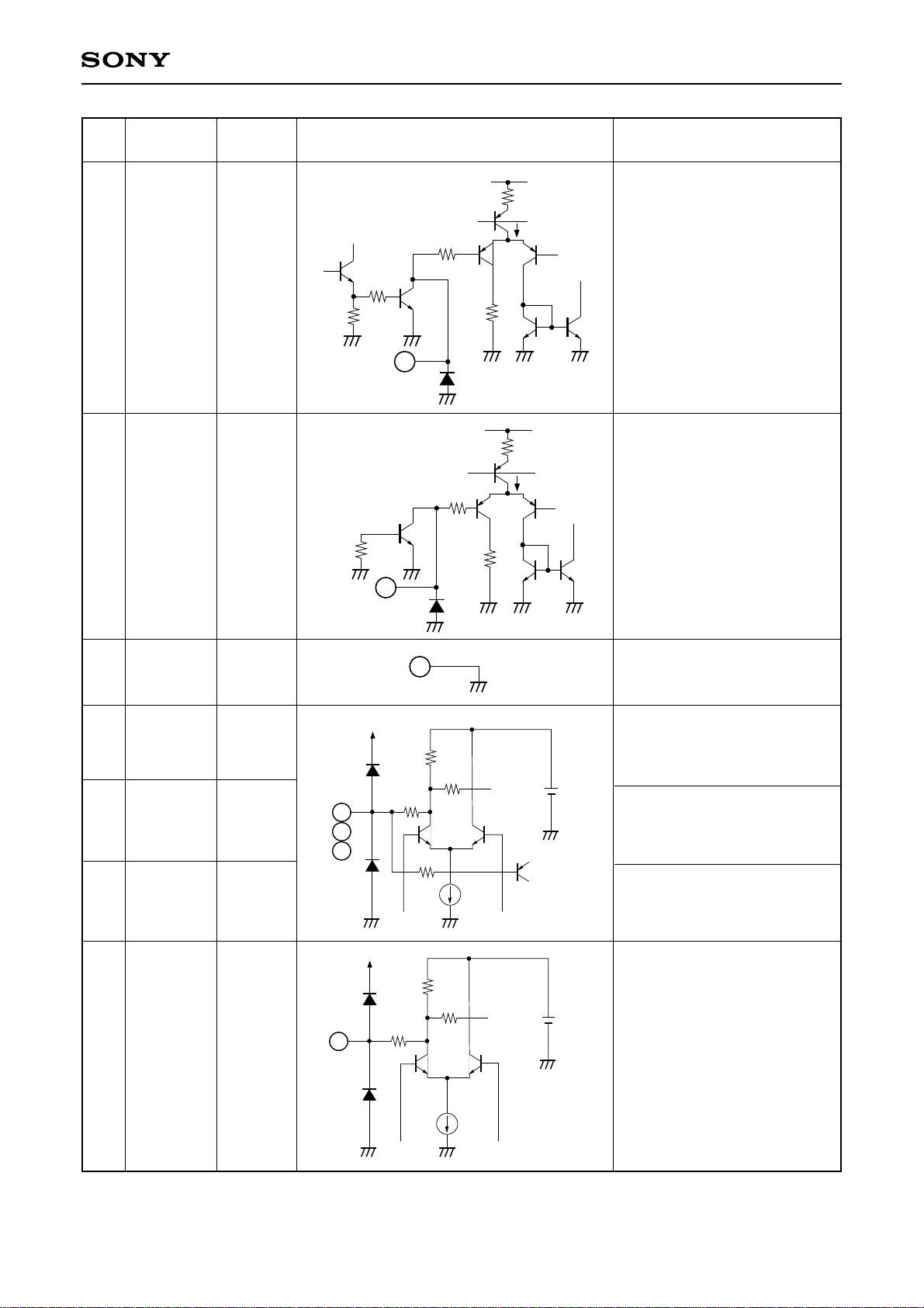
CXA2013M
Pin
No.
Symbol
8SDA
9 SCL
Pin
voltage
—
—
7.5k
10.5k
Equivalent circuit Description
V
CC
7.5k
35µ
7.5k
35µ
2.1V
2.1V
Serial data I/O pin
VIH > 3.0V
VIL < 1.5V
Serial clock I/O pin
×2
4.5k
4k
×5
8
4k
3k
V
CC
VIH > 3.0V
×4
3k
VIL < 1.5V
10 DGND
—
11 BAL 4.2V
12 TRE 4.2V
13 BASS 4.2V
14 VOL 5.2V
14
11
12
13
VCC
VCC
9
10
Digital block GND
DAC output pin. (BAL)
Connect LPF capacitance of DAC.
Internal impedance is
approximately 20kΩ.
DAC output pin. (TRE)
2k
40k
20k
5.2V
Connect LPF capacitance of DAC.
Internal impedance is
2k
approximately 20kΩ.
DAC output pin. (BASS)
75µ
Connect LPF capacitance of DAC.
Internal impedance is
approximately 20kΩ.
10k
5k
2k
5.2V
DAC output pin. (VOL)
Connect LPF capacitance of DAC.
×4
×4
Internal impedance is
approximately 5kΩ.
300µ
– 4 –

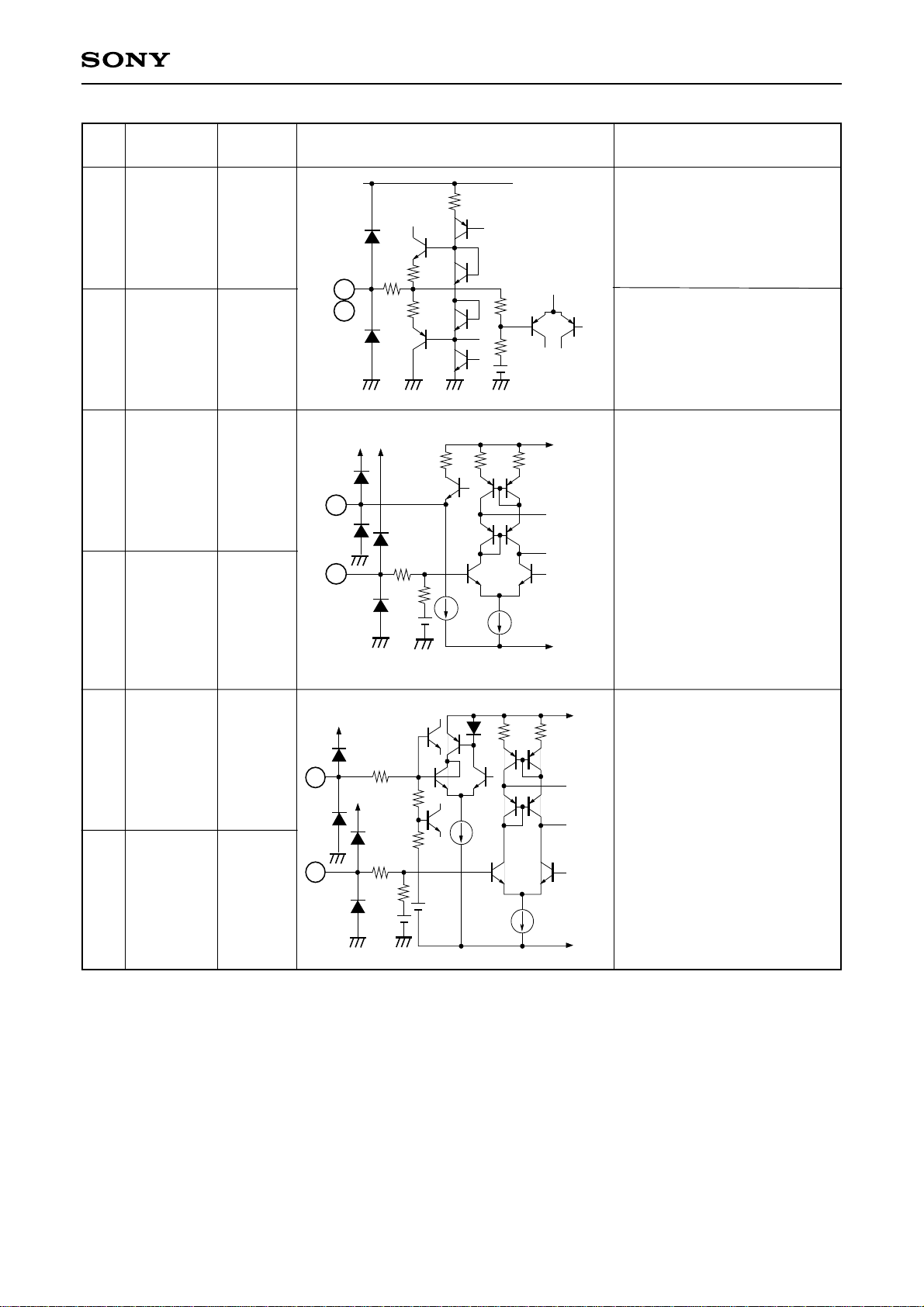
CXA2013M
Pin
No.
15 4.2V
16 4.2V
Symbol
LS OUT-R
LS OUT-L
Pin
voltage
17 CH-L 4.2V
18 CH-R
4.2V
17
18
Equivalent circuit Description
CC
V
3k
LSOUT right channel output
pin
10p
500
15
16
147
500
84k
LSOUT left channel output
pin
Vcc
250µ
250µ
Treble filter pin
(Left channel)
5.7k
147
6k
5.7k
Treble filter pin
(Right channel)
19 CL-L 4.2V
20 CL-R 4.2V
21 AUX-R 4.2V
22 AUX-L 4.2V
21
22
19
20
10.7k
147
147
250µ
36k
12k
4.2V
5.4k
250µ
12.3k
10µ
Vcc
4.2V
Vcc
Bass filter pin
(Left channel)
Bass filter pin
(Right channel)
Right channel external input
pin
Left channel external input
pin
– 5 –
CXA2013M
Pin
No.
Symbol
Pin
voltage
24 TV OUT-R 4.2V
25 TV OUT-L 4.2V
26 MC IN 4.1V
27 MC OUT 3.4V
24
25
27
26
Equivalent circuit Description
V
CC
3k
TVOUT right channel output
pin
580
147
14.3k
35.7k
4.2V
TVOUT left channel output
pin
Vcc
Vcc Vcc
580
147
8k 8k
DC cut capacitor connection
147
16k
4.2V
160µ
80µ
GND
of main signal
28 SC IN 4.1V
30 SC OUT 3.9V
30
28
Vcc
Vcc
147
147
16k
4.2V
8k
40k
4.2V
320µ
Vcc
8k8k
DC cut capacitor connection
of sub signal
80µ
GND
– 6 –

Electrical Characteristics
(Ta = 25°C, V
CC = 9V)
No. Item Symbol Mode Input signal
Current consumption
1
MPX input level
2
MPX input level
3
range
MONO output level
4
MONO frequency
5
response
MONO distortion
6
Icc
Vin
Vrange
Vmain
Fcmain
THDm
MONO
MONO
MONO
– 7 –
MONO distortion at
7
maximum input
MONO S/N
8
Sub output level
9
Sub frequency
10
response
THDmmax
SNmain
Vsub
Fcsub
MONO
MONO
BIL
BIL
Input
pin
—
5
—
5
5
5
5
5
5
5
No input
MONO 1kHz, 100% mod.
MONO 1kHz 100% mod.
Sub: Career OFF, Cue: OFF
MONO 10kHz 100% mod.
Sub: Career OFF, Cue: OFF
MONO 1kHz 100% mod.
Sub: Career OFF, Cue: OFF
MONO 1kHz 300% mod.
Sub: Career OFF, Cue: OFF
MONO 1kHz 100% mod.
Sub: Career OFF, Cue: OFF
SUB 1kHz 100% mod.
Main 0% mod., Cue: BIL
SUB 10kHz 100% mod.
Main 0% mod., Cue: BIL
—
Measurement
conditions
20 log ('10k'/'1k')
20 log ('100%'/'0%')
20 log ('10k'/'1k')
Filter
15kLPF
15kLPF
15kLPF
15kLPF
15kLPF
Output
pin
4
5
—
24/25
24/25
24/25
24/25
24/25
24/25
24/25
Min. Typ. Max. Unit
30
—
–3
400
–15.4
—
—
65
400
–18.4
43
110
—
500
–13.4
0.2
0.3
73
500
–15.9
60
—
3
600
–11.4
1.0
2.0
—
600
–13.4
mA
mVrms
mVrms
mVrms
dB
dB
%
%
dB
dB
Sub distortion
11
Sub S/N
12
ST output level L-ch
13
ST output level R-ch
14
THDsub
SNsub
Vstl
Vstr
BIL
BIL
ST
ST
SUB 1kHz 100% mod.
5
Main 0% mod., Cue: BIL
SUB 1kHz 100% mod.
5
Main 0% mod., Cue: BIL
ST-L 1kHz 100% mod.
5
Cue: Stereo
ST-R 1kHz 100% mod.
5
Cue: Stereo
20 log ('100%'/'0%')
15kLPF
15kLPF
15kLPF
15kLPF
24/25
24/25
25
24
—
59
400
400
1.0
64
500
500
2.0
—
600
600
%
dB
mVrms
mVrms
CXA2013M
 Loading...