


Digital CCD Camera Head Amplifier
Description
The CXA2006Q is a bipolar IC developed as a
head amplifier for digital CCD cameras. This IC
provides the following functions: correlated double
sampling, AGC for the CCD signal, GCA for the lowband chroma signal, AMP for high-band chroma and
line signals, A/D sample and hold, blanking, A/D
reference voltage, and an output driver.
Features
• High sensitivity made possible by a high-gain AGC
amplifier
• Blanking function provided for the purpose of
calibrating the CCD output signal black level
• Regulator output pin provided for A/D converter
reference voltage
• Built-in GCA and AMP for amplifying video signals
(chroma and line signals) from external sources
• Built-in sample-and-hold circuits (for camera signals
and for video signals) required by external A/D
converters
Absolute Maximum Ratings
• Supply voltage VCC 14 V
• Operating temperature Topr –20 to +75 °C
• Storage temperature Tstg –65 to +150 °C
• Allowable power dissipation
PD 640 mW
Operating Conditions
Supply voltage VCC1, 2, 3 4.5 to 5 V
Applications
Digital CCD cameras
Structure
Bipolar silicon monolithic IC
– 1 –
E94X41B8X-PS
Sony reserves the right to change products and specifications without prior notice. This information does not convey any license by
any implication or otherwise under any patents or other right. Application circuits shown, if any, are typical examples illustrating the
operation of the devices. Sony cannot assume responsibility for any problems arising out of the use of these circuits.
CXA2006Q
32 pin QFP (Plastic)
– 2 –
CXA2006Q
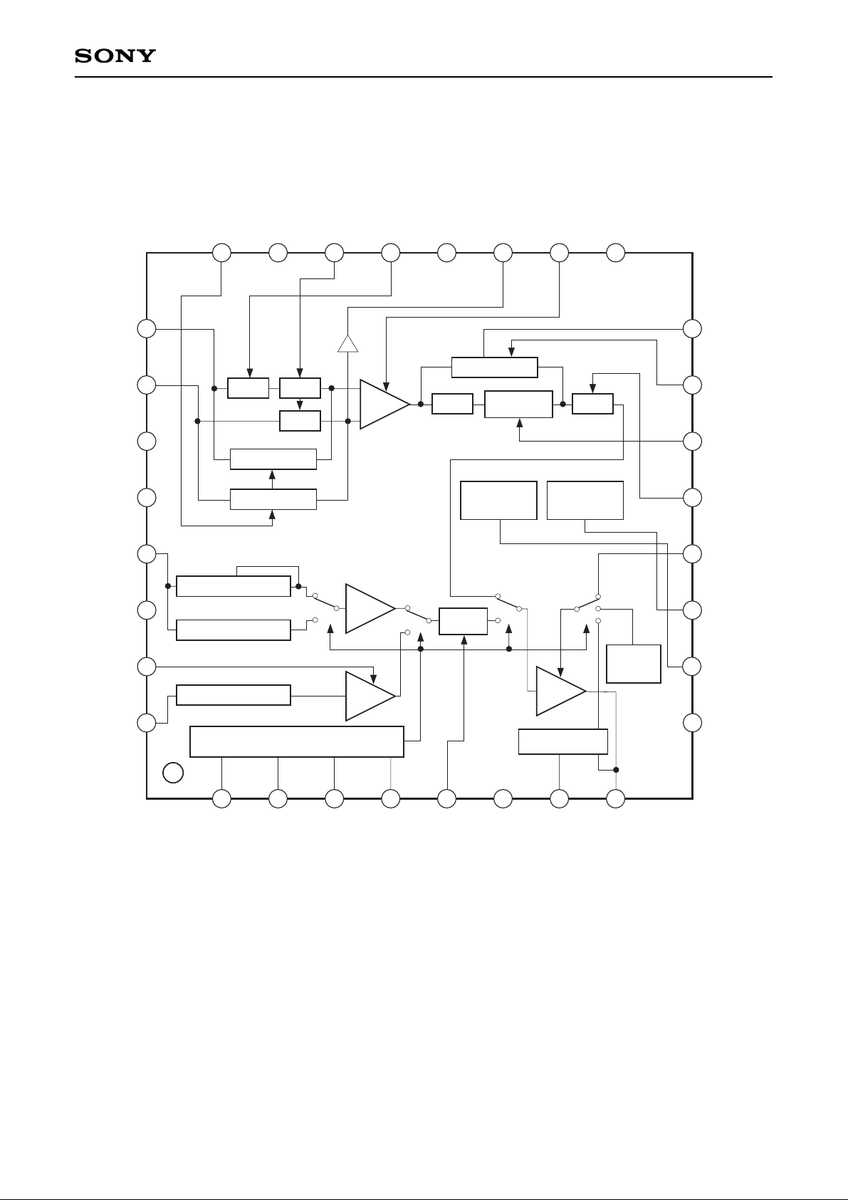
Block Diagram and Pin Configuration
CENTER BIAS
CENTER BIAS
LIN CLP
MODE SWITCHING
AMP
GCA
VISH
LOUTCLP
DRV
CH/CL
DC
AGC
COSCLP2
COSCLP1
SH3
SH2SH1
BLKLPF
AGCCLP
CAMSH
REF
BOTTOM
REF
TOP
CH/CL
GND3
LOUTCLP
DRVOUT
VSHP
PBLK
XRS
CLPOB
VRT
VRB
OFFSET
V
CC3
V
CC2
PIN
DIN
PBRFC
RFCONT
LIN/CH
CLPDM
GND1
SHD
SHP
V
CC
1
AGCCONT
CCDLEVEL
N.C.
AGCCLP
N.C.
GND2
9
10
11
12
13
14
15
16
17
18
19
20
21
22
23
24
25
26
27
28
29
30
31
32
2
3
4
5
6
7
8
1
CAM/VIDEO
PB/REC
PS
LIN/CH SW
VI SW
C/V SW
OFFSET
SW
– 3 –
CXA2006Q
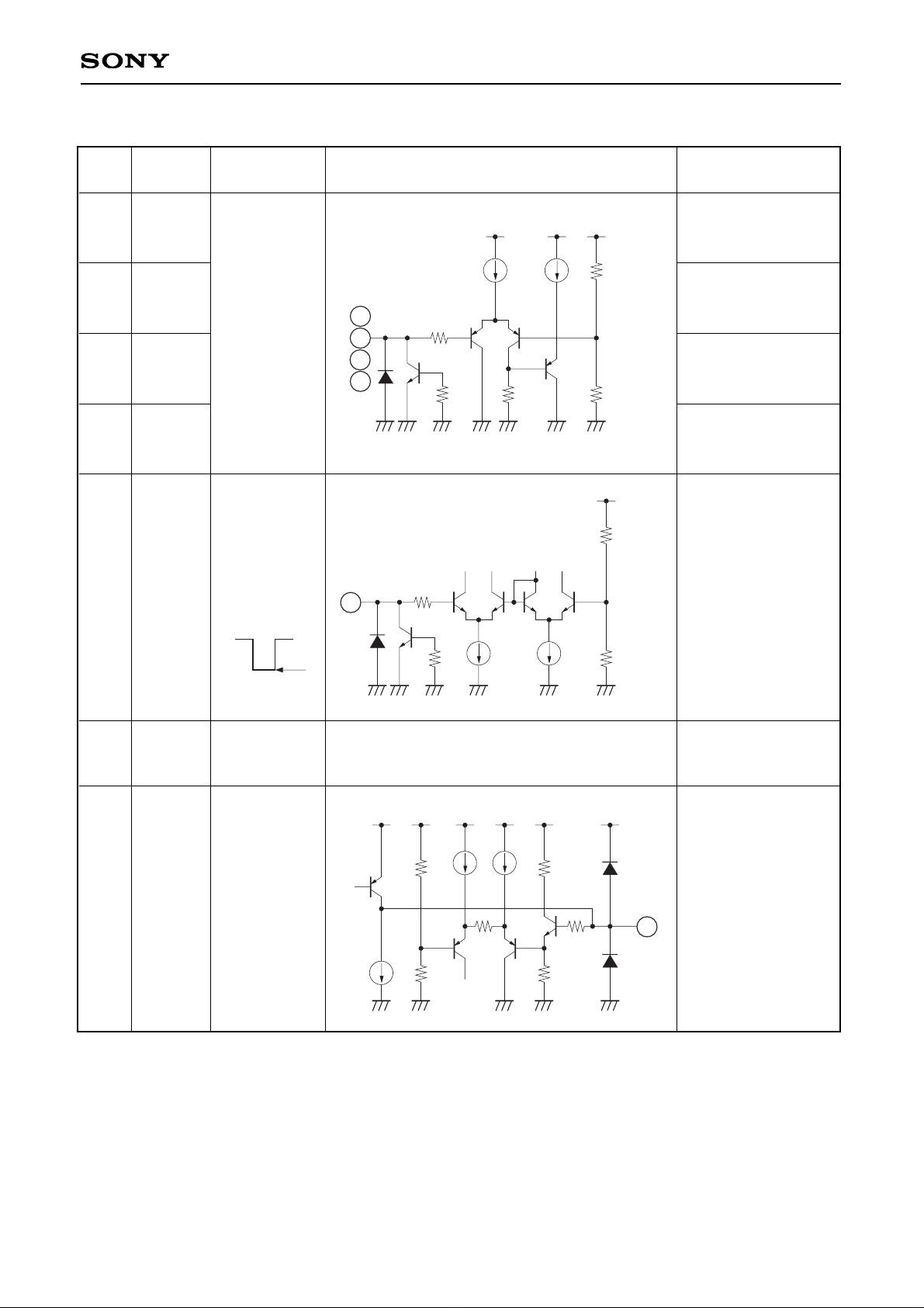
Pin Description (VCC1, 2, 3 = 4.75V)
Pin
No.
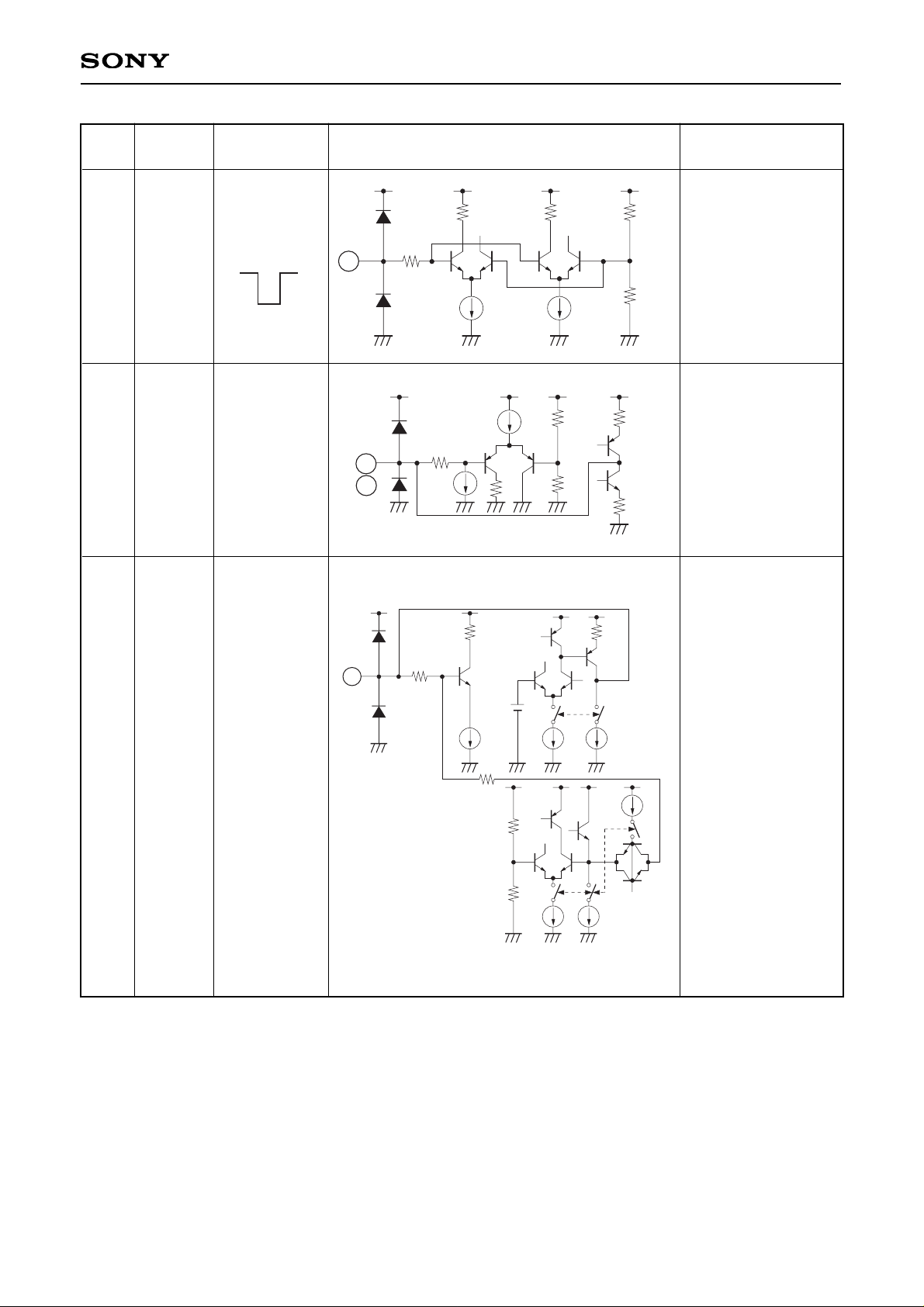
Symbol Pin voltage Equivalent circuit Description
1
CAM
/VIDEO
Camera and video
signal selector.
2 PB/REC
Chroma signal and
composite video
signal selector.
3 CH/CL
High-band chroma
signal and low-band
chroma signal selector.
4 PS Power save mode.
5 VSHP
Sample-and-hold
pulse input for video.
6
23
30
GND3
GND23
GND2
Ground.
7
LOUTCLP
Capacitor connection
for LOUTCLP which
clamps the output
minimum level in
modes which pass
the composite video
signal.
(Recommended
value: 0.1µF)
VTH = 1.35V
Sampling
VTH = 1.32V
GND
Approx. 2V
1.35V
127
10k 24k
27k
25µA 25µA
68k
2
3
4
1
127
10k
6.25k
2mA
16.25k
1.32V
400µA
5
127
24k
66k
200µA
100k
1.1k
100µA
1.27V
16k
4µA
7
Sampling
– 4 –
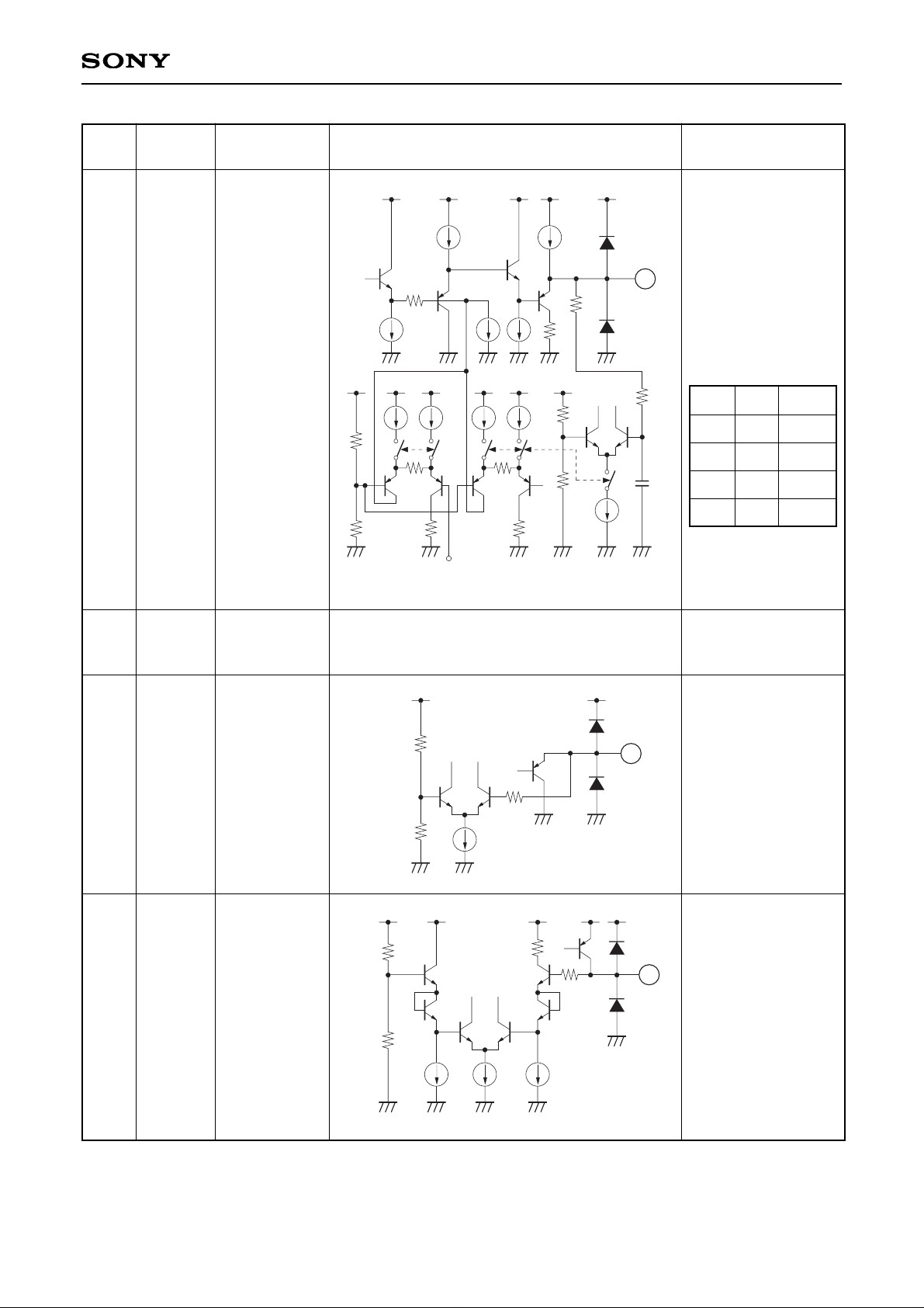
CXA2006Q
8
DRVOUT
Driver output for A/D
converter capable of
DC coupling.
Dynamic range
= 2Vp-p
• Camera mode
(CAM)
VRB – 200mV
< black level
<
VRB + 300mV
• Composite
video mode
(LIN)
VRB + 100mV
• Chroma mode
(CH, CL)
Center voltage =
(VRT – VRB)/2
10 VRB
2V regulator output.
Be sure to decouple
this pin near the IC
pins to prevent the
oscillation and external
noise when this pin is
not used.
(Recommended
capacitor value: 4.7µF)
9
20
27
VCC3
VCC1
VCC2
Power supply.VCC
2.0V
4.0V11 VRT
4V regulator output.
Be sure to decouple
this pin near the IC
pins to prevent the
oscillation and external
noise when this pin is
not used.
(Recommended
capacitor value: 4.7µF)
100µA
50
30k
127
4mA
1.5mA
1.5mA
DRVOUT
10p
OFFSET
2.1V
SW2SW1
8
SW1 SW2 Mode
0
0
1
1
0
1
0
1
CH, CL
CAM
LIN
—
0: Closed
1: Open
2V
10k
100µA
13.75k
2k
10
4V
20k
100µA
3.75k
3k
100µA
1.1k
100µA
11
Pin
No.
Symbol Pin voltage Equivalent circuit Description
– 5 –
CXA2006Q
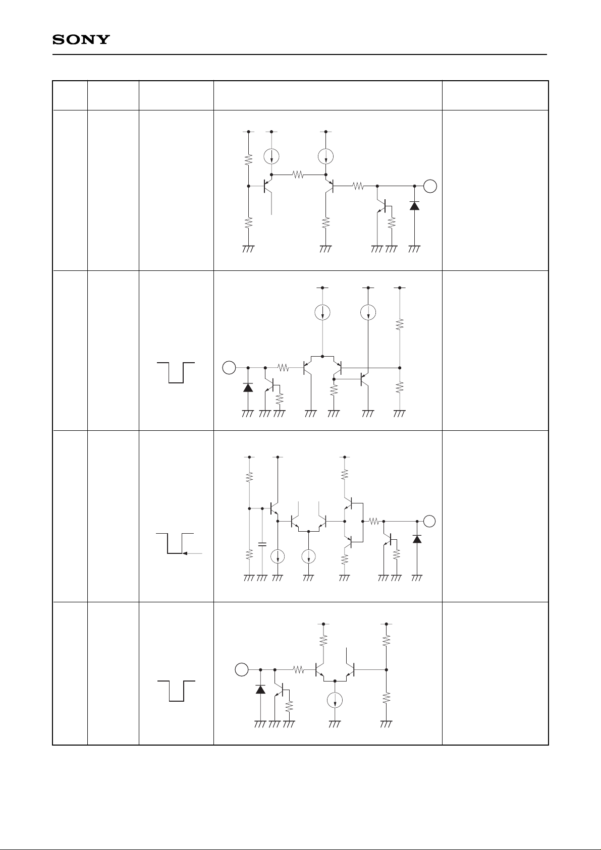
12 OFFSET
Controls the output
offset during camera
mode.
When 0V:
less than
(VRB – 200mV)
When 3.0V:
greater than
(VRB + 300mV)
0 to 3V
24k
100µA
66k
23k
1.1k
100µA
127
10k
12
13 PBLK
Camera signal preblanking pulse input.
Active when Low only
during camera mode.
Calibrates the black
level of the AGC
output waveform.
When PBLK is Low,
the DRVOUT
potential is forced to
2V.
VTH = 1.35V
27k
25µA
68k
24k
25µA
127
10k
1.35V
13
14 XRS
Camera signal
sample-and-hold
pulse input.
VTH = 2.16V
10.25k
12.25k
200
100µA
127
10k
200
2.5mA
2.16V
5p
14
15 CLPOB
Clamp pulse used to
clamp the optical
black portion of the
camera signal after it
passes through the
AGC amplifier.
VTH = 1.45V
29k
1.1k
127
10k
100µA
1.45V
66k
15
Active: Low
Sampling
Active: Low
Pin
No.
Symbol Pin voltage Equivalent circuit Description

– 6 –
CXA2006Q
16 AGCCLP
AGC clamp capacitor.
(Recommended
value: 0.1µF)
Approx. 3V
18
AGCCONT
AGC gain control.
When 0V: 8dB
(Minimum gain)
When 3.0V: 38dB
(Maximum gain)
0 to 3.0V
2k
2k
127
1.1k
50µA
16
127
10k
40µA
4k 20k 38k
40µA 20µA 20µA 20µA 20µA
20µA
18
19
CCDLEVEL
Enables monitoring
of the SHD output
camera signal.
DIN input
CCD signal
black level:
approx. 2.7V
21 SHP
Preset level sampleand-hold pulse input.
22 SHD
Data level sampleand-hold pulse input.
VTH = 2.38V
40µA
200
19
25k
25k
200
40µA
127
10k
200
670µA
2.38V
21
22
Sampling
Pin
No.
Symbol Pin voltage Equivalent circuit Description
– 7 –
CXA2006Q
24 CLPDM
Clamp pulse used to
clamp the dummy
pixel portion of the
input CCD signal.
VTH = 1.45V
29k
1.1k
85µA
127
1.45V
66k
1.1k
85µA
24
2526PIN
DIN
CCD signal input.
Black level:
approx. 2.7V
2k
2k
200
90µA
127
36k
14k
0.9µA
25
26
29
LIN/CH
Common input for
the composite video
signal (LIN) and
high-band chroma
signal (CH).
Clamp
potential
during LIN
mode:
approx. 2.4V
During CH
mode:
approx. 2.7V
26k
1k
200µA
127
100µA
2.7V
10k
2µA
2.1V
LIN mode
19k
100µA
CH mode
10k
29
Active: Low
Pin
No.
Symbol Pin voltage Equivalent circuit Description
 Loading...