

Sony CXA1999N Datasheet

—1—
E95517C8Y
Sony reserves the right to change products and specifications without prior notice. This information does not convey any license by
any implication or otherwise under any patents or other right. Application circuits shown, if any, are typical examples illustrating the
operation of the devices. Sony cannot assume responsibility for any problems arising out of the use of these circuits.
Absolute Maximum Ratings
• Supply voltage VCC 7.0 V
• Operating temperature Topr –20 to +75 °C
• Storage temperature Tstg –65 to +150 °C
• Allowable power dissipation PD 375 mW
Operating Condition
Supply voltage VCC1 1.1 to 4.0 V
Description
The CXA1999N is a low current consumption FM
IF amplifier which employs the newest bipolar
process. It is suitable for M-ary FSK pagers.
Features
• Low current consumption: 1.16 mA
(typ. at VCC = 1.4 V)
• Low voltage operation: VCC = 1.1 to 4.0 V
• Small package 20-pin SSOP
• Second mixer and oscillator
• Needless of IF decoupling capacitor
• Reference power supply for operational amplifier
and comparator
• IF input, VCC standard
Applications
• M-ary FSK pagers
• Double conversion pagers
Structure
• Bipolar silicon monolithic IC
IF Amplifier for M-ary FSK Pagers
20 pin SSOP (Plastic)
CXA1999N
—2—
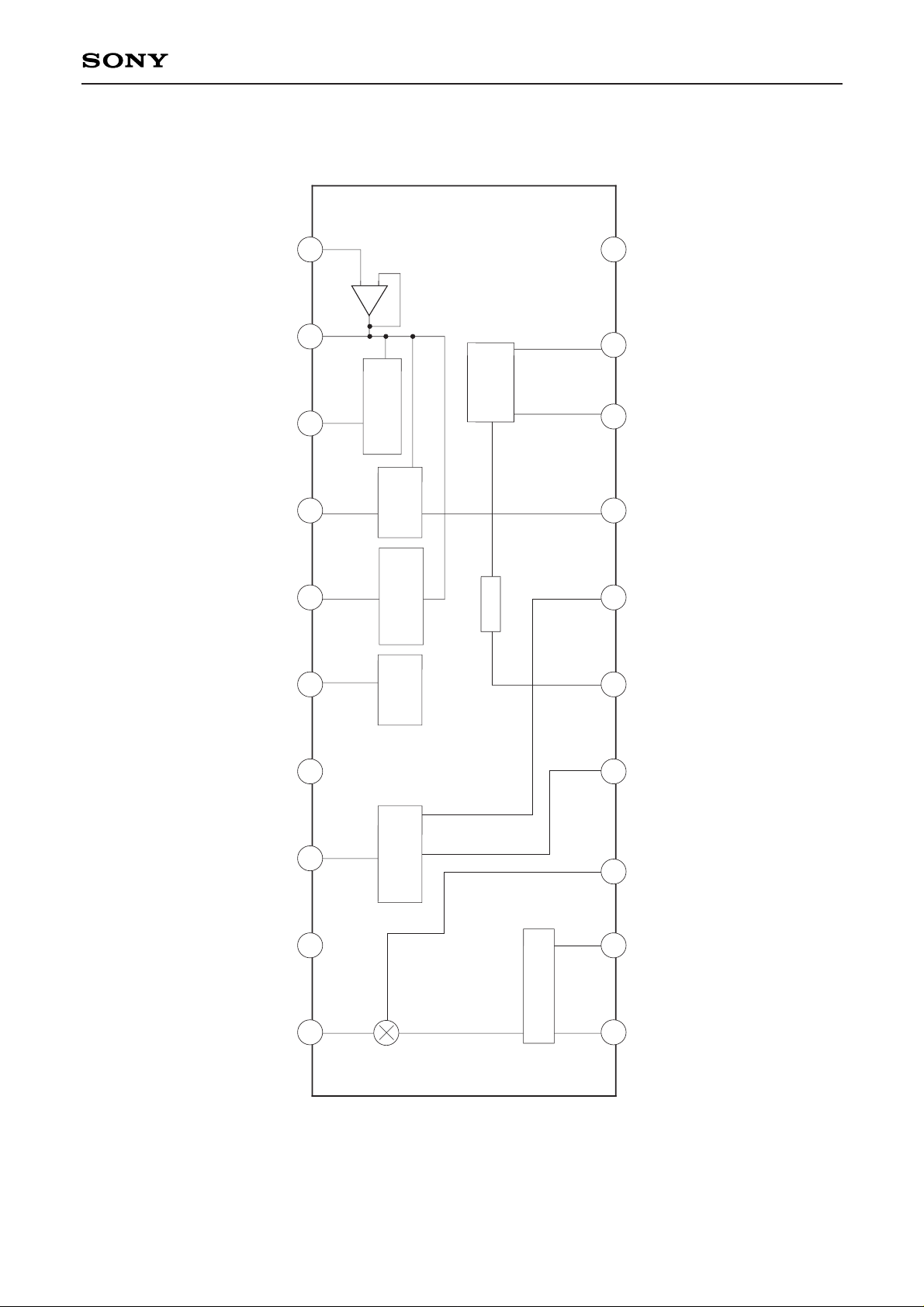
CXA1999N
1
2
3
4
5
6
7
8
9
10
OSC
IN
OSC
OUT
MIX
OUT
V
CC
IF IN B.S.
FSK
REF
QUAD
DET
OUT
RSSI
MIX
IN
11
12
13
14
15
16
17
18
19
20
GND
REG
OUT
REG
CONT
LVA
OUT
NRZ
OUT
CHARGE
L.C.
OUT
LPF OUT
LPF
IN
QUAD
DET
QUICK
CHARGE
IF LIM
MIXER
LOCAL
OSCILLATOR
REGULATOR
ALARM
NRZ
COMPARATOR
LEVEL
COMPARATOR
Block Diagram and Pin Configuration

—3—
CXA1999N
Pin Description
Pin
No.
Symbol Pin voltage Equivalent circuit Description
1
2
3
4
5
6
7
OSC IN
OSC OUT
MIX OUT
VCC
IF IN
B.S.
FSK REF
1.4 V
0.7 V
1.2 V
1.4 V
—
0.2 V
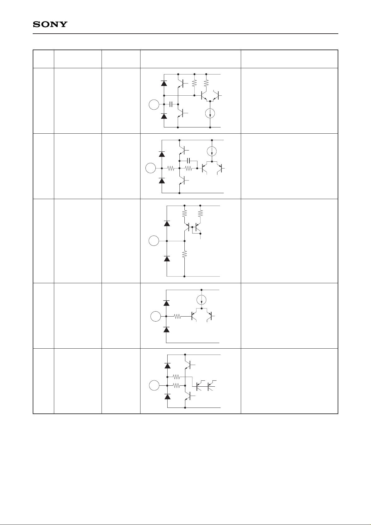
Connects the external parts of
crystal oscillator circuit.
A capacitor and crystal oscillator
are connected to these pins and
VCC.
Mixer output.
Connect a 455 kHz ceramic filter
between this pin and IF IN.
Power supply.
IF limiter amplifier input.
Controls the battery saving.
Setting this pin low suspends the
operation of IC.
(Applied voltage range: –0.5 V to
+7.0 V)
Connects the capacitor that
determines the low cut-off
frequency for the entire system.
2
1
VCC
300
15k
230
GND
72
15k
3
VCC
GND
1.5k
5
VCC
1.5k
GND
1.5k
8k 8k
6
72
40k
140k
GND
7
VCC
GND
72
—4—
CXA1999N
Pin
No.
Symbol Pin voltage Equivalent circuit Description
8
9
10
11
12
QUAD
DET OUT
RSSI
LPF IN
LPF OUT
1.4 V
0.2 V
0 V
0.2 V
0.2 V
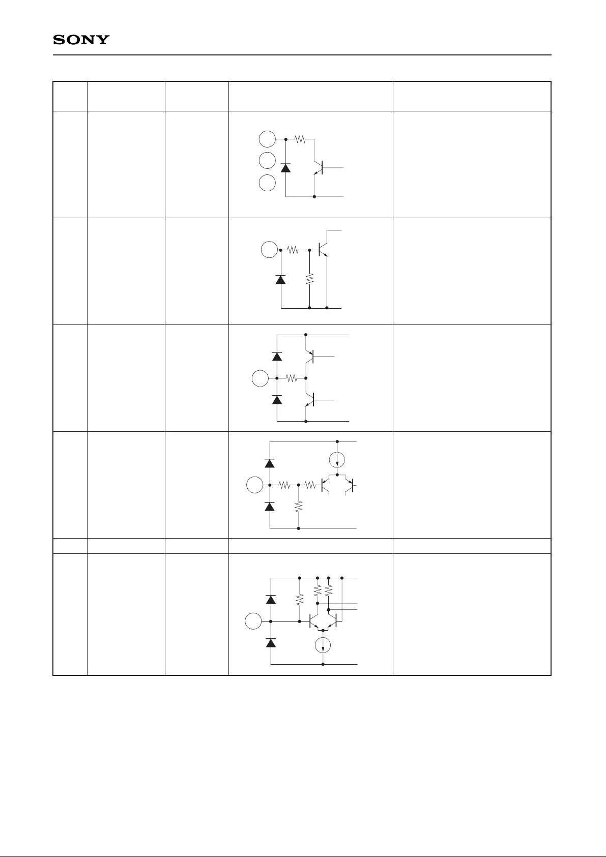
Connects the phase shifter of FM
detector circuit.
FM detector output.
RSSI circuit output.
Operational amplifier input.
Level comparator and NRZ
comparator inputs. Output for
operational amplifier is
connected.
8
VCC
22k
GND
20p
20k
9
VCC
GND
50p
55k
72
10
VCC
GND
7k 7k
70k
11
VCC
GND
72
12
VCC
GND
72
72
—5—
CXA1999N
Pin
No.
Symbol Pin voltage Equivalent circuit Description
13
15
16
14
17
18
19
20
L.C. OUT
NRZ OUT
LVA OUT
CHARGE
REG CONT
REG OUT
GND
MIX IN
—
—
—
0 V
—
1.0 V
—
1.4 V
Level comparator, NRZ
comparator and LVA comparator
outputs. They are open
collectors.
(Applied voltage range: –0.5 V to
+7.0 V)
Controls the ON/OFF operation
of the quick-charge circuit.
Set this pin high to execute the
quick charge.
(Applied voltage range: –0.5 V to
+7.0 V)
Output for internal constantvoltage source amplifier.
Connect the base of PNP
transistor.
(Current capacity: 100 µA)
Constant-voltage source output.
Controlled to maintain 1.0 V.
Ground
Mixer input.
14
20k
100k
GND
13
15
16
72
GND
17
VCC
GND
72
18
VCC
GND
78k
1k
22k
20
VCC
GND
2k
4.16k 4.16k

—6—
CXA1999N
Item
Current consumption
Current consumption
AM rejection ratio
Op amp. input bias current
Op amp. maximum output level
NRZ output saturation voltage
NRZ output leak current
NRZ hysteresis width
VB output current
VB output saturation voltage
REG OUT voltage
LVA operating voltage
LVA output leak current
LVA output saturation voltage
Detector output voltage
Logic input voltage high level
Logic input voltage low level
Limiting sensitivity
Level comparator output
saturation voltage
Level comparator output leak
current
RSSI output offset
Mixer input resistance
Mixer output resistance
IF limiter input resistance
Electrical Characteristics
Symbol
ICC
ICCS
AMRR
IBIAS
VO
VSATNRZ
ILNRZ
VTWNRZ
IOUT
VSATVB
VREG
VLVA
ILLVA
VSATLVA
VODET
VTHBSV
VTLBSV
VIN (LIM)
VSATLC
ILLC
VORSSI
RINLIM
ROUTMIX
RINLIM
Conditions
Measurement circuit 1
V2 = 1.0 V
Measurement circuit 1,
V2 = 0 V
Measurement circuit 3 30k LPF
Measurement circuit 2
Measurement circuit 4
Measurement circuit 6
Vin = 0.3 V
Measurement circuit 5
Vin = 0.1 V
Measurement circuit 5
Vin = 0.1 to 0.3 V
Measurement circuit 7
Measurement circuit 7
Output current 0 µA
Measurement circuit 8
V1 = 1.4 to 1.0 V
Measurement circuit 8 V1 = 1.0 V
Measurement circuit 9
Measurement circuit 3
—
—
Measurement circuit 3
Measurement circuit 11
Measurement circuit 10
Measurement circuit 12
—
—
—
Typ.
1.16
6
—
—
—
—
—
10
—
—
0.96
1.05
—
—
50
—
—
5
—
—
400
2.0
1.5
1.5
Max.
1.5
20
—
100
—
0.4
5.0
20
—
0.4
1.04
1.10
5.0
0.4
68
—
0.35
14
0.4
5.0
550
2.4
1.8
1.8
Unit
mA
µA
dB
nA
mVp-p
V
µA
mV
µA
V
V
V
µA
V
mVrms
V
V
dBµ
V
µA
mV
kΩ
kΩ
kΩ
Min.
0.8
—
25
—
160
—
—
—
100
—
0.89
1.00
—
—
38
0.9
—
—
—
—
—
1.6
1.2
1.2
(VCC = 1.4 V, Ta = 25 °C, Fs = 21.7 MHz, FMOD = 1.6 kHz, FDEV = 4.8 kHz, AMMOD= 30 %)
 Loading...