

Sony CXA1998BQ Datasheet

Description
The CXA1998BQ is an IC developed for analog
signal processing in tape recorders. Processing for
both the recording and playback systems is
achieved on one chip.
Features
• 11-bit serial data interface
• Recording/playback mute function
• Recording equalizer Gp and Fp can be adjusted
externally.
• AGC (Automatic Gain Control)
• Comparator for AMS (Automatic Music Sensor)
• Recording/playback equalizer amplifier with 1.7
times speed switching
Absolute Maximum Ratings (Ta = 25°C)
• Supply voltage VCC, VDD 12 V
• Operating temperature Topr –20 to +75 °C
• Storage temperature Tstg –65 to +150 °C
• Allowable power dissipation
PD 645 mW
Operating Conditions
Supply voltage VCC 6.5 to 10.0 V
VDD 4.5 to 5.5 V
Structure
Bipolar silicon monolithic IC
Applications
All analog signal processing in the cassette decks
of tape recorders and compact music centers
Applicable Head
Applicable to MITSUMI ELECTRIC Co., Ltd.
Playback head: BP-7442-CP-6973
Recording/playback head: BC-9242-CB-9267
– 1 –
CXA1998BQ
E98Z31-PS
Recording/Playback Equalizer Amplifier
Sony reserves the right to change products and specifications without prior notice. This information does not convey any license by
any implication or otherwise under any patents or other right. Application circuits shown, if any, are typical examples illustrating the
operation of the devices. Sony cannot assume responsibility for any problems arising out of the use of these circuits.
48 pin QFP (Plastic)
– 2 –
CXA1998BQ
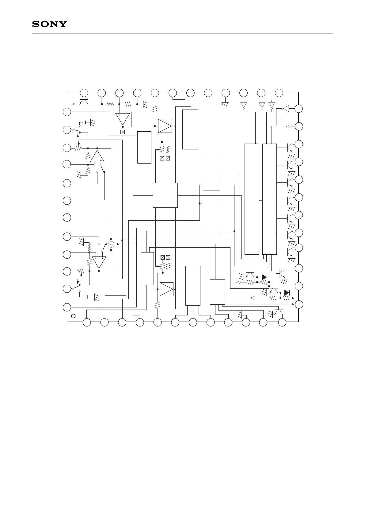
Block Diagram and Pin Configuration (Top View)
D1
D2
D3
D4
D5
D6
2
3
4
5
6
7
8
9
10
11
12
13
14
15
16
17
18
19
20
21
22
23
24
25
26
27
28
29
30
31
32
1
37
38
39
40
41
42
43
44
45
46
47
48
MUTE
AGC GAIN 19.5dB
10k
40k
RECEQ
AMS
GND
GND
GND
V
DD
VDD
20k 20k
20k20k
D11
D9
D10
D8
GND
D7
GND
D11
GND
D9
GND
GND
GND
GND
GND
GND
VDD
GND
40k
AGC GAIN 19.5dB
10k
RECEQ
IREF
36
35
34
33
GND
RFS
2.8V
210k
GND
GND
210k
GND
210k
210k
GND
2.8V
AGC
AGC OFF
A EQ
B EQ
PBEQ CTLRECEQ CTL
DECK A/B
SPEED
SHIFT REGISTERS
LATCHES
GP CAL
A EQ
B EQ
AGC TC
AGC IN1
REC IN1
AGC OUT1
REC OUT1
AMS GAIN
AMS GND
AMS TC
AMS OUT
PBMUTE
RMUTEI
RMUTE
SPEED
BPA
BPB
PL1
PL2
M1
M2
V
DD
LATCH
RFC
Vcc
VG
GND
AGC IN2
REC IN2
AGC OUT2
REC OUT2
DGND
XRESET
DATA
CLK
FP CAL
PB OUT1
PB FB21
PB FB11
PB INB1
PB INA1
PB INA2
PB INB2
PB FB12
PB FB22
PB OUT2
IREF

– 3 –
CXA1998BQ
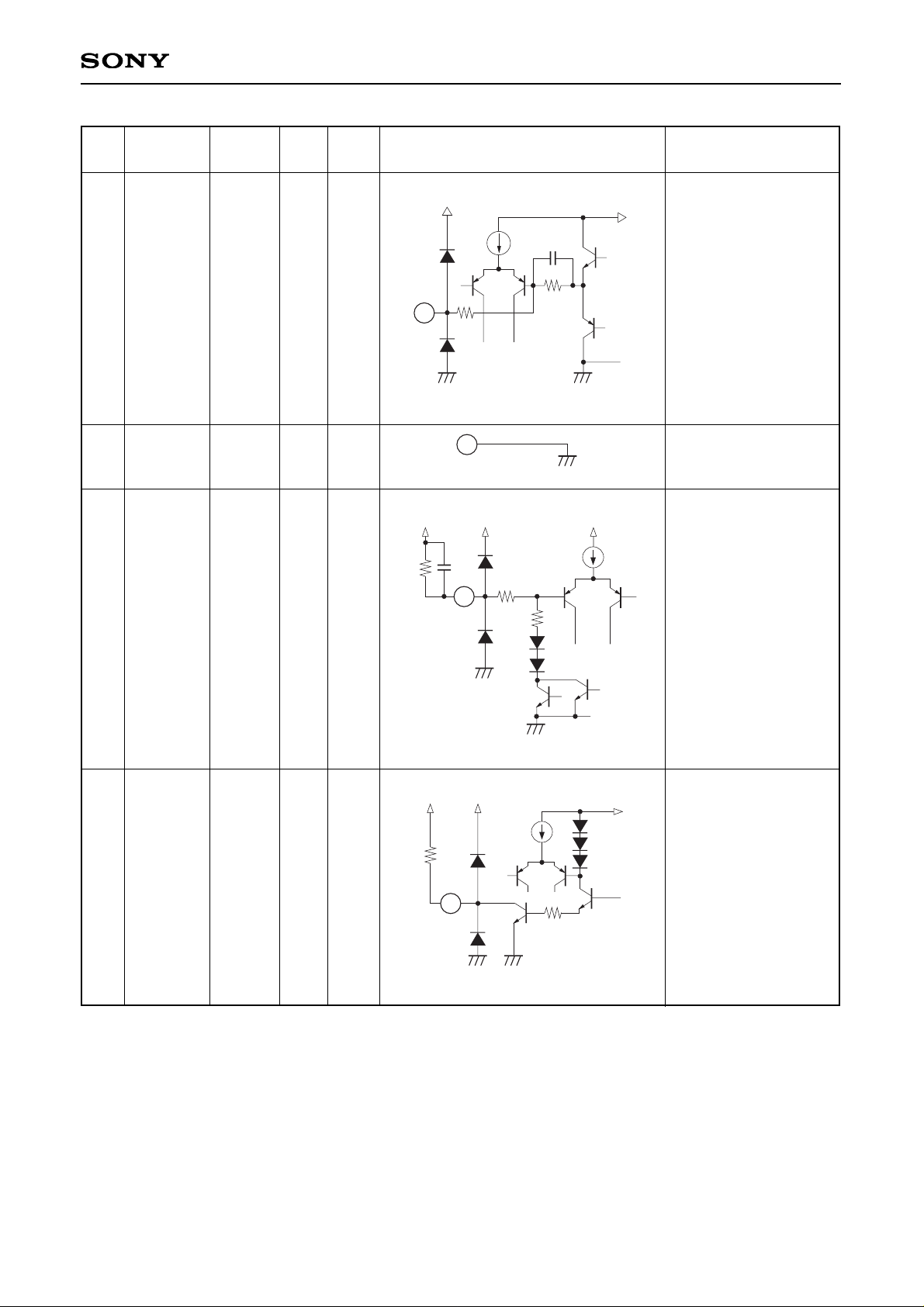
Pin Description
Pin
No.
1
Symbol
DC
voltage
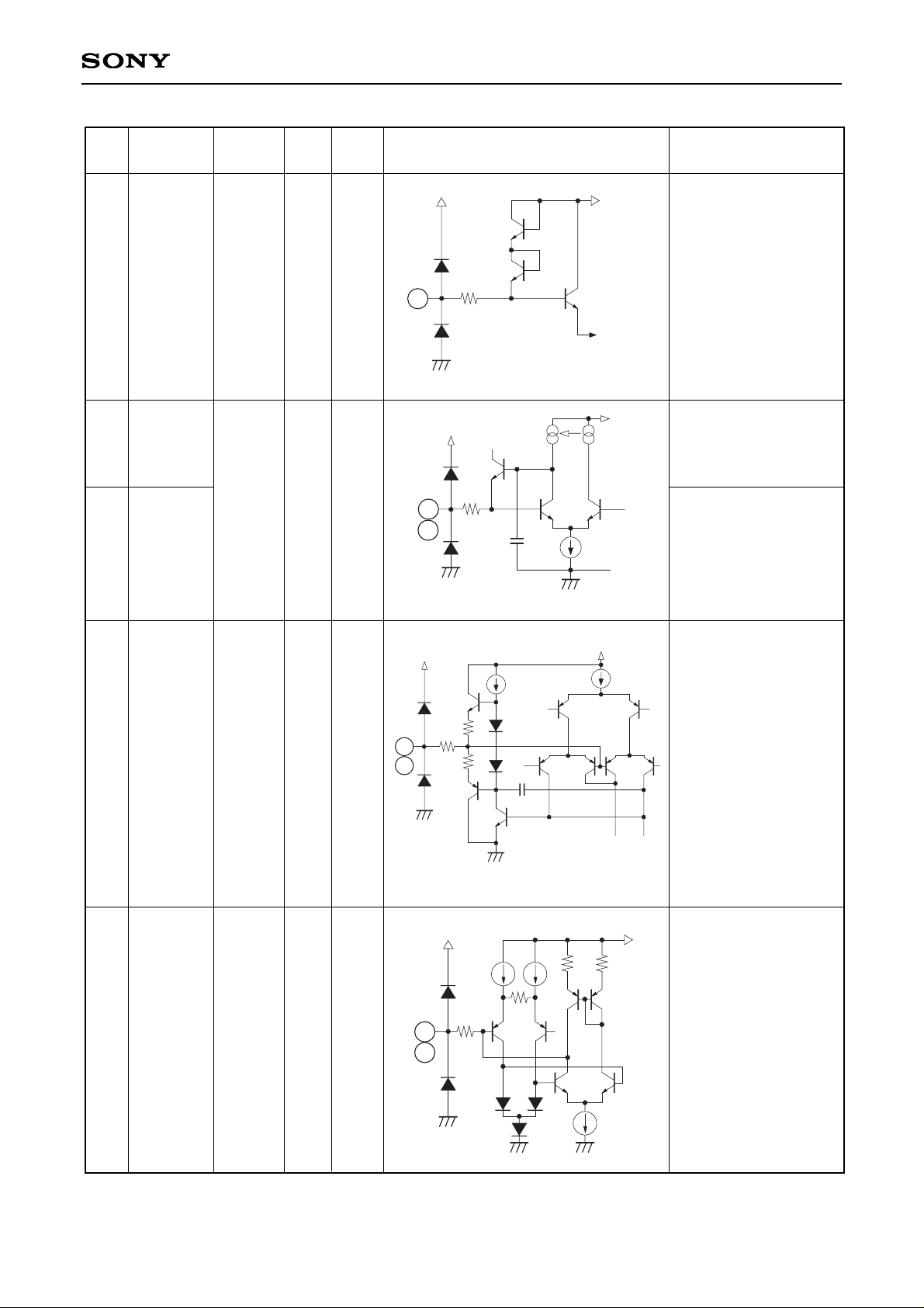
I/O Equivalent circuit Description
GP CAL
1.2V —
Connects a resistor
for determining the
high-band peak gain
of recording equalizer.
Reference setting
resistance is 27kΩ.
I/O
resistance
—
2
A EQ
— I
Deck A equalizer
switch.
Low: 120µs EQ
High: 70µs EQ
—
3
B EQ
2.5V
(OPEN)
I
Deck B equalizer
switch.
Low: NORMAL TAPE,
120µs EQ
Medium: Cro2 TAPE,
70µs EQ
High: METAL TAPE,
70µs EQ
53kΩ
4
AGC TC
0.0V
—
Connects a resistor
and capacitor for
determining AGC
attack/recovery time
constants.
—
1
Vcc
Vcc
GND GND
147
× 2
30k
VCC
147
GND
GND
VCC
2
VCC
147 50k
V
CC
GND
GND
5k
5k
3
VCC
GND
GND
VCC
× 2
200
100k
500
500
× 2
147
× 2
× 4
200
5k
4
(Ta = 25°C, VCC = 8V, VDD = 5V, no signal, RESET ON)

– 4 –
CXA1998BQ
5
32
AGC IN1
AGC IN2
4.0V I
AGC signal input.
Input resistance
changes between
50kΩ and 100kΩ.
AGC functions when
the signal of –30dBm
or more is input to
AGC for AGC ON.
(External 47µF//300kΩ
for Pin 4)
50kΩ
6
31
REC IN1
REC IN2
4.0V I
Recording equalizer
input.
50kΩ
7
30
AGC OUT1
AGC OUT2
4.0V O AGC output.147Ω
8
29
REC OUT1
REC OUT2
4.0V O
Recording equalizer
output.
147Ω
VCC
147
40k
500
× 10
V
CC
GND
GND
× 3
500
× 2
5p
8
29
VCC
147
18752
500
× 4
V
CC
GND
VGS
GND
× 2
500
7
30
107423
9945
VGS
VCC
147
50k
V
CC
GND
VGS
23186
1759
VGS
GND
6
31
VCC
147 10k
40k
× 4
V
CC
GND
VGS
5
32
Pin
No.
Symbol
DC
voltage
I/O Equivalent circuit Description
I/O
resistance
– 5 –
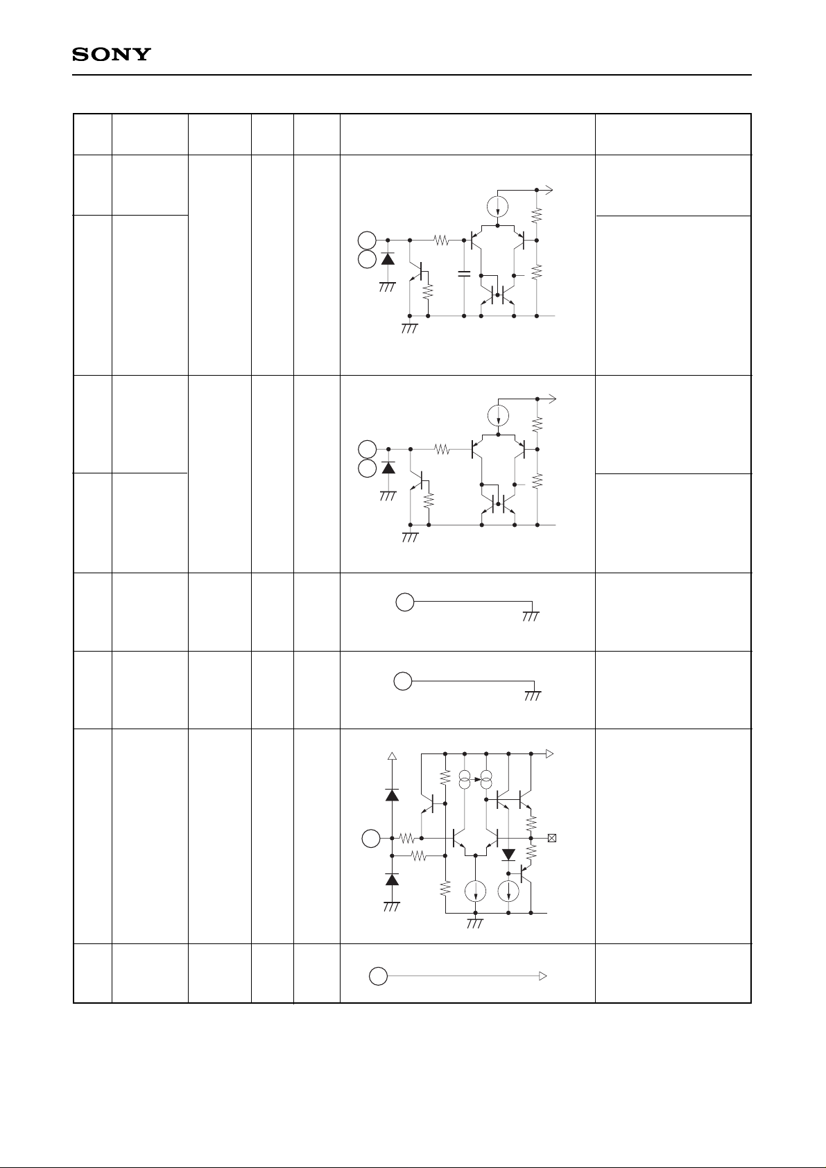
CXA1998BQ
AMS block ground.
9
AMS GAIN
3.5V —
Connects a resistor
for determining AMS
signal detection level
and a capacitor for
determining HPF cutoff frequency.
—
10
AMS GND
0.0V
— —
12
AMS OUT
8.0V
O
AMS output.
No signal detection:
High
Signal detection: Low
—
11
AMS TC
8.0V —
Connects time
constant for AMS
detection.
—
VCC
147
GND
VCC
GND
100k
10µ
9
11
Vcc
GND
1k
GND
147
VccVcc
GND
Vcc
12
Vcc
Vcc
10k
GND
10
GND
Pin
No.
Symbol
DC
voltage
I/O Equivalent circuit Description
I/O
resistance
– 6 –
CXA1998BQ
13
PBMUTE
14
RMUTE1
5.0V —
Connects a capacitor
for setting time
constant for playback
mute ON/OFF
switching.
—
15
RMUTE
Output for recording
mute ON/OFF switch
control signal. Outputs
D11 from Pin 26
(DATA).
16
SPEED
5.0V
O
Output for
recording/playback
equalizer speed switch
control signal. Outputs
D9 from Pin 26 (DATA).
Low: Normal Speed
High: High Speed
(1.7 times)
—
17
BPA
5.0V O
Outputs D6 from
Pin 26 (DATA).
18
BPB
Outputs D5 from
Pin 26 (DATA).
19
PL1
Outputs D4 from
Pin 26 (DATA).
20
PL2
Outputs D3 from
Pin 26 (DATA).
21
M1
Outputs D2 from
Pin 26 (DATA).
22
M2
Outputs D1 from
Pin 26 (DATA).
23
VDD
Power supply of serial
data interface block.
—
5.0V
—
—
13
14
VDD
VDD
20k
20k
GND
× 4
147
GND
GND
Connects a capacitor
for setting time
constant for recording
mute ON/OFF
switching.
× 4
VDD
5k
GND
GND
VDD
× 4
5k
20k
15
16
× 4
VDD
GND
GND
VDD
× 4
10k
20k
17
18
19
20
21
22
VDD
23
Pin
No.
Symbol
DC
voltage
I/O Equivalent circuit Description
I/O
resistance
– 7 –
CXA1998BQ
24
LATCH
27
XRESET
— I
Serial data interface
latch input.
—
25
DATA
—
I
Serial data interface
reset input.
Low: Reset.
At this time serial
data outputs
(Pins 15 to 22)
are all open
(high).
—
26
Serial data interface
clock input.
Serial data interface
serial data input.
28
DGND
0.0V
—
Serial data interface
block ground.
—
CLK
2k
GND
VDD
10.5k
25µA
GND
30k
5p
× 4
30k
24
27
4k
GND
VDD
10.5k
25µA
GND
30k
× 4
30k
25
26
GND
28
33
GND
0.0V
—
Ground.
—
35
VCC
8.0V — Power supply.—
34
VG
4.0V —
Signal reference
voltage. Connects a
capacitor for ripple
rejection.
60kΩ
GND
33
34
VCC
147
45k
30k
× 4
V
CC
GND
GND
500
500
× 2
30k
× 2
To each VGS
35
VCC
Pin
No.
Symbol
DC
voltage
I/O Equivalent circuit Description
I/O
resistance
– 8 –
CXA1998BQ
Connects a resistor
(12kΩ) for determining
equalizer gains.
36
RFC
8.0V —
Connects a resistor
and capacitor for
obtaining stable
voltage with power
supply ripple rejected.
—
37
IREF
38
47
PB OUT2
PB OUT1
2.8V O
Playback equalizer
output.
147Ω
48 FP CAL
1.2V —
Connects a resistor for
determining the highband peak frequency
of recording equalizer.
Reference setting
resistance is 27kΩ.
—
36
VCC
147
V
CC
GND
× 3
× 250
× 3
To each RFS
Vcc
GND
× 2
GND
37
48
147
5p
Vcc
Vcc
GND
Vcc
× 3
500
147
× 6
GND
15p
47
38
500
39
46
PB FB22
PB FB21
2.8V —
Connects a capacitor
for determining
playback equalizer
time constants, such
as 120µs and 70µs.
—
39
46
VCC
147
× 3
GND
2k2k
GND GND
× 4
7k
× 3
× 4
RFS
Pin
No.
Symbol
DC
voltage
I/O Equivalent circuit Description
I/O
resistance

– 9 –
CXA1998BQ
40
45
PB FB12
PB FB11
1.4V —
Playback equalizer
negative feedback.
105kΩ
41
42
43
44
PB INB2
PB INA2
PB INA1
PB INB1
0.0V I
Playback equalizer
input.
70kΩ
41
42
43
44
45
70k
10p
VCC
GND
VCC
GND
× 6
VCC
40
GND
1k
1k
210k
210k
VCC
RFS
× 2
10k
5k
× 6
147
30p
147
Note)
• AMS GND (Pin 10), DGND (Pin 28) and GND (Pin 33) are each independent in the IC and are not connected.
Be sure tp ground each of the ground pins listed above.
• The resistance of open collector outputs (Pins 15 to 22) can be connected Vcc.
Pin
No.
Symbol
DC
voltage
I/O Equivalent circuit Description
I/O
resistance
 Loading...