

Sony CXA1994BM, CXA1994AM Datasheet

M-ary FSK Demodulating Comparator
Description
The CXA1994AM/BM is a comparator which allows
the M-ary (4-level) FSK data to be demodulated in
combination with an FM IF amplifier for pagers.
Features
• Low power consumption
70µA (at VCC = 1.4V, including the current on
battery saving control pin)
• Low voltage operation
VCC = 1.0 to 4.0V
Applications
M-ary FSK pagers
Function
• Window comparator for MSB detection
• Battery saving control pin
• Threshold level adjustment pin
Absolute Maximum Ratings (Ta = 25°C)
• Supply voltage VCC 7.0 V
• Operating temperature Topr –20 to +75 °C
• Storage temperature Tstg –65 to +150 °C
Operating Conditions
• Supply voltage VCC 1.0 to 4.0 V
– 1 –
E96428A8Y
Sony reserves the right to change products and specifications without prior notice. This information does not convey any license by
any implication or otherwise under any patents or other right. Application circuits shown, if any, are typical examples illustrating the
operation of the devices. Sony cannot assume responsibility for any problems arising out of the use of these circuits.
CXA1994AM/BM
8 pin SOP (Plastic)
Block Diagram
B.S.
GND
NC
DATA OUT
V
CC
DATA IN
REF
TH CONT
2
3
4
5
6
7
8
1
For the availability of this product, please contact the sales office.
– 2 –
CXA1994AM/BM
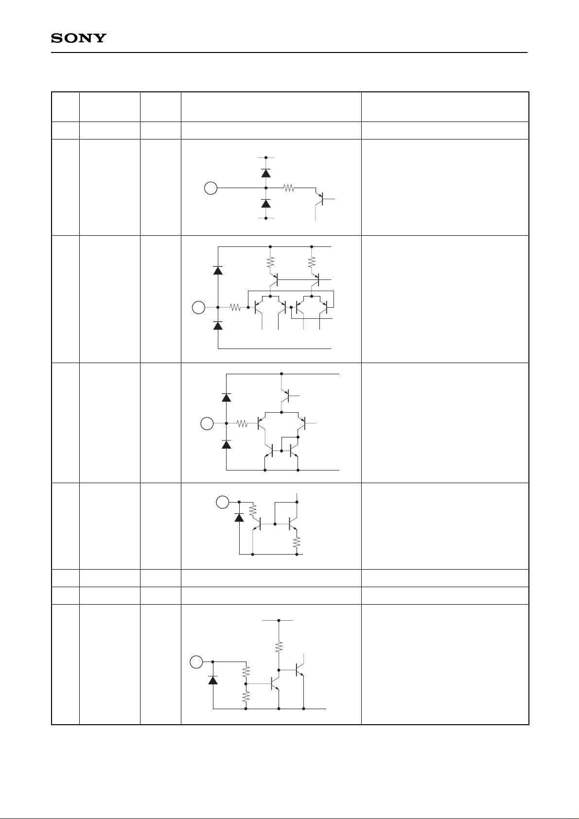
Pin Description
Pin
No.
Symbol
Pin
voltage
Equivalent circuit Description
1 VCC 1.5V Vcc.
2 TH CONT —
Adjusts the threshold level for
comparator.
3 DATA IN 0.2V
Signal input.
Connected to the COMP IN pin of
the CXA1484A.
4
REF 0.2V
Reference input.
Connected to the SENSE pin of the
CXA1484A.
5 DATA OUT —
Comparator output.
8
B.S.
—
Battery saving control.
6 NC —
7 GND 0 Ground.
VCC
GND
2
VCC
GND
3
4
GND
5
VCC
GND
8

– 3 –
CXA1994AM/BM
µA
µA
mV
mV
V
V
V
Electrical Characteristics (VCC = 1.4V, Ta = 25°C)
Item Symbol Condition Min. Typ. Max. Unit
Current consumption
Current consumption
Comparator input voltage high level
Comparator input voltage low level
Comparator output saturation voltage
Logic input voltage high level
Logic input voltage low level
ICC
ICCS
VCOMPH
VCOMPL
Vsat
VTHH
VTHL
VREF as a reference
VREF as a reference
0.9
70
50
–50
100
6
0.4
0.35
Pin Description
1. VCC Power supply pin of 1V or more
2. TH CONT This pin adjusts the threshold level and the default is approximately ±50mV from the
reference voltage. The threshold level can be set lower by inserting a resistor between VCC
and this pin. (The level cannot be set higher.)
3. DATA IN The signal after passing through the data filter of the IF IC (CXA1484A) is input.
4. REF Connects to the reference voltage pin of the IF IC. (Pin 15 of the CXA1484A)
5. DATA OUT Comparator output.
6. NC Not connected.
7. GND Ground.
8. B.S. Battery saving control pin. Battery saving state for low; normal operation for high.
 Loading...