

Sony CXA1982Q Datasheet

CXA1982Q
For the availability of this product, please contact the sales office.
RF Signal Processing Servo Amplifier for CD players
Description
The CXA1982Q is a bipolar IC with built-in RF
signal processing and various servo ICs. A CD
player servo can be configured by using this IC, DSP
and driver.
Features
• Low operating voltage (VCC – VEE = 2.8 to 4.0V)
• Low power consumption (36mW, VCC = 3.0V)
• Supports pickup of either current output, voltage
output
• Supports tracking system balance adjustment
externally
• Single power supply and positive/negative dual
power supplies
Absolute Maximum Ratings (Ta = 25°C)
• Supply voltage VCC 12 V
• Operating temperature Topr –20 to +75 °C
• Storage temperature Tstg –65 to +150 °C
• Allowable power dissipation
48 pin QFP (Plastic)
PD 833 mW
Applications
• RF I-V amplifier, RF amplifier
• Focus and tracking error amplifier
• APC circuit
• Mirror detection circuit
• Defect detection and prevention circuits
• Focus servo control
• Tracking servo control
• Sled servo control
Structure
Bipolar silicon monolithic IC
Recommended Operating Condition
Operating supply voltage
VCC – VEE 2.8 to 4.0 V
Sony reserves the right to change products and specifications without prior notice. This information does not convey any license by
any implication or otherwise under any patents or other right. Application circuits shown, if any, are typical examples illustrating the
operation of the devices. Sony cannot assume responsibility for any problems arising out of the use of these circuits.
– 1 –
E97215-PS
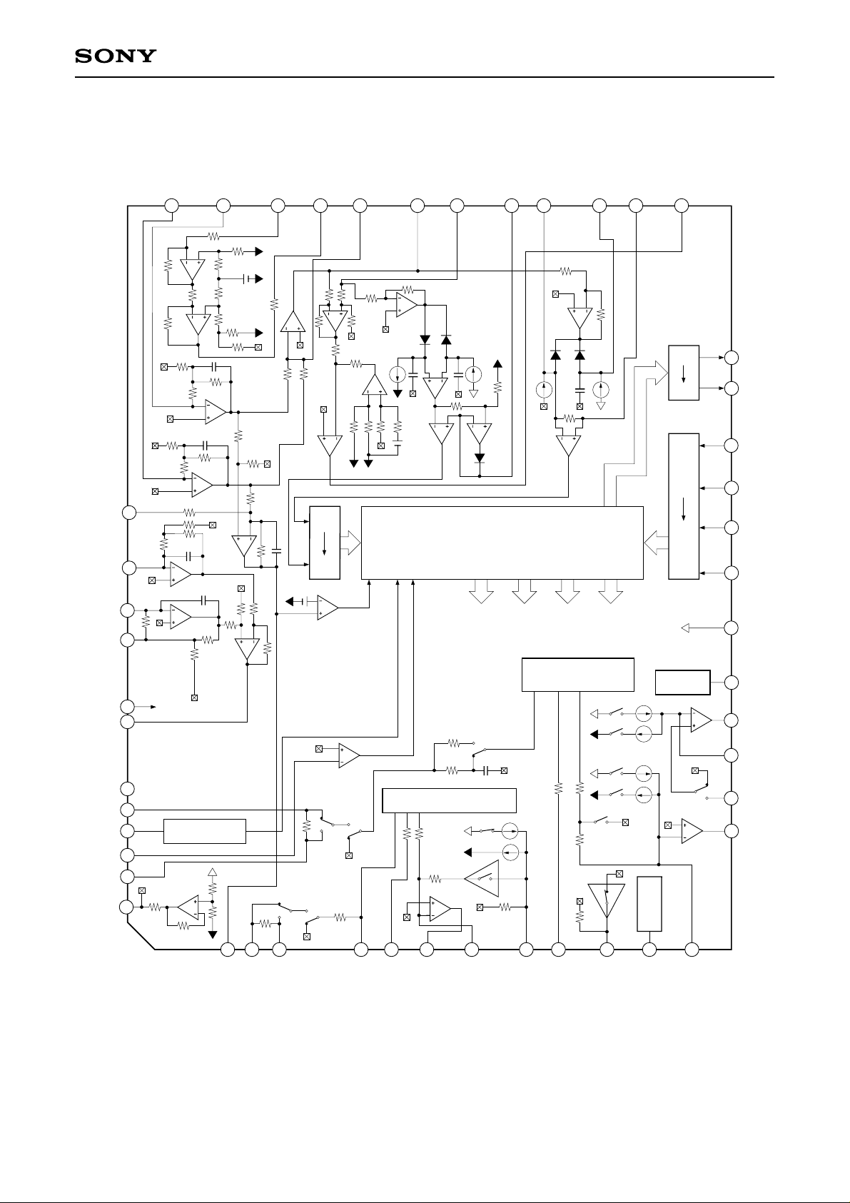
Block Diagram
CXA1982Q
FE_BIAS
V
TEO
NC
TEI
ATSC
TZC
TDFCT
VC
CB
CP
29
DFCT
•OUTPUT DECODER
•TRACKING
PHASE COMPENSATION
TG2
TM7
34
DFCT
PD
LD
33
FOK
TTL
I IL
TZC COMP
DFCT
FS4
32
LEVEL S
FZC COMP
TM1
RF_M
RF_O
31
MIRR
•I IL DATA REGISTER •INPUT SHIFT REGISTER
•ADRESS.DECODER
•FCS PHASE COMPENSATION
RF_I
30
FS1 to 4 TG1 to 2 TM1 to 7 PS1 to 4
TG1
FS1
FS2
PHD2
36
RF IV AMP2
37
F
38
F IV AMP
39
E
EI
40
EE
41
42
43
44
45
46
47
48
E IV AMP
•WINDOW COMP.
PHD1
35
APC
RF IV AMP1
FE AMP
TE AMP
ATSC
CC1
TM6
TM5
TM4
TM3
CC2
262728
•F SET
25
I IL
TTL
TTL
I IL
•I SET
FOK
TM2
SENS
24
23
C.OUT
XRST
22
21
DATA
20
XLT
CLK
19
18
Vcc
17
ISET
SL_O
16
SL_M
15
14
SL_P
13
TA_O
1
FEO
2
3
FEI
FDFCT
4
FGD
FLB
FE_O
7
FE_M
8
SRCH
9
6
5
TGU
10
11
12
TG2
FSET
TA_M
• The switch state in Block Diagram is for initial resetting.
• Switch turns to side for 1 and to side for 0 in Serial Data Truth Table.
• DFCT switch turns to side when defect signal generates for DEFECT = E in Serial Data Truth Table.
• TG1 switch turns to side and TG2 switch is left open when TG1 and TG2 (address 1 : D3) is 1.
°
°
°
•
– 2 –
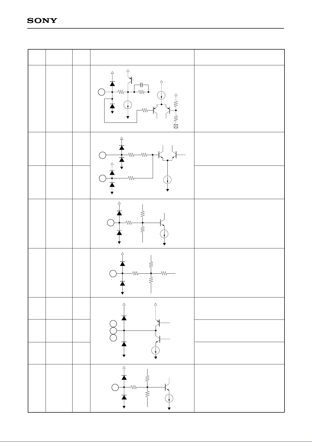
Pin Description
CXA1982Q
Pin
No.
1 FEO
2
FEI
FDFCT
3
Symbol
I/O
O
Equivalent circuit
25p
1
I
I
3
147
174k
51k
300µ
2
147
147
10k
100k
9k
Focus error amplifier output.
Connected internally to the FZC
comparator input.
Focus error input.
Capacitor connection pin for defect
time constant.
Description
4
5
6
13
16
FGD
FLB
FE_O
TA_O
SL_O
40k
68k
130k
20µ
147
I
I
4
5
Ground this pin through a capacitor
when decreasing the focus servo
high-frequency gain.
External time constant setting pin
for increasing the focus servo lowfrequency.
O
6
O
O
13
16
250µ
Focus drive output.
Tracking drive output.
Sled drive output.
FE_M
7
I
7
147
90k
Focus amplifier inverted input.
50k
– 3 –

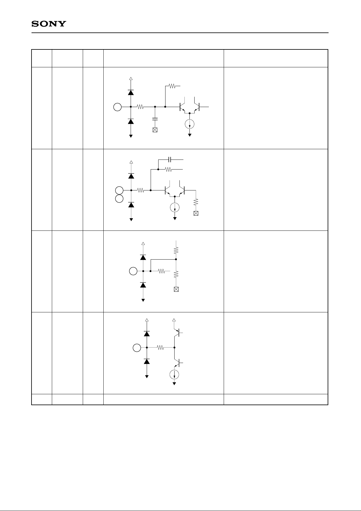
CXA1982Q
Pin
No.
8
9
10
Symbol
SRCH
TGU
TG2
I/O
I
Equivalent circuit
147
I
I
8
50k
110k
20k
9
11µ
External time constant setting pin for
generating focus servo waveform.
External time constant setting pin for
switching tracking high-frequency
Description
gain.
82k
External time constant setting pin for
10
470k
2µ
switching tracking high-frequency
gain.
11
12
14
FSET
TA_M
SL_P
I
11
147k
High cut-off frequency setting pin for
focus and tracking phase
compensation amplifier.
15k 15k
147
100k
Tracking amplifier inverted input.
11µ
Sled amplifier non-inverted input.
I
12
I
147
14
15
SL_M
I
15
147
22µ
Sled amplifier inverted input.
– 4 –

CXA1982Q
Pin
No.
17
Symbol
ISET
19 CLK
20
XLT
DATA
21
XRST
22
C. OUT
23
SENS
24
I/O
O
O
Equivalent circuit
I
17
147
I
15µ
I
I
19
20
21
22
147
1k
I
Setting pin for Focus search, Track
jump, and Sled kick current.
Serial data transfer clock input from
CPU. (no pull-up resistance)
Latch input from CPU.
(no pull-up resistance)
Serial data input from CPU.
(no pull-up resistance)
Reset input; resets at Low.
(no pull-up resistance)
Description
Track number count signal output.
20k
23
24
147
100k
Outputs FZC, DFCT, TZC, gain,
balance, and others according to
the command from CPU.
25
26
27
28
FOK
CC2
CC1
CB
20k
O
25
147
I
147 147
28
O
I
40k
100k
147
Focus OK comparator output.
Input for the DEFECT bottom hold
output with capacitance coupled.
27
DEFECT bottom hold output.
26
Connection pin for DEFECT bottom
hold capacitor.
– 5 –

CXA1982Q
Pin
No.
29
30
31
32
Symbol
I/O
CP
RF_I
RF_O O
RF_M
Equivalent circuit
147
29
I
Connection pin for MIRR hold
capacitor.
MIRR comparator non-inverted
Description
input.
I
147
30
Input for the RF summing amplifier
output with capacitance coupled.
RF sunning amplifier output.
Eye-pattern check point.
147
31
147
I
RF summing amplifier inverted
32
input.
The RF amplifier gain is determined
by the resistance connected
between this pin and RFO pin.
33
34
35
36
LD
PD
PHD1
PHD2
10k
100k
147
1k
130k
10k
100µ
17µ
11.6k
APC amplifier output.
APC amplifier input.
RF I-V amplifier inverted input.
Connect these pins to the photo
diode A + C and B + D pins.
O
I
I
I
33
34
35
36
– 6 –
CXA1982Q
Pin
No.
37
38
39
Symbol
FE_BIAS
F
E
I/O
I
I
I
37
38
39
Equivalent circuit
32k
164k
25p
12p
260k
147
10µ
8µ
513
Description
Bias adjustment of focus error
amplifier.
F I-V and E I-V amplifier inverted
input.
Connect these pins to photo diodes
F and E.
40
42
43
EI
TEO
NC
—
O
—
40
42
260k
147
6.8k
20.3k
300µ
I-V amplifier E balance adjustment.
Tracking error amplifier output.
E-F signal is output.
– 7 –

CXA1982Q
Pin
No.
44
47
45
Symbol
TEI
TDFCT
ATSC
I/O
I
I
Description
44
47
Equivalent circuit
100k
147
147
Tracking error input.
Capacitor connection pin for defect
time constant.
1k
10k
45
I
100k
100k
Window comparator input for ATSC
detection.
1k
46
48
TZC
VC
VC
10k
50
75k
120
120
I
O
46
48
Tracking zero-cross comparator
input.
(VCC + VEE)/2 DC voltage output.
– 8 –

Unit
mV
dB
CXA1982Q
V
V
V
mV
dB
dB
dB
V
V
mV
dB
V
mV
mV
Max.
12 18 mA
Typ.
Ratings
Min.
–12 –8 mA
8
–18
CC = 1.5V, VEE = –1.5V, Ta = 25°C)
(V
Measurement conditions
18
ment pin
Measure-
SD
17 18
16
41
RST
0 50
25.1 28.1 31.1
–50
1kHz input ratio
31
1.3 —
–0.9 –0.3
—
1.2
DC
DC
V1 = 100mV
V1 = –100mV
33.0
0 120
30.0 33.0
30.0
27.0
–120
27.0
V1 = 1kHz I/O ratio
V1 = 1kHz I/O ratio
1
0 3.0
–3.0
1.3 —
1.0
V1 = 100mVDC
–1.0
0 25
–1.3
—
–25
DC
V1 = 100mV
42
10.3 13.3
7.2 10.2 13.2 dB
7.3
V1 = 1kHz
V1 = 1kHz EI: 39kΩ
—
–1.0
1.45
–1.33
—
1.2
DC
V1 = 1VDC EI: 39kΩ
V1 = 1V
–900 –300 mV
–400 900 mV
V2 = 120mV
V2 = 145mV
V2 = 170mV
33
O
O
350 1500 mV
O
100
–200 500
–100
0.8mA sink
48
O
O
14 15
13
12
11
10
9
SW conditions
8
7
6
5
4
3
2
1
Item
O
O
O
O
O
O
O
O
O
O
O
O
0
O
O
O
Offset
Voltage gain
Current consumption 1
Current consumption 2
T1
T2
T3
T4
Electrical Characteristics
Max. output voltage-High
Max. output voltage-Low
Offset
Voltage gain 1
Voltage gain 1
RF amplifier
T6
T5
T7
T8
T9
Voltage gain difference
Max. output voltage-High
Max. output voltage-Low
Offset
Voltage gain F
Voltage gain E0
Max. output voltage-High
FE amplifierTE amplifier
T10
T11
T12
T13
T14
T15
T16
– 9 –
Max. output voltage-Low
Output voltage 1
Output voltage 2
Output voltage 3
Output voltage 4
APC
T20
T17
T18
T19
T21
Center amplifier output
offset
VC
T22
 Loading...