

Sony CXA1977R Datasheet
10-bit 20MSPS A/D Converter
Description
The CXA1977R is a 10-bit 20MSPS 2-step parallel
type A/D converter for video signal processing.
This A/D converter operates on +5V power
supplies. The analog signal can be converted to the
digital signal by using this IC in conjunction with the
Sample-and-hold IC.
Features
• Maximum operating speed : 20MSPS (Min.)
• Resolution : 10-bit
• Low power dissipation : 160mW (Typ.)
• Wide-band analog input : 10MHz
• Low input capacitance : 50pF (Typ.)
• Built-in digital correction
(Compensation within ±16LSB)
• TTL input
• TTL output
• Output code : binary/2'S complement/1'S complement
CXA1977R
48 pin LQFP (Plastic)
Function
10-bit 20MSPS 2-step parallel type A/D converter
Structure
Bipolar silicon monolithic IC
Applications
High resolution video signal processing
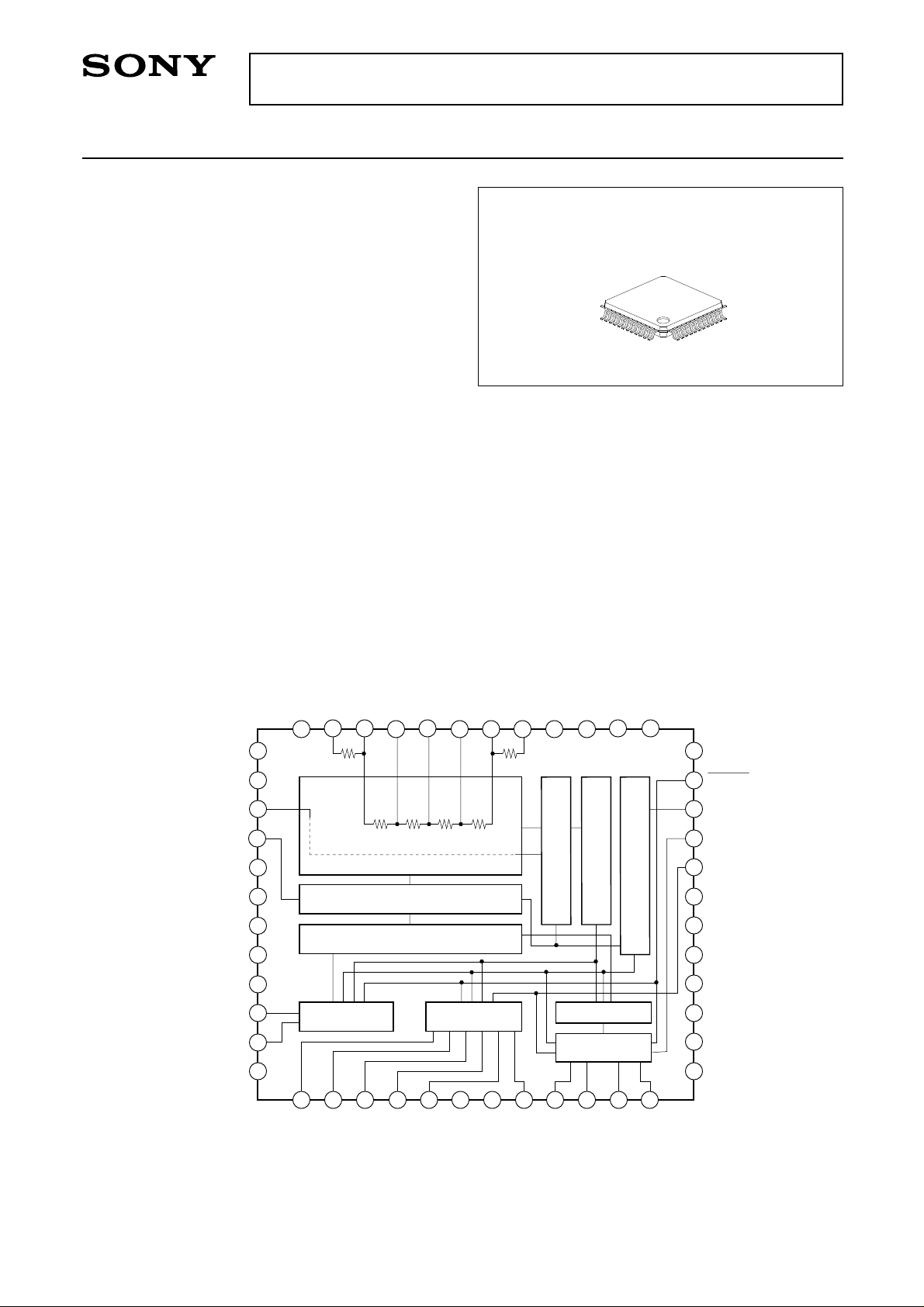
Block Diagram
3
3
CC
CC
DV
N.C.
N.C.
VREFTS
VREFT
VREF1
VREF2
VREF3
VREFB
VREFBS
N.C.
32
33
MATRIX
H-ENCODER
5
4
D3
31
FINE O UTPUT
BUFFER
6
D4
DGND1
30
7
N.C.
28
29
8
D5
27
L-ENCORDER
L-COMPARATOR
CORRECTION
COARSE OUTPUT
BUFFER
9
10
D7
D6
N.C.
N.C.
VINL
VINH
N.C.
AVCC
N.C.
AGND
DVCC2
UNDER
OVER
DGND1
35
36
37
38
39
40
41
42
43
44
45
46
47
48
OVER/UNDER
OUTPUT B UFFER
(LSB) D0
34
H-COMPARATOR
2
3
D1
D2
Sony reserves the right to change products and specifications without prior notice. This information does not convey any license by
any implication or otherwise under any patents or other right. Application circuits shown, if any, are typical examples illustrating the
operation of the devices. Sony cannot assume responsibility for any problems arising out of the use of these circuits.
DV
26
25
PS
24
ENABLE
23
CLK
22
MINV
21
LINV
20
CLK BUFFER
121
11
D8
(MSB) D9
19
18
17
16
15
14
13
N.C.
DV
CC3
DGND2
DGND1
DVCC1
DGND1
N.C.
– 1 –
E94326-PS

Absolute Maximum Ratings (Ta = 25°C)
• Supply voltage DVcc1 0 to +6 V
DVcc2 0 to +6 V
DVcc3 0 to +6 V
AVcc 0 to +6 V
• Analog input voltage VINH AGND to AVcc + 0.3 V
VINL AGND to AVcc + 0.3 V
• Reference voltage VREFT AGND to AVcc + 0.3 V
VREFB AGND to AVcc + 0.3 V
• Digital input voltage CLK DGND1 – 0.5 to DVcc1 V
MINV DGND1 – 0.5 to DVcc1 V
LINV DGND1 – 0.5 to DVcc1 V
PS DGND1 – 0.5 to DVcc1 V
ENABLE DGND1 – 0.5 to DVcc1 V
• Digital output voltage Vo DGND1 – 0.5 to +3.6 V
(Vo: The voltage is applied to the output pin for high impedance output.)
• Storage temperature Tstg –65 to 150 °C
• Allowable power dissipation PD 950 mW
(On a fiber-glass epoxy board: 40mm × 40mm, t = 0.8mm)
CXA1977R
Recommended Operating Conditions
Min. Typ. Max. Unit
• Supply voltage DVcc1 +4.6 +5 +5.25 V
DVcc2 +4.6 +5 +5.25 V
DVcc3 +4.6 +5 +5.25 V
AVcc +4.6 +5 +5.25 V
AGND 0 V
DGND1 0 V
DGND2 0 V
• Analog input voltage VINH +2 +4 V
VINL +2 +4 V
• Reference voltage VREFT +3.9 +4 +4.1 V
VREFB +1.9 +2 +2.1 V
• Digital input voltage VIH +2 V
VIL +0.8 V
• Clock width tPWH 25 ns
tPWL 24 ns
• Operating temperature Topr –20 +85 °C
– 2 –

Pin Description
CXA1977R
Pin No.
1 to 5
8 to 12
46
47
15
45
6, 14,
16, 48
18
25
26
Symbol
I/O
D0 to D9 O
UNDER
OVER
DVCC1
—
DVCC2
DGND1
DVCC3
— GND
—
O
O
Pin voltage
TTL
+5V
(typ.)
+5V
(typ.)
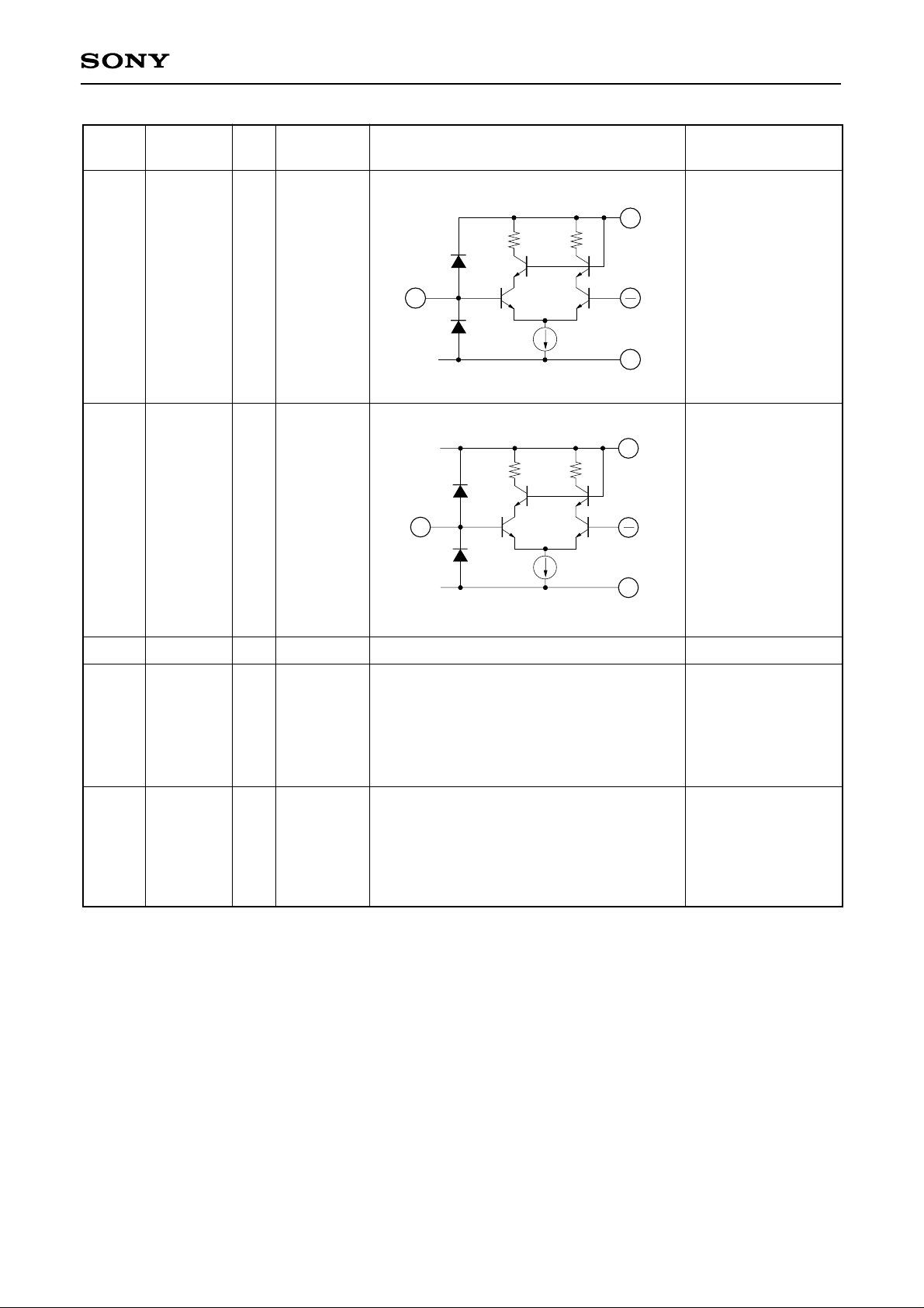
Equivalent circuit
200k
45
1
8
46
47
16
17
DVCC2
D0 to
D5 to
UNDER
OVER
DGND1
DGND2
12
Description
Digital output
D0 (LSB) to
D4
5
D9
D9 (MSB)
Underflow output
Overflow output
Digital power supply
Digital ground
Digital power supply
17
44
20
21
DGND2
AGND
LINV
MINV
23 ENABLE
—
—
Digital negative
power supply
GND
Analog negative
power supply
This input can invert
output form of D0 to
D8. In open
I
condition, this pin
turns to high level
input. (For details,
DV
400k
ENABLE
TTL
I
PS
MINV
LINV
23
24
21
20
100k 100k
refer to the Output
CC1
Formula Chart.)
15
This input can invert
output form of D9
(MSB). In open
condition, this pin
turns to high level
input. (For details,
DGND2
17
DGND1
refer to the Output
16
Formula Chart.)
3-state control.
Turns to enable
I
when low is input.
In open condition,
this pin turns to high
level input.
– 3 –

CXA1977R
Pin No.
24
22
Pin voltage
Symbol
I/O
PS I TTL
CLK I TTL
ENABLE
PS
MINV
LINV
DGND2
CLK
DGND2
Equivalent circuit
23
24
21
20
17
22
17
400k
20k
100k 100k
30k 30k
DVCC1
15
16
DGND1
DVCC1
15
16
DGND1
Description
Power save input.
Power save
condition is entered
when high level is
input. In open
condition, this pin
turns to high level
input.
Clock input
29
30
31
32
33
34
35
VREFTS —
VREFT I
VREF1 —
VREF2 —
VREF3 —
VREFB I
VREFBS —
+4V
+3.5V
+3.0V
+2.5V
+2V
VREFTS
VREFT
VREF1
VREF2
VREF3
VREFB
VREFBS
AGND
29
30
44
31
32
33
34
35
130
130
Reference voltage
sense (Top)
Reference voltage
force (Top)
Reference voltage
force (Bottom)
Reference voltage
sense (Bottom)
– 4 –
CXA1977R
Pin No.
39
40
Pin voltage
Symbol
I/O
VINL I +2V to +4V
VINH I +2V to +4V
VINL
VINH
39
40
Equivalent circuit
11.2k11.2k
26k26k
44
42
42
44
AV
CC
VREF
AGND
CC
AV
VREF
AGND
Description
Analog input
(Lower comparator
input)
Analog input
(Upper comparator
input)
42
7, 13,
19, 27
28, 36,
37, 38,
41, 43
AVCC ——+5V (Typ.)
N.C. —
N.C. —
—
Analog power supply
Open.
Not connected to
internal circuit, but
connection to DGND
(digital ground) is
recommended.
Open.
Not connected to
internal circuit, but
connection to AGND
(analog ground) is
recommended.
– 5 –
 Loading...