

Sony CXA1951AQ Datasheet

GPS Down Converter
Description
The CXA1951AQ is an IC developed as a GPS
down converter, featuring low current consumption
and small package. This IC is suitable for the
mobile GPS (Global Positioning System).
Features
• Includes all functions required for the GPS converter
• Total gain: 100 dB or more
• Operating supply voltage range: 2.7 to 5.5 V
• Low current consumption:
ICC = 30 mA (Typ. at VCC = 3 V)
• Excellent temperature characteristics
Applications
GPS (Global Positioning System)
CXA1951AQ
40 pin QFP (Plastic)
Absolute Maximum Ratings (Ta = 25 °C)
• Supply voltage VCC 7.0 V
• Operating temperature Topr –40 to +85 °C
• Storage temperature Tstg –65 to +150 °C
• Allowable power dissipation
PD 200 mW
Structure
Bipolar silicon monolithic IC
Operating Conditions
Supply voltage VCC 2.7 to 5.5 V
Sony reserves the right to change products and specifications without prior notice. This information does not convey any license by
any implication or otherwise under any patents or other right. Application circuits shown, if any, are typical examples illustrating the
operation of the devices. Sony cannot assume responsibility for any problems arising out of the use of these circuits.
—1—
E96743-TE

Block Diagram and Pin Configuration
LIM DEC2
LIM DEC1
LIM IN
CC
LIM V
CC
IF V
IF OUT
IF DEC2
IF DEC1
IF IN2
CXA1951AQ
IF IN1
21222324252627282930
LIM OUT
LIM GND
N.C
REF INV
REF IN
PLL GND
FC
TEST OUT
LOCK DET
PLL V
CC
31
32
33
34
35
36
37
38
39
1/4 or 1/6
PLL
1/338 or 1/570
OSC
20
19
18
17
16
15
14
13
12
40 11
1 2 3 4 5 6 7 8 9
CP OUT
N.C
OSC GND
OSC GND
OSCB1
OSCE1
OSCE2
NSW
10
OSCB2
OSC GND
IF GND
RF OUT2
RF OUT1
RF VCC
RF IN2
RF IN1
RF GND
RF GND
OSC DEC
OSC V
CC
—2—
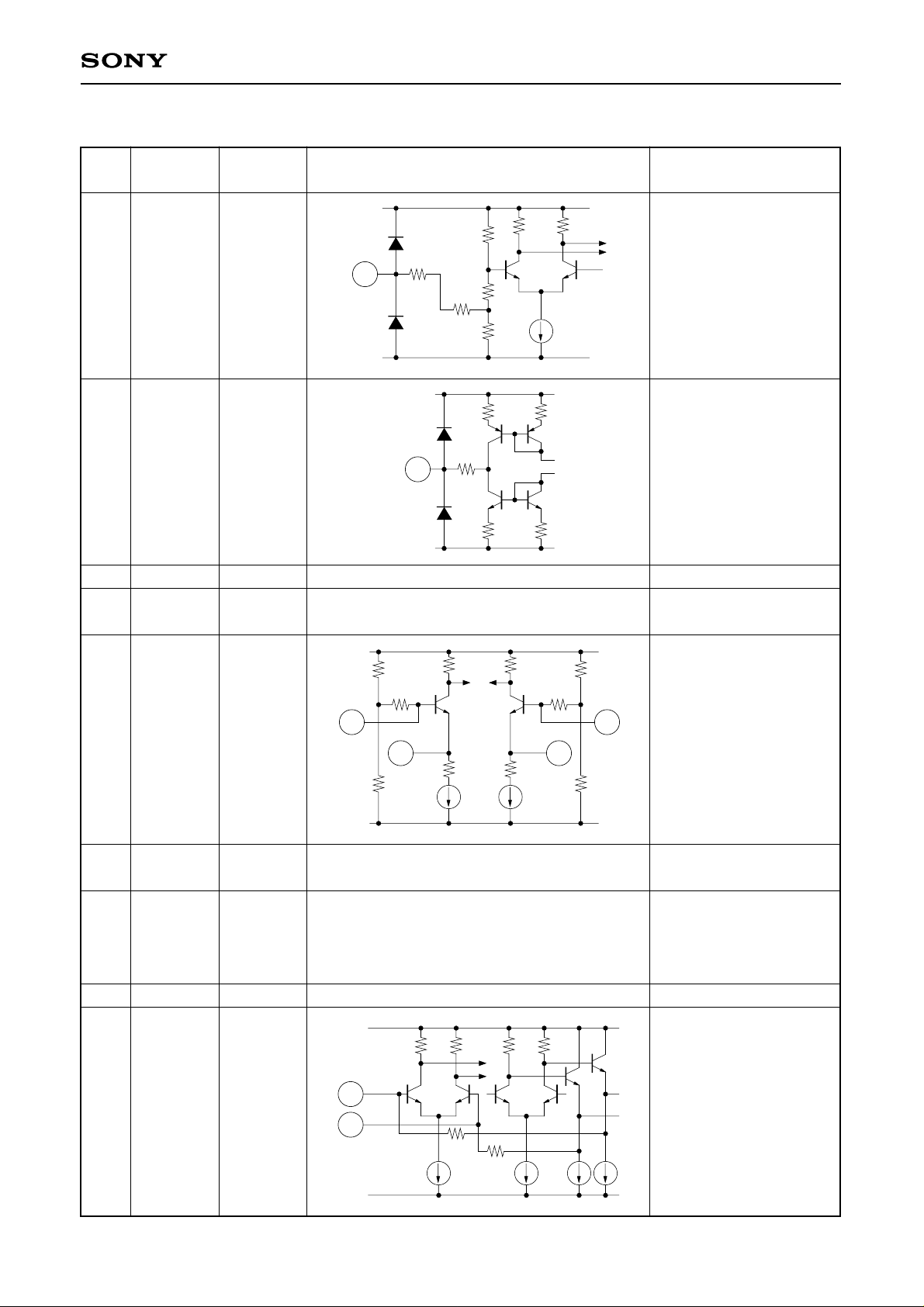
Pin Description
CXA1951AQ
Pin
No.
1
2
3, 33
4, 5,
10
Symbol Pinvoltage Equivalent circuit Description
VCC
40k
200
VCC
2
GND
20k
200
40k
81k
Internal PLL frequency
division value switching
Charge pump output
Not connected
Ground for the internal
oscillator
NSW
CPOUT
NC
OSC GND
—
1
GND
—
—
0 V
6
9
7
8
11
12
13, 14
15, 16
OSCB1
OSCB2
OSCE1
OSCE2
OSC VCC
OSC DEC
RF GND
RF IN1
RF IN2
2.5 V
1.7 V
1.7 V
2.5 V
3 V
1.7 V
0 V
1.6 V
1.6 V
CC
V
6
GND
VCC
15
16
1.6k 1.6k
1k 1k
7 8
12k 12k
12k
12k
Connects the internal
9
oscillator resonator.
Connects to main
counter input via the
internal buffer.
Internal oscillator power
supply
Connects decoupling
capacitor for the internal
oscillator bias power
supply
RF amplifier ground
RF amplifier input.
When using as a single
input, ground Pin 16 via
the capacitor.
GND
—3—

CXA1951AQ
Pin
No.
17
18, 19
20
21, 22
23, 24
Symbol Pinvoltage Equivalent circuit Description
RF VCC
RF OUT1
RF OUT2
IF GND
IF IN1
IF IN2
IF DEC1
IF DEC2
3 V
—
—
0 V
1.9 V
1.9 V
1.9 V
1.9 V
GND
VCC
21
22
GND
2k
990
990
200
23 24
200
VCC
19
18
99k
99k
RF amplifier power
supply
RF amplifier mixer
output
IF amplifier ground
IF amplifier input
IF amplifier decoupling
25
26
27
28
29, 30
IF OUT
IF VCC
LIM VCC
LIM IN
LIM DEC1
LIM DEC2
2.7 V
3 V
3 V
2.1 V
2.1 V
2.1 V
V
CC
GND
28
30
GND
VCC
1k
200 96k
990
200
1k
96k
25
IF amplifier mixer
output
IF amplifier power
supply
Limiter buffer power
supply
Limiter input
29
Limiter decoupling
—4—

CXA1951AQ
Pin
No.
31
32
34
35
36
Symbol Pinvoltage Equivalent circuit Description
VCC
LIM OUT
LIM GND
31
GND
0 V
Limiter buffer output
Limiter buffer ground
Reference frequency
CC
V
signal output.
The reference frequency
REF INV
High: 2.2 V
Low: 2.0 V
35
200
39.6k
39.6k
200
34
signal can also be made
by connecting this pin
and Pin 35 with a crystal
oscillator to configure an
oscillator.
Reference frequency
input and reference
REF IN
2.1 V
GND
counter input
PLL GND
0 V
PLL ground
37
38
FC
TEST OUT
—
High: 2.2 V
Low: 2.0 V
GND
VCC
GND
V
37
CC
200
100k
100k
81k
200
38
Switching for the charge
pump output status and
for the signal output to
Pin 38
Output of the frequency
division signal by the
counter
—5—
 Loading...