

Sony CXA1946BR, CXA1946BQ Datasheet

CXA1946BQ/BR
For the availability of this product, please contact the sales office.
Electronic Volume
Description
The CXA1946BQ/BR is a serial control electronic
volume IC designed for use in audio systems.
Features
• Loudness
• Volume control (0dB to –87dB in 1dB step, –∞dB)
• Balance
• Tone control (15 steps, 2 bands, –16dB to +16dB)
• Fader
(2dB-step to –20dB, –25dB, –35dB, –45dB, –60dB, –∞dB)
• Input selector (4 channels)
• Gain can be set for each input channel (common for channels 3 and 4)
• Serial data control (DATA, CLK, CE)
• Single 8V power supply
• Zero-cross detection circuit (with timer)
• Power-off mute
• Volume control and tone control input/output pins are separate.
• Portable phone noise countermeasure
48 pin QFP (Plastic)
48 pin LQFP (Plastic)
Absolute Maximum Ratings
• Supply voltage VCC 13 V
• Operating temperature Topr –40 to +85 °C
• Storage temperature Tstg –65 to +150 °C
• Allowable power dissipation PD 350 mW (Ta = 85°C)
Operating Conditions
Supply voltage VCC 6 to 12 V
Sony reserves the right to change products and specifications without prior notice. This information does not convey any license by
any implication or otherwise under any patents or other right. Application circuits shown, if any, are typical examples illustrating the
operation of the devices. Sony cannot assume responsibility for any problems arising out of the use of these circuits.
– 1 –
E96X03A7Y

Block Diagram and Pin Configuration
CXA1946BQ/BR
GAIN12
GAIN11
IN14
IN13
IN12
IN11
IN21
IN22
44
37
38
39
40
41
42
43
GAIN134
36
INPUT SW
LDLC1
35
ZCDET
LOUD
LDHC1
34
INAO1
33
8dB STEP
VOLUME
VRIN1
32
LATCH
SHIFT REGISTER
VOUT1
31
1dB STEP
VOLUME
VCTBUFF
VCTBUFF
VCTBUFF
30
TIN1
TCHC1
29
LATCH CONTROL
28
TONE
TCLC11
TCLC12
27
26
TCO1
FADER
100k
100k
FDIN1
25
24
23
22
21
20
19
18
17
FNTO1
REO1
CE
CLK
DGND
GND
CC
V
VCT
IN23
IN24
GAIN21
GAIN22
45
46
47
48
INPUT SW
GAIN234
2
LDLC2
LOUD
3
LDHC2
VOLUME
8dB STEP
4
INAO2
5
VRIN2
VCTBUFF
VCTBUFF
VCTBUFF
VOLUME
1dB STEP
6
VOUT2
7
TIN2
8
TCHC2
TONE
9
TCLC21
10
TCLC22
11
FADER
TCO2
121
FDIN2
16
15
14
13
DATA
TIMER
REO2
FNTO2
– 2 –
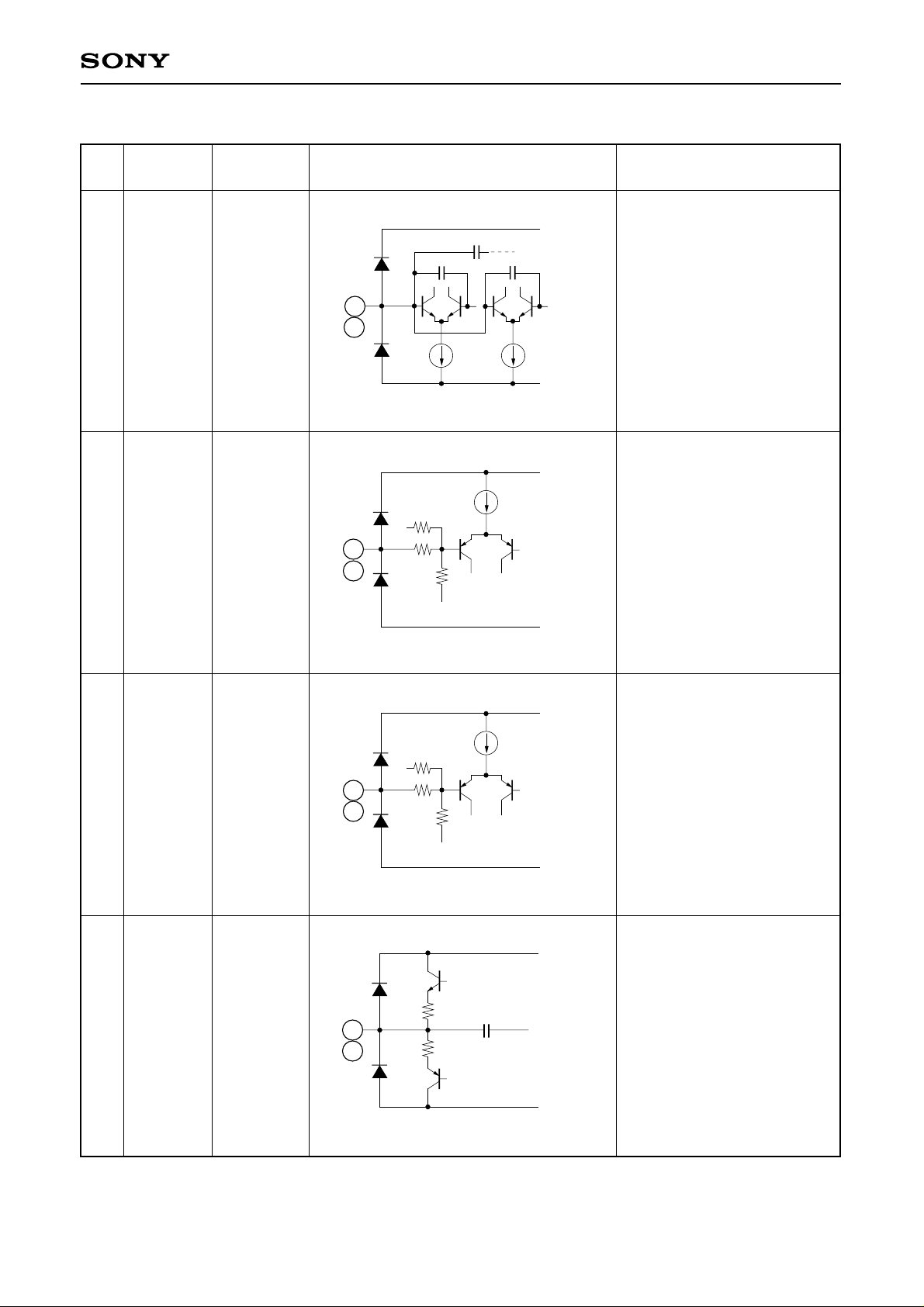
Pin Description
CXA1946BQ/BR
Pin
No.
1
36
2
35
Symbol
GAIN234
GAIN134
LDLC2
LDLC1
I/O resistance
Pin voltage
~
∞
–
VCT
6.18kΩ
VCT
36
35
Equivalent circuit
V
CC
1
GND
CC
V
2
Sets gain for IN3 and IN4.
Sets loudness low cut-off
frequency.
Description
3
34
4
33
LDHC2
LDHC1
INAO2
INAO1
8.92kΩ
VCT
—
VCT
33
3
34
GND
V
CC
Sets loudness high cut-off
frequency.
GND
V
CC
4
Input selector output
– 3 –
GND
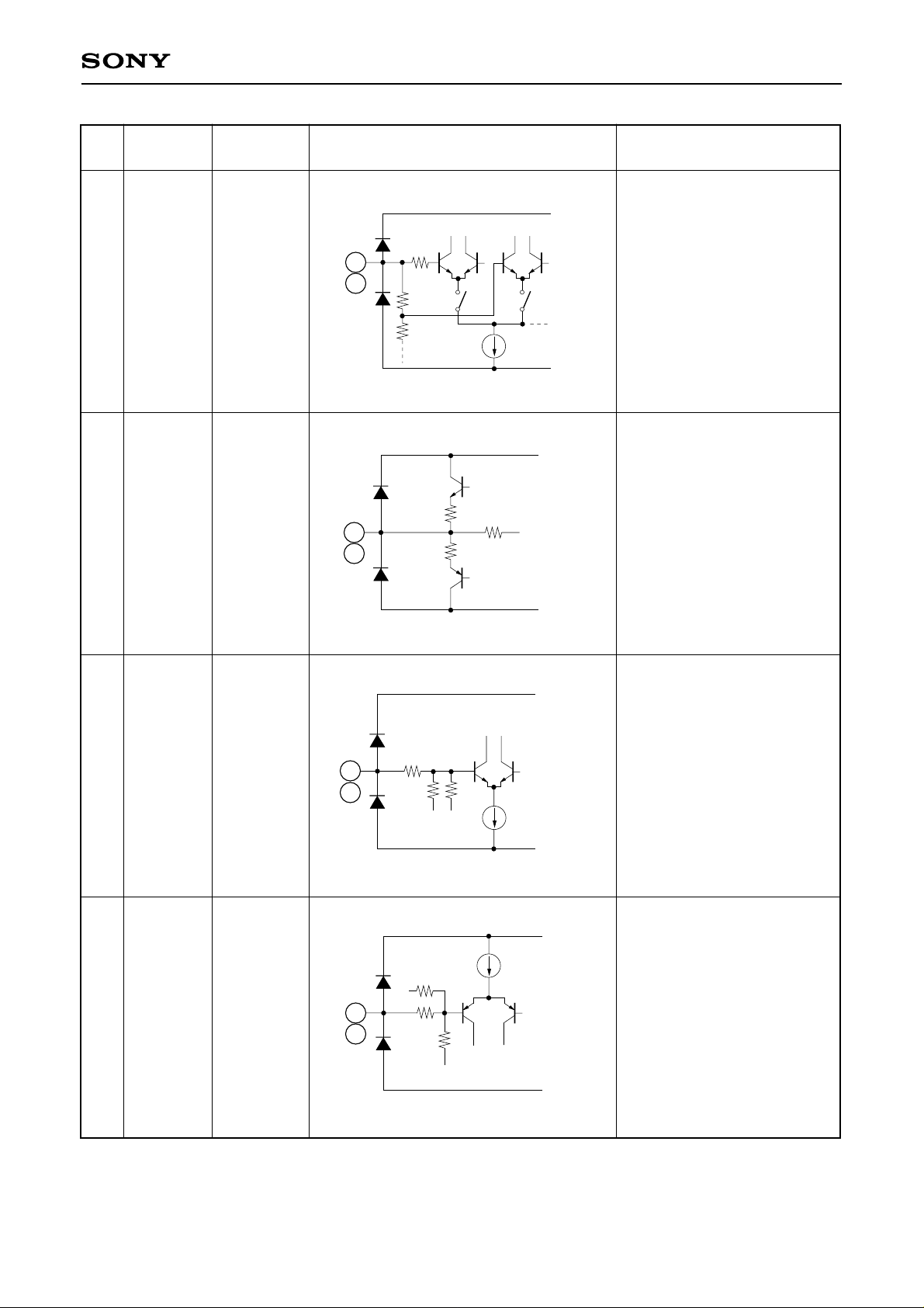
CXA1946BQ/BR
Pin
No.
5
32
6
31
Symbol
VRIN2
VRIN1
VOUT2
VOUT1
I/O resistance
Pin voltage
9.5kΩ
VCT
—
VCT
32
31
Equivalent circuit
CC
V
5
Description
Volume input
GND
VCC
6
Volume output
7
30
8
29
TIN2
TIN1
TCHC2
TCHC1
19kΩ
VCT
5kΩ
VCT
30
7
29
GND
V
CC
Tone input
GND
V
CC
8
Sets tone high frequency.
– 4 –
GND
CXA1946BQ/BR
Pin
No.
9
28
10
27
Symbol
TCLC21
TCLC11
TCLC22
TCLC12
I/O resistance
Pin voltage
8kΩ
VCT
8kΩ
VCT
28
Equivalent circuit
V
CC
9
GND
CC
V
10
27
Sets tone low frequency.
Sets tone low frequency.
Description
11
26
12
25
TCO2
TCO1
FDIN2
FDIN1
—
VCT
24kΩ
VCT
12
11
26
25
GND
VCC
GND
V
CC
Tone control output
Fader input
– 5 –
GND
CXA1946BQ/BR
Pin
No.
13
24
14
23
Symbol
FNTO2
FNTO1
REO2
REO1
I/O resistance
Pin voltage
—
VCT
—
VCT
14
13
23
24
Equivalent circuit
V
CC
GND
VCC
Description
Front output
Rear output
15
16
TIMER
DATA
GND
VCC
—
—
~
∞
–
—
15
16
Sets timer.
GND
VCC
Serial data input
– 6 –
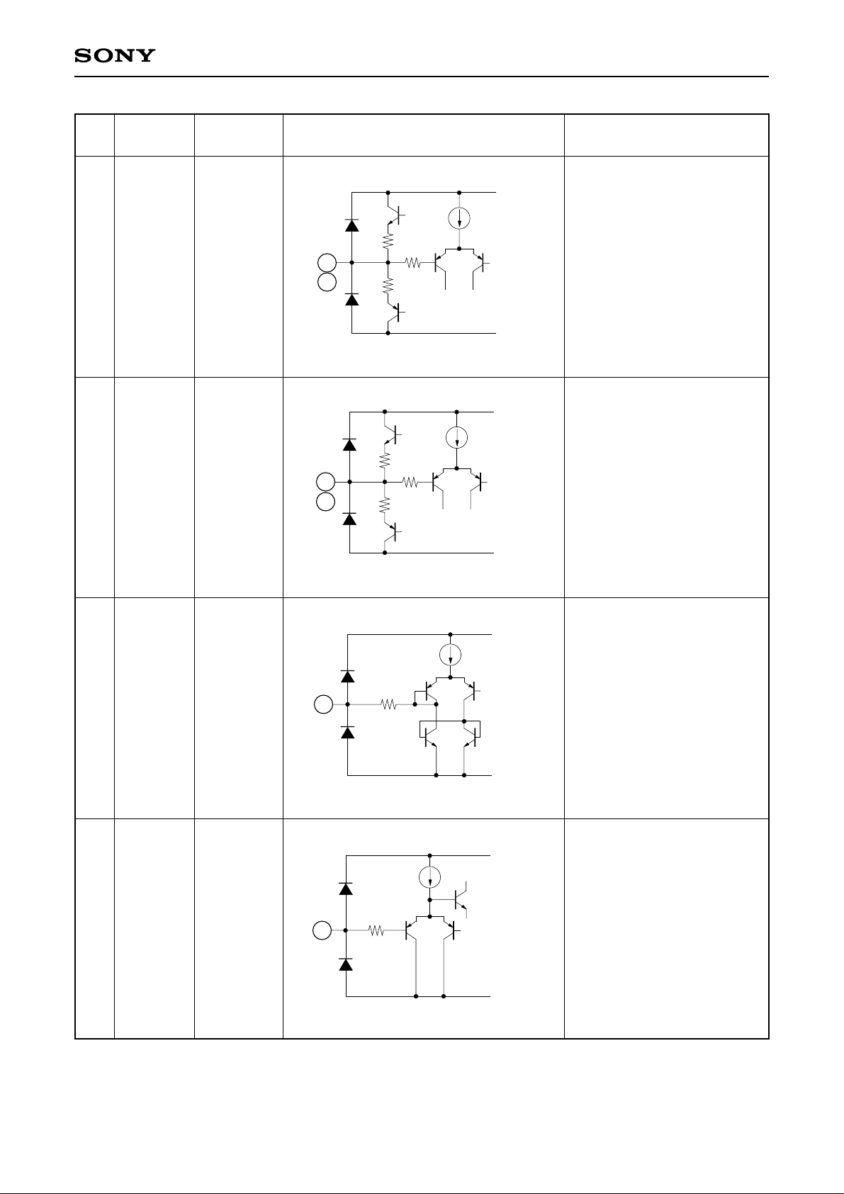
GND

CXA1946BQ/BR
Pin
No.
17
18
19
20
21
Symbol
VCT
VCC
GND
DGND
CLK
I/O resistance
Pin voltage
—
VCT
VCC
GND
—
~
∞
–
—
21
Equivalent circuit
V
CC
GND
VCC
Description
Center electric potential
+ power supply
GND
Digital GND
Serial clock input
22
37
48
CE
GAIN12
GAIN22
~
∞
–
—
~
∞
–
VCT
37
48
22
Latch enable input
GND
VCC
Sets gain for IN2.
GND
– 7 –
 Loading...