

Sony CXA1911Q Datasheet

CXA1911Q
For the availability of this product, please contact the sales office.
Dolby B/C Type Noise Reduction System with Playback Equalizer
Description
The CXA1911Q is an IC designed for use in car
stereo cassette decks. Functions include Dolby B/C
type noise reduction, playback equalizer amplifier
and music sensor into a single chip.
Features
• Few external parts
• Forward/Reverse head switching
• Small package (40-pin QFP)
• Dolby B/C type noise reduction and playback
equalizer into a single chip
• Same pin configuration as Dolby B type noise
reduction system (CXA1910Q)
• Music sense level can be set by external
resistors/capacitors (2 modes).
• High-band cut filter frequency can be adjusted by
the external capacitance.
Absolute Maximum Ratings (Ta=25°C)
• Supply voltage VCC 12 V
• Operating temperature Topr –40 to +85 °C
• Storage temperature Tstg –65 to +150 °C
• Allowable power dissipation
Recommended Operating Conditions
• Supply voltage VCC 7.8 to 11 V
40 pin QFP (Plastic)
PD 430 mW
Applications
• Car stereo cassette decks
• Cassette decks (playback only)
Structure
Bipolar silicon monolithic IC
∗ These ICs are available only to the licensees of Dolby Laboratories Licensing Corporation from whom licensing and applications
information may be obtained.
∗ "Dolby" and the double D symbols are trade marks of Dolby Laboratories Licensing Corporation.
∗ Sony reserves the right to change products and specifications without prior notice. This information does not convey any license
by any implication or otherwise under any patents or other right. Application circuits shown, if any, are typical examples
illustrating the operation of the devices. Sony cannot assume responsibility for any problems arising out of the use of these
circuits.
—1—
E93Y13-TE
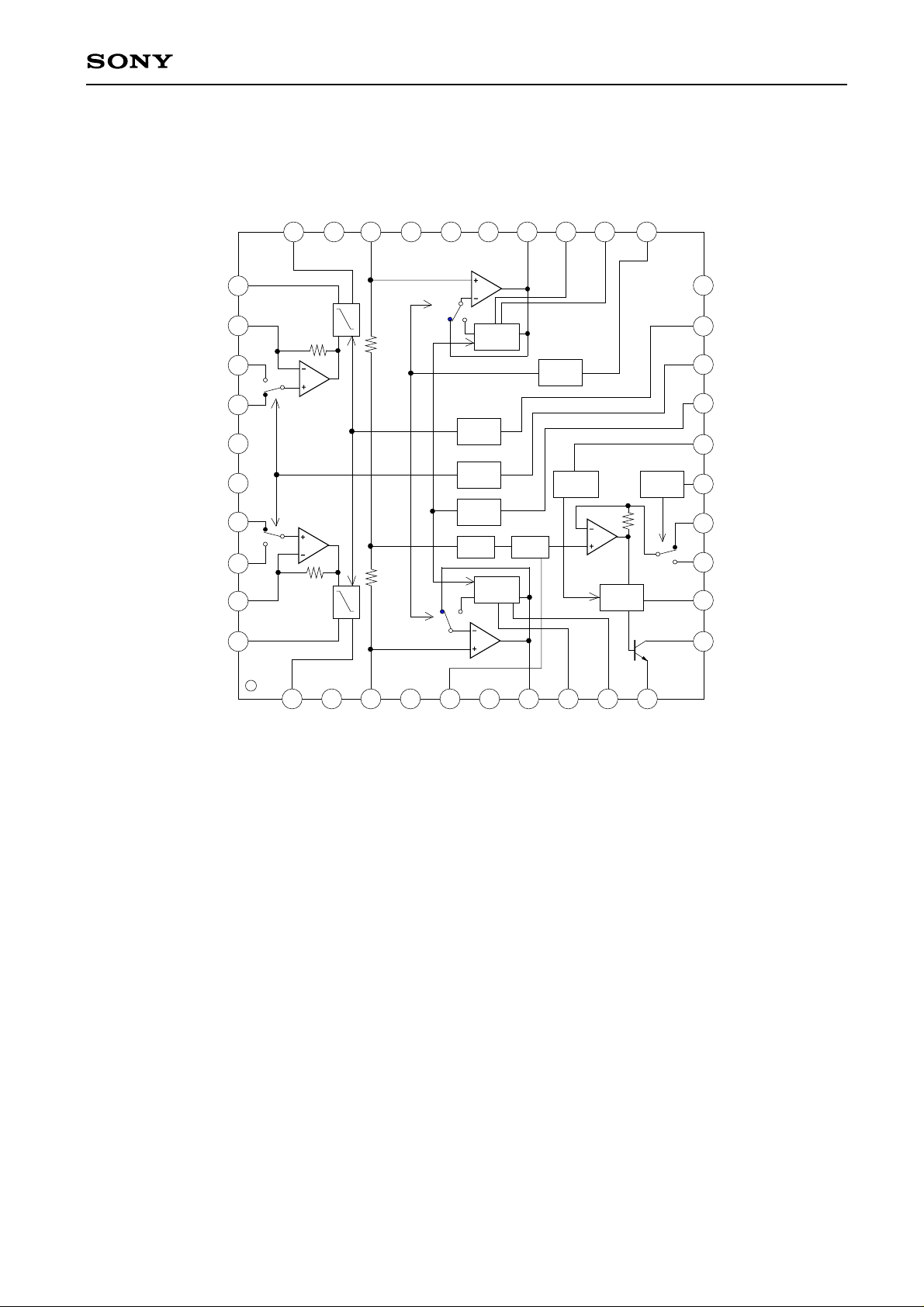
Block Diagram
PBFIN1
PBGND
PBFIN2
PBTC1
PBFB1
PBRIN1
E IREF
PBRIN2
PBFB2
PBTC2
CXA1911Q
NRSW
TCH1
TCL1
LINEOUT1
VCT
NC
NC
TAPEIN1
GND
PBOUT1
31
32
33
34
35
36
37
38
39
40
300k
F/R
F/R
300k
TAPE
DR
NR
10dB
NR
IN
LPF
NR
AMS
22 212324252627282930
DET
MODE
G1/G2
NC
20
TAPESW
19
DRSW
18
NRMODE
17
MSSW
16
MSMODE
15
G1 (FF)
14
G2 (NOR)
13
MSTC
12
MSOUT
11
1 2 3 4 5 6 7 8 9 10
Vcc
PBOUT2
NC
D IREF
TAPEIN2
MS LPF
TCL2
TCH2
LINEOUT2
MSGND
—2—
CXA1911Q
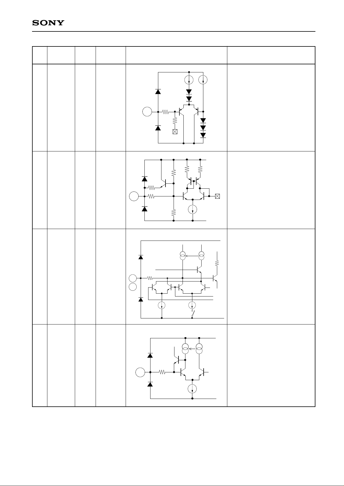
Pin Description (Ta=25°C, VCC=8.0V, no signal)
Pin
Symbol
No. value
DC
Z (in) Equivalent circuit Description
1 PBOUT 2.1V —
30
32 PBFB 2.1V 300kΩ
39
33 PBIN 0V —
34
37
38
2VCC 8.0V —
3 TAPEIN 4.0V 40kΩ
28
Refer to Page 7.
3
28
147
VGS
PBEQ output
PBEQ feedback
PBEQ input
Power supply
TAPE input
40k
12µA
4NC — —
20
26
27
5 MSLPF 4.0 100kΩ
No connection
Adjustment of MS LPF
VCC
100k
5
147
64p
GND
frequency
—3—
CXA1911Q
Pin
Symbol
No. value
DC
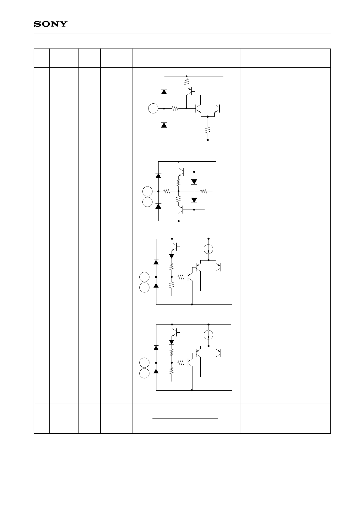
6 D IREF 1.25V —
7 LINEOUT 4.0V —
24
Z (in) Equivalent circuit Description
Connection of reference
current setting resistor for
Dolby block
6
147
50k
Line output
VCC
147
7
24
200
200
GND
8 TCL 0.3V —
23
9 TCH 0.3V —
22
10 MSGND 0.0V —
29 GND
35 PBGND
23
22
Time Constant pin for the LLS
8
13.5k
147
480k
Time Constant pin for the HLS
36k
9
147
330k
Ground
—4—
CXA1911Q
Pin
Symbol
No. value
DC
Z (in) Equivalent circuit Description
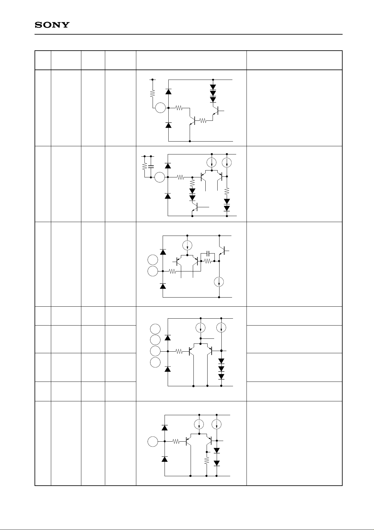
11 MSOUT 0.2 V —
for signal
detection;
5.0 V for
no signal
detection
12 MSTC Approx. —
1.4 V for
signal
detection;
5.0 V for
no signal
detection
13 G2(NOR) 4.0V —
14 G1(FF)
VDD=5V
VDD=5V
11
12
147
147
1k
10µ
20k
VCC
GND
VCC
50µ
GND
MS output
Connection of MS detection time
Vcc
constant
MS feedback
15 MSMODE — —
18 DRSW
19 TAPESW
21 NRSW
16 MSSW — —
13
14
16
15
18
19
21
147
147
147
100k
50µ
50µ
100µ
GND
50µ
50µ
VCC
MSMODE MS gain selector
G1 when high, G2 when low
DRSW Head selector
Reverse when high, Forwards
when low
TAPESW Equalizer selector
120µs when high, 70µs when
low
NRSW NR ON/OFF selector
MS on/off selector
MS on when high, MS off when
low
—5—
GND
CXA1911Q
Pin
Symbol
No. value
DC
Z (in) Equivalent circuit Description
17 NRMODE — —
25 VCT 4.0V —
25
17
147
45k
147
Q3
50k
2.5V
30k
30k
50µ
Noise reduction selector
C when high, B when low
50µ
VCC/2 output
to VGS
31 PBTC — —
40
36 E IREF 1.25V —
PBEQ capacitance
CC
V
147
31
40
42µ
30µ
GND
Connection of reference current
V
CC
36
147
1.25V
10µ
GND
setting resistor for PBEQ block
—6—
 Loading...