

Sony CXA1897Q Datasheet

—1—
E93930D78
Sony reserves the right to change products and specifications without prior notice. This information does not convey any license by
any implication or otherwise under any patents or other right. Application circuits shown, if any, are typical examples illustrating the
operation of the devices. Sony cannot assume responsibility for any problems arising out of the use of these circuits.
Dolby B Type Noise Reduction System with Recording/Playback Equalizer
CXA1897Q
Absolute Maximum Ratings (Ta=25°C)
• Supply voltage VCC 12 V
• Operating temperature Topr –20 to +75 °C
• Storage temperature Tstg –65 to +150 °C
• Allowable power dissipation
PD 735 mW
Operating Conditions
• Supply voltage VCC 6.5 to 10.0 V
Description
The CXA1897Q is an analog signal processing IC
for tape recorders. It achieves whole processing
operations for the recording and playback systems
which include the Dolby B noise reduction function
on a single chip. This IC supports 2 channels at
each function.
Features
• Dolby B noise reduction supports 1.7 times normal
speed.
• Recording/playback equalizer amplifier supports
1.7 times normal speed.
• Built-in comparator for AMS (automatic music
sensor)
• Built-in AGC (automatic gain control) with amplifier
for MPX filter.
• Playback equalizer outputs independently for
DECK-A and DECK-B.
• Externally adjustable recording equalizer Gp and
fp.
• Built-in Recording mute function.
• Double cassette dubbing system can be easily
configured just with this IC.
Applications
All analog signal processing in cassette deck parts
of tape recorders and compact music centers
(Sankyo Seiki mfg. Co., Ltd. YK47R-KF202 or
equivalent which has the same head type.)
Structure
Bipolar silicon monolithic IC
48 pin QFP (Plastic)
∗ These ICs are available only to the licensees of Dolby Laboratories Licensing Corporation from whom licensing and applications
information may be obtained.
∗ "Dolby" and the double D symbols are trade marks of Dolby Laboratories Licensing Corporation.

—2—
CXA1897Q
Block Diagram
AMS
OUT
GND
D PB IN1
DOLBY NR
ON/OFF/HI
D L OUT1
Vcc
Vcc
AGC IN
GND
+
+
AMS GAIN
GND
MPX
D REC IN1
GND
D IREF
GND
RFC
AGC
+
OUT
TC
DECK A
PB FB11
PB HEAD
GND
PB INA1
PB INB1
PB INB2
PB INA2
GND
++
PB FB12
GND
++
PB OUTA2
PB FB22
PB OUTB2
GND
PB OUTB1
GND
PB OUTA1
PB FB21
373839404142434445464748
GND
GND
GND
1
2
3
10dB
AMP
IREF
AGC
IREF
AMS
4
+
10k
5
40k
6
7
8
+ +
9
10
11
12
NR
REC
EQ
PBEQ
CTL
GND
GND
MUTE
REC
EQ
RECEQ
CTL
GND
10dB
AMP
40k
NR
Vcc
GND
10k
GND
36
35
IREF
34
VG
33
+
32
31
AGC
OUT
30
D REC IN2
29
+ +
28
27
26
25
TC
GND
++
AGC TC
GNDGND GND
AGC IN
MPX
+
+
GND
REC
MUTE
GND
D PB IN2
DOLBY NR
REC/PB
D L OUT2
GND
GND
13
+
D R OUT1
GND
GND
+
DECK
REC IN
PB
REC
(120/70us)
DECK
A EQ
A/B
(N/Cr/Me)
DECK B EQ
REC OUT1
DECK B
R/P HEAD
++
REC OUT2
FP CAL
SPEED
GNDGND
PB
REC
+
GP CAL
GNDGND
REC IN
2423222120191817161514
+
D R OUT2
GND
—3—
CXA1897Q
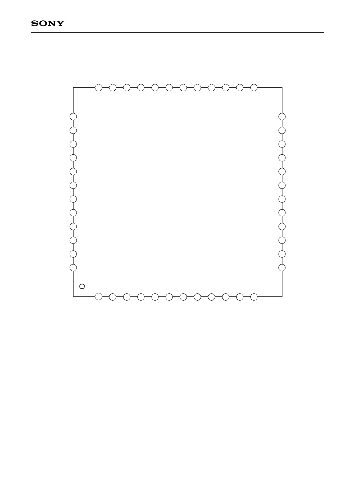
Pin Configuration
37
PB OUTB2
38
PB OUTA2
39
PB FB22
40
PB FB12
41
PB INB2
42
PB INA2
43
PB INA1
44
PB INB1
45
PB FB11
46
PB FB 21
47
PB OUTA1
GND
3536
IREF
34
VG
33
AGC TC
32
AGC IN2
31
30
AGC OUT2
CXA1897Q
29
D RECIN2
REC MUTE
28
D PBIN2
27
MODE
26
25
D L OUT2
D TC2
D R OUT2
REC IN2
GP CAL
FP CAL
SPEED
REC OUT2
REC OUT1
B EQ
A EQ
DECK AB
REC IN1
24
23
22
21
20
19
18
17
16
15
14
48
PB OUTB1
1
Vcc
RFC
AMS OUT
32
4
AMS GAIN
AGC IN1
5
AGC OUT1
6
D RECIN1
D IREF
87
D PBIN1
9
NRSW
10
D L OUT1
11 12
D R OUT1
D TC1
13
—4—
CXA1897Q
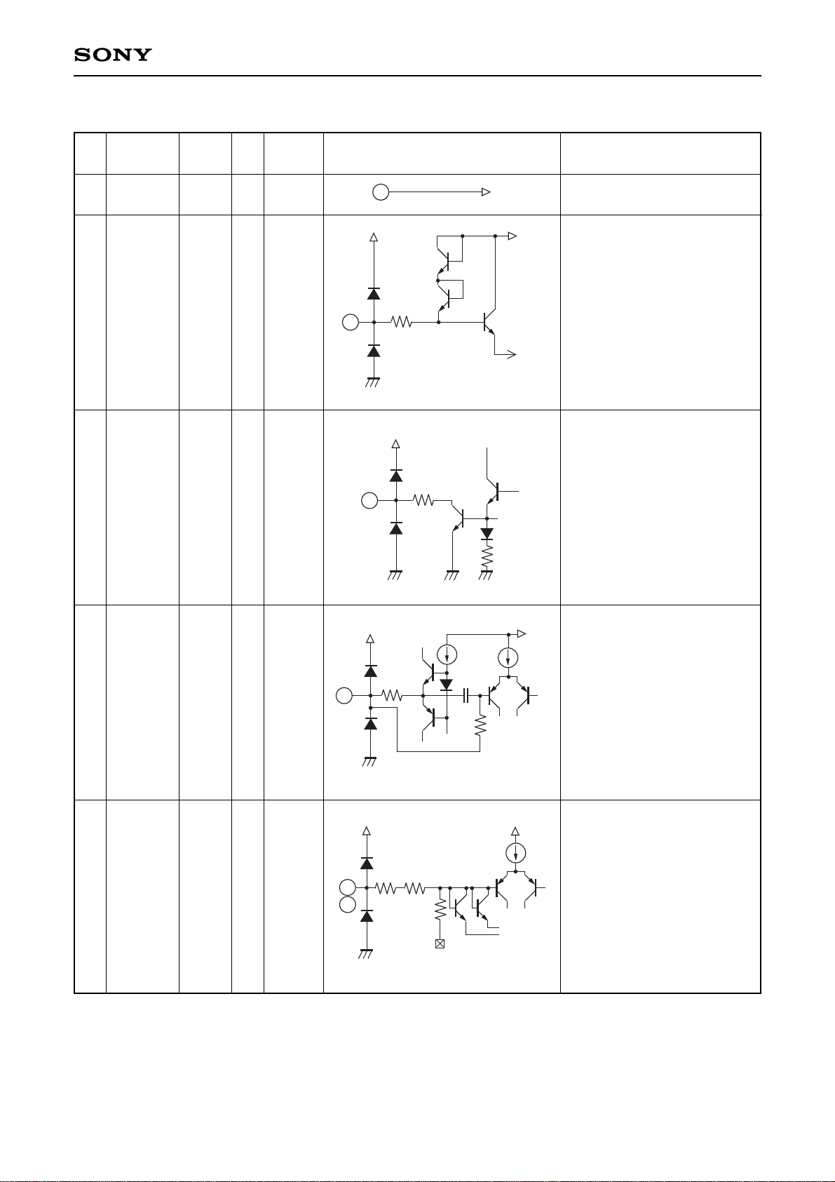
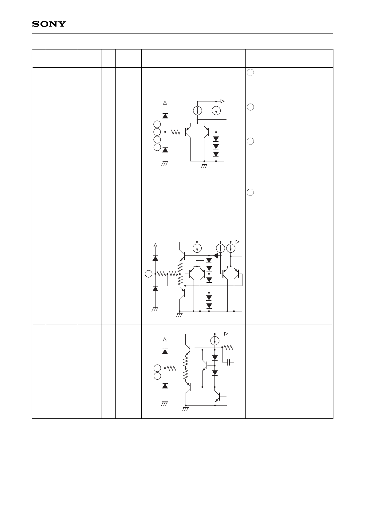
Pin Description (Ta=25°C, Vcc=8 V, no signals)
Pin
Symbol
DC
I/O
I/O
Equivalent circuit Description
No. voltage
resistance
1 Vcc 8.0V — —
2 RFC 8.0V — —
3 AMS OUT 8.0V O —
4 AMS GAIN 2.8V — —
5 AGC IN1 4.0V I 50kΩ
32 AGC IN2
Power supply pin.
Connects the resistor and
capacitor for providing a ripple
eliminated stable voltage in
the power supply.
AMS output pin.
Connects the resistor and
capacitor which determine the
attack and recovery time
constants of the output to Vcc.
No signal supplied → High
level
Signal supplied → Low level
Connects the resistor which
determines the AMS signal
detection level.
AGC signal input pin.
The input resistance varies
from 50kΩ to 10kΩ.
AGC is applied when a signal
of –30dB or more level is input
to AGC.
(Pin 33 external 47µF //
300kΩ)
1
Vcc
Vcc
×3
×3
2
147
GND
Vcc
×250
to RFS
Vcc
3
147
×2
GND
Vcc
Vcc
4
32
5
GND
Vcc
GND
147
147
×2
10k
40k
VGS
×4
5p
10k
Vcc
—5—
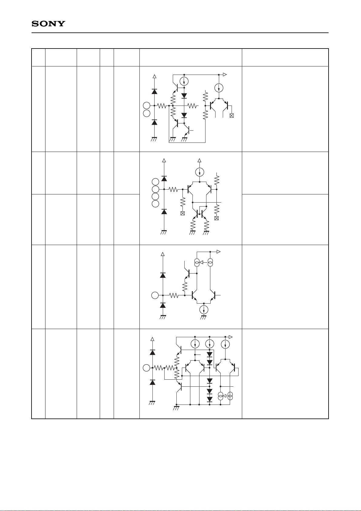
CXA1897Q
Pin
Symbol
DC
I/O
I/O
Equivalent circuit Description
No. voltage
resistance
6
AGC OUT1
4.0V O 147Ω
31
AGC OUT2
7 D RECIN1 4.0V I 40kΩ
30 D RECIN2
9 D PBIN1 4.0V I 40kΩ
28 D PBIN2
8 D IREF 1.2V — —
10 NRSW 2.5V I 53kΩ
(For
OPEN)
AGC output pin.
Dolby NR recording
(encoding) input pin.
Dolby NR playback (decoding)
input pin.
Connects the 18kΩ resistor for
providing the reference
current of the Dolby NR
section internal filter.
Dolby NR ON/OFF switch.
Low : ON
Medium :OFF
High : 1.7 times normal
speed
Vcc
GND
147
4k
×2
×4
Vcc
8
Vcc
GND
147
50k
5k
5k
10
GND
Vcc
6
31
Vcc
GND
7
9
28
30
147
Vcc
GND
×2
×4
147
40k
500
500
VGS
15k
21k
10k
5k
Vcc
15k
Vcc
VGS
VGS
—6—
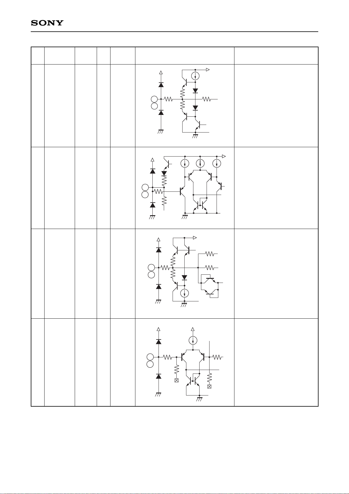
CXA1897Q
Pin
Symbol
DC
I/O
I/O
Equivalent circuit Description
No. voltage
resistance
11 D L OUT1 4.0V O 147Ω
26 D L OUT2
12 D TC1 0.3V — —
25 D TC2
13 D R OUT1 4.0V O 147Ω
24 D R OUT2
14 REC IN1 4.0V I 50kΩ
23 REC IN2
Dolby NR line (decoding)
output pin.
Connects the capacitors
(0.1µF) which determine the
time constants of the input
signal level detector.
Dolby NR recording
(encoding) output pin.
Recording equalizer input pin.
11
26
Vcc
147
×2
200
200
×10
Vcc
6k
12
25
GND
Vcc
×2
20k
147
700k
GND
Vcc
GND
GND
14
23
13
24
Vcc
GND
Vcc
GND
147
×10
147
×2
50k
300
300
VGS
Vcc
10k
13k
GND
Vcc
23k
1.8k
VGS
GND
—7—
CXA1897Q
Pin
Symbol
DC
I/O
I/O
Equivalent circuit Description
No. voltage
resistance
15 DECK AB — I —
16 A EQ
20 SPEED
27 MODE
17 B EQ 2.5V I 53kΩ
(For
OPEN)
18 REC OUT1 4.0V O 147Ω
19 REC OUT2
15
Playback input deck A/B
selector switch
Low : PB INA
High : PB INB
16
Deck A equalizer selector
switch.
Low : 120µs EQ
High : 70µs EQ
20
Recording/playback
equalizer speed selector
switch.
Low : Normal speed
High : High speed
(1.7 times normal speed)
27
Dolby NR mode selector
switch.
Low : Recording
(encoding)
High : Playback (decoding)
Deck B equalizer selector
switch.
Low : Normal tape, 120µs
EQ
Medium :CrO2 tape, 70µs EQ
High : Metal tape, 70µs
EQ
Recording equalizer output.
Vcc
GND
147
50k
5k
5k
GND
Vcc
17
19
Vcc
GND
147
500
GND
Vcc
500
×3
×10
×2
40k
5p
18
Vcc
Vcc
15
16
20
27
147
GND
GND
 Loading...