

Sony CXA1884N Datasheet
Low-voltage FM IF Amplifier
Description
The CXA1884N is designed for FM communication
devices. They incorporate a paging system, mixer, IF
limiter, FM detector, operational amplifier, comparator,
and others.
Features
• Low operating voltage 1.0 to 4.0V
• Low power consumption 2mA at 1.5V
• Built-in power source voltage monitor
Applications
IF Amplifier for Paging System Receiver
Structure
Bipolar silicon monolithic IC
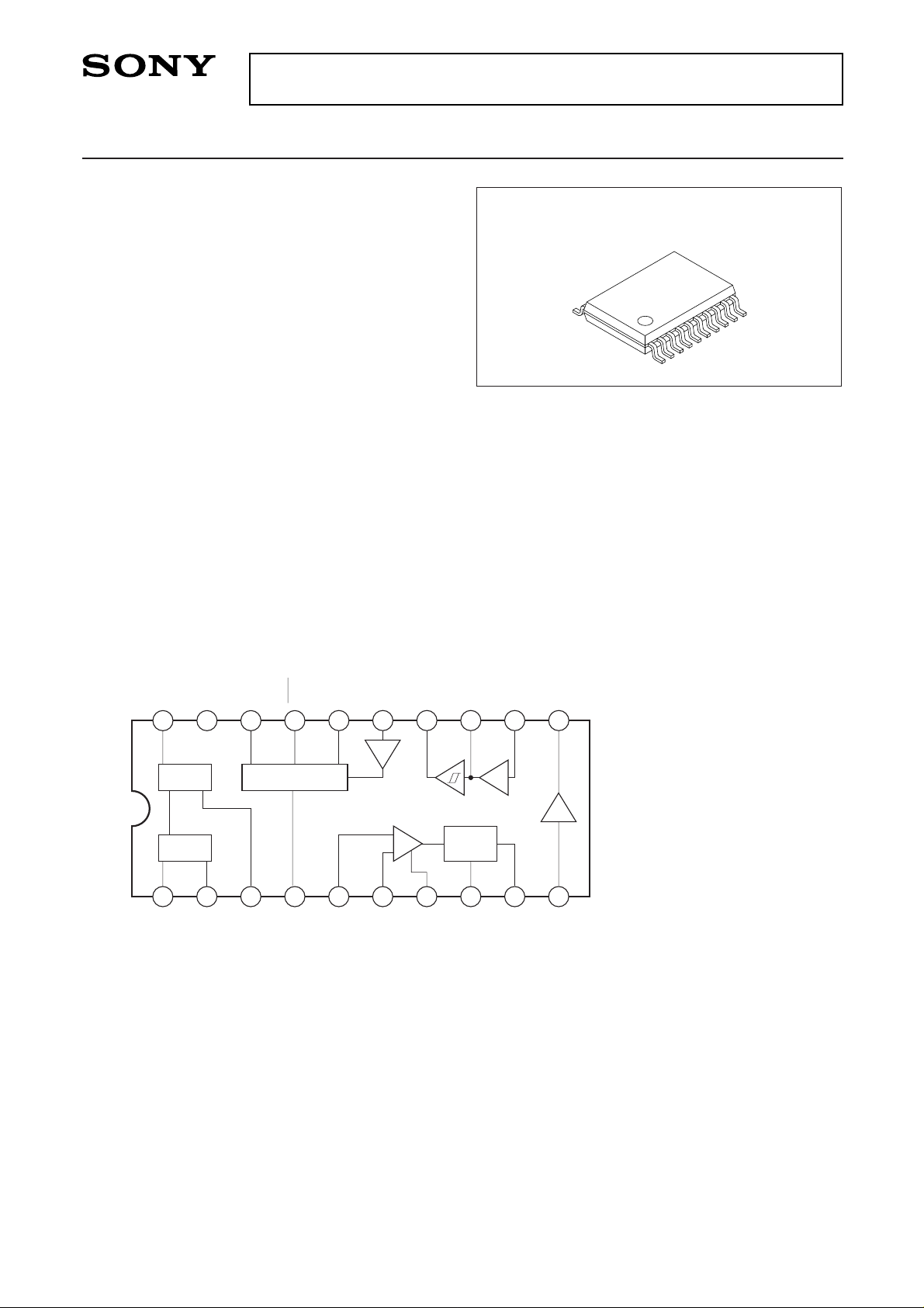
Block Diagram and Pin Configuration
Absolute Maximum Ratings (Ta = 25°C)
• Supply voltage Vcc 7 V
• Operating temperature Topr –20 to +75 °C
• Storage temperature Tstg –65 to +150 °C
Recommended Operating Conditions
Supply voltage Vcc 1.0 to 4.0 V
– 1 –
E97Z05A8Y
Sony reserves the right to change products and specifications without prior notice. This information does not convey any license by
any implication or otherwise under any patents or other right. Application circuits shown, if any, are typical examples illustrating the
operation of the devices. Sony cannot assume responsibility for any problems arising out of the use of these circuits.
CXA1884N
20 pin SSOP (Plastic)
RF IN
OSC1
GND
OSC2
LVA
MIX OUT
BSV
V
CC
VB OUT
IF IN
SENSE
IF P1
NRZ
IF P2
COMP IN
QD
A2 IN
DET OUT
A1 OUT
A1 IN
MIXER
OSC
QUAD
DET.
A2
ERR.
AMP
REG.
IF LIM.
A1
2
3
4
5
6
7
8
9
10
1
11
16
17
18
19
20
12
13
14
15
Note) DET. : DETECTOR
LIM. : LIMITER
REG. :REGURATOR
ERR. : ERROR CORRECTION
– 2 –
CXA1884N
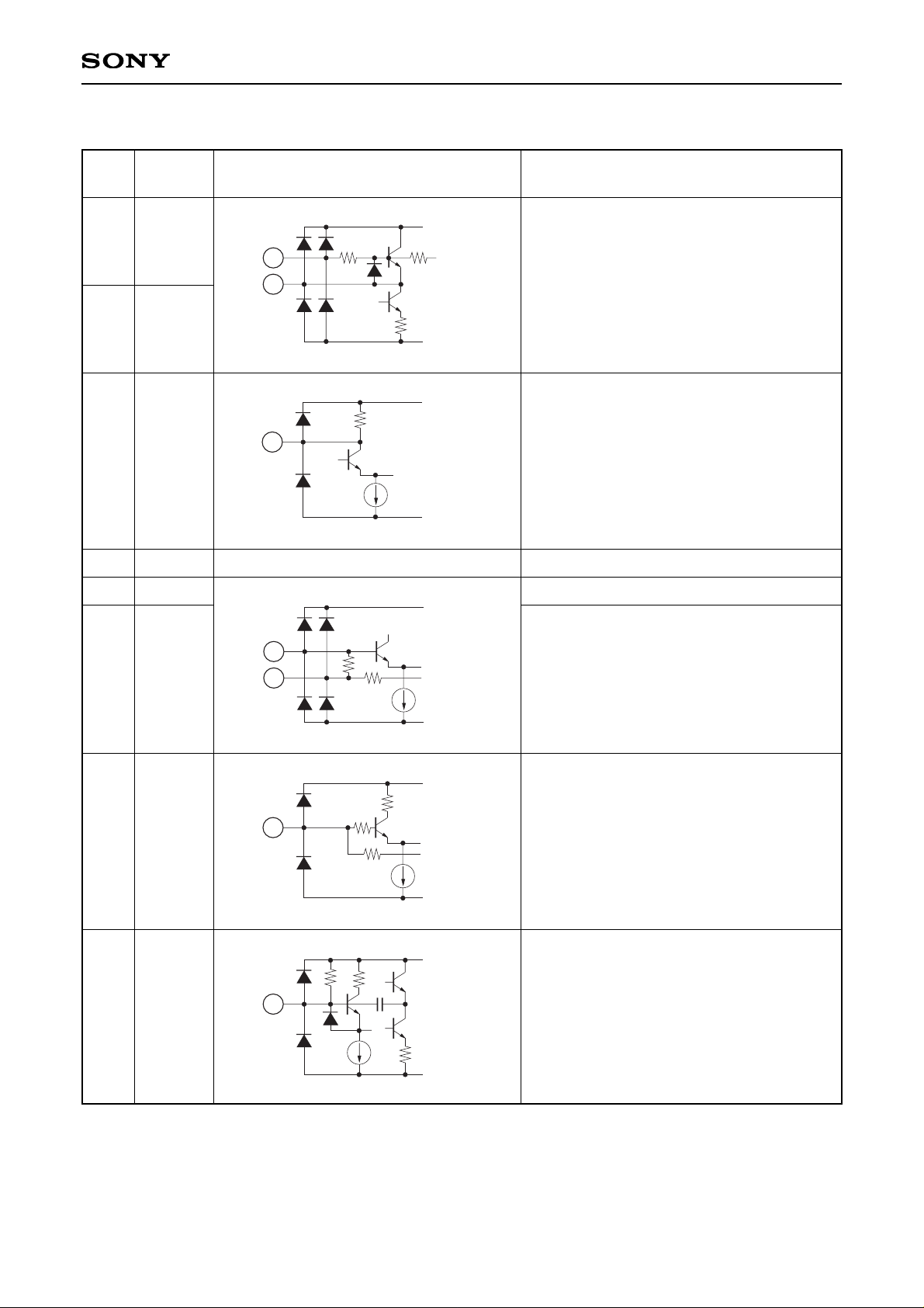
Pin Description
Pin
No.
1 OSC1
Those pins are connected to the external
parts of an oscillating circuit.
The oscillator is an internally-biased Colpitts
type with the collector, base, and emitter
connections at Vcc, pins 1 and 2
respectively.
Mixer output pin. Connect a 455kHz ceramic
filter between this pin and the IF IN pin.
Vcc pin.
Input pin for the IF limiter amplifier.
Connection pin of the bypass capacitor for
the IF limiter amplifier. Connect a capacitor of
about 0.047µF between this pin and ground
(or Vcc).
Connection pin of the bypass capacitor for
the IF limiter amplifier. Connect a capacitor of
about 0.047µF between this pin and ground
(or Vcc).
Connected to a quadrature detector phase
shifter.
OSC2
MIX OUT
VCC
IF IN
IF P1
IF P2
QD
2
3
4
5
6
7
8
Symbol Equivalent circuit Description
VCC
GND
2
1
VCC
GND
3
VCC
GND
5
6
VCC
GND
7
VCC
GND
8
– 3 –
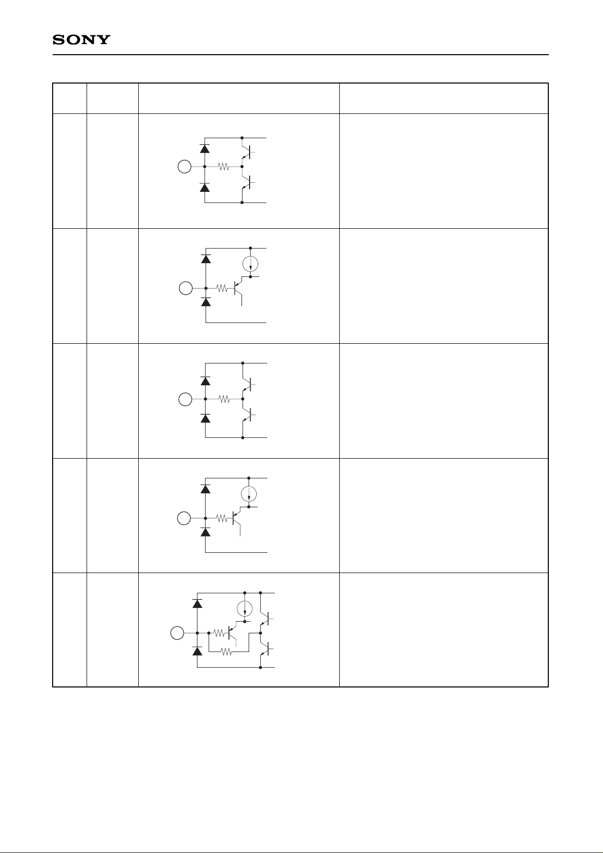
CXA1884N
Pin
No.
9
DET OUT
Recovered signal output.
Symbol Equivalent circuit Description
9
VCC
GND
10
A1 IN
Input pin of inverting OP amplifier A1.
VCC
GND
10
11
A1 OUT
Output pin of OP amplifier A1.
VCC
GND
11
12
A2 IN
Input pin of OP amplifier A2.
VCC
GND
12
13
COMP
IN
Input pin of the comparator.
This pin is internally connected to the output
of OP amplifier A2.
VCC
GND
13

– 4 –
CXA1884N
Pin
No.
15
SENSE
Voltage control pin for external bias supply.
Symbol Equivalent circuit Description
VCC
GND
15
16
VB OUT
Supplies bias voltage to external circuit
transistors and others.
VCC
GND
16
20
RF IN
Mixer input pin.
20
VCC
GND
17
BSV
Reduces IC power consumption.
Lowering pin voltage beiow 0.35V stops IC
operation.
GND
17
18
LVA
Output pin for Low Voltage Alarm (LVA).
The pin turns to high impedance when
power voltage drops below 1.05V.
18
GND
19
GND
Ground pin.
14 NRZ
NRZ (Non Return Zero) output pin.
GND
14
– 5 –
CXA1884N
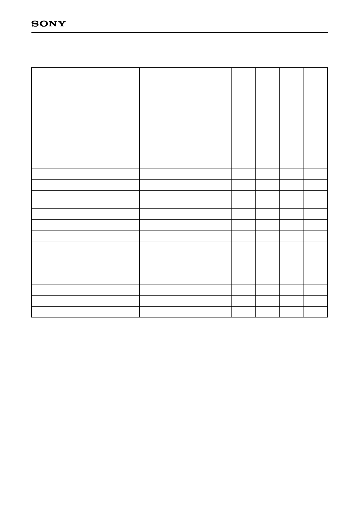
Electrical Characteristics
(VCC = 1.5V, Ta = 25°C, fs = 21.7MHz, fMOD = 256Hz, fDIV = 2.3kHz, AMMOD = 30%)
Item
Power consumption (during operation)
Power consumption
(during battery saving)
Input for –3dB Limiting
AM rejection ratio
OP amplifier input bias current
OP amplifier open loop gain
OP amplifier output voltage amplitude
Comparator hysteresis width
NRZ∗output leak current
NRZ∗saturation voltage
VB output current
VB output voltage
Sense voltage
LVA threshold voltage
LVA hysteresis width
LVA output leak current
LVA saturation voltage
Recovered signal voltage
BSV high level
BSV low level
ICC
ICCS
VIN (LIM)
AMRR
IBIAS
AV
VO
VTW
ILNRZ
VSATNRZ
IOUT
VBOUT
VSEN
VPML
VPMTH
ILLVA
VSATLVA
VDET
VTHBSV
VTLBSV
Test circuit 1
Test circuit 1
VI = 0.3V
Test circuit 3
VIN = 60dBµ
Test circuit 3
Test circuit 2
Test ciTcuit 4
Test circuit 5
Test circuit 6
Test circuit 7
ISINK = 200µA
Test circuit 8
VB = 0.9V
Test circuit 9
Test circuit 2
Test circuit 10
VPMH – VPML
Test circuit 7
Test circuit 8
Test circuit 3
1.2
—
—
25
—
45
0.25
30
—
—
0.1
0.95
85
1.00
35
—
—
10
0.95
—
2.0
—
7
—
30
60
—
40
—
—
—
—
100
1.05
50
—
—
—
—
—
2.6
20
—
—
100
—
—
50
5.0
0.4
—
—
115
1.10
70
5.0
0.4
—
—
0.35
mA
µA
dBµ
dB
nA
dB
Vp-p
mV
µA
V
mA
V
mV
V
mV
µA
V
mVrms
V
V
Symbol Condition Min. Typ. Max. Unit
∗
NRZ: Non Return Zero
 Loading...