

Sony CXA1875AP, CXA1875AM Datasheet

—1—
E94X27-TE
Sony reserves the right to change products and specifications without prior notice. This information does not convey any license by
any implication or otherwise under any patents or other right. Application circuits shown, if any, are typical examples illustrating the
operation of the devices. Sony cannot assume responsibility for any problems arising out of the use of these circuits.
Absolute Maximum Ratings (Ta=25°C)
• Supply voltage VCC 7V
•Operating temperature Topr –20 to +75 °C
• Storage temperature Tstg –65 to +150 °C
• Allowable power dissipation
PD 960 mW
Operating Conditions
• Supply voltage VCC 5±0.5 V
• Operating temperature Topr –20 to +75 °C
Description
The CXA1875AP/AM is developed as a 8-bit 5 ch
D/A converter compatible with I2C bus.
Features
• Serial control through I2C bus
• 4 built-in general purpose I/O ports (Digital I/O)
• I/O can be specified to respective ports
independently
• Selection of 8 slave addresses possible through
address select pins (3 pins)
Applications
I2C bus can control ICs that do not correspond to
I2C bus by connecting the DC control pins of them.
Structure
Bipolar silicon monolithic IC
8-bit D/A Converter Compatible with I2C Bus
CXA1875AP/AM
16 pin DIP (Plastic) 16 pin SOP (Plastic)

—2—
CXA1875AP/AM
Pin Configuration (Top View)
Block Diagram
16 15 14 13 12
9
1011
3 4 5 6 7 821
SW1 SW0 DAC4 DAC3 DAC2 DAC1 DAC0 GND
V
CC SCL SDA SAD2 SAD1 SAD0 SW3 SW2
I
2
C bus
Slave address select pin SW I/O
SW I/O DAC output
SAD2 SAD1 SAD0
LATCH
DAC
AMP
DAC4
LATCH
DAC
AMP
DAC3
LATCH
DAC
AMP
DAC2
LATCH
DAC
AMP
DAC1
LATCH
DAC
AMP
DAC0
VCC
Power
on
Reset
Level
Conversion
I
2
C BUS
SDA
SCL
Level
Conversion
LATCH
Level
Conversion
SW0-3
Open collector
I
2
C Decoder
V
CC
REG
GND
—3—
CXA1875AP/AM
Pin Description
Electrical Characteristics (Ta=25 °C, VCC=5 V)
D/A Converter Block
No. Item Symbol
Test
Test contents Min. Typ. Max. Unit
circuit
6 9 12 mA1 Circuit current ICC 1 DAC 0 to 4=127
–1 0 +1 LSB
0.1 0.4 0.7 V
4.3 4.6 4.9 V
–1 +1 mA
0 3 6 Ω
2
3
4
5
6
Differential
linearity
Minimum output
voltage
Maximum
output voltage
Output current
Output
impedance
DLE
Vmin
Vmax
Iout
Z0
1
1
1
2
2
V(DAC0 to 4=n+1)–V(DAC0 to 4=N)
×128–1
V(DAC0 to 4=191)–V(DAC0 to 4=63)
n=0 to 127
DAC 0 to 4=0
DAC 0 to 4=255
Current that can be flowed from Pins 3
to 7
DAC 0 to 4=127,
V(–1 mA) –V(1 mA)
2 mA
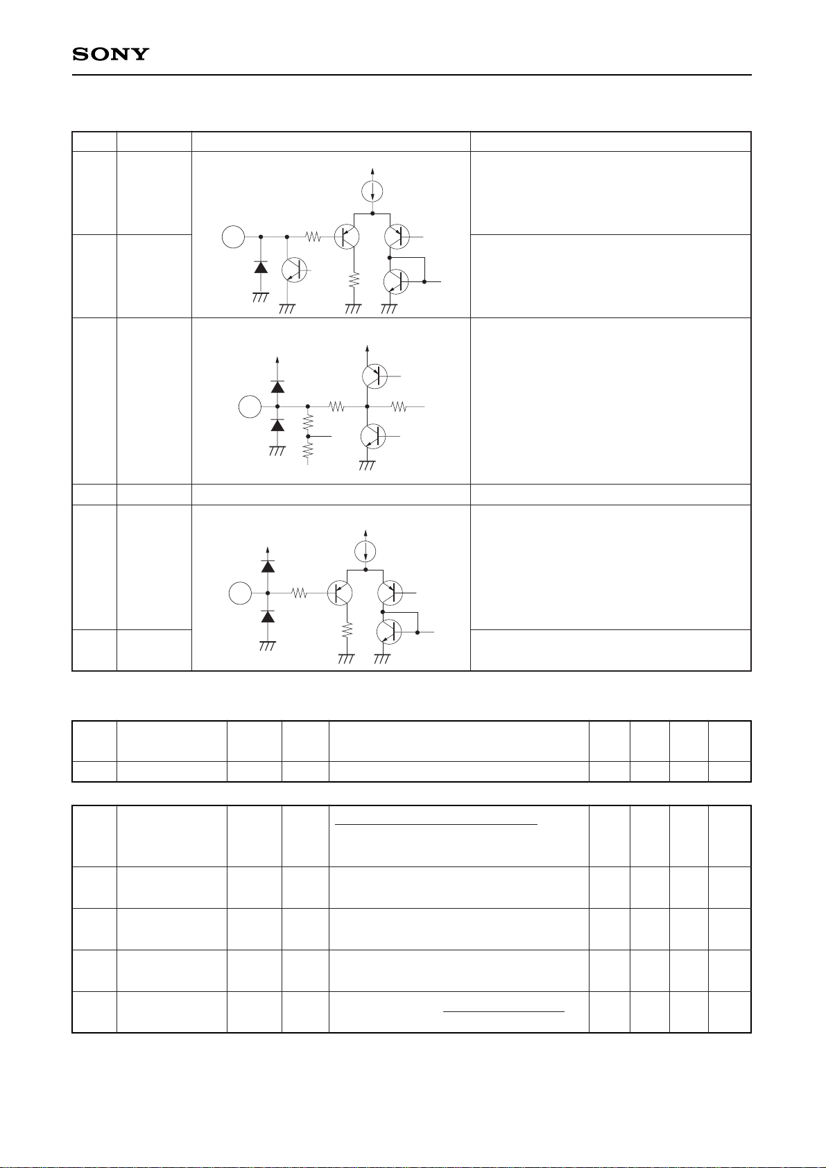
No. Symbol Equivalent circuit Description
I/O pin for general purpose I/O port
VILmax: 1.5 V
VIHmin: 3 V
VOLmax: 0.4 V
SDA I/O pin for I2C bus
D/A converter output pin
GND pin
Slave address input pin
Input at positive logic
VILmax: 1.5 V
VIHmin: 3 V
Power supply pin
VCC
150
4.5k
VCC
56
VCC
20k
20k
22k
VCC
150
4.5k
VCC
1
2
9
10
14
15
3
4
5
6
7
8
11
12
13
16
SW1
SW0
SW2
SW3
SDA
SCL
DAC4
DAC3
DAC2
DAC1
DAC0
GND
SAD0
SAD1
SAD2
VCC
 Loading...