

Sony CXA1870S Datasheet
—1—
E95431-TE
Sony reserves the right to change products and specifications without prior notice. This information does not convey any license by
any implication or otherwise under any patents or other right. Application circuits shown, if any, are typical examples illustrating the
operation of the devices. Sony cannot assume responsibility for any problems arising out of the use of these circuits.
Absolute Maximum Ratings (Ta=25 °C)
• Supply voltage VCC 12 V
• Operating temperature Topr –20 to +75 °C
• Storage temperature Tstg –65 to +150 °C
• Allowable power dissipation
PD 1.73 W
Recommended Operating Conditions
Supply voltage VCC 9±0.5 V
Description
The CXA1870S is a bipolar IC which integrates the
NTSC color TV luminance signal processing,
chroma signal processing, sync signal processing,
and RGB signal processing onto a single chip.
Features
• I2C bus compatible. Various types of adjustments
and user controls performed with two bus lines
SCL and SDA.
• H and V oscillation frequencies made non-
adjusting with a countdown system.
• Non-adjusting Y system filters (chroma trap, delay
line)
• Built-in V picture distortion correction circuit
• Built-in delay line aperture compensation
• Auto cut-off function for automatic CRT cut-off
adjustment and compensation for changes with
time
• Multiple inputs
Composite video: 2 systems
(Built-in 2-input, 1-output video switch)
Y/C separation input: 1 system
On screen display input: 1 system
Applications
• Color TV
Structure
Bipolar silicon monolithic IC
Color TV Y/C/Jungle
42 pin SDIP (Plastic)
CXA1870S
For the availability of this product, please contact the sales office.
—2—
CXA1870S
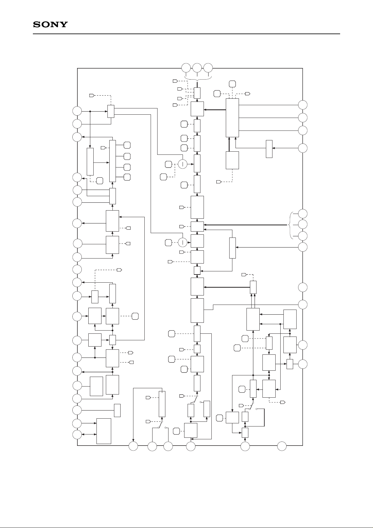
Block Diagram
COLOR
2f
H
ABL
H PHASE
BOUTGOUTROUT
Y IN
V1 IN V2 IN
C IN
V
CC
TRAP SW
TOT SW
COLOR
SUB HUE
OSD
DRIVE
G DRIVE
B DRIVE
IK
G CUTOFF
B CUTOFF
DC TRAN
SHARPNESS
AFC HLOCK
NR
REF
GAMMA
GAMMA
C MODE
HV COMP
V SHIFT
V SIZE
V LIN
S CORR
V OFF
ABL
PMUTE
R OFF
G OFF
B OFF
SCL
SDA
IREF
H SYNC
REG
AFC
CERA
XRAY
HD
J GND
V SYNC
V PLS
VOSC
VD
ABL IN
ABL LPF
V LPF
V HOLD
HP
H S/S OUT
V BIAS
PICTURE
BRIGHT
BRIGHT
SUB BRIGHT
DY COL
AXIS
HUE
SUB COLOR
PRE OVER
BLUE
BLACK
APC
X'TAL
A PED
V GND
IK
R S/H
G S/H
B S/H
OSD
BLK
OSD R
OSD G
OSD B
XRAY
LIMIT
RGB LIM
KILLER
I
2
C BUS
DECODER
IREF
REGU
LATOR
H.SYNC
SEP
PHASE
DET.
32fHVCO
1/32
PHASE
DET
PHASE
SHIFT
H.DRIVE
XRAY
VEX
V.SYNC
SEP
V COUNT
DOWN
VOSC
V COMPENSATION
V ZOOMING
BLK
16
18
20
DC
SHIFT
DYNAMIC
COLOR
OSD
MIX
PIC
TURE
RGB
SW
YM
Y/C MIX
CLAMP
AUTO
PEDESTAL
CLAMP
NR
SHARP
NESS
DELAY
TRAP
BUS
CONT
SUB CONT
0/6DB AMP
SW
GAIN
IN
SW
DELAY
AKB
AKB
TIMING
CLAMP
OSD BLK
AXIS
CHROMA
DET.
PHASE
SHIFT
3.58M
VCO
LPF
HUE
12
13
14
10
19
17
15
11
21
8
1
2
PHASE
DET.
COLOR
KILLER
TOT
ACC
ACC
DET.
3
7
4
6
22
9
31
29
32
26
24
25
23
38
37
36
35
40
34
39
33
30
41
5
27
42
28
SW OUT

—3—
CXA1870S
Pin Configuration
V2 IN
V BIAS
SDA
SCL
V SYNC
H SYNC
H S/S OUT
REG
IREF
AFC
CERA
J GND
HP
XRAY
HD
V PLS
V LPF
V OSC
ABL LPF
VD
ABL IN
X'TAL
V
CC
APC
V1 IN
A PED
Y IN
C IN
V GND
OSD BLK
OSD R
OSD G
OSD B
R S/H
R OUT
G S/H
G OUT
B S/H
B OUT
IK
V HOLD
SW OUT
1
2
3
4
5
6
7
8
9
10
11
12
13
14
15
16
17
18
19
20
21 22
23
24
25
26
27
29
30
31
32
33
35
36
37
38
39
40
41
42
28
34
—4—
CXA1870S
Pin Description
Pin
No.
1
2
3
4
22
5
Symbol
X'TAL
APC
VCC
V1 IN
V2 IN
V HOLD
Pin
voltage
2.6 V
5 V
9 V
2 V
0.7 V
Description
Connect a 3.58 MHz crystal
oscillator.
APC lag-lead filter CR connection
pin.
Power supply pin.
Video switch input pins. Sync tip
clamping is performed, so input
via capacitors.
Peak hold pin for V sync
separation. Connect a capacitor.
500
4k
1
VCC
1.2k
25k
1.2k
2
VCC
VCC
150
1k
55k
50k
5
VCC
150
4
22
VCC
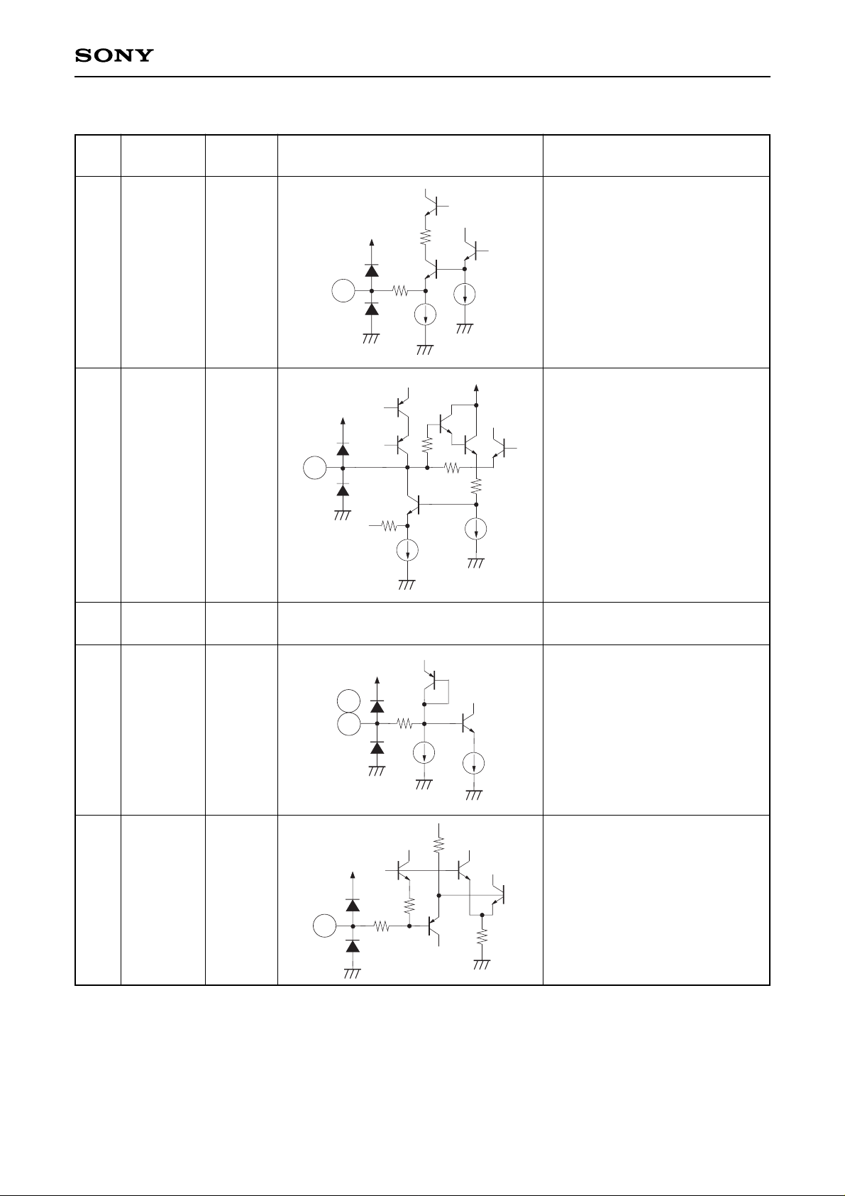
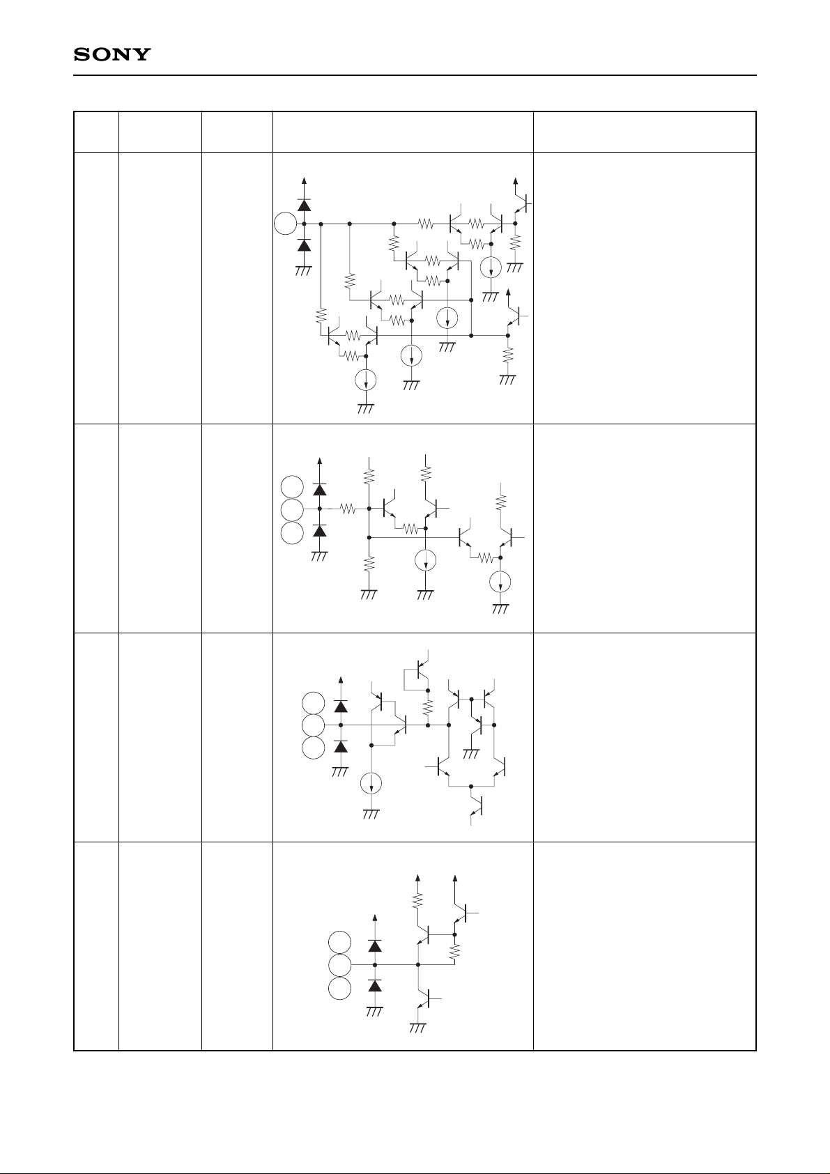
Equivalent circuit
—5—
CXA1870S
Pin
No.
6
7
8
9
10
Symbol
SW OUT
Y IN
A PED
C IN
V GND
Pin
voltage
—
3.5 V
3.5 V
—
—
Description
Video switch output pin.
Y signal input pin. Input via a
capacitor.
Standard input level: 2 Vp-p
Auto pedestal (black elongation)
black peak hold pin. Connect a
capacitor.
Chroma signal input pin.
Standard input level (burst level):
570 mVp-p
Video system (Y/C/RGB) GND
pin.
2k
30k
12k
25k
500
6
VCC
VCC VCC
50k
1.2k
7
VCC
VCC
6k
6k
30k
30k
9
VCC
16k
20k
20k
1.2k
8
VCC
VCC VCC VCC
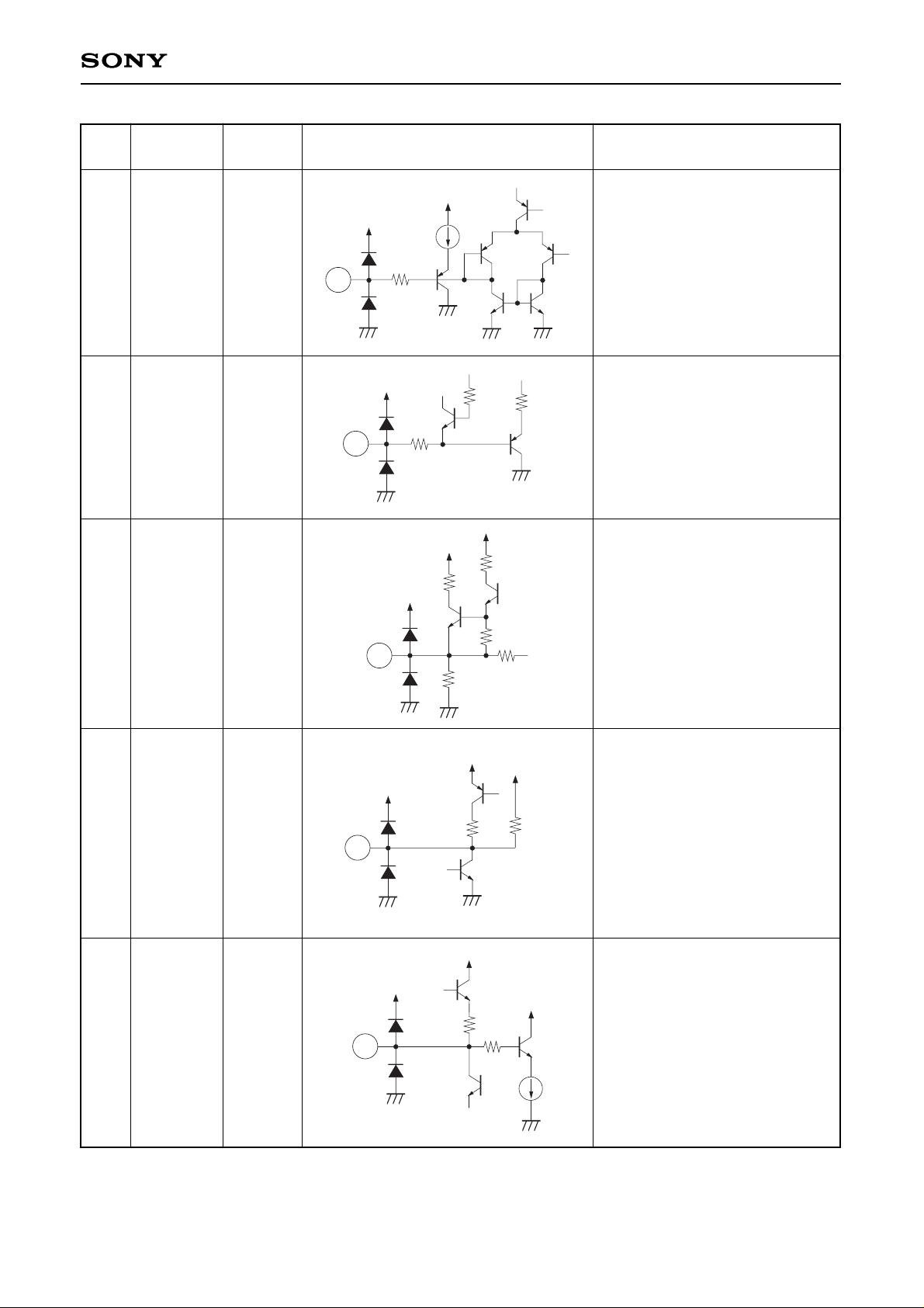
Equivalent circuit
—6—
CXA1870S
Pin
No.
11
12
13
14
15
17
19
16
18
20
Symbol
OSD BLK
OSD R
OSD G
OSD B
R S/H
G S/H
B S/H
R OUT
G OUT
B OUT
Pin
voltage
—
—
—
—
Description
Blanking signal input pin for OSD
RGB input.
0 to 1 V: Blanking not performed.
2 to 3 V: Signal from Y IN/C IN
lowered by –6 dB.
4 to 6 V: R, G and B outputs
become lower than
black level.
Digital R, G and B signal input
pins for on screen display.
0 to 1 V: No OSD display.
2 to 3 V: OSD level = 46 IRE
(33 IRE)
4 to 6 V: OSD level = 92 IRE
(65 IRE)
Figures in parentheses are for
when the I2C OSD register is set
to 0.
Sample-and-hold pins for R, G
and B AKB (Auto Kinetic Bias).
Connect to GND via capacitors.
R, G and B output pins.
40k
15k
2k
60k
30k
2k60k
30k
2k
60k
11
30k
2k
VCC
VCC
VCC
12
13
14
VCC
1.2k
15
17
19
VCC
150
5k
16
18
20
VCC
VCC VCC
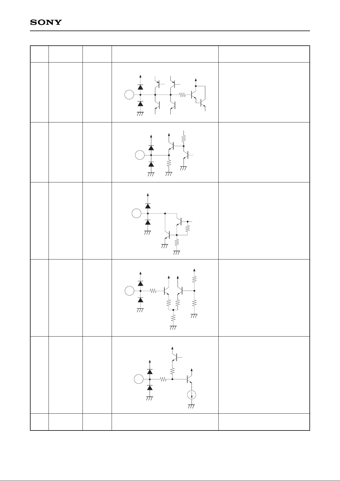
Equivalent circuit
—7—
CXA1870S
Pin
No.
21
23
24
25
26
Symbol
IK
ABL IN
VD
ABL LPF
V OSC
Description
Inputs the signal obtained by
converting the CRT beam current
(Ik) into voltage. Connect to an
emitter follower via a capacitor.
ABL voltage input pin.
Vertical deflection sawtooth wave
output pin.
ABL signal LPF pin.
Connect a capacitor.
Connect a capacitor to generate
the V sawtooth wave.
150
21
V
CC
VCC
150
10k
30k
23
V
CC
5k
3k
3k
15k
24k
24
VCC
VCC
VCC
24k
100k
25
VCC
VCC
VCC
100
100
26
VCC
VCC
VCC
Pin
voltage
—
—
—
—
—
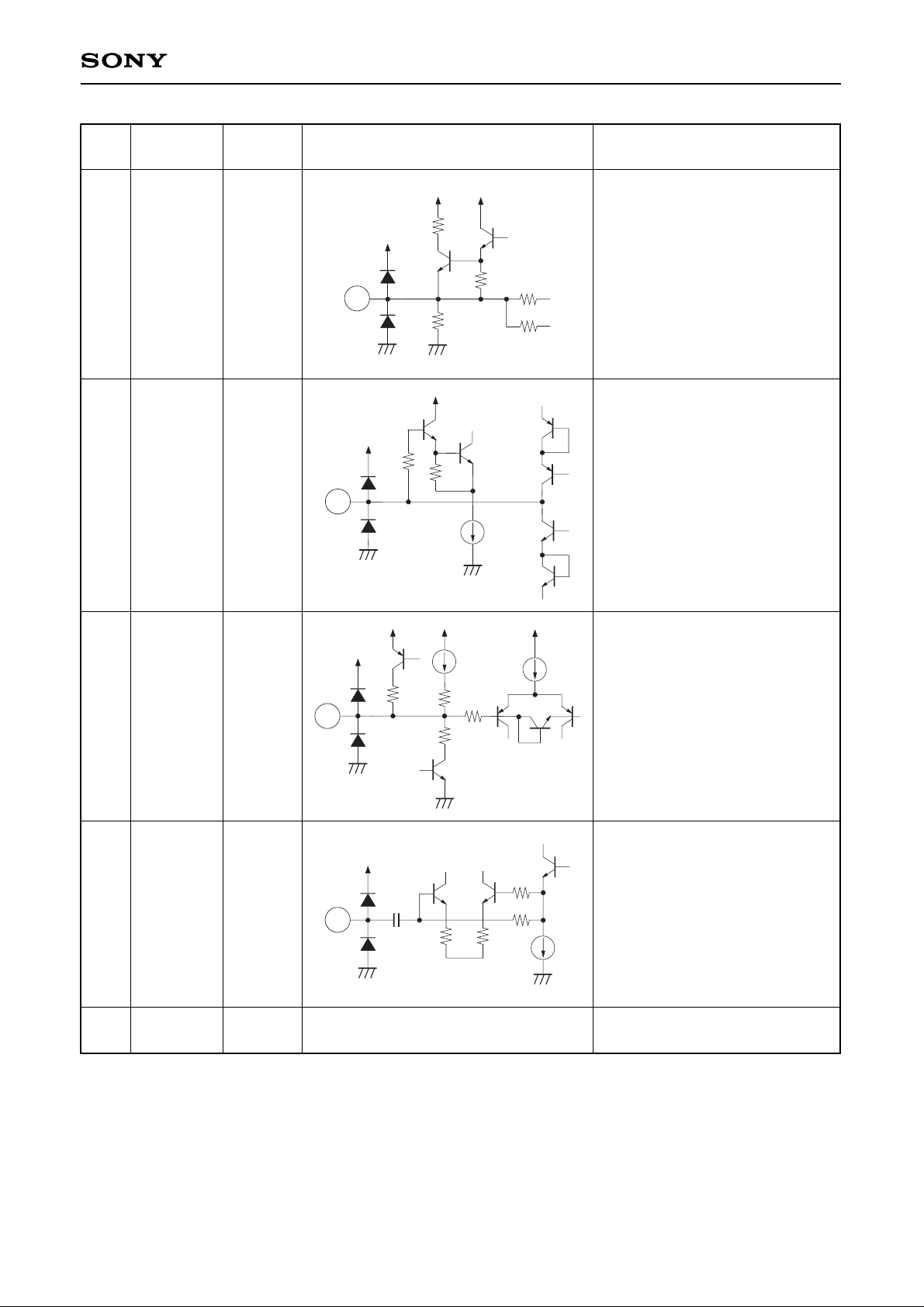
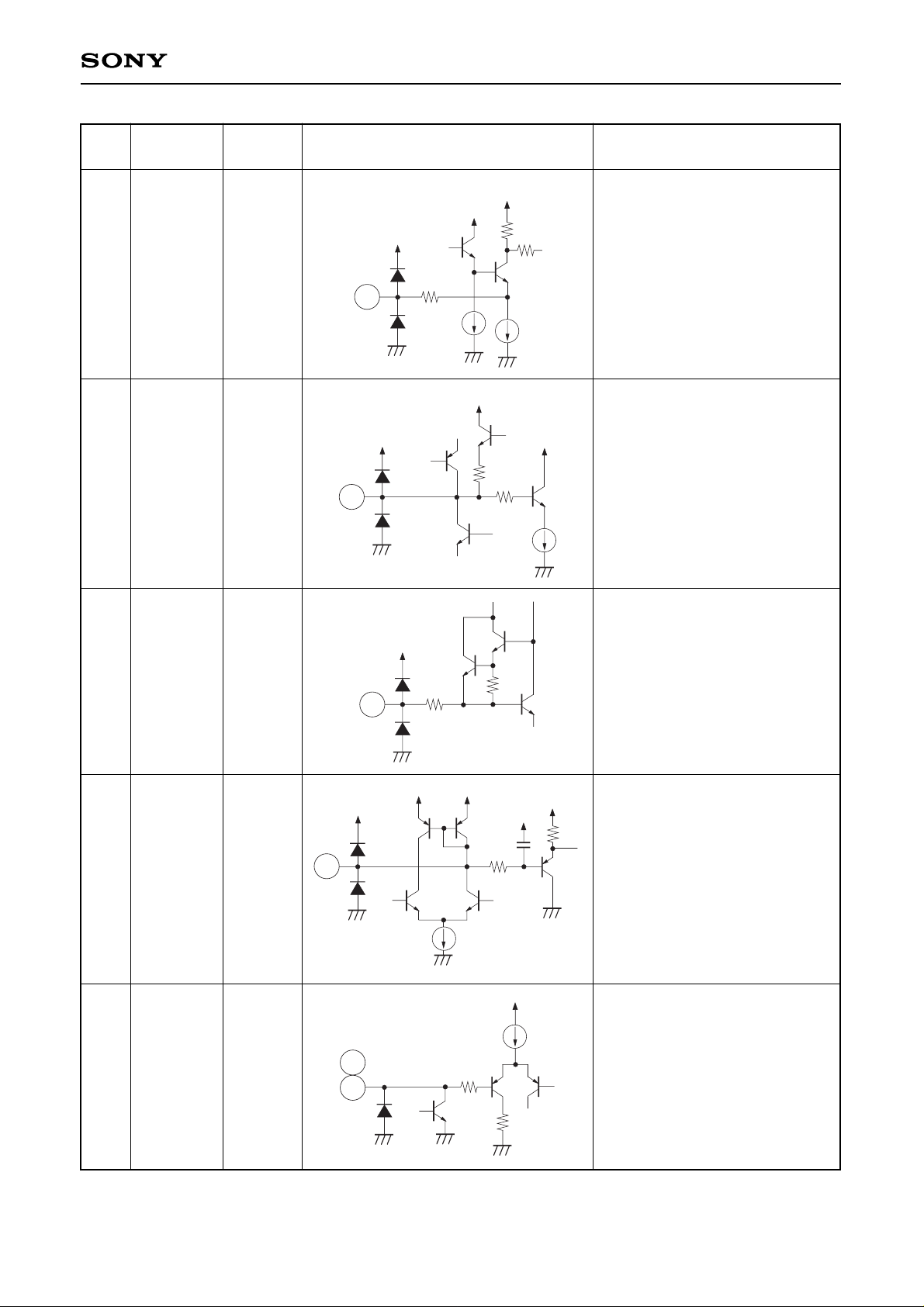
Equivalent circuit
—8—
CXA1870S
Pin
No.
27
28
29
30
31
32
Symbol
V LPF
V PLS
HD
XRAY
HP
J GND
Description
Connect a capacitor to hold the
AGC voltage which maintains the
V sawtooth wave at a constant
amplitude.
V pulse output pin. A negative
polarity pulse 3 to 3.5 H width is
output from this pin.
High level: 4.5 V
Low level: 0 V
H drive output pin. This pin is
output at the open collector.
X-ray protection circuit input pin.
When a pulse with a width of 7 V
or more is input, HD output
becomes low and R, G and B
outputs are blanked. This status
is maintained until the power
supply is turned off.
Vilmax = 2.4 V
Vihmin = 3.0 V
H pulse input pin. Inputs a 3 to 5
Vp-p signal via a capacitor.
Jungle system (H/V) GND pin.
VCC
27
VCC
VCC
20k
20k
29
19k
30k
40k
30k
63k
27k
30
VCC
VCC VCC
VCC
VCC
10k
60k
V
CC
VCC
31
74k
18k
28
VCC
VCC
Pin
voltage
5 V
—
—
—
3.3 V
(at no
signal)
—
Equivalent circuit
—9—
CXA1870S
Pin
No.
33
34
35
36
37
38
Symbol
CERA
AFC
IREF
REG
SCL
SDA
Description
Connect a 32 fh (503.5 kHz)
ceramic oscillator.
AFC lag-lead filter CR connection
pin.
Connect a 15 kΩ resistor between
this pin and GND.
Regulator pin for voltage
generated internally from VCC.
Connect a capacitor for
stabilization.
I2C bus SCL (Serial Clock) and
SDA (Serial Data) pins.
Vilmax = 1.5 V
Vihmin = 3 V
Volmax = 0.4 V
VCC
10k
28k
V
CC
VCC
330
33
VCC
40k
1.2k
V
CC
VCC
34
150
20k
35
VCC
1.2k
40k
4p
36
50µA
VCC
VCC
VCC
VCC
VCC
4k
4k
37
38
VCC
Pin
voltage
2.3 V
3.2 V
2.6 V
7 V
—
Equivalent circuit

—10—
CXA1870S
Pin
No.
39
40
41
42
Symbol
H S/S OUT
H SYNC
V SYNC
V BIAS
Description
H sync separation pulse output.
A positive polarity pulse is output
from this pin.
High level: 4.6 V
Low level: 0 V
H sync separation input pin.
Inputs a 2 Vp-p video signal via a
capacitor and resistor.
V sync separation input pin.
Inputs a 2 Vp-p video signal via a
capacitor and resistor.
The V oscillator reference voltage
is output from this pin.
23k
1.2k
39
V
CC
VCC
150
14k
24k
20k
40
10µA
V
CC
VCC
150
10k
26k
31k
10k
20k
41
20µA
30k
4k
20k
42
V
CC
VCC
Pin
voltage
—
2.6 V
3.4 V
3.8 V
Equivalent circuit
—11—
CXA1870S
Electrical Characteristics
Setting conditions
• Ta = 25 °C VCC = 9 V
• I2C bus register should be set to “I2C Bus Register Initial Settings”.
Measurement
conditions
Video In: Sig-H2,H3
AFC: 0
Video In: Sig-H6
AFC: 0
Video In: Sig-H7
AFC: 0
Video In: Sig-H6
AFC: 1
Video In: Sig-H7
AFC: 1
Video In: Sig-H6
AFC: 2
Video In: Sig-H7
AFC: 2
Video In: Sig-H1
Video In: Sig-H1
Video In: Sig-H1
Video In: Sig-Y11
HPHASE: F
Video In: Sig-Y11
HPHASE: 7
Video In: Sig-Y11
HPHASE: 0
Video In: Sig-Y11
No.
2
3
4
5
6
7
8
9
10
11
12
13
14
15
16
17
Item
Horizontal free
running frequency
Horizontal sync
pull-in range
AFC gain 1
AFC gain 2
AFC gain 3
HD output pulse
width
HD output
high level
HD output
low level
Horizontal phase
operating range 1
Horizontal phase
operating range 2
Horizontal phase
operating range 3
HP blanking
delay time 1
HP blanking
delay time 2
HSS OUT
high level
HSS OUT
low level
Overvoltage
protection circuit VHT
H system items
Symbol
Hfree
∆H
AFCmax
AFCcen
AFCmin
HD, W
HD, H
HD, L
HPHmax
HPHcen
HPHmin
HPBLK1
HPBLK2
HSS, H
HSS, L
XVTH
Measurement method
Check that I2C register HLOCK is 1.
AFCmax=t1-t2
AFCcen=t1-t2
AFCmin=t1-t2
t1: Video In: Time from
fall of Sig-H6 to rise of
Pin 31.
t2: Video In: Time from
fall of Sig-H7 to rise of
Pin 31.
Check that HD appears at 2.4 V and
disappears at 2.8 V.
Measurement
pin
29
31
31
31
29
20
31
20
31
39
30
HSS,H
HSS,L
HPBLK1
HPBLK2
Pin 20
Pin 31
HPH
Pin 20
Pin 31
HD,H
HD,L
HD,W
No.
1
Item
Current
consumption 1
Symbol
ICC1
Measurement
conditions
Measurement
pin
3
Measurement method
Measure the VCC pin inflow current.
Min.53Typ.80Max.
110
Unit
mA
Min.
15.60
–400
0.12
—
0.75
24
8.7
0.5
–4.3
–1.5
1.3
—
—
4
0
2.4
Typ.
15.78
—
0.3
0.5
1.2
26
9
0.8
–3.3
–0.5
2.3
100
100
4.6
0.1
2.6
Max.
15.96
400
0.48
—
1.75
28
—
1.1
–2.3
0.5
3.3
—
—
5
0.5
2.8
Unit
kHz
µs
µs
µs
µs
µs
V
V
µs
µs
µs
ns
ns
V
V
V

—12—
CXA1870S
V system items
Measurement
conditions
Video In: Sig-V1
V SHIFT: F
V SHIFT: 0
V SHIFT: 1F
V SIZE: 0
V SIZE: 3F
S CORR: 0
S CORR: F
V LIN: 0
V LIN: F
HV COMP: 0,
Pin 23: 6 V
HV COMP: 7,
Pin 23: 6 V
HV COMP: 0,
Pin 23: 0 V
HV COMP: 7,
Pin 23: 0 V
Item
VBias
V PLS high level
V PLS low level
VD output
center voltage
V SHIFT variable
range 1
V SHIFT variable
range 2
V SIZE variable
range 1
V SIZE variable
range 2
S CORR variable
range 1
S CORR variable
range 2
V LIN variable
range 1
V LIN variable
range 2
V zooming 1
V zooming 2
Symbol
V
Bias
VPLS, H
VPLS, L
VDcen
VSHIFT–
VSHIFT+
VSIZE–
VSIZE+
∆ Sa
∆ Sc
∆ La
∆ Lc
∆VZ1
∆VZ2
Vb
Vb-VDcen
Vb-VDcen
Vc-Va
Vc-Va
Vsa=Va
Vsc=Vc
Va-Vsa
Vc-Vsc
Vla=Va
Vlc=Vc
Va-Vla
Vc-Vlc
Vsmin=
Vc-Va
Vsmax=
Vc-Va
Vsmin(Vc-Va)
Vsmax(Vc-Va)
Measurement
pin
42
28
24
Video
In:
Sig-V1
Vc
Vb
Va
GND
VTRIG
0.1ms
8.75ms
16.57ms
Pin 24
VPLS, L
VPLS, H
Measurement method
Measure the pin voltage.
No.
18
19
20
21
22
23
24
25
26
27
28
29
30
31
Unit
V
V
V
V
mV
mV
V
V
mV
mV
mV
mV
mV
mV
Max.
5
0.5
3.05
–115
140
1.2
1.8
85
–15
140
110
15
100
Typ.
3.8
4.5
0.1
2.9
–125
120
1.1
1.65
65
–35
120
90
3
80
Min.
4
0
2.75
–140
110
0.9
1.5
45
–55
90
60
0
60
 Loading...