

Sony CXA1854AR Datasheet

CXA1854AR
For the availability of this product, please contact the sales office.
Decoder/Driver/Timing Generator for Color LCD Panels
Description
The CXA1854AR is an IC designed exclusively to
drive color LCD panels LCX009AK/AKB/LCX005BK/
BKB. This IC greatly reduces the number of circuits
and parts required to drive LCD panels by
incorporating RGB decoder functions for video
signals, driver functions, and a timing generator for
driving panels onto a single chip.
64 pin LQFP (Plastic)
Features
• Color LCD panels
LCX009AK/AKB/LCX005BK/BKB driver
• Both NTSC/PAL compatible
• Supports composite inputs, Y/C inputs and Y/color
difference inputs
• Band-pass filter, trap and delay line
• Sharpness function
• 2-point γ compensation circuits
• R, B output delay time adjustment circuit
(supports both right and left inversion)
• Polarity reversed circuit / line inverted mode
• Supports external RGB input
• Supports line inversion
• Supports AC drive for LCD panel during no signal
Applications
• Color LCD viewfinders
• Liquid crystal projectors
• Industrial monitors
Structure
Bipolar CMOS IC
Absolute Maximum Ratings (Ta = 25°C)
• Supply voltage VCC1 – GND 6 V
• Supply voltage VCC2 – GND 14 V
• Supply voltage VDD – VSS 6V
•Analog input pin voltage
VINA –0.3 to VCC1V
•Digital input pin voltage
VIND –0.3 to VDD + 0.3 V
• Operating temperature range
Topr –15 to +70 °C
• Storage temperature range
Tstg –40 to +150 °C
• Allowable power dissipation
PD (Ta ≤ 70°C) 400 mW
Operating conditions
• Supply voltage VCC1 – GND 4.6 to 5.3 V
• Supply voltage VCC2 – GND 11.0 to 13.0 V
• Supply voltage
LCX009 mode VDD – VSS 4.5 to 5.5 V
LCX005 mode VDD – VSS 2.7 to 5.5 V
Sony reserves the right to change products and specifications without prior notice. This information does not convey any license by
any implication or otherwise under any patents or other right. Application circuits shown, if any, are typical examples illustrating the
operation of the devices. Sony cannot assume responsibility for any problems arising out of the use of these circuits.
– 1 –
E95X01A73
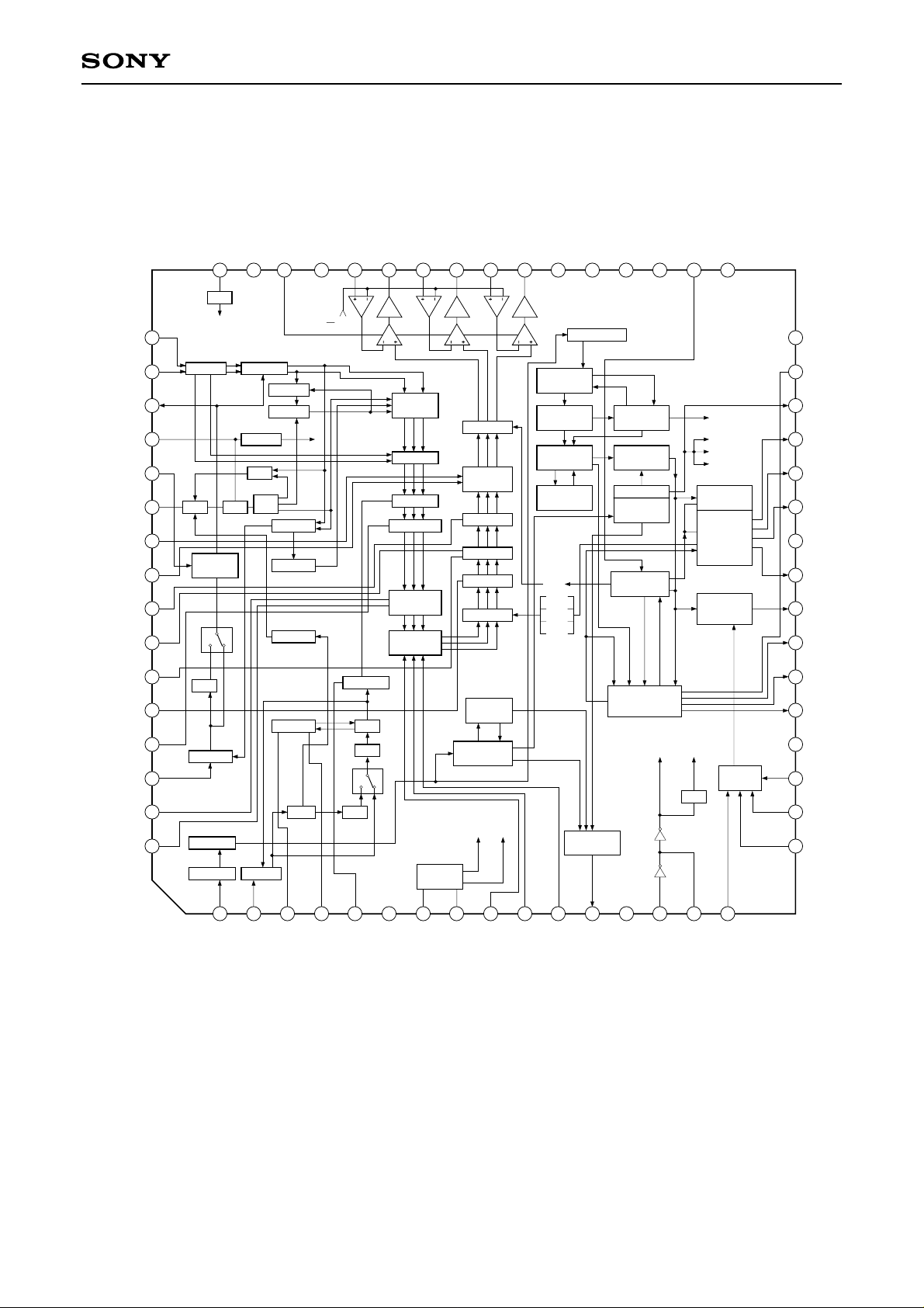
Block Diagram
CXA1854AR
B-YIN
R-YIN
COUT
HUE/RST
COLOR
XVXO
R-BRT
B-BRT
RGB-GAIN
GAMMA2
GAMMA1
BRIGHT
CONTRAST
CIN
R-GAIN
49
50
51
52
53
54
55
56
57
58
59
60
61
62
63
REG
48
REG.
REGV
VXO HUE
COLOR
CONT
BPF
ACC AMP
BLKLIM
46
KILLER
XCLR
2
CC
V
45
1
CC2
V
2
FB B
44
PIC CONT
AGC
DL 2
DL 1TRAP
B OUT
43
DEMOD
LPF
MATRIX
CONTRAST
RGB
SUB
CONTRAST
EXT SW
42
FB G
FB R
G OUT
40
POL SW
SUB
BRIGHT
RGB GAIN
GAMMA
BRIGHT
S/H
HALF-H
KILLER
H-SYNC DET
H-SKEW DET
R OUT
39
bufbufbuf
38
V-POS
RESET GEN
V-CTL
COUNTER
V-CTL
DECODER
AUX-V
COUNTER
FRP
SH1
SH2
SH3
SH4
1
CC
V
47
+5V +12V +5VGND2
INT/EXTCLAMP
PAL ID
PAL SW
RESET
APC
PS
ACC DET
FILT CAL
AGG DET
GND2
37
V-SYNC SEP
TEST8
FIELD & LINE
TEST7
35
36
V-POS
COUNTER
H-CTL
DECODER
DECODER
PLL
COUNTER
CTL
PULSE GEN
V-TIMING
MASTERCKSUB
TEST6
RGT
34
EQP
BGP
CLP
BLK
H-POS
COUNTER
DECODER &
H-TIMING
PULSE GEN
PAL PULSE
ELIM &
MODE SEL
CK
1/7
3341
DD
V
TEST
S/R
TEST5
32
VD
31
HD
30
HCK1
29
HCK2
28
HST1
27
TEST4
26
CLR
25
EN
24
VCK1
23
VCK2
22
VST1
21
TEST3
20
SLCK
19
TEST0
18
B-GAIN
EXT-G
PLL PHASE
11
EXT-B
COMP
12
RPD
TEST1
17
V
SS
13
14
15
SS
CKI
V
CKO
16
TEST2
SYNC SEP
64
YC/YRB/COMP
6
GND1
MODE
SELECT
7
MODE1
8
MODE2
SPAL/DPAL/NTSC
9
10
EXT-R
H. FILTER
1
SYNCIN
CLAMP
2
YIN
3
AGCADJ
4
AGCTC
GND1
5
PICT
– 2 –

CXA1854AR
Pin Description (H: Pull up, M: Intermediate setting, L: Pull down)
Pin
No.
1
2
3
4
5
6
7
8
9
10
11
12
13
14
15
Symbol I/O Description
I
SYNC IN
Y IN
AGCADJ
AGCTC
PICT
GND1
MODE1
MODE2
EXT-R
EXT-G
EXT-B
RPD
VSS
CKI
CKO
Sync input
I
Y signal input
I
AGC level adjustment
O
AGC time constant
I
Y signal frequency characteristics adjustment
Analog 5V GND
I
Switches between NTSC (H), DPAL∗(M) and SPAL∗(L)
I
Switches between composite (H), Y/color difference (M) and YC input (L)
I
External digital input R (input conditions noted separately)
I
External digital input G (input conditions noted separately)
I
External digital input B (input conditions noted separately)
O
Phase comparator output
Digital GND
I
Oscillation cell input
O
Oscillation cell output
Input pin for
open status
M
M
16
17
18
19
20
21
22
23
24
25
26
27
28
29
30
31
32
TEST2
TEST1
TEST0
SLCK
TEST3
VST1
VCK2
VCK1
EN
CLR
TEST4
HST1
HCK2
HCK1
HD
VD
TEST5
I
Test
I
Test
I
Test
I
Switches between LCX005BK (H) and LCX009AK (L)
O
Leave this pin open.
O
V start pulse 1 output
O
V clock pulse 2 output
O
V clock pulse 1 output
O
EN pulse output
O
CLR pulse output
O
Leave this pin open.
O
H start pulse 1 output
O
H clock pulse 2 output
O
H clock pulse 1 output
O
HD pulse output
O
VD pulse output
I
Leave this pin open.
L
L
L
L
L
∗
DPAL supports demodulation methods which use an external delay line during demodulation; SPAL supports
methods which internally process chroma demodulation.
– 3 –
CXA1854AR
Pin
No.
33
34
35
36
37
38
39
40
41
42
43
44
45
46
47
Symbol I/O Description
VDD
RGT
TEST6
TEST7
TEST8
GND2
R OUT
FB R
G OUT
FB G
B OUT
FB B
VCC2
BLKLIM
VCC1
Digital 5V power supply
I
Switches between Normal scan (H) and Reverse scan (L)
I
Leave this pin open.
I
Leave this pin open.
I
Leave this pin open.
Analog 12V GND
O
R output
I
R signal DC voltage feedback input
O
G output
I
G signal DC voltage feedback input
O
B output
I
B signal DC voltage feedback input
Analog 12V power supply
I
Black peak limiter level adjustment
Analog 5V power supply
Input pin for
open status
H
H
H
H
48
49
50
51
52
53
54
55
56
57
58
59
60
61
62
63
64
REG
B-YIN
R-YIN
COUT
HUE/RST
COLOR
XVXO
R-BRT
B-BRT
RGB-GAIN
GAMMA2
GAMMA1
BRIGHT
CONTRAST
CIN
R-GAIN
B-GAIN
O
Constant voltage capacitor connection
I
B-Y demodulator input (or B-Y/color difference signal input)
I
R-Y demodulator input (or R-Y/color difference signal input)
O
Chroma signal output (for PAL 1HDL)
I
Hue adjustment/system reset
I
Color adjustment
I
VXO crystal oscillator connection
I
R brightness adjustment
I
B brightness adjustment
I
RGB gain adjustment
I
γ 2 adjustment
I
γ 1 adjustment
I
Brightness adjustment
I
Contrast adjustment
I
Chroma signal input
I
R gain adjustment
I
B gain adjustment
– 4 –
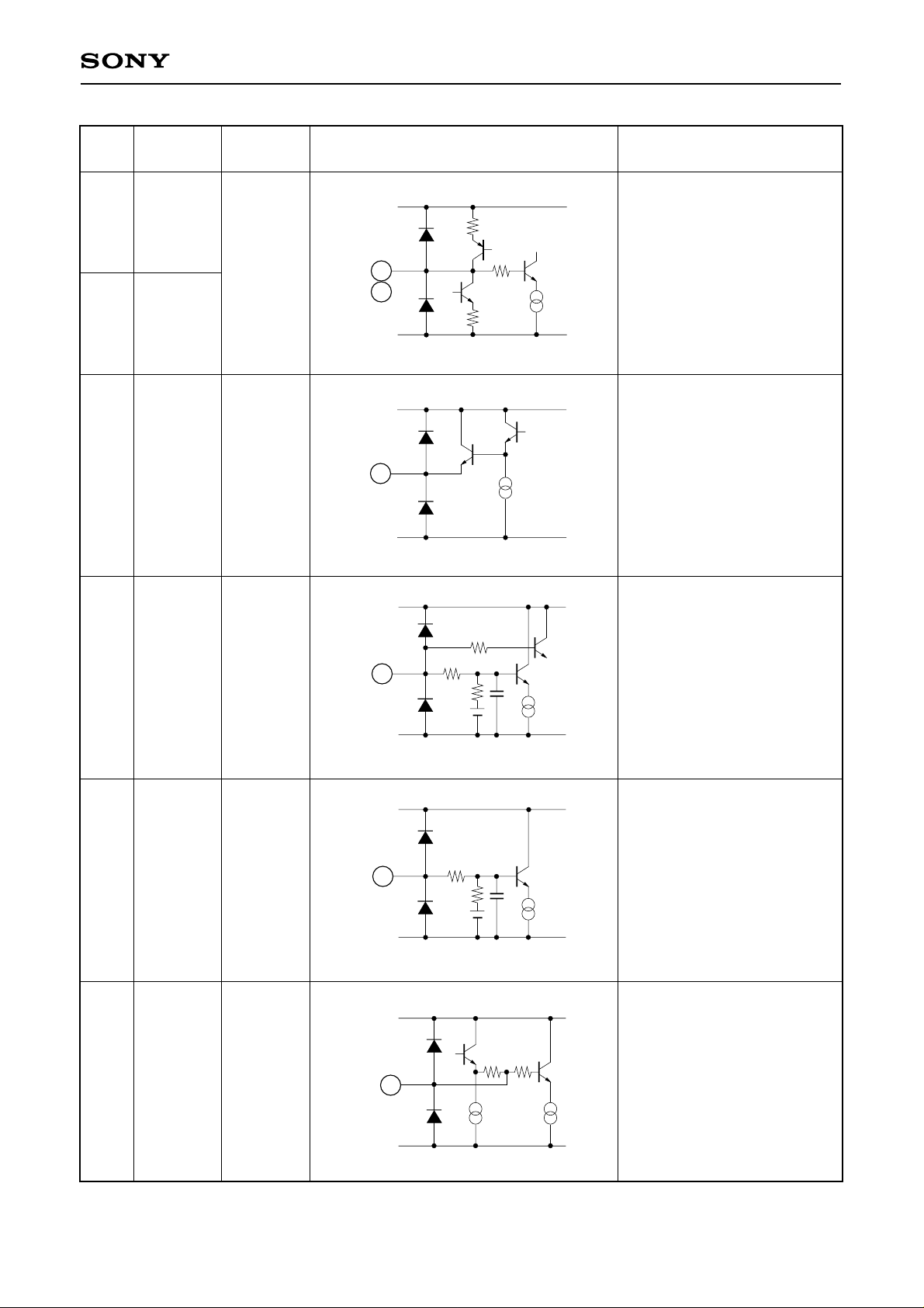
Analog Block Pin Description
CXA1854AR
Pin
No.
Symbol Pin voltage Equivalent circuit Description
1 SYNC IN
2 YIN 3.2V
CC1
V
1
GND1
V
GND1
CC1
2
200
50p
1k
Sync input.
Normally inputs the Y signal.
The standard signal input level
is 0.5Vp-p (up to 100% white
level from the sync chip).
Y signal input.
The standard signal input level
is 0.5Vp-p (up to 100% white
level from the sync chip).
Input at low impedance (75Ω or
less).
50µA
VCC1
3 AGCADJ VCC1/2 AGC gain adjustment pin.
4 AGCTC AGC detection filter connection.
5 PICT VCC1/2
3
GND1
VCC1
4
GND1
CC1
V
5
40k
50µA
20k
47k
2k
2.5V
1k
1k
Adjusts frequency
characteristics of luminance
signal.
Increasing the voltage
GND1
50µA
2.5V
emphasizes contours.
– 5 –
CXA1854AR
Pin
No.
Symbol Pin voltage Equivalent circuit Description
9 EXT-R
10 EXT-G
11 EXT-B
39 R OUT
41 G OUT
VCC2
2
VCC1
9
10
11
GND1
CC2
V
39
41
43
200
50
50
External digital signal input.
There are two threshold
values: Vth1 (approximately
1.2V) and Vth2 (approximately
2.2V). When one of the EXTRGB signals exceeds Vth1, all
of the RGB outputs go to
black level (black side clip
level); when an input exceeds
Vth2, only the corresponding
output goes to white level
(white side limiter level).
RGB primary color signal
output.
43 B OUT
40 FB R
42 FB G
44 FB B
46 BLKLIM
GND2
CC2
V
40
42
44
GND2
V
CC1
46
GND1
2k
2k
Smoothing capacitor
connection for the feedback
circuit of RGB output DC level
control.
Use a low-leakage capacitor
because of high impedance.
50k
Sets the RGB output amplitude
(black-black) clip level.
48 REG 4.2V
VCC1
48
GND1
60k
40k 40k
– 6 –
Smoothing capacitor
connection for the internally
generated constant voltage
source circuit.
Connect a capacitor of 1µF or
more.
CXA1854AR
Pin
No.
Symbol Pin voltage Equivalent circuit Description
49 B-YIN
50 R-YIN
51 COUT 2.3V
V
CC1
49
50
GND1
VCC1
51
GND1
2k
50µA
200
50µA
Color difference demodulation
circuit inputs during DPAL
mode.
Leave this pin open for NTSC.
Color difference signal is input
respectively when Y/color
difference input. (Standard
input is 0.15Vp-p.)
At this time, the bias is 3.5V.
Color adjusted chroma signal
is output.
When taking the chroma
signal, connect to GND with a
load resistor (approximately
5kΩ).
VCC1
6k
52
HUE/RST
3.2V
53 COLOR 3.2V Color adjustment.
54 XVXO 3.5V Crystal oscillator connection.
52
GND1
VCC1
53
GND1
VCC1
54
100k
12k
3.2V
100k
25k
3.2V
2k
5p
50µA
5p
50µA
500
Color phase adjustment pin
during NTSC.
Use for detective axis
adjustment of the R-Y/B-Y
axes during SPAL.
Also doubles as the reset pin.
The system is reset when this
pin is connected to GND.
GND1
– 7 –

CXA1854AR
Pin
No.
Symbol Pin voltage Equivalent circuit Description
55 RBRT
56 BBRT
57
RGB-GAIN
VCC1/2
VCC1/2
VCC1
55
56
GND1
VCC1
57
GND1
47k
47k
3k
3k
Fine adjustment for R and B
signal brightness.
2.5V
Adjusts RGB output amplitude
gain.
2.5V
58 GAMMA2 VCC1/2
59 GAMMA1 VCC1/2
60 BRIGHT VCC1/2
VCC1
58
GND1
VCC1
59
GND1
VCC1
60
GND1
47k
47k
47k
3k
3k
4k
Adjusts voltage gain change
point γ 2.
2.5V
Adjusts voltage gain change
point γ 1.
2.5V
RGB output brightness
adjustment. It does not
influence the γ compensation
curve.
2.5V
– 8 –
CXA1854AR
Pin
No.
61
CONTRAST
62 CIN
Symbol Pin voltage Equivalent circuit Description
VCC1
VCC1/2 Contrast adjustment.
61
GND1
VCC1
62
47k
4k
2.5V
20k
500
100µA 50µA
15p
Video signal input when using
composite input.
Chroma signal input when
using Y/C input.
Leave this pin open when
Y/color difference input.
GND1
63 R-GAIN
64 B-GAIN
VCC1/2
VCC1
63
64
GND1
47k
3k
Fine adjustment for R and B
signal contrast.
2.5V
– 9 –
CXA1854AR
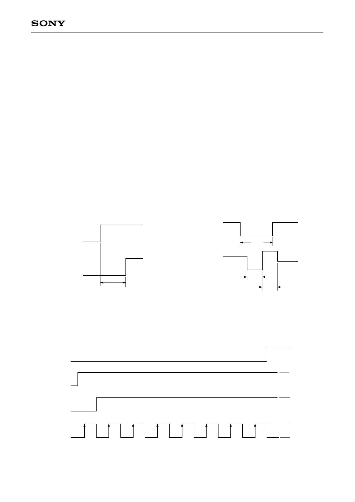
Setting Conditions for Measuring Electrical Characteristics
When measuring the DC characteristics, the TG block must be horizontally synchronized by performing Setting 2.
Setting 2 must also be performed when measuring the AC characteristics. When measuring items with bands
greater than 2MHz such as the Y frequency response or sharpness characteristics, settings 1 and 3 must also
be performed and measurements made with the sample-and-hold circuit set to through status.
Setting 1. System reset
After turning on the power, set SW52 to ON and start up V52 from GND in order to activate the
timing controller system reset. (See Fig. 1-1.)
Setting 2. Horizontal AFC adjustment
Input SIG6 (VL = 0mV) to (A) and adjust VR12 so that WL and WH of the TP12 output waveform are
the same. (See Fig. 1-2.)
Setting 3. S/H off
Input the signals shown in Fig. 1-3 to Pins 16, 17, 18 and 19 in order to set the sample-and-hold
circuit to through status.
VDD (VCC1)
V52 (RESET)
Fig. 1-1. System reset Fig. 1-2. Horizontal AFC adjustment
Pin 19
Pin 18
Pin 17
TR
R > 10µs
T
SIG6
TP12
WS
WL
WH
WL = WH
VDD
GND
V
DD
GND
DD
V
GND
Pin 16
VDD
GND
Fig. 1-3. S/H off input pattern
– 10 –
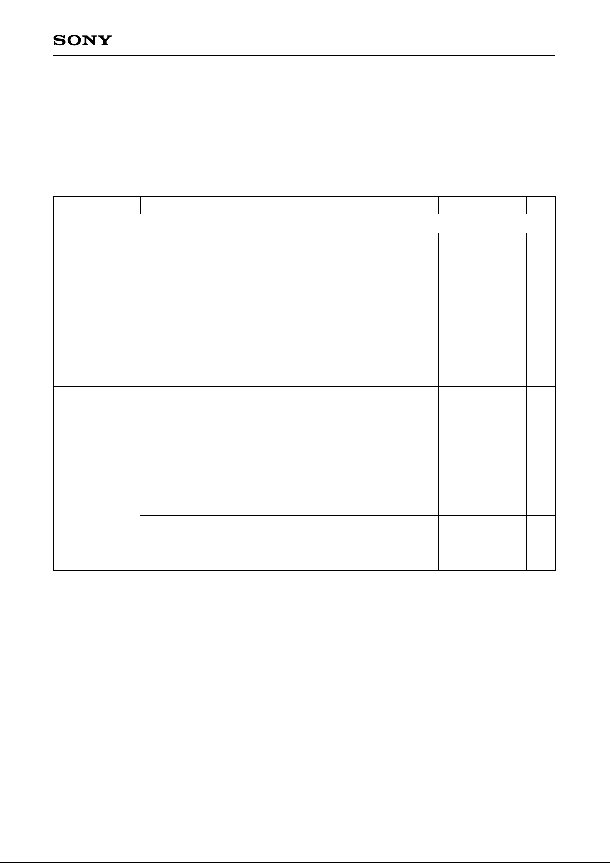
CXA1854AR
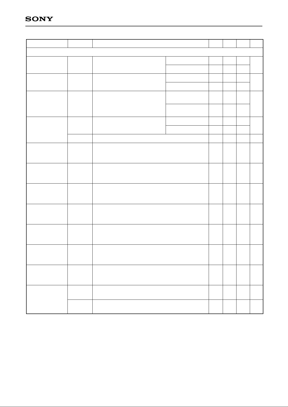
Electrical Characteristics – DC Characteristics (1)
Unless otherwise specified, Setting 2 and the following setting conditions are required.
VCC1 = 5.0V, VCC2 = 12.0V, GND1 = GND2 = GND, VDD = 5.0V, VSS = GND
V3, V5, V46, V55, V56, V57, V58, V59, V60, V61, V63, V64 = 2.5V
V52, V53 = 3.2V
SW3, SW5, SW46, SW52, SW53, SW55, SW56, SW57, SW58, SW59, SW60, SW61, SW63, SW64 = ON
Set SW7, SW8, SW9, SW10, SW11 and SW19 are setting A.
Item Symbol Conditions Min. Typ. Max. Unit
Power supply characteristics
Input SIG5 to (A) and SIG3 (0dB) to (B).
Current
consumption V
CC1
ICC11
I
CC12
ICC13
Measure the I
Input SIG5 to (A) and SIG3 (0dB) to (B).
Set SW8 to C.
Measure the I
Input SIG5 to (A) and SIG5 to (F) and (G).
Set SW8 to B.
Measure the I
CC1 current value.
CC1 current value.
CC1 current value.
Y/color difference input mode
COMP input mode
Y/C input mode
35
34
32
44
42.5
40
53
51
48
mA
mA
mA
Current
consumption V
Current
consumption V
CC2
DD
CC2
I
IDD1
I
DD2
IDD3
Input SIG5 to (A) and SIG3 (0dB) to (B).
Measure the I
CC2 current value.
Input SIG5 to (A) and SIG3 (0dB) to (B).
Measure the I
DD current value.
Input SIG5 to (A) and SIG3 (0dB) to (B).
Set SW19 to B.
Measure the I
DD current value.
Input SIG5 to (A) and SIG3 (0dB) to (B).
Set SW19 to B.
Measure the I
DD current value.
LCX009 mode
LCX005 mode
V
DD = 3.0V
LCX005 mode
3
5.5
7
10.5
5
2
8
mA
14
mA
8
10.5
3
4.5
mA
mA
– 11 –
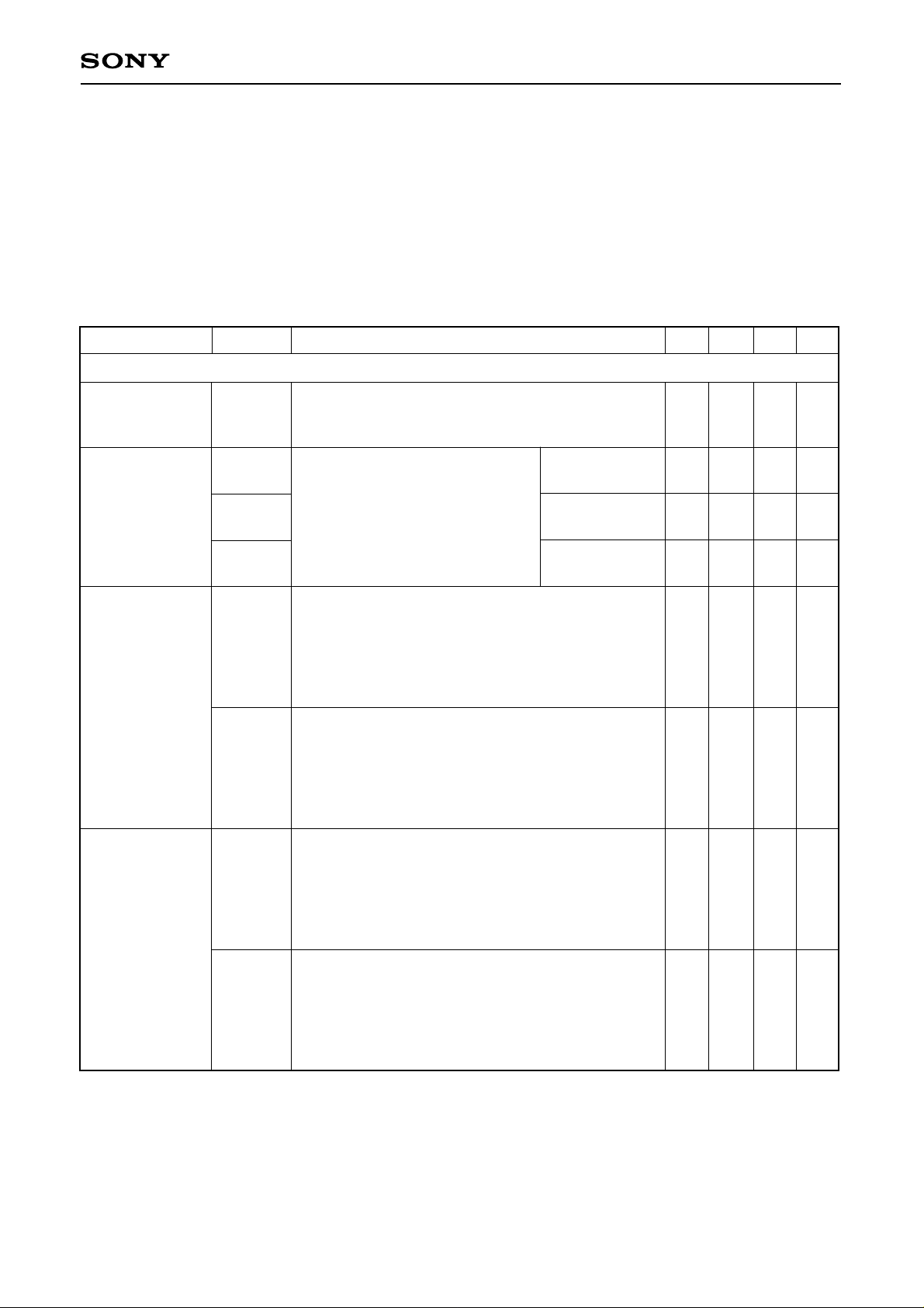
Item Symbol Conditions Min. Typ. Max. Unit
Digital block I/O characteristics
∗
Input current 1
Input current 2
II1
II2
Input pin with pull-up resistor
VIN = VSS
Input pin with pull-down resistor
VIN = VDD
1
∗
2
VDD = 5.0V
VDD = 3.0V
VDD = 5.0V
VDD = 3.0V
–240
–144
40
24
–100
–60
100
60
CXA1854AR
–40
µA
–24
240
µA
144
High level output
voltage
Output pins except
CKO and RPD
Low level output
voltage
Output pins except
CKO and RPD
High level output
voltage
CKO pin
Low level output
voltage
CKO pin
High level output
voltage
RPD pin
Low level output
voltage
RPD pin
Output off leak
current
RPD pin
VOH1
VOL11
VOL12
VOH2
VOL2
VOH3
VOL3
IOFF
∗
IOH = –2mA
IOL = 2mA
IOL = 500µA
3
∗
3
∗
3
IOH = –3mA
IOL = 3mA
IOH = –1mA
IOL = 1.5mA
High impedance status
VOUT = V
SS or VOUT = VDD
DD = 5.0V
V
VDD = 3.0V
V
DD = 5.0V
VDD = 3.0V
VDD
–
V
–
0.5V
VDD
–1.2
–40
0.8
DD
1.0
DD
0.5
0.6
0.3
0.5VDD
1.0
40
V
V
V
V
V
V
V
µA
High level input
voltage
VIH
CMOS input cell
0.7VDD
SLCK and RGT pins
Low level input
voltage
VIL
CMOS input cell
0.3V
SLCK and RGT pins
Ternary input
switching
MDTHL
threshold voltage
(MODE1/MODE2)
∗1
Input pins with pull-up resistors: RGT, TEST6, TEST7, TEST8
∗2
Input pins with pull-down resistors: SLCK, TEST0, TEST1, TEST2, TEST5
∗3
Output pins except CKO and RPD: HD, VD, VST1, VCK1, VCK2, CLR, EN, HST1, HCK1, HCK2, TEST3,
MDTHH
MODE M → L level threshold
SW7, SW8 = B
MODE M → H level threshold
SW7, SW8 = B
0.2VDD
0.6VDD
0.3VDD
0.7VDD
0.4VDD
0.8VDD
TEST4
– 12 –
DD
V
V
V
V
CXA1854AR
Electrical Characteristics – AC Characteristics (1)
Unless otherwise specified, Setting 2 and the following setting conditions are required.
Vcc1 = 5.0V, Vcc2 = 12.0V, GND1 = GND2 = GND, (VDD = 5.0V, VSS = GND)
V5, V55, V56, V57, V60, V61, V63, V64 = 2.5V V3, V58 = 0V V46, V59 = 5.0V
V52, V53 = 3.2V
SW3, SW5, SW46, SW52, SW53, SW55, SW56, SW57, SW58, SW59, SW60, SW61, SW63, SW64 = ON
Set SW7, SW8, SW9, SW10, SW11 and SW19 are setting A.
Unless otherwise specified, measure the non-reversed outputs for TP39, TP41 and TP43.
Item Symbol Conditions Min. Typ. Max. Unit
Y signal block
Video maximum
gain
Y signal frequency
Characteristics
Sharpness
characteristics
MAX
Sharpness
characteristics
MIN
GV
FCYYC
FCYCMN
FCYCMP
GSHPMXC
GSHPMXY
GSHPMNC
GSHPMNY
Input SIG5 to (A) and measure the ratio between the
output amplitude (white-black) and input amplitude at
TP41.
Assume the output amplitude at
TP41 when SIG2 (0dB, no burst,
100kHz) is input to (A) as 0dB. Vary
the frequency of the input signal to
obtain the frequency with an output
amplitude of –3dB. Settings 1 and 3
are required.
Assume the output amplitude at TP41 when SIG8
(100kHz) is input to (A) as 0dB. Obtain the output
amplitude ratio for the input SIG8 (2.0MHz).
V5 = 4.0V
Settings 1 and 3 are required.
Assume the output amplitude at TP41 when SIG8
(100kHz) is input to (A) as 0dB. Obtain the output
amplitude ratio for the input SIG8 (2.5MHz).
V5 = 4.0V, SW8 = C
Settings 1 and 3 are required.
Assume the output amplitude at TP41 when SIG8
(100kHz) is input to (A) as 0dB. Obtain the output
amplitude ratio for the input SIG8 (2.0MHz).
V5 = 0V
Settings 1 and 3 are required.
Assume the output amplitude at TP41 when SIG8
(100kHz) is input to (A) as 0dB. Obtain the output
amplitude ratio for the input SIG8 (2.5MHz).
V5 = 0V, SW8 = C
Settings 1 and 3 are required.
Y/C input,
SW8 = C
Composite input
(NTSC)
Composite input
(PAL), SW7 = C
Composite input
Y/C input
Composite input
Y/C input
13.5
5.0
2.5
3.0
7
10
16.5
12
16
–1
1
19.5
2
4
dB
MHz
MHz
MHz
dB
dB
dB
dB
– 13 –
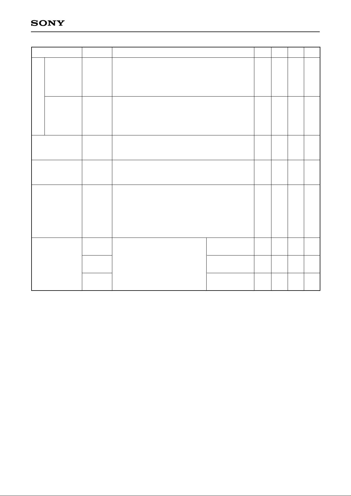
Item Symbol Conditions Min. Typ. Max. Unit
Adjust the output amplitude at TP41 when SIG1 (APL:
50%) is input to (A) to 1.5Vp-p with V61. Assume this as
APL = 90%
APL = 10%
AGC characteristics
GAPL90
GAPL10
0 dB, and obtain the TP41 output amplitude ratio when
input SIG1 (APL: 90%) is input.
V3 = 2.5V, V60 = 3.5V
Adjust the output amplitude at TP41 when SIG1 (APL:
50%) is input to (A) to 1.5Vp-p with V61. Assume this as
0dB, and obtain the TP41 output amplitude ratio when
input SIG1 (APL: 10%) is input.
V3 = 2.5V, V60 = 3.5V
–4
–2.5
1
2.5
CXA1854AR
dB
–1
dB
4
Contrast
characteristics
MAX
Contrast
characteristics MIN
Carrier leak
(residual carrier)
Y signal I/O delay
time
GCNTMX
GCNTMN
CRRLK
TDYYC
TDYCMN
TDYCMP
Input SIG5 to (A) and obtain the ratio between the TP41
output amplitude when V61 = 2.5V and the TP41 output
amplitude when V61 = 5V.
Input SIG5 to (A) and obtain the ratio between the TP41
output amplitude when V61 = 2.5V and the TP41 output
amplitude when V61 = 1V.
Input SIG3 (0dB) to (A) and (B). Adjust the chroma signal
phase so that the amplitude (black – white) at TP43 is at a
maximum. Using a spectrum analyzer, measure the input
and the 3.58MHz or 4.43MHz component, and obtain
CRRLK = 150mV × 10
∆d/20
using their difference ∆d.
SW7 = A for NTSC measurement, and C for PAL
measurement.
Input SIG6 (VL = 150mV) to (A).
Measure the delay time from the
rising edge of the input signal to the
rising edge of the non-reversed
output.
V5 = 2V
Y/C input
SW8 = C
Composite input
(NTSC)
Composite input
(PAL), SW7 = C
2
250
630
610
5
–10
400
780
760
–6
30
550
930
910
dB
dB
mVpp
ns
ns
ns
– 14 –
 Loading...