

Sony CXA1853AQ Datasheet

RGB Driver for LCD
Description
The CXA1853AQ is an RGB driver for LCD panels.
It supports a line alternative RGB drive system.
Features
• Built-in RGB signal phase matching sample-and-
hold circuit
• Effective frequency response (18MHz Typ.)
• Built-in gain and breakpoint variable 2-point γ
compensation circuit
• Built-in side black generation circuit for 4:3/16:9
aspect conversion
• Built-in VCOM voltage output circuit
Structure
Bipolar silicon monolithic IC
Applications
• Liquid crystal projectors
• Liquid crystal viewfinders
• Compact liquid crystal monitors
CXA1853AQ
80 pin QFP (Plastic)
Absolute Maximum Ratings (Ta = 25°C)
• Supply voltage VCC16 V
VCC215 V
•Input pin voltage VIN VCC1V
•Operating temperature Topr –25 to +75 °C
• Storage temperature Tstg –55 to +150 °C
• Allowable power dissipation
PD 1500 mW
Operating Conditions
• Supply voltage VCC1 4.75 to 5.25 V
VCC2 11.0 to 14.0 V
• RGB input signal voltage
VIN 0.7 Vp-p
Note)
Note) Defined as the amplitude from the pedestal
level to white.
Sony reserves the right to change products and specifications without prior notice. This information does not convey any license by
any implication or otherwise under any patents or other right. Application circuits shown, if any, are typical examples illustrating the
operation of the devices. Sony cannot assume responsibility for any problems arising out of the use of these circuits.
– 1 –
E96334-PS
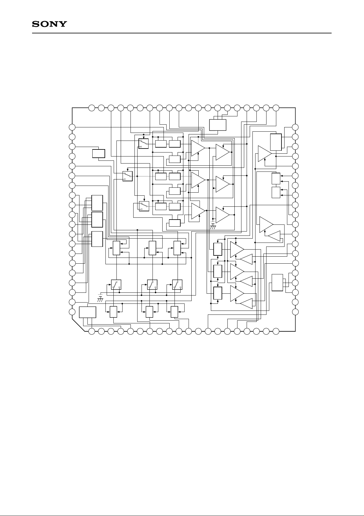
Block Diagram
CXA1853AQ
4
N.C.
SH2
SH3
SH4
N.C.
60
59
57
58
GND
55
56
SIG SEL
54
GCA DETR
53
52
GCA DETG
GCA DETB
50
51
CC
V
IREF
49
48
GND
B GAIN
47
R GAIN
46
RGB GAIN
45
44
XCLP1
43
XCLP2
WHT LIM
GAM SEL
4142
SH1
PV
SH IN
GND
B CLAMP
G CLAMP
R CLAMP
RGB GAM GAIN1
R GAM GAIN1
B GAM GAIN1
RGB GAM GAIN2
R GAM GAIN2
B GAM GAIN2
RGB GAM CTR2
R GAM CTR2
B GAM CTR2
RGB GAM CTR1
R GAM CTR1
B GAM CTR1
N.C.
61
62
CC
S/H
γ AMP
S/HS/H
S/H
S/HS/H
S/H
S/H
S/H
GCA
GCA
GCA
γ AMP
CLP
63
BRT
CONT
CLP
R γ
RGB γ
B γ
CONT
CONT
CONT
CLP
γ AMP
CLP
64
65
66
67
68
69
70
71
72
73
74
75
76
77
78
79
80
GAIN
CONT
EA
EA
EA
SW
SW
SW
BUFFSW
BUFF
BUFF
BUFF
BUFF
BUFF
CTRL
BLKLMT
PRG
SID
SBRT
CONT
40
BLK CENT
39
BLK LIM
38
VCOM OUT
37
SIG CENT CTR
36
VCOM CTR
35
PRG
34
GND
33
SID FRP
32
FRP
31
PRG CTR
30
SID CTR
29
SID CLP
28
R CLP
27
G CLP
26
B CLP
25
R SBRT
B SBRT
24
23
RGB SBRT
GND
22
N.C.
21
1
2
N.C.
RGB MBRT
3
N.C.
4
R MBRT
5
B MBRT
6
N.C.
8
7
GAM OUT
BIN
12
GND
13
SID OUT
14 15
2
CC
V
16
R OUT
17
G OUT
9
10
RIN
11
GIN
1
CC
V
18
B OUT
19
20
3
CC
N.C.
V
N.C.
– 2 –
CXA1853AQ
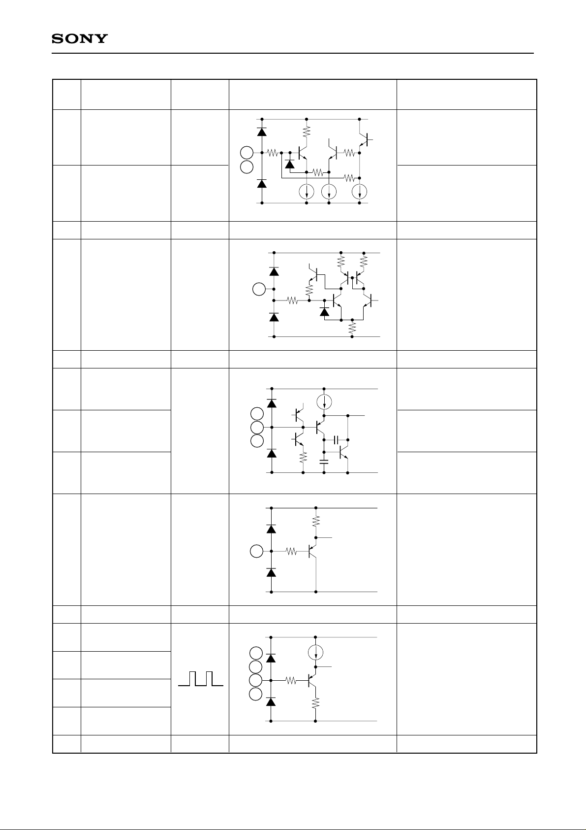
Pin Description (VCC1 = 5V, VCC2 = 13V)
Pin
NO.
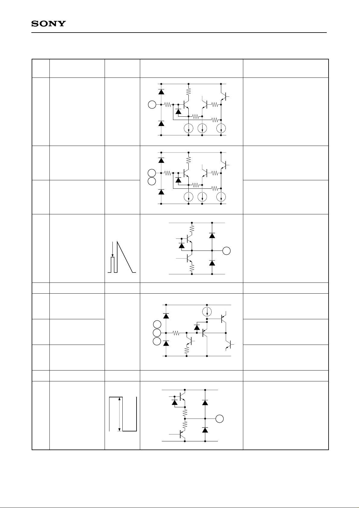
Symbol Pin voltage Equivalent circuit Description
1 RGB MBRT
4 R MBRT
5 B MBRT
7 GAM OUT
1.6 to 5.0V
1.6 to 5.0V
1.6 to 5.0V
2V
Reference level
VCC1
2k
40µA
80k
80k
80k
80k
RGB signal common main
brightness control. Preset
internally to 3.3V.
40µA
R signal main brightness
control. Preset internally to
3.3V.
200
1
∗
40µA
GND
VCC1
∗
200
4
5
37k
5k
74k
B signal main brightness
∗
GND
20µA
20µA
VCC1
100
40µA
control. Preset internally to
3.3V.
G signal output of which main
bright and gamma are
7
adjusted and insert the
reference signal.
GND
100
8VCC1 5V 5V power supply.
9 RIN
10 GIN
11 BIN
12 GND GND.
SID OUT SID signal output.
13
0V
9.3Vp-p
Typ.
VCC1
10
11
GND
VCC2
GND
50µA
9
200
6.2k
10
10
13
R signal input.
Input a 0.7Vp-p signal.
G signal input.
Input a 0.7Vp-p signal.
B signal input.
Input a 0.7Vp-p signal.
Note 1)∗ in the Pin voltage indicates external applied voltage.
Note 2) Defined as the amplitude from the pedestal level to white.
Note 2)
Note 2)
Note 2)
– 3 –

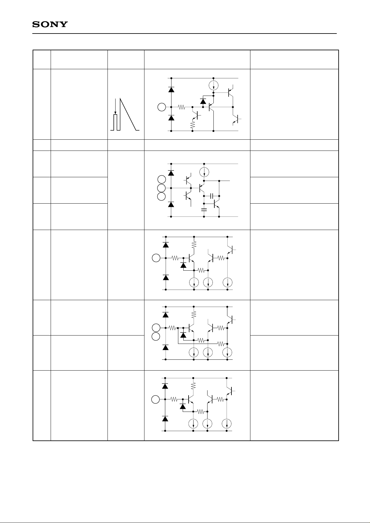
CXA1853AQ
Pin
NO.
14 VCC2 13V
15 R OUT R signal output.
16 G OUT G signal output.
17 B OUT B signal output.
18 VCC3 5V power supply.
22 GND GND.
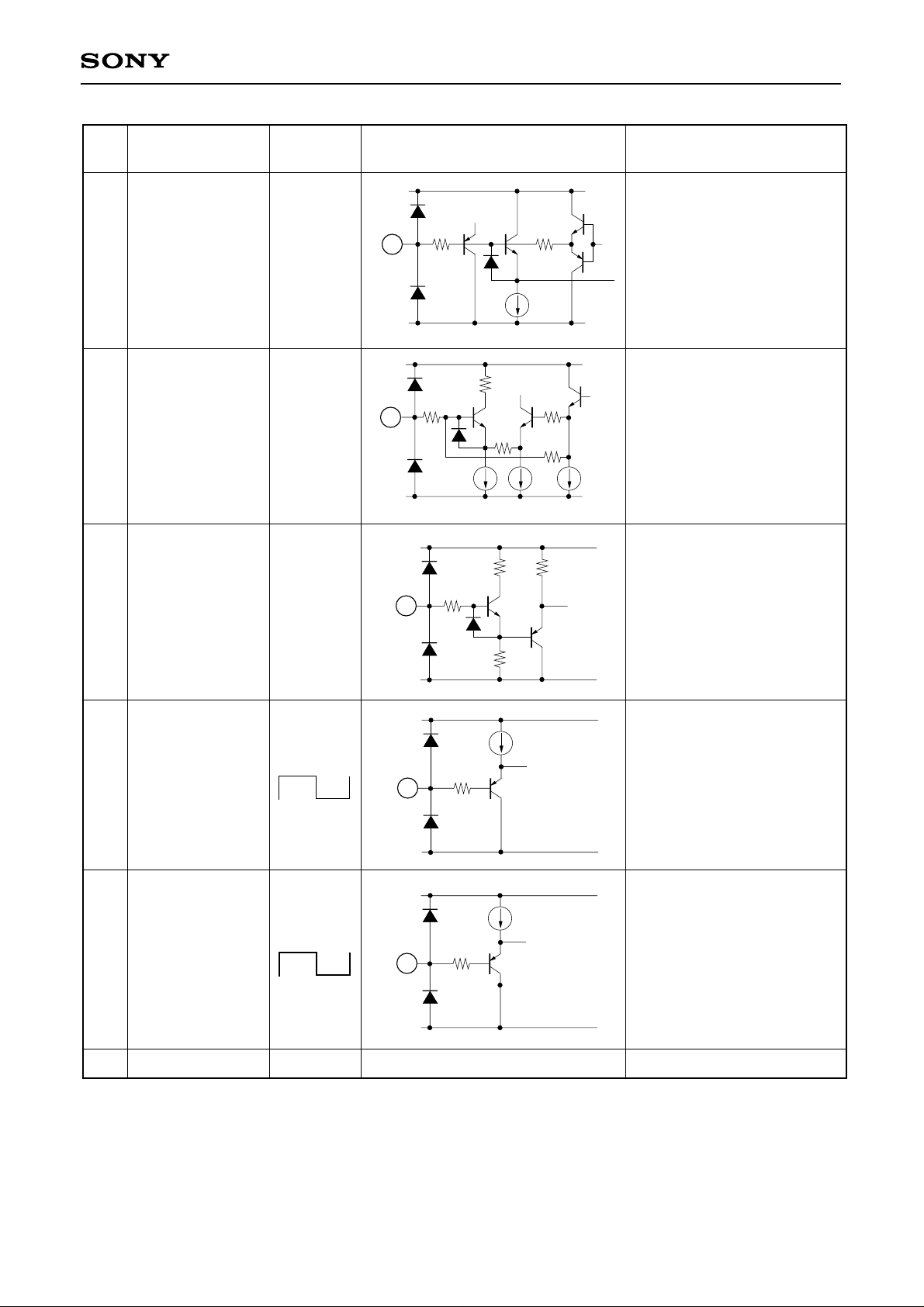
23 RGB SBRT
Symbol Pin voltage Equivalent circuit Description
13V power supply.
VCC2
4.5V
Typ.
10
10
GND
15
16
17
5V
0V
VCC3
3k
1.6 to 5.0V
200
23
∗
53µA 13µA
GND
27k
200
RGB signal common sub
brightness control.
53µA
VCC3
24 B SBRT
25 R SBRT
26 B CLP
27 G CLP
28 R CLP
1.6 to 5.0V
1.6 to 5.0V
4.7 to 8.3V
∗
24
25
∗
GND
VCC2
26
∗
27
28
GND
3k
200
26µA 40µA
200
Note)∗in the Pin voltage indicates external applied voltage.
118k
26µA
80k
80k
2k
10µA
B signal sub brightness
control.
Preset internally to 3.3V.
R signal sub brightness
control.
Preset internally to 3.3V.
B output detection signal
input.
G output detection signal
input.
R output detection signal
input.
– 4 –
CXA1853AQ
Pin
NO.
Symbol Pin voltage Equivalent circuit Description
29 SID CLP
30 SID CTR
31 PRG CTR
4.7 to 8.3V
1.6 to 5.0V
1.6 to 5.0V
VCC2
SID output detection signal
200
29
∗
2k
input.
Use an average value
detecting external capacitor
with a small leak current
10µA
GND
VCC3
3k
200
30
∗
53µA 40µA
GND
VCC3
200
∗
31
35k
3k
80k
80k
53µA
90k
absolute value and
tolerance.
SID output amplitude control.
Preset internally to 3.3V.
Level control for the PRG
signal inserted into the SID
signal.
90k
GND
VCC3
10µA
32 FRP
33
SID FRP
34 GND GND.
0V
0V
5V
32
GND
VCC3
5V
33
GND
0V
200
10µA
200
Note)∗in the Pin voltage indicates external applied voltage.
FRP input. This pulse is
used to invert the polarity of
the RGB output. Output is
inverted when Low, and noninverted when High.
Input level: High ≥ 4V
Low ≤ 1V
FRP pulse input for SID
output. This pulse is used to
invert the polarity of the SID
output. Output is inverted
when Low, and non-inverted
when High.
Input level: High ≥ 4V
Low ≤ 1V
– 5 –

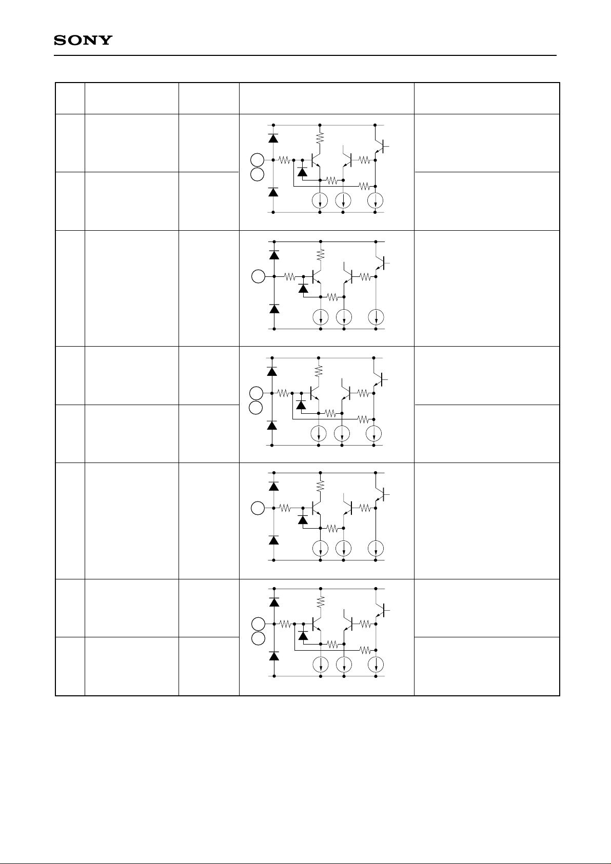
CXA1853AQ
Pin
NO.
Symbol Pin voltage Equivalent circuit Description
35 PRG
36 VCOM CTR
37 SIG CENT CTR
5V
0V
1.6 to 5.0V
1.6 to 5.0V
VCC3
10µA
PRG pulse input.
This pulse is used to insert
35
200
the PRG signal into the SID
output.
Input level: High ≥ 4V
Low ≤ 1V
GND
VCC2
200
36
∗
17µA
GND
VCC2
200
37
∗
50k
50k
80k
80k
40µA
17µA
80k
80k
VCOM voltage control. The
VCOM voltage variable
range is –0.8V to +1.3V with
respect to the signal center
voltage.
RGB and SID signal center
voltage control.
26µA 40µA
GND
VCC2
38 VCOM OUT VCOM voltage output.
39 BLK LIM
3.4 to 9.1V
1.6 to 5.0V
∗
GND
VCC2
200
39
∗
2k
10
10
127k
26µA
100k
100k
38
Limiter control for limiting the
output amplitude of the RGB
signal. Preset internally to
3.3V.
20µA 40µA
GND
20µA
Note)∗in the Pin voltage indicates external applied voltage.
– 6 –
CXA1853AQ
Pin
NO.
Symbol Pin voltage Equivalent circuit Description
40 BLK CENT
41 WHT LIM
42 GAM SEL
1.6 to 5.0V
1.6 to 5.0V
∗
5.0V
VCC2
2k
200
40
∗
50k
100k
100k
RGB signal output limiter
center control. Preset
internally to 3.3V.
When preset, the limiter
center becomes equal to the
20µA 40µA
GND
VCC3
200
41
∗
20µA 40µA
GND
VCC1
200
42
2k
55k
37k
20µA
100k
100k
20µA
RGB output center.
RGB signal white peak
limiter control. Preset
internally to 3.3V.
Gamma circuit control.
Gamma ON when High,
gamma OFF when Low.
Input level: High ≥ 4V
Low ≤ 1V
GND
5V
43 XCLP2
44 XCLP1
45
RGB GAIN
0V
2.0µs
5V
0V
1.2µs
1.6 to 5.0V
VCC1
55k
200
43
44
GND
VCC4
1.5k
200
45
∗
40µA 20µA
GND
Note)∗in the Pin voltage indicates external applied voltage.
38k
40µA
200
Reference signal pulse input.
Reference level when Low.
Input level: High ≥ 4V
Low ≤ 1V
Clamp pulse input. Clamped
when Low.
Input level: High ≥ 4V
Low ≤ 1V
Gain control for RGB signal
common variable gain
amplifier.
– 7 –
CXA1853AQ
Pin
NO.
46 R GAIN
Symbol Pin voltage Equivalent circuit Description
1.6 to 5.0V
VCC4
200
1k
48k
80k
80k
∗
46
47
Gain control for R signal
variable gain amplifier.
Preset internally to 3.3V.
Gain control for B signal
47 B GAIN
1.6 to 5.0V
48 GND GND.
49 IREF
50 VCC4 5V power supply.
1.2V
5.0V
∗
GND
0V
VCC4
80µA 40µA
80µA
49
GND
2k
200
variable gain amplifier.
Preset internally to 3.3V.
5k 5k
Sample-and -hold circuit
current setting.
10k
51 GCADET B
52 GCADET G
53 GCADET R
54 SIG SEL
55 GND
56 SH4
57 SH3
58 SH2
61 SH1
1.8V Typ.
0 to 5.0V
0V
5V
0V
VCC4
40µA
51
52
53
6.2k
GND
VCC4
55k
∗
54
200
B GCA circuit clamp
detection.
G GCA circuit clamp
detection.
R GCA circuit clamp
detection.
Selection of input signal to
Sample-and -hold circuit.
R and B signals selected
when High, G signal selected
when Low.
Input level: High ≥ 4V
GND
Low ≤ 1V
GND.
PVCC
56
57
58
59
GND
100µA
200
100
Sample-and-hold pulse
input.
Input level: High ≥ 3.0V
Low ≤ 1.0V
Sampling when High, hold
when Low.
62 PVCC
5V
Note)∗in the Pin voltage indicates external applied voltage.
– 8 –
5V power supply.
CXA1853AQ
Pin
NO.
63 SH IN
64 GND GND.
65 B CLAMP B signal clamp detection.
66 G CLAMP G signal clamp detection.
67 R CLAMP R signal clamp detection.
Symbol Pin voltage Equivalent circuit Description
2.25V
Reference level
VCC4
63
GND
200
6.2k
100µA
Sample-and-hold circuit
input.
0V
VCC1
40µA
65
2.1V Typ.
66
67
GND
68
69
70
71
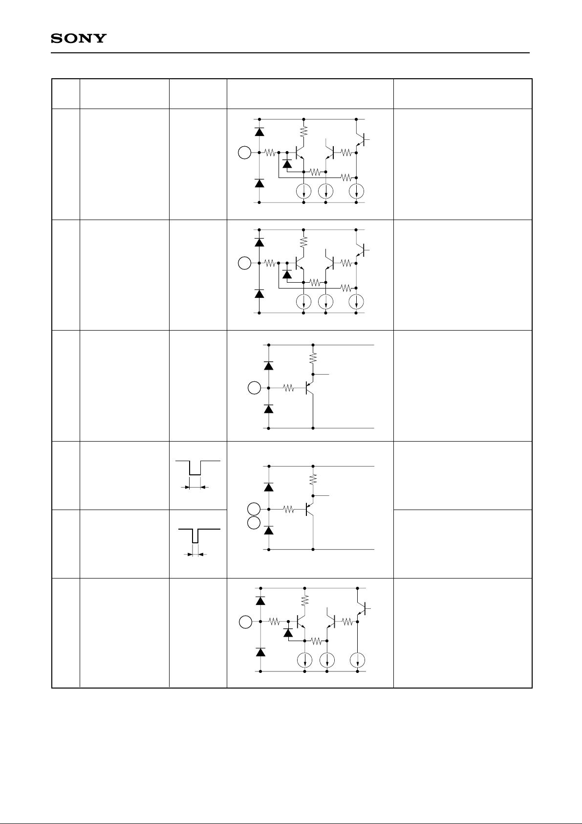
RGB GAM
GAIN 1
R GAM
GAIN 1
B GAM
GAIN 1
RGB GAM
GAIN 2
1.6 to 5.0V
1.6 to 5.0V
1.6 to 5.0V
1.6 to 5.0V
VCC1
1k
200
68
∗
40µA
GND
VCC1
∗
200
69
70
37k
1k
37k
40µA
200
80k
80k
RGB signal common black
side voltage gain control.
40µA
R signal black side voltage
gain control. Preset internally
to 3.3V.
B signal black side voltage
∗
GND
VCC1
71
∗
40µA 40µA
40µA
1k
200
37k
200
gain control. Preset internally
to 3.3V.
RGB signal common white
side voltage gain control.
40µA
GND
Note)∗in the Pin voltage indicates external applied voltage.
– 9 –
40µA
40µA
CXA1853AQ
Pin
NO.
72
73
74
75
76
Symbol Pin voltage Equivalent circuit Description
R GAM
GAIN 2
B GAM
GAIN 2
RGB GAM
CTR 2
R GAM
CTR 2
B GAM
CTR 2
1.6 to 5.0V
1.6 to 5.0V
1.6 to 5.0V
1.6 to 5.0V
1.6 to 5.0V
VCC1
∗
72
73
∗
GND
VCC1
74
∗
GND
VCC1
∗
75
76
∗
GND
1k
200
37k
40µA 40µA
1k
200
37k
40µA 40µA
3k
200
74k
20µA 40µA
80k
80k
40µA
200
40µA
80k
80k
20µA
R signal white side voltage
gain control. Preset internally
to 3.3V.
B signal white side voltage
gain control. Preset internally
to 3.3V.
RGB signal common white
side voltage gain change
point control.
R signal white side voltage
gain change point control.
Preset internally to 3.3V.
B signal white side voltage
gain change point control.
Preset internally to 3.3V.
VCC1
1k
200
77
∗
40µA 40µA
GND
VCC1
∗
78
79
∗
GND
3k
200
20µA 40µA
77
78
79
RGB GAM
CTR 1
R GAM
CTR 1
B GAM
CTR 1
1.6 to 5.0V
1.6 to 5.0V
1.6 to 5.0V
Note)∗in the Pin voltage indicates external applied voltage.
37k
74k
40µA
20µA
200
80k
80k
RGB signal common black
side voltage gain change
point control.
R signal black side voltage
gain change point control.
Preset internally to 3.3V.
B signal black side voltage
gain change point control.
Preset internally to 3.3V.
– 10 –
Electrical Characteristics
Unless otherwise specified: Ta = 25°C, VCC1 = VCC3 = VCC4 = PVCC = 5V, VCC2 = 13V
SW1 = OFF, SW4 = OFF, SW5 = OFF, SW9 = a, SW10 = a, SW11 = a,
SW24 = OFF, SW25 = OFF, SW26 = a, SW27 = a, SW28 = a, SW29 = a,
SW30 = OFF, SW36 = OFF, SW37 = OFF, SW39 = OFF, SW40 = OFF,
SW41 = OFF, SW46 = OFF, SW47 = OFF, SW51 = a, SW52 = a,
SW53 = a, SW63 = a, SW65 = a, SW66 = a, SW67 = a, SW69 = OFF,
SW70 = OFF, SW72 = OFF, SW73 = OFF, SW75 = OFF, SW76 = OFF,
SW78 = OFF, SW79 = OFF, V23 = 3.1V, V31 = 3.5V, V42 = 5.0V,
V45 = 2.8V, V54 = 5.0V, V68 = 1.6V, V71 = 1.6V, V74 = 1.6V, V77 = 5.0V
Set (R IN), (G IN), (B IN) and (TEST IN) = 0V, (SH1), (SH2), (SH3) and
(SH4) = 5V, and input SG4 to (FRP) and (SID FRP), SG5 to (PRG),
SG2 to (XCLP2) and SG3 to (XCLP1).
CXA1853AQ
No. Item Symbol Measurement conditions Unit
1
Current consumption (1)
2
Current consumption (2)
3
Current consumption (3)
4
Current consumption (4)
5
Current consumption (5)
6
R IN pin current “Z”
7
R IN pin current “H”
8
R IN pin current “L”
9
G IN pin current “Z”
10
G IN pin current “H”
11
G IN pin current “L”
12
B IN pin current “Z”
13
B IN pin current “H”
14
B IN pin current “L”
15
RGB SBRT pin current
16
B CLP pin current
I
CC1
ICC2
ICC3
ICC4
ICC5
IZ9
IH9
IL9
IZ10
IH10
IL10
IZ11
IH11
IL11
I23
I26
Measure the current entering Pin 8.
Measure the current entering Pin 14.
Measure the current entering Pin 18.
Measure the current entering Pin 50.
Measure the current entering Pin 62.
SW9 → b, (XCLP1) = 5V, V9 = 2.4V
SW9 → b, (XCLP1) = 0V, V9 = 3.4V
SW9 → b, (XCLP1) = 0V, V9 = 1.4V
SW10 → b, (XCLP1) = 5V, V10 = 2.4V
SW10 → b, (XCLP1) = 0V, V10 = 3.4V
SW10 → b, (XCLP1) = 0V, V10 = 1.4V
SW11 → b, (XCLP1) = 5V, V11 = 2.4V
SW11 → b, (XCLP1) = 0V, V11 = 3.4V
SW11 → b, (XCLP1) = 0V, V11 = 1.4V
V23 = 5.0V
SW26 → b, V26 = 7.0V
Min. Typ. Max.
—
30
44
—
11
18
—
6
10
—
29
43
—
4
7
–1.5
–1.5
–1.5
–0.2
13
—
13
—
13
—
—
0
25
–25
0
25
–25
0
25
–25
2.5
0
1.5
—
–13
1.5
—
–13
1.5
—
–13
6
0.2
mA
mA
mA
mA
mA
µA
µA
µA
µA
µA
µA
µA
µA
µA
µA
µA
17
G CLP pin current
18
R CLP pin current
19
SID CLP pin current
20
PRG CTR pin current
21
FRP pin current “H”
22
FRP pin current “L”
23
SID FRP pin current “H”
24
SID FRP pin current “L”
25
PRG pin current “H”
26
PRG pin current “L”
27
GAM SEL pin current “H”
I27
I28
I29
I31
IH32
IL32
IH33
IL33
IH35
IL35
IH42
SW27 → b, V27 = 7.0V
SW28 → b, V28 = 7.0V
SW29 → b, V29 = 7.0V
V31 = 5.0V
(FRP) = 5V
(FRP) = 0V
(SID FRP) = 5V
(SID FRP) = 0V
(PRG) = 5V
(PRG) = 0V
V42 = 5V
– 11 –
–0.2
–0.2
–0.2
—
–0.1
–0.3
–0.1
–0.3
–0.1
–0.3
–0.1
0
0
0
0.3
0
–0.1
0
–0.1
0
–0.1
0
0.2
0.2
0.2
0.8
0.1
—
0.1
—
0.1
—
0.1
µA
µA
µA
µA
µA
µA
µA
µA
µA
µA
µA
CXA1853AQ
No. Item Symbol Measurement conditions Min. Typ. Max. Unit
28
GAM SEL pin current “L”
29
XCLP2 pin current “H”
30
XCLP2 pin current “L”
31
XCLP1 pin current “H”
32
XCLP1 pin current “L”
33
RGB GAIN pin current
34
GCA DET B pin current “Z”
35
GCA DET B pin current “H”
36
GCA DET B pin current “L”
37
GCA DET G pin current “Z”
38
GCA DET G pin current “H”
39
GCA DET G pin current “L”
40
GCA DET R pin current “Z”
IL42
IH43
IL43
IH44
IL44
I45
IZ51
IH51
IL51
IZ52
IH52
IL52
IZ53
V42 = 0V
(XCLP2) = 5V
(XCLP2) = 0V
(XCLP1) = 5V
(XCLP1) = 0V
V45 = 5V
SW51 → b, (XCLP1) = 5V, V51 = 2.0V
SW51 → b, (XCLP1) = 0V, V51 = 3.0V
SW51 → b, (XCLP1) = 0V, V51 = 1.0V
SW52 → b, (XCLP1) = 5V, V52 = 2.0V
SW52 → b, (XCLP1) = 5V, V52 = 3.0V
SW52 → b, (XCLP1) = 5V, V52 = 1.0V
SW53 → b, (XCLP1) = 5V, V53 = 2.0V
—
–0.1
—
–0.1
–1.0
—
–0.5
15
—
–0.5
15
—
–0.5
–1.7
0
–1.0
0
–0.2
0.5
0
30
30
0
30
–30
0
–0.4
0.1
–0.3
0.1
—
1.3
0.5
—
–15
0.5
—
–15
0.5
µA
µA
µA
µA
µA
µA
µA
µA
µA
µA
µA
µA
µA
41
GCA DET R pin current “H”
42
GCA DET R pin current “L”
43
SIG SEL pin current “H”
44
SIG SEL pin current “L”
45
SH4 pin current “H”
46
SH4 pin current “L”
47
SH3 pin current “H”
48
SH3 pin current “L”
49
SH2 pin current “H”
50
SH2 pin current “L”
51
SH1 pin current “H”
52
SH1 pin current “L”
53
SH IN pin current “Z”
54
SH IN pin current “H”
55
SH IN pin current “L”
56
B CLAMP pin current “Z”
57
B CLAMP pin current “H”
IH53
IL53
I54H
I54L
I56H
I56L
I57H
I57L
I58H
I58L
I61H
I61L
IZ63
IH63
IL63
IZ65
IH65
SW53 → b, (XCLP1) = 5V, V53 = 3.0V
SW53 → b, (XCLP1) = 5V, V53 = 1.0V
V54 = 5V
V54 = 0V
(SH4) = 5V
(SH4) = 0V
(SH3) = 5V
(SH3) = 0V
(SH2) = 5V
(SH2) = 0V
(SH1) = 5V
(SH1) = 0V
SW63 → b, (XCLP1) = 5V, V63 = 2.2V
SW63 → b, (XCLP1) = 0V, V63 = 3.2V
SW63 → b, (XCLP1) = 0V, V63 = 1.2V
SW65 → b, (XCLP1) = 5V, V65 = 2.0V
SW65 → b, (XCLP1) = 0V, V65 = 3.0V
15
—
–0.1
–3.0
–0.1
–5.0
–0.1
–5.0
–0.1
–5.0
–0.1
–5.0
–1.5
13
—
–0.5
15
30
–30
0
–1.0
0
–2.0
0
–2.0
0
–2.0
0
–2.0
0
25
–25
0
40
—
–15
0.1
—
0.1
—
0.1
—
0.1
—
0.1
—
1.5
—
–13
0.5
—
µA
µA
µA
µA
µA
µA
µA
µA
µA
µA
µA
µA
µA
µA
µA
µA
µA
58
B CLAMP pin current “L”
59
G CLAMP pin current “Z”
60
G CLAMP pin current “H”
61
G CLAMP pin current “L”
62
R CLAMP pin current “Z”
63
R CLAMP pin current “H”
64
R CLAMP pin current “L”
65
RGB GAM GAIN1 pin current
IL65
IZ66
IH66
IL66
IZ67
IH67
IL67
I68
SW65 → b, (XCLP1) = 0V, V65 = 1.0V
SW66 → b, (XCLP1) = 5V, V66 = 2.0V
SW66 → b, (XCLP1) = 0V, V66 = 3.0V
SW66 → b, (XCLP1) = 0V, V66 = 1.0V
SW67 → b, (XCLP1) = 5V, V67 = 2.0V
SW67 → b, (XCLP1) = 0V, V67 = 3.0V
SW67 → b, (XCLP1) = 0V, V67 = 1.0V
V68 = 5.0V
– 12 –
—
–0.5
15
—
–0.5
15
—
—
–40
0
40
–40
0
40
–40
0.5
–15
0.5
—
–15
0.5
—
–15
1.3
µA
µA
µA
µA
µA
µA
µA
µA
 Loading...