

Page 1
CVX-V3/ V3P
SERVICE MANUAL
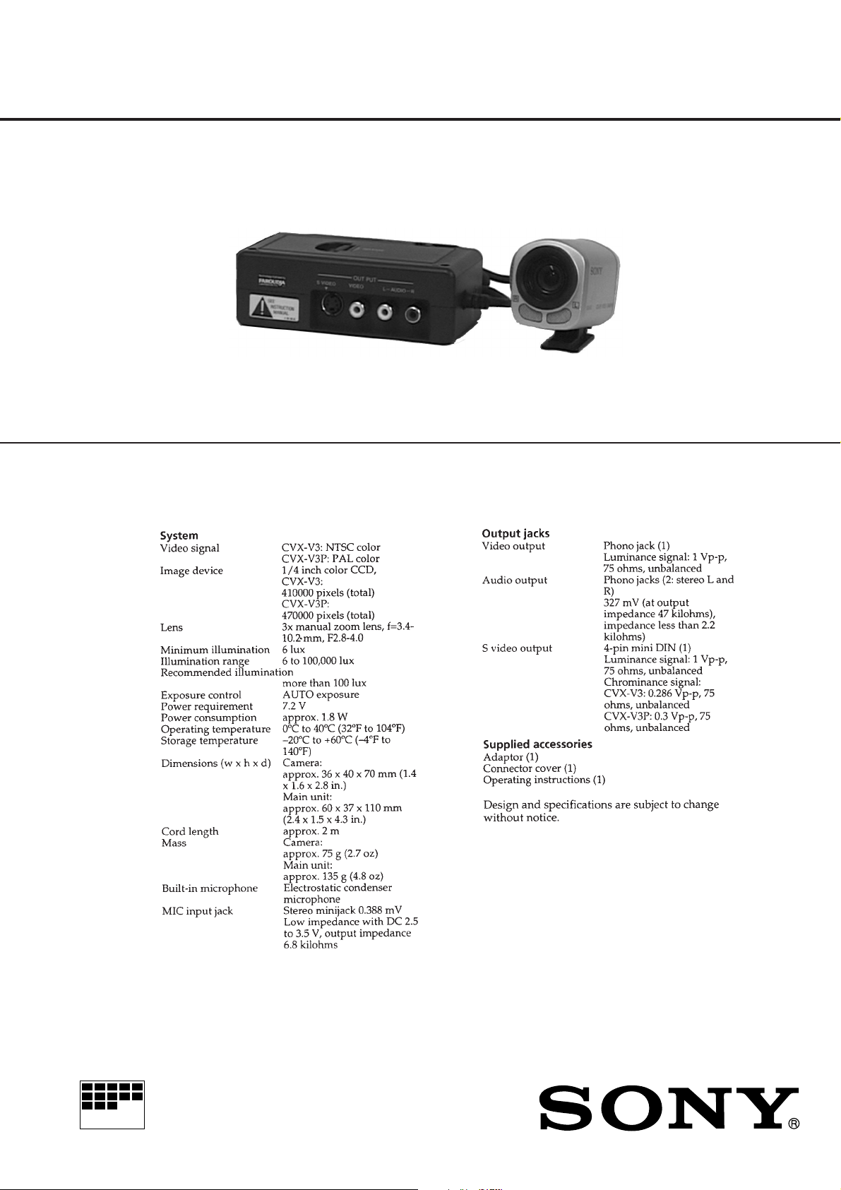
Photo: CVX-V3
NTSC model: CVX-V3
PAL model : CVX-V3P
SPECIFICATIONS
US Model
Canadian Model
CVX-V3
AEP Model
UK Model
CVX-V3P
MICROFILM
COLOR VIDEO CAMERA
Page 2
CVX-V3/V3P
4-2. PRINTED WIRING BOARDS AND SCHEMATIC DIAGRAMS
THIS NOTE IS COMMON FOR WIRING BOARDS AND SCHEMATIC DIAGRAMS
(In addition to this, the necessary note is printed in each block)
(For printed wiring boards)
• b: Pattern from the side which enables seeing.
(The other layers' patterns are not indicated.)
• Through hole is omitted.
• Circled numbers refer to waveforms.
• There are few cases that the part printed on diagram
isn’t mounted in this model.
• Chip parts.
C
BE
56
123
4
Transistor
6
54
321
4
321
2
5
1
543
3
2
Diode
3
1
2
132
1
(For schematic diagrams)
• All capacitors are in µF unless otherwise noted. pF : µ
µF . 50V or less are not indicated except for electrolytics
and tantalums.
• Chip resistors are 1/10W unless otherwise noted.
kΩ=1000Ω, MΩ=1000kΩ.
• Caution when replacing chip parts.
New parts must be attached after removal of chip.
Be careful not to heat the minus side of tantalum
capacitor, Because it is damaged by the heat.
• Some chip part will be indicated as follows.
Example C541 L452
22U 10UH
TA A 2520
Kinds of capacitor
Temperature characteristics
External dimensions (mm)
• Constants of resistors, capacitors, ICs and etc with XX
indicate that they are not used.
In such cases, the unused circuits may be indicated.
• Parts with ★ differ according to the model/destination.
Refer to the mount table for each function.
• All variable and adjustable resistors have characteristic
curve B, unless otherwise noted.
• Signal name
XEDIT→ EDIT PB/XREC → PB/REC
• 2: non flammable resistor
• 1: fusible resistor
• C: panel designation
• A: B+ Line *
• B: B– Line *
• J : IN/OUT direction of (+,–) B LINE. *
• C: adjustment for repair. *
• Circled numbers refer to waveforms. *
* Indicated by the color red.
Note : Les composants identifiés par une marque
! sont critiques pour la sécurité.
Ne les remplacer que par une pièce portant
le numéro spécifie.
(Measuring conditions voltage and waveform)
• Voltages and waveforms are measured between the
measurement points and ground when camera shoots
color bar chart of pattern box. They are reference values
and reference waveforms. *
(VOM of DC 10 MΩ input impedance is used.).
• Voltage values change depending upon input impedance
of VOM used.)
1. Connection
Pattern box
Front side of the lens
L = About 40 cm
2. Adjust the distance so that the output waveform of Fig.
a and the Fig. b can be obtain.
Yellow
Cyan
AABBA=B
Fig. a (Video output terminal output waveform)
Cyan
White
Green
Yellow
Fig.b (Picture on monitor TV)
When indicating parts by reference number, please
include the board name.
L
H
White
Green
Red
Magenta
Magenta
Red
Blue
Blue
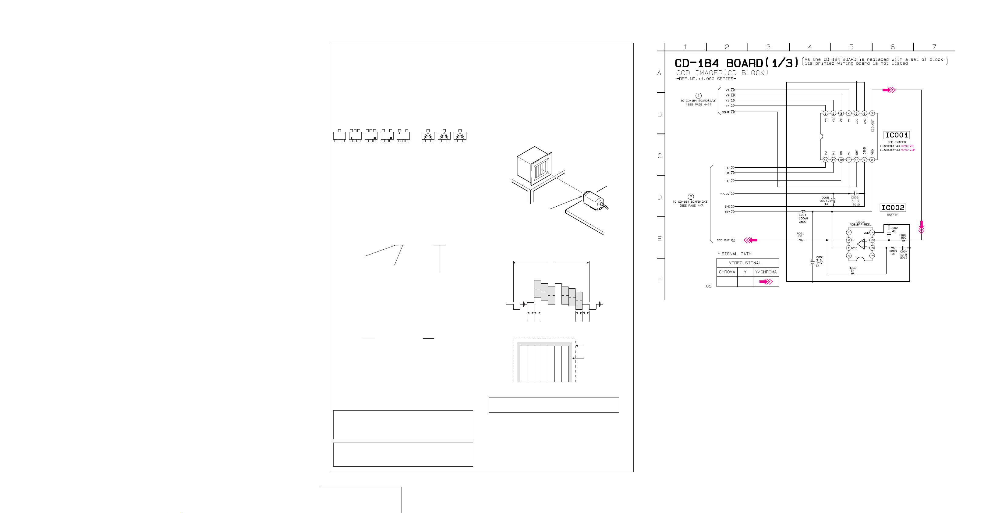
CD-184 (CCD IMAGER) SHEMATIC DIAGRAM
Electron beam
scanned frame
CRT picture frame
Note : The components identified by mark ! or
dotted line with mark ! are critical for safety.
Replace only with part number specified.
CCD IMAGER
CD-184 (1/3)
4-5 4-6
Page 3
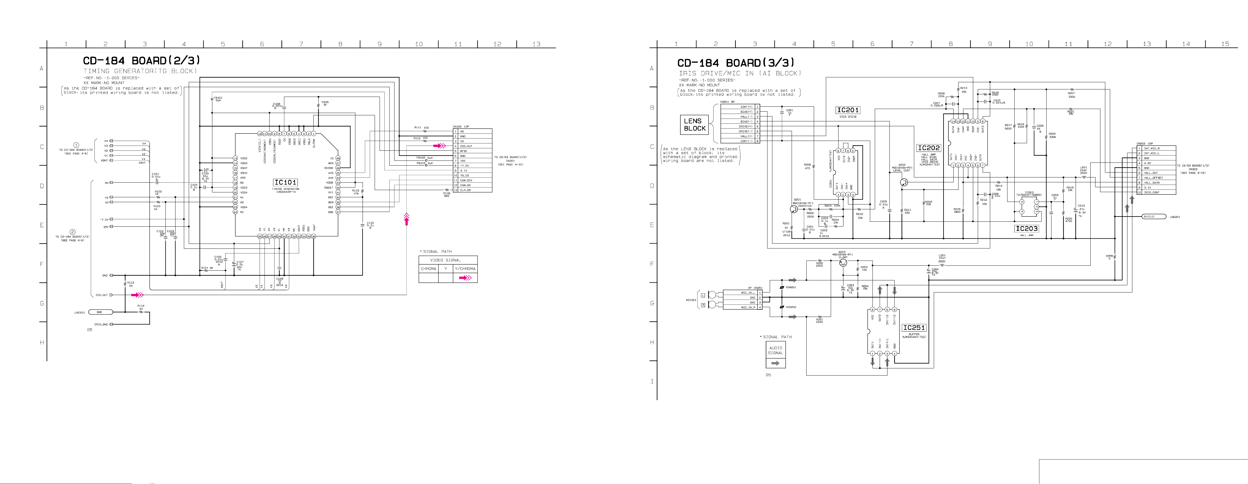
CD-184 (TIMING GENERATOR), (IRIS DRIVE, MIC IN) SCHEMATIC DIAGRAMS
CVX-V3/V3P
4-7 4-8 4-9
4-10
TIMING GENERATOR / IRIS DRIVE, MIC IN
CD-184 (2/3) CD-184 (3/3)
Page 4

CS-53 (CAMERA, Y/C PROCESS) SCHEMATIC DIAGRAM
CS-53 BOARD (1/3)
1
CVX-V3/V3P
6
1.8 Vp-p
14.318 MHz: NTSC
14.187 MHz: PAL
IC304 !¡
2
0.8 Vp-p
28.636 MHz
7
IC304 5
3
0.8 Vp-p
28.636 MHz: NTSC
28.375 MHz: PAL
8
IC304 4
4
0.9 Vp-p
14.318 MHz: NTSC
14.187 MHz: PAL
9
IC305 !§
5
0.14 usec
IC305 2 – 0
10
3.2 Vp-p
H
IC305 @§
V=60 Hz: NTSC
V
V=50 Hz: PAL
IC307 %¡
H
IC307 @º
H
IC307 @£
PAL
17.734475 MHz
IC307 ^£
1.0 Vp-p
3 Vp-p
0.6 Vp-p
0.9 Vp-p
2.3 Vp-p
NTSC model: CVX-V3
P AL model : CVX-V3P
4-15 4-16 4-17 4-18
CAMERA, Y/C PROCESS
CS-53 (1/3)
Page 5

CVX-V3/V3P
CVX-V3/V3P
CS-53 BOARD (2/3)
11
V
V=60 Hz: NTSC
V=50 Hz: PAL
IC502 ^™
12
32.768 kHz
IC502 %™
13
20 MHz
IC502 $¡
NTSC model: CVX-V3
P AL model : CVX-V3P
CS-53 (MODE CONTROL) SCHEMATIC DIAGRAM • See pag e 4-11 for CS-53 BOARD printed wiring board.
3 Vp-p
0.7 Vp-p
0.2 Vp-p
MODE CONTROL
CS-53 (2/3)
4-20 4-21 4-22
Page 6

CS-53 (MIC AMP) SCHEMATIC DIAGRAM • See page 4-11 for CS-53 BOARD printed wiring board.
CVX-V3/V3P
CVX-V3/V3P
4-23 4-24
MIC AMP
CS-53 (3/3)
Page 7

VA-103 (DC-DC CONVERTER) SCHEMATIC DIAGRAM
CVX-V3/V3P
VA-103 BOARD (1/3)
1
13 Vp-p
2.0 µsec
Q601 C
4-33 4-34 4-35
DC-DC CONVERTER
VA-103 (1/3)
Page 8

CVX-V3/V3P
VA-103 (VIDEO/AUDIO I/O) SCHEMATIC DIAGRAM • See page 4-28 for VA-103 BOARD printed wiring board.
VA-103 BOARD (2/3)
2
0.46 Vp-p
H
IC701 @™
3
0.5 Vp-p
H
IC701 !§
4
1.0 Vp-p
H
IC701 !¢
5
1.8 Vp-p
H
IC701 9
6
2.1 Vp-p
H
IC701 6
7
1.1 Vp-p
H
IC701 #¡
VIDEO/AUDIO I/O
VA-103 (2/3)
4-36 4-37 4-38
Page 9

VA-103 (LANC I/O), IF-69 (INTERFACE) SCHEMATIC DIAGRAMS • See page 4-28 for VA-103 BOARD and IF-69 BOARD printed wiring boards.
CVX-V3/V3P
4-39 4-40 4-41 E
LANC I/O / INTERFACE
VA-103 (3/3) IF-69
 Loading...