

Page 1
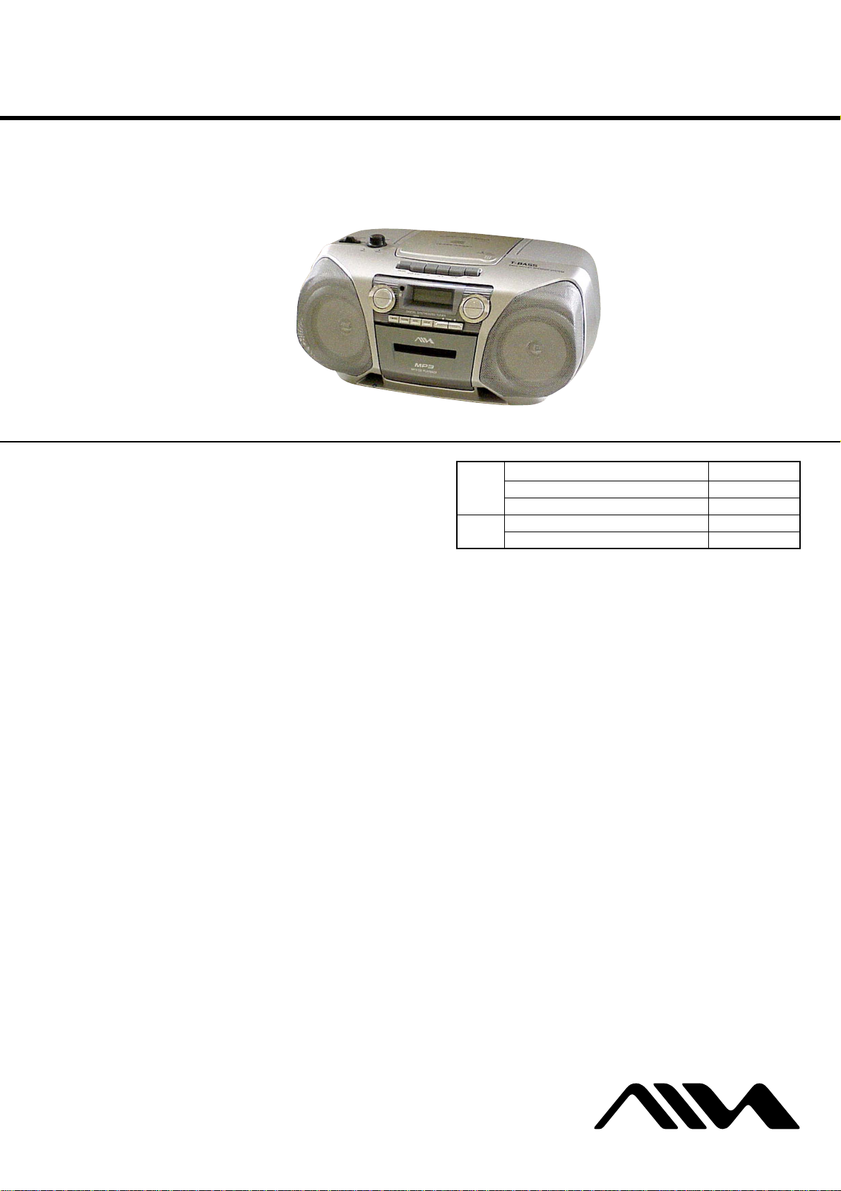
CSD-MP100
SERVICE MANUAL
Ver 1.0 2003. 06
Section
Section
US Model
Canadian Model
AEP Model
UK Model
Australian Model
Model Name Using Similar Mechanism CFD-S200
CD
CD Mechanism Type KSM-213RDP
Optical Pick-up Name KSS-213R
Model Name Using Similar Mechanism NEW
TC
Tape Transport Mechanism T ype MF-MP100
E Model
AUDIO POWER SPECIFICATIONS (US model)
POWER OUTPUT AND TOTAL
HARMONIC DISTORTION
With 8-ohm loads, both channels driven from
150 - 6,300 Hz; rated 1.5 W per channelminimum RMS power, with no more than 10%
total harmonic distortion in AC operation.
Other Specifications
CD player section
System
Compact disc digital audio system
Laser diode properties
Material: GaAlAs
Wave length: 780 nm
Emission duration: Continuous
Laser output: Less than 44.6 µW
(This output is the value measured at a distance of
about 200 mm from the objective lens surface on
the optical pick-up block with 7 mm aperture.)
Spindle speed
200 r/min (rpm) to 500 r/min (rpm) (CLV)
Number of channels
2
Frequency response
20 - 20,000 Hz +1/–2 dB
Wow and flutter
Below measurable limit
SPECIFICATIONS
Radio section
Frequency range
FM: 87.5 - 108 MHz
US, CND model:
AM: 530 - 1,710 kHz
TW, AUS, KR model:
AM: 531 - 1,611 kHz
AEP, UK, E4, E15, SP model:
AM: 531 - 1,611 kHz (9 kHz step)
530 - 1,610 kHz (10 kHz step)
Antennas
FM: Telescopic antenna
AM: Built-in ferrite bar antenna
Cassette-corder section
Recording system
4-track 2 channel stereo
Fast winding time
Approx. 120 sec. with Sony cassette C-60
Frequency response
TYPE I (normal): 80 - 10,000 Hz
– Continued on next page –
9-877-441-01
2003F04-1
© 2003. 06
CD STEREO RADIO CASSETTE RECORDER
Sony Corporation
Personal Audio Company
Published by Sony Engineering Corporation
1
Page 2
CSD-MP100
General
Speaker
Full range: 10 cm dia.,
4 Ω, cone type (2)
Power output
2.0 W + 2.0 W (at 4 Ω, 10%
harmonic distortion)
Power requirements
For CD stereo radio cassette recorder:
US, CND, TW model:
120 V AC, 60 Hz
E4 model
200 - 240 V AC, 50/60 Hz
E15 model
220 - 240 V AC, 50/60 Hz
AEP, UK, AUS, SP model:
230 V AC, 50 Hz
KR model:
220 V AC, 60 Hz
9 V DC, 6 size D (R20) batteries
For remote control:
3 V DC, 2 size AA (R6) batteries
Power consumption
AC 10 W
Battery life
For CD stereo radio cassette recorder:
FM recording
Sony R20P: approx. 13.5 h
Sony alkaline LR20: approx. 24 h
Tape playback
Sony R20P: approx. 7.5 h
Sony alkaline LR20: approx. 15 h
CD playback
Sony R20P: approx. 2.5 h
Sony alkaline LR20: approx. 7 h
Dimensions
Approx. 390 × 170 × 259.5 mm (w/h/d)
3/8 × 6 3/4 × 10 1/4 inches) (incl. projecting parts)
(15
Mass
Approx. 4 kg (8 lb. 13 oz.) (incl. batteries)
Supplied accessories
AC power cord (1)
Remote control (RM-Z1S002) (1)
Design and specifications are subject to change without
notice.
•Abbreviation
CND : Canadian model
E4 : AC 200-240V area in E model
E15 : AC 220-240V area in E model
TW : Taiwan model
AUS: Australian model
SP : Singapore model
KR : Korean model
AEP, UK, E, AUS model
CLASS 1 LASER PRODUCT
LUOKAN 1 LASER LAITE
KLASS 1 LASER APPARAT
This Compact Disc player is classified as a CLASS 1
LASER product.
The CLASS 1 LASER PRODUCT mark is located at the
bottom.
CAUTION
Use of controls or adjustments or performance of procedures other than those specified herein may result in hazardous radiation exposure.
Flexible Circuit Board Repairing
• Keep the temperature of the soldering iron around 270˚C during
repairing.
• Do not touch the soldering iron on the same conductor of the
circuit board (within 3 times).
• Be careful not to apply force on the conductor when soldering
or unsoldering.
Notes on Chip Component Replacement
• Never reuse a disconnected chip component.
• Notice that the minus side of a tantalum capacitor may be dam-
aged by heat.
NOTES ON HANDLING THE OPTICAL PICK-UP BLOCK
OR BASE UNIT
The laser diode in the optical pick-up block may suffer electrostatic
breakdown because of the potential difference generated by the
charged electrostatic load, etc. on clothing and the human body.
During repair, pay attention to electrostatic breakdown and also use
the procedure in the printed matter which is included in the repair
parts.
The flexible board is easily damaged and should be handled with
care.
NOTES ON LASER DIODE EMISSION CHECK
The laser beam on this model is concentrated so as to be focused on
the disc reflective surface by the objective lens in the optical pickup block. Therefore, when checking the laser diode emission,
observe from more than 30 cm away from the objective lens.
SAFETY-RELATED COMPONENT WARNING!!
COMPONENTS IDENTIFIED BY MARK 0 OR DOTTED LINE
WITH MARK 0 ON THE SCHEMATIC DIAGRAMS AND IN
THE PARTS LIST ARE CRITICAL TO SAFE OPERATION.
REPLACE THESE COMPONENTS WITH SONY P ARTS WHOSE
PART NUMBERS APPEAR AS SHOWN IN THIS MANUAL OR
IN SUPPLEMENTS PUBLISHED BY SONY.
ATTENTION AU COMPOSANT AYANT RAPPORT
À LA SÉCURITÉ!!
LES COMPOSANTS IDENTIFIÉS P AR UNE MARQUE 0 SUR LES
DIAGRAMMES SCHÉMA TIQUES ET LA LISTE DES PIÈCES SONT
CRITIQUES POUR LA SÉCURITÉ DE FONCTIONNEMENT. NE
REMPLACER CES COMPOSANTS QUE PAR DES PIÈCES SONY
DONT LES NUMÉROS SONT DONNÉS DANS CE MANUEL OU
DANS LES SUPPLÉMENTS PUBLIÉS PAR SONY.
2
Page 3

CSD-MP100
About “MP3”
What is the MP3
MP3 (MPEG 1 Audio Layer -3) is a standard technology and format
for compressing a sound sequence. The file is compressed to about
1/10 of its original size.
Sounds outside the range of human hearing are compressed while
the sounds we can hear are not compressed.
Playable “MP3” files on the player
You can only play MP3 files recorded by following requirements.
Usable media
CD-Rs and CD-RWs
Usable disc format
You can use ISO 9660 Level 1, Level 2 and Joliet extension format
discs. In some cases, MP3 files that are recorded in a format other
than these formats may not play normally or the file and folder
names may not be displayed correctly.
The major specifications of the usable disc format are as follows:
• Maximum directory steps: 8
• Usable characters for a file/folder name: A - Z, a - z, 0 - 9 and
_ (underscore)
• Maximum number of characters for a file name: 16 (8) including quotation marks and a 3-character extension code
Notes for saving files on the media
When the disc is inserted, the player reads all the files on that disc.
If there are many folders or non-MP3 files on the disc, it may take a
long time for play to begin or for the next MP3 file to start play.
Do not save unnecessary folders or files other than MP3 ones in the
disc to be used for MP3 listening.
We recommend that you do not save other types of files
or unnecessary folders on a disc that has MP3 files.
About “ID3 tag”
ID3 tag is a format for adding certain information (track title, artist
name and album title, etc.) to MP3 files.
This player conforms to Version 1.1 of the ID3 tag information,
“track title”, “artist name” and “album title” can be displayed.
Note
If you use a version other than 1.1, ID3 tag information will not be
displayed correctly.
Notes
•When naming, be sure to add the file extension “mp3” to the file
name.
• If you put the extension “mp3” to a file other than an MP3 file,
the player cannot recognize the file properly and will generate
random noise that could damage your speaker.
•The file name does not correspond to the ID tag.
The usable number of folders/files
• Maximum number of folders and files: 512 (in total)
Settings for compression software and writing software
•To compress a source for an MP3 file, we recommend setting
the transfer bit rate of the compression software to “44.1 kHz”,
“128 kbps” and “Constant Bit Rate”.
•To record up to the maximum capacity, set to the “halting of
writing”.
•To record at one time up to the maximum capacity on media that
has nothing recorded it, set to “Disc at Once”.
3
Page 4

CSD-MP100
TABLE OF CONTENTS
1. SERVICING NOTES......................................................... 5
2. GENERAL............................................................................ 6
3. DISASSEMBLY
3-1. Cabinet Rear Assy............................................................... 9
3-2. Chassis CD Assy ................................................................. 9
3-3. Main Board, Tape Board ................................................... 10
3-4. Tape Mechanism Deck ...................................................... 10
3-5. Cassette Lid Assy .............................................................. 11
3-6. Display Board ...................................................................11
3-7. CD Block Assy.................................................................. 12
3-8. CD/MP3 Board ................................................................. 12
3-9. Optical Pick-up ................................................................. 13
3-10. Tuner Board....................................................................... 13
3-11. Power Trans Board ............................................................ 14
3-12. HRP301, HE301, Pinch Roller Arm Assy ......................... 14
3-13. M301, Belt ........................................................................ 15
4. MECHANICAL ADJUSTMENTS............................... 16
5. ELECTRICAL ADJUSTMENTS
Tape Section .......................................................................... 16
Tuner Section......................................................................... 17
CD Section ............................................................................ 18
6. DIAGRAMS
6-1. IC Pin Description............................................................. 19
6-2. Block Diagram – CD Section –......................................... 23
6-3. Block Diagram – Main Section –...................................... 24
6-4. Circuit Boards Location .................................................... 25
6-5. Printed Wiring Board – CD Section – ............................... 26
6-6. Schematic Diagram – CD Section –.................................. 28
6-7. Printed Wiring Board – Tuner Section – ........................... 29
6-8. Schematic Diagram – Tuner Section –.............................. 30
6-9. Printed Wiring Board – Main Section – ............................ 31
6-10. Schematic Diagram – Main Section (1/2) – ...................... 32
6-11. Schematic Diagram – Main Section (2/2) – ...................... 33
6-12. Printed Wiring Board – Tape Section – ............................. 34
6-13. Schematic Diagram – Tape Section – ............................... 35
6-14. Printed Wiring Board – Display Section – ........................ 36
6-15. Schematic Diagram – Display Section –........................... 37
6-16. Printed Wiring Boards – Power Supply Section – ............ 38
6-17. Schematic Diagram – Power Supply Section –................. 40
6-18. IC Block Diagrams............................................................ 41
7. EXPLODED VIEWS
7-1. Main Board Section .......................................................... 44
7-2. Cabinet Front (1) Section .................................................. 45
7-3. Cabinet Front (2) Section .................................................. 46
7-4. Chassis CD Section ........................................................... 47
7-5. Cabinet Rear Section......................................................... 48
7-6. Tape Mechanism Section .................................................. 49
7-7. CD Mechanism Section .................................................... 50
8. ELECTRICAL PARTS LIST......................................... 51
4
Page 5
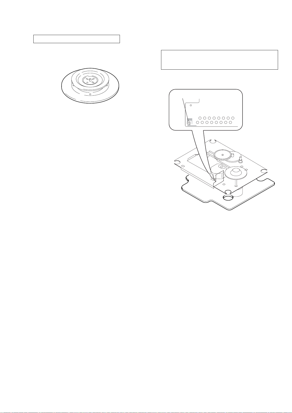
SECTION 1
solder
SERVICING NOTES
CSD-MP100
CHUCK PLATE JIG ON REPAIRING
On repairing CD section, playing a disc without the lid (CD), use
Chuck Plate Jig.
• Code number of Chuck Plate Jig: X-4918-255-1
PRECAUTION TO REPLACE OPTICAL BLOCK
(KSM-213RDP)
Body or clothes electrostatic potential could ruin laser diode
in the optical block. Be sure ground body and workbench,
and use care the clothes do not touch the diode.
1) After the connection, remove solder shown in the right figure.
5
Page 6
CSD-MP100
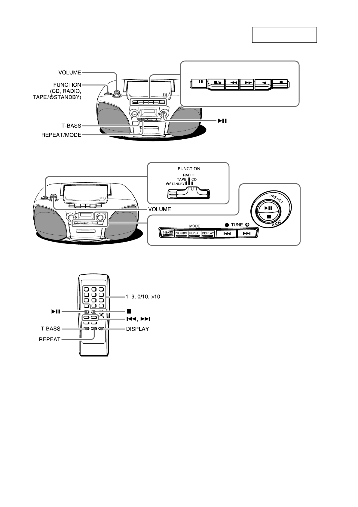
SECTION 2
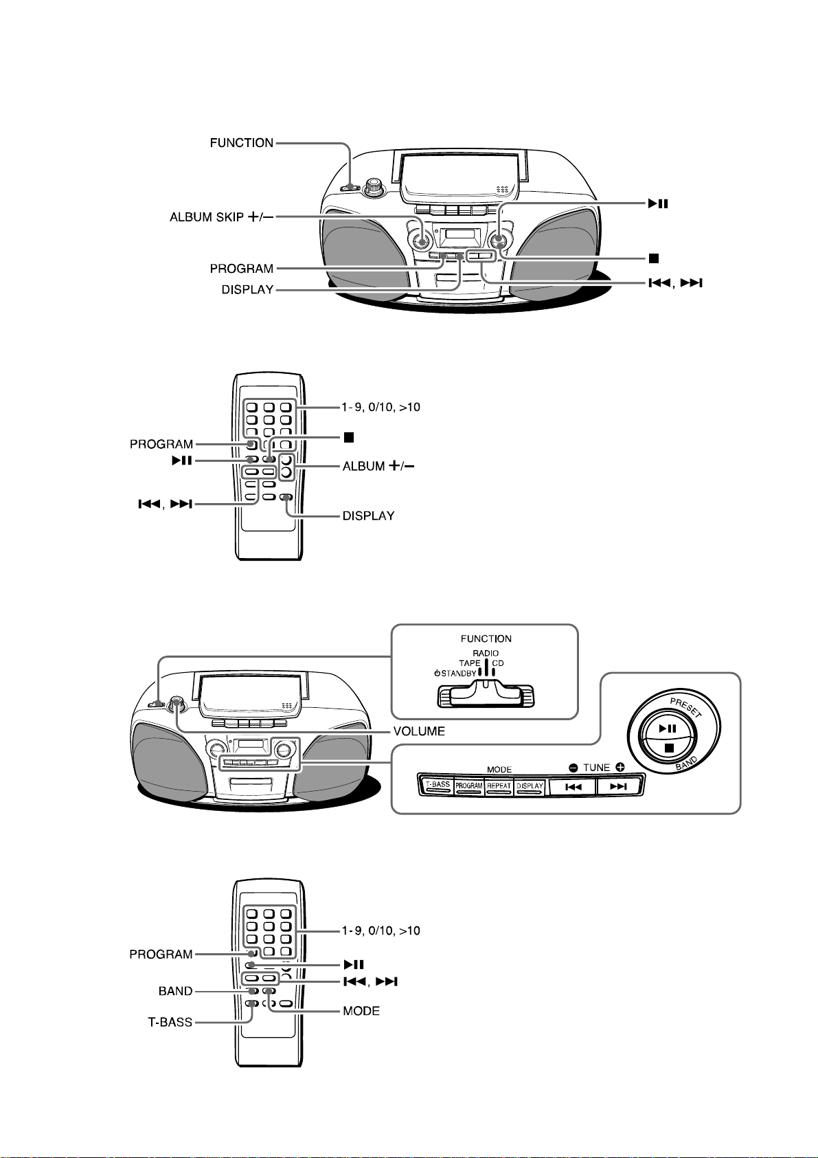
GENERAL
This section is extracted
from instruction manual.
PAUSE
STOP/EJECT
FF REW PLAY
REC
6
Page 7
CSD-MP100
7
Page 8
CSD-MP100
SECTION 3
DISASSEMBLY
• The equipment can be removed using the following procedure.
SET
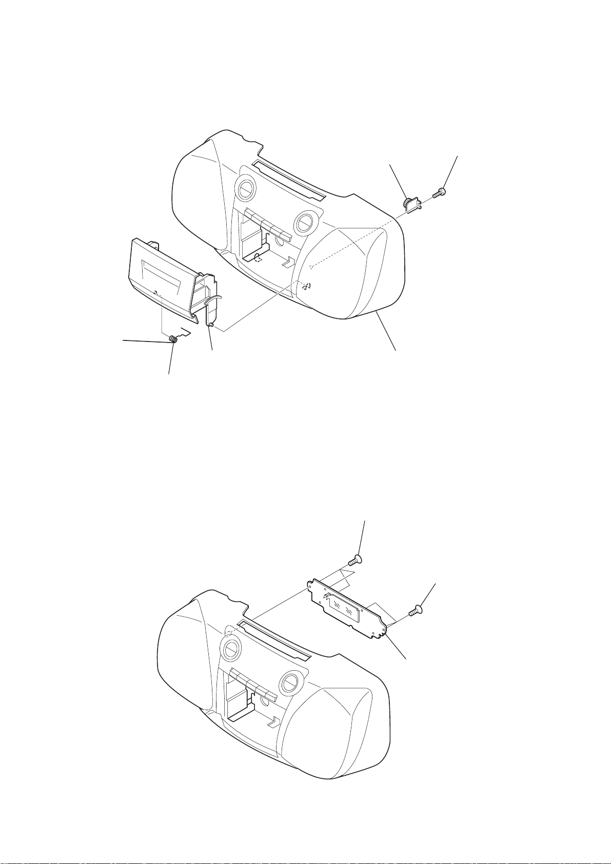
3-1. CABINET REAR ASSY
(Page 9)
3-2. CHASSIS CD ASSY
(Page 9)
3-3. MAIN BOARD,
TAPE BOARD
(Page 10)
3-4. TAPE MECHANISM DECK
(Page 10)
3-5. CASSETTE LID ASSY
(Page 11)
3-6. DISPLAY BOARD
(Page 11)
3-10. TUNER BOARD
(Page 13)
3-7. CD BLOCK ASSY
(Page 12)
3-8. CD/MP3 BOARD
(Page 12)
3-9. OPTICAL PICK-UP
(Page 13)
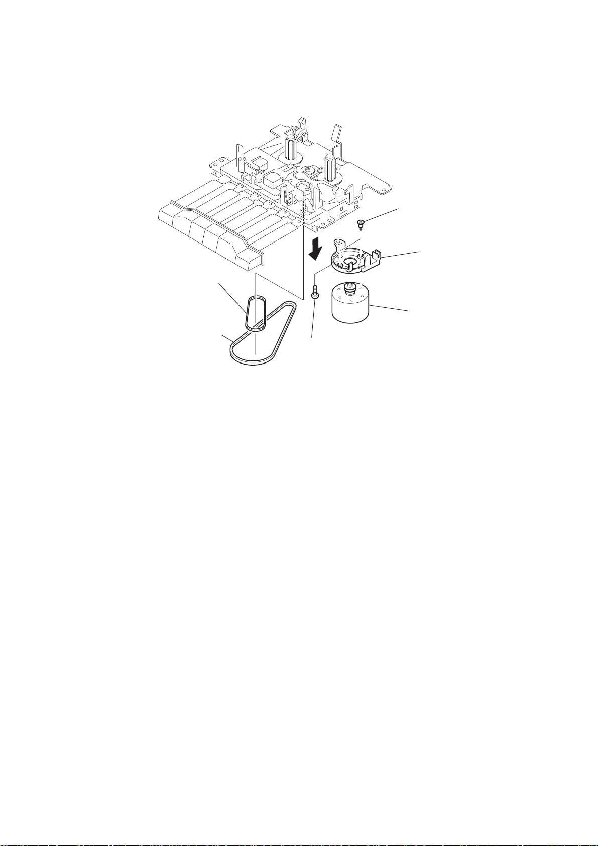
3-13. M301, BELT
(Page 15)
3-11. POWER TRANS BOARD
(Page 14)
3-12. HRP301, HE301,
PINCH ROLLER ARM ASSY
(Page 14)
8
Page 9
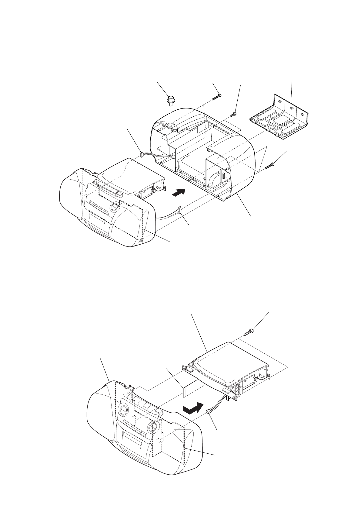
Note : Follow the disassembly procedure in the numerical order given.
)
3-1. CABINET REAR ASSY
4
1
knob RTRY VOL
7
CN101
6
two
BVTP 3 x 25
(+
screws
CSD-MP100
2
)
3
two
screws
BVTP 3 x 10
(+
)
cover (BATT)
5
three
(+
BVTP 3 x 25
screws
)
3-2. CHASSIS CD ASSY
cabinet front assy
2
CN401
(flat type)
8
CNP1
MAIN board
5
chssis CD assy
9
cabinet rear assy
3
two
screws
BVTP 3 x 10
(+
4
1
CN604
MAIN board
9
Page 10
CSD-MP100
)
)
3-3. MAIN BOARD, TAPE BOARD
qs
two
holders (PWB)
7
1
CN201
8
CN301
6
screw
(+
3
CN601
(flat type)
BVTP 3 x 10
qa
two
(+
4
CN603
(flat type)
)
5
CN602
(flat type)
0
Removal the solders.
screws
BVTP 2.6 x 10
2
CN302
9
(+
qf
)
two
screws
BVTP 2.6 x 10
MAIN board
3-4. TAPE MECHANISM DECK
cabinet front assy
qd
TAPE board
3
two
(+
BVTP 2.6 x 10
screws
2
two
(+
BVTP 2.6 x 10
)
screws
10
1
4
tape mechanism deck
Page 11
3-5. CASSETTE LID ASSY
)
)
2
damper
1
screw
(+
BVTP 2.6 x 10
CSD-MP100
4
3-6. DISPLAY BOARD
3
cassette lid assy
cassette spring T
cabinet front assy
2
three
(+
screws
KTP 3 x 10
)
1
three
(+
screws
KTP 3 x 10
3
DISPLAY board
11
Page 12
CSD-MP100
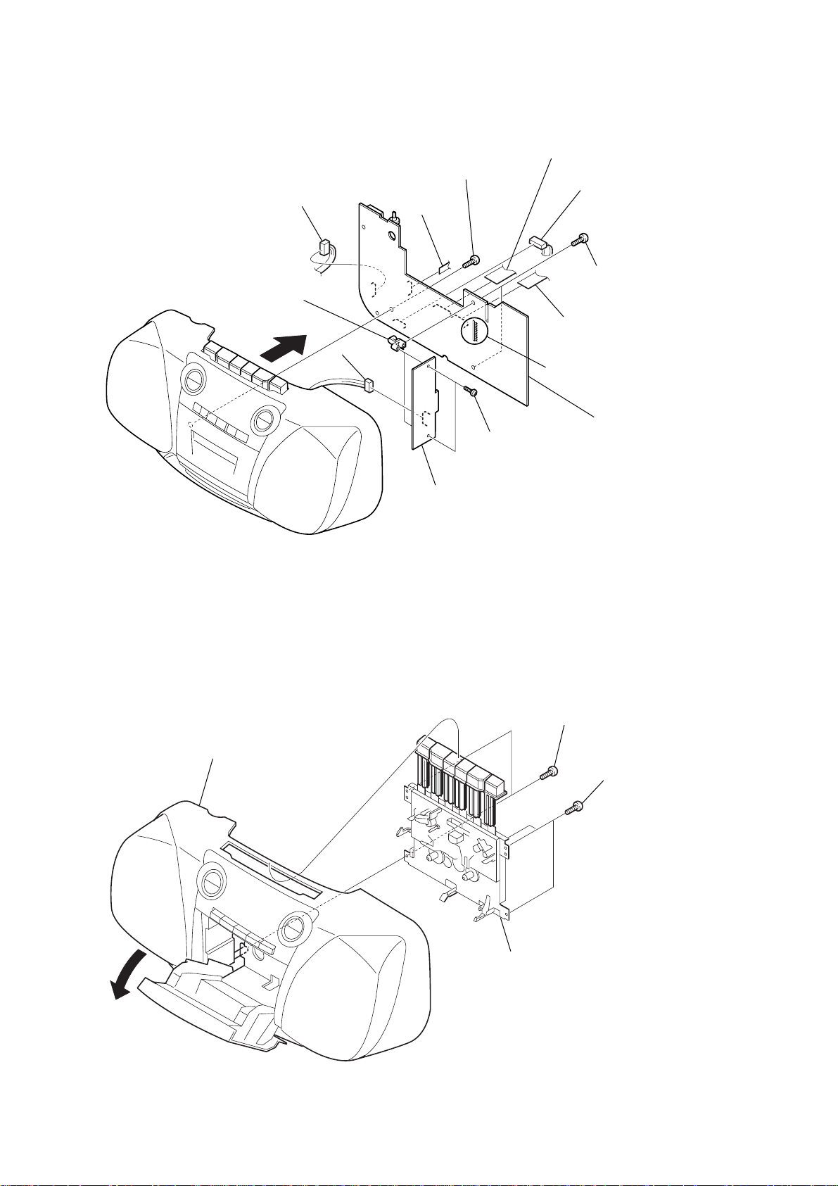
3-7. CD BLOCK ASSY
4
two vibration proof rubbers
two claws
chassis CD assy
3
CD cover
two claws
3-8. CD/MP3 BOARD
2
(
two
screws
2.6 x 10
5
two vibration proof rubbers
)
6
CD block assy
1
two
(
2.6 x 10
CD mechanism
screws
)
12
4
connector
1
(+
screw
3
2
Remove the two solderings of motor.
BVTT 2 x 6
Remove the two solderings of motor.
5
CD/MP3 board
)
Page 13
3-9. OPTICAL PICK-UP
)
3
screw
PWB tapping (M2)
(+
5
sled shaft
CSD-MP100
6
optical pick-up
claw
1
gear (A)
4
)
2
screw
PWB tapping (M2)
(+
)
3-10. TUNER BOARD
3
screw
(+
BVTP 3 x 10
holder (PWB TU)
)
5
6
TUNER board
2
telescopic antenna
1
(+
screw
B 2.6 x 10
4
two claws
13
Page 14
CSD-MP100
y
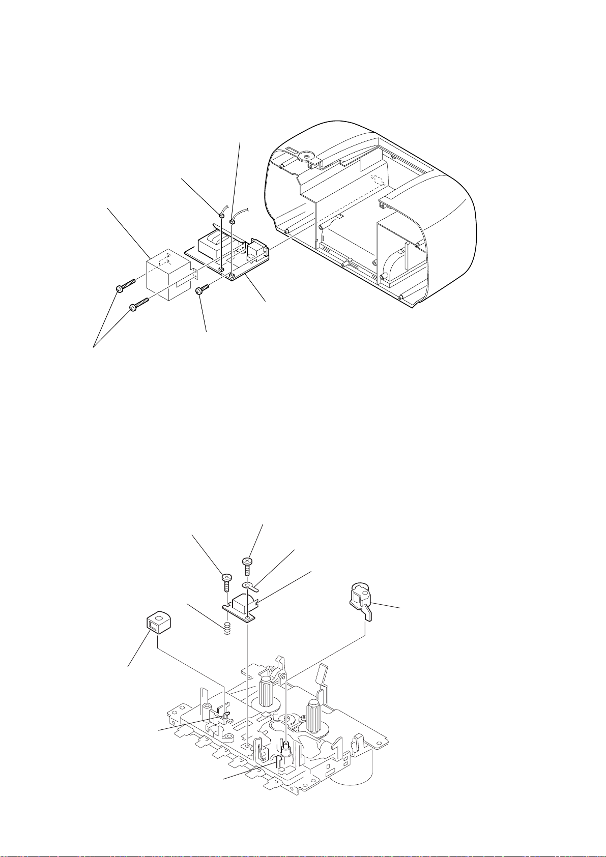
3-11. POWER TRANS BOARD
4
transformer shield
2
CN103
1
CN102
6
POWER TRANS board
5
two
screws
3
four
BVTP 3 x 20
(+
screws
)
(screw (2.6))
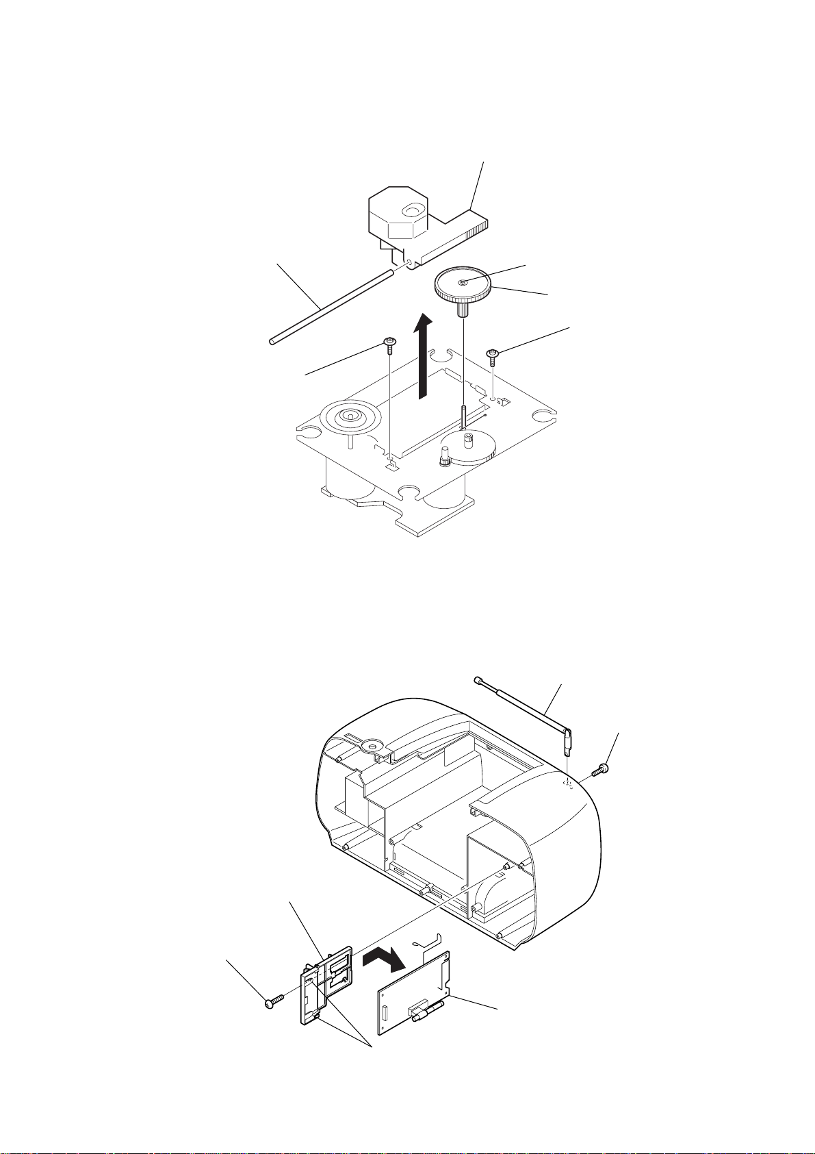
3-12. HRP301, HE301, PINCH ROLLER ARM ASSY
5
screw
(azimuth)
7
azimuth spring
3
screw
(+B bind)
4
lug plate
6
HRP301 (REC/PB head)
1
pinch roller arm ass
14
2
HE301
(ERASE head)
claw
claw
Page 15
3-13. M301, BELT
4
main belt
3
RF belt
2
1
screw (MB)
5
two
screws
(motor coller)
motor bracket
6
M301
(sub motor assy)
CSD-MP100
15
Page 16
CSD-MP100
SECTION 4
MECHANICAL ADJUSTMENTS
SECTION 5
ELECTRICAL ADJUSTMENTS
PRECAUTION
1. Clean the following parts with a denatured-alcohol-moistened
swab :
record/playback head pinch roller
erase head rubber belts
capstan idlers
2. Demagnetize the record/playback head with a head demagnetizer. (Do not bring the head magnetizer close to the erase head.)
3. Do not use a magnetized screwdriver for the adjustments.
4. The adjustments should be performed with the rated power
supply voltage (9V) unless otherwise noted.
Torque Measurement
Mode Torque meter Meter reading
2.95 – 6.86 mN • m
FWD CQ-102C (30 – 70 g • cm)
(0.42 – 0.97 oz • inch)
FWD
Back Tension
FF CQ-201B (more than 60 g • cm)
REW CQ-201B (more than 60 g • cm)
CQ-102C (1.5 – 5.5 g • cm)
0.15 – 0.53 mN • m
(0.021 – 0.076 oz • inch)
more than 5.88 mN • m
(more than 0.83 oz • inch)
more than 5.88 mN • m
(more than 0.83 oz • inch)
TAPE SECTION 0 dB = 0.775 V
• Standard Output Level
Output terminal SPEAKER L-CH (SP301)
load impedance 8 Ω
output signal level 0.25 V (–10 dB)
• Test T ape
Type Signal Used for
WS-48A 3 kHz, 0 dB tape speed adjustment
Tape Speed Adjustment
Procedure:
Mode: playback
test tape
WS-48A
(3 kHz, 0 dB)
set
SPEAKER, L-CH (SP301)
Adjust so that the value on the digital frequency counter is
3,000 Hz.
digital frequency
counter
4
Ω
Tape Tension Measurement
Mode Tension meter Meter Reading
FWD CQ-403A
more than 100 g
(more than 3.53 oz)
Specification Value:
Digital frequency counter
2,940 to 3,060 Hz
Adjust so that the frequency at the beginning and that at the end of
tape winding are between 2,970 to 3,030 Hz.
Adjustment Location:
16
Tape speed adjustment
control inside motor
Page 17
CSD-MP100
)
TUNER SECTION 0 dB = 1 µV
• FM Section
Setting:
BAND button: FM
FM RF signal
generator
TP (FM IN)
0.01
µ
F
75 kHz frequency
deviation by 1 kHz signal
output level : as low as possible
• AM Section
Setting:
BAND button: AM
AM RF signal
generator
30% amplitude
modulation by
400 Hz signal
• Connecting Level Meter (FM and AM)
Put the lead-wire
antenna close to
the set.
level meter
(range: 0.5–5 V ac
4
Ω
set
FM IF ADJUSTMENT
Adjust for a maximum reading on level meter.
T2
10.7 MHz
FM FREQUENCY COVERAGE
ADJUSTMENT
Frequency Display 87.5 MHz 108 MHz
Reading on Digital voltmeter 1.3 ± 0.3 V 3.0 ± 0.2 V
Adjustment Part <confirmation> L2
FM TRACKING ADJUSTMENT
Adjust for a maximum reading on level meter.
L1 CT1
87.5 MHz 108 MHz
AM IF ADJUSTMENT
Adjust for a maximum reading on level meter.
T1
450 kHz
AM FREQUENCY COVERAGE
ADJUSTMENT
530 kHz 1,710 kHz
Frequency Display
(US, CND) (US, CND)
531 kHz 1,611 kHz
(Except US, CND) (Except US, CND)
Reading on
Digital voltmeter
1.0 ± 0.05 V 5.3 ± 0.7 V
Adjustment Part L4 <confirmation>
set
SPEAKER, L-CH (SP301)
• Connecting Digital Voltmeter (FM and AM)
digital
voltmeter
100 kΩ
TP (VT)
•Repeat the procedures in each adjustment several times, and the
frequency coverage and tracking adjustments should be finally
done by the trimmer capacitors.
AM TRACKING ADJUSTMENT
Adjust for a maximum reading on level meter.
L3 CT3
620 kHz (US, CND) 1,400 kHz (US, CND)
621 kHz (Except US, CND) 1,404 kHz (Except US, CND)
Adjustment Location: See page 18.
17
Page 18
CSD-MP100
Q701
3
R
7
IC
Adjustment Location:
– MAIN board (component side) –
TP (FM IN)
(CONDUCTOR SIDE)
T1
AM
IF
ADJUSTMENT
FM
ADJUSTMENT
T2
IF
T1
T2
L1
L3
CT1
IC1
CT1, L1
FM
TRACKING
ADJUSTMENT
L2
L2
FM
FREQUENCY
COVERAGE
ADJUSTMENT
CT3, L3
AM
TRACKING
ADJUSTMENT
CT3
L4
TP (VT)
(CONDUCTOR SIDE)
L4
AM
FREQUENCY
COVERAGE
ADJUSTMENT
IC2
CD SECTION
CD section adjustments are done automatically in this set.
In case of operation check, confirm that focus bias.
FOCUS BIAS CHECK
1. Connect the oscilloscope between IC701 pin 4 and pin qa (or
TP (RF) and TP (VREF)).
2. Insert the disc (YEDS-18). (Part No. : 3-702-101-01)
3. Press the N X (CD) button.
4. Confirm that the oscilloscope waveform is as shown in the
figure below. (eye pattern)
A good eye pattern means that the diamond shape ( ) in the
center of the waveform can be clearly distinguished.
• RF signal reference waveform (eye pattern)
VOLT/DIV : 50 mV (10 : 1 probe in use)
TIME/DIV : 500 nS
When observing the eye pattern, set the oscilloscope for AC range
and raise vertical sensitivity.
RF level :
0.85 ± 0.2 Vp-p
Test Point:
— CD/MP3 board (side B) —
R724
C746
C717
C716
C718
R745
R723
C763
C742
C721
C719
C720
R755
C744
C743
C705
R708
R710
R709
C711
R711
R759
C712
TP
(RF)
C710
C707
R764
R726
C708
R727
R730
C713
TP
(VREF)
R729
C706
R725
R763
C709
C740
R728
C714
C701
C715
C
C761
R7
R73
C762
701
18
Page 19
CSD-MP100
SECTION 6
DIAGRAMS
6-1. IC PIN DESCRIPTIONS
• IC1001 LC78684E (MP3 DECODER, CD-ROM DECODER, ANTI-SHOCK CONTROLLER) (CD/MP3 BOARD)
Pin No. Pin Name I/O Pin Description
1 LRSY I CD L/R clock input
2 ADDATA O Audio data output
3 ADBCK O Audio bit clock output
4 ADLRCK O Audio L/R clock output
5 C2FIN I CD C2 error flag input
6 VSS — Ground
7 CKIN I System clock (16.9344 MHz) input
8 VSS — Ground
9CKOUT O Clock (384Fs) output for external DF/DAC.
10 VSS — Ground
11 DVDD1 — Digital power supply pin for I/O.
12 PW I CD subcode data serial input
13 SBSY I CD subcode block synchronized signal input
14 SFSY I CD subcode frame synchronized signal input
15 SBCK O Serial clock output for CD subcode transfer. (Not used. (Open))
16 AVDD — Analog (PLL) power supply pin
17 VPRFR — VCO oscillation range setting pin
18 VCOC I VCO control voltage input
19 VPDO O VCO charge pump output
20 AVSS — Analog ground
21 DVDD2 — Power supply pin for internal logic.
22 VSS — Ground
23 to 30 MDATA0 to 7 I/O DRAM data bus 0 to 7
31 DVDD3 — Digital power supply pin for I/O.
32 VSS — Ground
33 to 40 MDATA8 to 15 I/O DRAM data bus 8 to 15
41 RASB O Row Address Strobe signal output (L: active)
42 WEB O Data Write Enable signal output (L: active)
43 CASLB O Column Address Strobe signal output (for lower byte, L: active)
44 CASUB O Column Address Strobe signal output (for upper byte, L: active)
45 OEB O Output enable signal output (L: active)
46 to 49 MADRS12 to 9 O DRAM address output 12 to 9 (Not used. (Open))
50 MADRS8 O DRAM address output 8
51 DVDD4 — Digital power supply pin for I/O.
52 VSS — Ground
53 to 60 MADRS7 to 0 O DRAM address output 7 to 0
61 DVDD5 — Power supply pin for internal logic.
62 VSS — Ground
63 STREQ I/O
64 STCK I/O MP3 data transfer clock input/DRAM data transfer clock output (Not used. (Open))
65 STDAT I/O MP3 data serial input/DRAM data serial output (Not used. (Open))
66 FSYNC O MP3 frame synchronized signal input (H: active) (Not used. (Open))
67 CRCF O
68 DVDD6 — Power supply pin for internal logic.
69 VSS — Ground
70 WOK I
MP3 data request flag output (H: active)/DRAM data request flag input (H: active)
(Not used. (Open))
CDROM-CRC flag output (H: active)/DRAM data output enable signal output
(H: active) (Not used. (Open))
DRAM write OK input (at CD-DA, H: active)/DRAM data request flag input
(at CD-ROM, H: active)
19
Page 20

CSD-MP100
Pin No. Pin Name I/O Pin Description
71 CNTOK O
72 OVF O
73 CMDOUT O Command serial data output (Nch open drain output pin)
74 CMDIN I Command serial data input
75 CL I Command serial clock input
76 CE I Command enable input (H: active)
77 INTB O Interrupt signal output (L: active)
78 RESB I System reset input (L: active)
79 DATAIN I CD serial data input
80 DATACK I CD bit clock input
Data connecting point detection completion flag output (at CD-DA, H: active)/DRAM
data serial output (at CD-ROM, H: active) (Not used. (Open))
DRAM write discontinue flag output (at CD-DA, H: active)/DRAM data transfer
clock output (at CD-ROM, H: active) (Not used. (Open))
20
Page 21

• IC601 LC877480B-51F5-E (SYSTEM CONTROL) (MAIN BOARD)
Pin No. Pin Name I/O Pin Description
1 CQ-WRQ I CD write request data input
2 MP3-INTB I MP3 interrupt signal iput
3 CD-DO O CD data output
4 CD-DI I CD data input
5 CD-CL O CD clock output
6 MP3-CMDOUT O MP3 command serial data output
7 MP3-CMDIN I MP3 command serial data input
8MP3-CL O MP3 command serial clock output
9MP3-CE O MP3 command chip enable output
10 CD-CE O CD chip enable output
11 I-RES I CPU reset input
12 XT1 I Crystal oscillator (32.768 kHz) input
13 XT2 O Crystal oscillator (32.768 kHz) output
14 VSS1 — Ground
15 CF1 I Ceramic oscillator (4.19 MHz) input
16 CF2 O Ceramic oscillator (4.19 MHz) output
17 VDD1 — Power supply pin (+3.3 V)
18 O-CLKSFT O CPU main clock shift output
19 BATT-CHK-1 I Battery check input
20 BATT-CHK-2 I Battery check input
21 BATT-CHK-3 I Battery check input
22 SDA O EEPROM data output
23 SCL O EEPROM clock output
24 I-MATRIX I Tuner select matrix input
25 I-AC/DC I AC/DC discrimination signal input
26 R-MUTE O Tuner IF mute signal output
27 I-HOLD I Hold mode detection signal input
28 CD-TEST I CD test mode discrimination signal input
29 I-REM I Remocon data input
30 I-BEAT I AM beat select detection signal input
31 R-COUNT I Tuner data input
32 R-CLK O Tuner clock output
33 R-DATA O Tuner data output
34 R-CE O Tuner chip enable output
35 (NCO) O Not used. (Open)
36 O-BEAT1 O AM beat select signal output
37 O-BEAT2 O AM beat select signal output
38 to 45 (NCO) — Not used. (Open)
46 CD — Not used. (Open)
47 RMC I Remocon select signal input
48 I-TAPE I Tape play mode detection signal input
49 CD-DOOR I CD door OPEN/CLOSE detection signal input
50 SEG1 O LCD segment data output
51 SEG2 O LCD segment data output
52 SEG3 O LCD segment data output
53 SEG4 O LCD segment data output
54 VDD2 — Power supply pin (+3.3 V)
55 VSS2 — Ground
56 SEG5 O LCD segment data output
57 SEG6 O LCD segment data output
58 SEG7 O LCD segment data output
59 SEG8 O LCD segment data output
CSD-MP100
21
Page 22

CSD-MP100
Pin No. Pin Name I/O Pin Description
60 SEG9 O LCD segment data output
61 SEG10 O LCD segment data output
62 SEG11 O LCD segment data output
63 SEG12 O LCD segment data output
64 SEG13 O LCD segment data output
65 SEG14 O LCD segment data output
66 SEG15 O LCD segment data output
67 SEG16 O LCD segment data output
68 SEG17 O LCD segment data output
69 SEG18 O LCD segment data output
70 SEG19 O LCD segment data output
71 SEG20 O LCD segment data output
72 SEG21 O LCD segment data output
73 SEG22 O LCD segment data output
74 SEG23 O LCD segment data output
75 SEG24 O LCD segment data output
76 SEG25 O LCD segment data output
77 SEG26 O LCD segment data output
78 SEG27 O LCD segment data output
79 SEG28 O LCD segment data output
80 I-KEY1 I Key input
81 I-KEY2 I Key input
82 (NCO) — Not used. (Open)
83 COM-1 O LCD common data output
84 COM-2 O LCD common data output
85 COM-3 O LCD common data output
86 COM-4 O LCD common data output
87 O-T-BASS O T-BASS control signal output
88 CD-ON O CD power control signal output
89 VSS3 — Ground
90 VDD3 — Power supply pin (+3.3 V)
91 I-CD I CD mode detection signal input
92 I-TU I Tuner mode detection signal input
93 TU-ON O Tuner power control signal output
94 P-CONT O Power supply control signal output
95 O-MUTE O Main mute control signal output
96 MP3-RESB O MP3 reset signal output
97 CD-RES O CD DSP reset signal output
98 (NCO) O Not used. (Open)
99 CD-FSEQ I CD frame synchro detection signal input
100 CD-DRF I CD focus ON detection signal input
22
Page 23

6-2. BLOCK DIAGRAM — CD SECTION —
A
C
B
D
E
F
LD
PD
VREF
OPTICAL PICK-UP
BLOCK
(KSS-213R)
TRACKING
COIL
FOCUS
COIL
M702
SLED
MOTOR
M701
SPINDLE
MOTOR
S701
(LIMIT)
S601
PUSH
OPEN/
CLOSE
M
M
Signal path
: CD
R-ch is omitted due to same as
L-ch.
A
C
B
D
E
F
LD
PD
VR
VREF
T+
T–
F+
F–
SL+
SL–
SP+
SP–
LD POWER
CONTROLLER
Q701
VREF
10
80
79
11
17
18
12
11
26
27
2
1
FIN2
FIN1
7
TIN1
9
TIN2
LDD
LDS
VREF
T+
T–
F+
F–
SL+
SL–
SP+
SP–
SLED/SPINDLE
MOTOR DRIVER,
TRACKING/FOCUS
COIL DRIVER
APC
TRACKING
DRIVE
FOCUS
DRIVE
SLED
MOTOR
DRIVE
SPINDLE
MOTOR
DRIVE
IC702
COIL
COIL
PH/BH
MUTE
VREF
OPIN
TIN
FIN
SLIN
SPIN
CSD-MP100
LCHO
RCHO
DATA
DATACK
LRSY
ASDFIN
ASDACK
ASLRCK
16MOUT
CE
CL
8
MP3-CL
CF2
INTB
MP3-CE
MP3-INTB
11
42
45
59
58
57
56
55
52
50
RESB
962528
MP3-RESB
RESET
AC/DC
HOLD
CONT4
IC601 (1/2)
13
INTERPOLATION
MUTE
&
ATTENUATION
DEEMPHASIS
PLL
VCEC
COMMAND
INTERFACE
RES
DICECL
CD-DO
CD-RES
POWER
SWITCH
Q101,103
CD-CE
RF
48
CONVERTER
TDDTD
20
TD
20
FD
10
7
SL
25
SP
3
23
VREF
15
D/A
FDD
SPDO
21 22 23
FD
SP
3
VREF
SLDO
SL
CD1.8V
EFMIN
AGC
HFL
PH(RFENV)
FE
TE
SLICE
LEVEL
CONTROL
CLV,CAV
CONTROL
A/D
CONVERTER,
SERVO
PROCESSOR
RF AMP,
SYSTEM SERVO PROCESSOR,
DIGITAL SIGNAL PROCESSOR
CD3.3V
+1.8V
REG
IC1003
IC701
49
13
SWITCH
CD-DOOR
U-COM3.3V
88
+3.3V
REG
Q105-108
6.2V
ERROR
CORRECTION
AUDIO CD
FRAME SYNC
DETECT,PROTECT
INSERT
EFM DECODER
GENERAL
PURPOSE
PORT
CONT1
FSEQ
DRF
67
31 72 25 66 63 61 62 49 48
100 99 3 10 5 1 497
CD-DRF
CD-FSEQ
SYSTEM CONTROLLER
CD-ON
VDD(SW)
+6.2V
REG
Q104
+3.3V
REG
IC202
8FS
DIGITAL
FILTER
1-bit DAC
SERIAL
OUT
EXTERNAL
AUDIO IN
WRQ
DO
65 64
CD-DI
CD-CL
CD-WRQ
P-CONT213V206V199V
94
&
CLOCK
GENERATOR
XIN
X701
16.93MHz
BATT
CHECK
3V/6V/9V
CHECK
Q609-612
LPF
XOUT
CMDIN
CMDOUT
67
MP3-CMDIN
FSX/16MIN
MP3-CMDOUT
R-CH
CMDOUT
CMDIN
CL
CE
INTB
RESB
27
RESET
Q601,607
Q608
CD L CH
7960
DATA IN
DATACK
80
1
LRSY
2
ADDATA
3
ADBCK
4
ADLRCK
5
CF2IN
CKOUT
9
CKIN
754
CKIN
754
CKIN
754
CKIN
754
CKIN
754
CMDOUT
73
74
CMDIN
75
CL
76
CE
INTB
77
78
RESB
D101 – 104
1
HOLD
Q602
(Page 24)
MDATA0
I
MDATA15
23-30,33-40 60-53,50
2-5,7-10,
35-38,40-43
DQ0-DQ15
T101
POWER
TRANSFORMER
F101
MPS DECODER,
CD-ROM DECODER,
ANTI-SHOK
CONTROLLER
IC1001
MADRS0
I
MADRS8
18-21,24-28
A0-A8
SDRAM
IC1002
220-240V
110-127V
S102
AC IN VOLTAGE
E MODEL ONLY
OEB
CASLB
CASUB
RASB
41 44 43 45 42
16 30 31 29 15
OE
RAS
LCAS
UCAS
3V
DRY BATTERY
(IEC DESIGNATION R20)
3V
3V
WEB
WE
J101
AC IN
SIZE " D "
6PCS,9V
23 23
Page 24

CSD-MP100
6-3. BLOCK DIAGRAM — MAIN SECTION —
HRP301
RECORD/PLAYBACK
HEAD
REC PB
R-CH
S301H
Q303
Q301
37
BEAT2
S301G
REC PB
PB REC
36
S301F
BEAT1
T301
8
REC/PB PREAMP
IC301
ALC
REC
BIAS
OSC
Q302
SYSTEM CONTROLLER
5
IC601 (2/2)
7
S301I
REC PB
S301E
PB
REC
1
(Page 23)
U-COM3.3V
CD L CH
TAPE
TAPE
CD
S101A
CD
91
S101C
RADIO
RV201
5V REG
D118
VOLUME
Q203
CONTROL
RECEIVER
3
REMOTE
IC801
1
29
REM
LINE
AMP
Q205
6V
RADIO
92
TU
CD
Q201
MUTE
CONTROL
Q209
95
MUTE
POWER AMP
IC201
6 2
87
ASST-B
48
SW9V
TAPE
R-CH
U-COM3.3V
R-CH
MOTOR
DRIVE
Q110,111
SP301
SPEAKER
(L-CH)
SP302
SPEAKER
(R-CH)
M301
CAPSTAN/REEL
MOTOR
M
S302
(TAPE PLAY)
ANT1
FM
TELESCOPIC
ANTENNA
VDD (SW)
XT113XT2
12
X601
32.768kHz
D112
CT3
TRACKING
D3
FERRITE-ROD
ANTENNA
RADIO 6V
CT3,L3
AM
TRACKING
CLKSFT16CF2
18
15
L4
AM
FREQUENCY
COVERAGE
L3
AM
CT1,L1
FM
CF1
X602
4.19MHz
L4
RADIO 6V
AM OSC
AM
RF-IN
22 4 6
FM
RF-IN
2
FM
RF-OUT
RADIO 6V
1 2 3 4
PD
16
LP-IN
17
LP-OUT
18
AM
OSC
AM
MIX
D1 D2
R-CE
3334 32 31
CE
FM
MIX
FM
OSC
2124
R-CLK
R-DATA
DI
CL
AM IN
11 12
1920
FM OSC
R-COUNT
DO
FM IN
OSC-OUT
MIX-OUT
RADIO 6V
93
POWER
SWITCH
6.2V
Q605,606
XOUT
20 19
FM/AM FRONT END, IF AMP,
T1
T1
AM IF
L2
L2L1 CT1
FM
FREQUENCY
COVERAGE
TU-ON
75kHz
FM MPX
IC1
RADIO 6V
FM/AM PLL
XIN
X1
CF4
CF2
RADIO 6V
RADIO 6V
IC2
7
KEY181KEY2
80
KEY NETWORK
S801-810
MO/ST10IF IN
13
14 17 13 18
LPF2/MO-ST
AM
IF-IN
FM
IF-IN
IF
BUFFER
IF-OUT
IF CUT
RADIO 6V
AM
DET
FM
DET
|
SEG1
50 – 54
56 – 79
SEG28
Signal path
BAND8ST-IND
7
ST-IND
LPF1/BAND
R-MUTE
26
COM1|COM4
83 – 86
LIQUID CRYSTAL
DISPLAY PANEL
LCD801
: FM
: AM
AF
BUFFER
DET-OUT
16 15
MPX-IN
FM
MPX
IF CUT
MUTE
R-OUT
L-OUT
11
TU_IN_R
12
: TAPE PLAY
: TAPE REC
: CD
R-ch is omitted due to same as
QUAD
10
T2
T2
FM IF
L-ch.
2424
Page 25

CSD-MP100
6-4. CIRCUIT BOARDS LOCATION
MAIN board
DISPLAY board
POWER TRANS board
TAPE board
SELECTOR board (E4, E15 model)
CD/MP3 board
TUNER board
BATT-2 board
BATT-1 board
• Wavef orms (Mode: PLAY)
— CD/MP3 Board —
500mV/div 0.5µsec/div
1
0.85±0.2Vp-p
IC7014 (RF)
100mV/div 200µsec/div
2
1.8V
Approx. 100mVp-p
IC701qd (FE)
100mV/div 200µsec/div
3
1.8V
Approx. 100mVp-p
IC701qg (TE)
2V/div 0.05µsec/div
4
6Vp-p
16.93MHz
IC701rk (XOUT)
2V/div 50nsec/div
5
• Wavef orm
— TUNER Board —
0.5V/div 5µsec/div
1
75kHz
IC2 w; (XOUT)
• Wavef orms
— MAIN Board —
1V/div 20µsec/div
1
32.768kHz
IC601 qd (XT2)
1V/div 0.2µsec/div
2
4.19MHz
IC601 qh (CF2)
1.5Vp-p
3.1Vp-p
2.9Vp-p
60nsec
IC701 t; (FSX/16MIN (I))
2V/div 50nsec/div
6
60nsec
IC1001 7 (CKIN (I))
6Vp-p
7Vp-p
25 25
Page 26

CSD-MP100
• Refer to page 25 for Circuit Boards Location.
6-5. PRINTED WIRING BOARD — CD SECTION — • Refer to page 26 for Common Note on Printed Wiring Boards.
THIS NOTE IS COMMON FOR PRINTED WIRING
BOARDS AND SCHEMATIC DIAGRAMS.
(In addition to this, the necessary note is
printed in each block.)
Common Note on Schematic Diagrams:
• All capacitors are in µF unless otherwise noted. pF: µµF
50 WV or less are not indicated except for electrolytics
and tantalums.
• All resistors are in Ω and 1/
specified.
f
•
• C : panel designation.
• A : B+ Line.
• H : adjustment for repair.
•Total current is measured with no cassette installed.
•Power voltage is dc 9V and fed with regulated dc power
•Voltages are taken with a VOM (Input impedance 10 MΩ).
•Waveforms are taken with a oscilloscope.
• Circled numbers refer to waveforms.
• Signal path.
•Abbreviation
: internal component.
Note:
The components identified by mark 0 or dotted
line with mark 0 are criti-
cal for safety.
Replace only with part
number specified.
supply from battery terminal.
Voltage variations may be noted due to normal produc-
tion tolerances.
Voltage variations may be noted due to normal production tolerances.
F : FM
f : AM
E : PB
a : REC
J : CD
CND : Canadian model.
E4 : AC 200-240V area in E model.
E15 : AC 220-240V area in E model.
TW : Taiwan model.
AUS: Australian model.
SP : Singapore model.
KR : Korean model.
4
W or less unless otherwise
Note:
Les composants identifiés par
une marque 0 sont critiques
pour la sécurité.
Ne les remplacer que par une
piéce portant le numéro
spécifié.
234567891011
1
A
B
C
D
E
F
Common Note on Printed Wiring Boards:
• X : parts extracted from the component side.
• Y : parts extracted from the conductor side.
• x : parts mounted on the conductor side.
f
•
• : Pattern from the side which enables seeing.
•Abbreviation
: internal component.
CND : Canadian model.
E4 : AC 200-240V area in E model.
E15 : AC 220-240V area in E model.
TW : Taiwan model.
AUS: Australian model.
SP : Singapore model.
KR : Korean model.
G
H
I
J
2626
Page 27

CSD-MP100
A
B
C
D
E
F
G
H
J
1
23456789101112
(Page 31)
• Semiconductor
Location
CNP702
R1074
C1001
R1080
FB1002
R1005
C1066
C760
C767
FB704
R765
C732
C756
R1077
C1074
FB1001
R734
C722
C731
R1068
C737
C734
C1043
R1073
C1044
FB701
C729
C1010
C1011
R713
R1017
R1020
R1081
R1019
X701
C1042
C1012
R1018
IC1001
C1013
IC1003
C1110
R1082
R715
C1014
C1031
C1037
R762
C1030
R714
C1029
R761
C1055
C1054
IC1002
M702
FB702
FB705
C753
R717
C745
C1068
C761
R718
C741
C750
C751
R1001
R732
C762
FB707
R721
R1002
C1069
C764
R735
R733
IC701
R731
FB706
C1058
R722
R1079
R1003
R1004
C1067
FB703
R1075
R1076
C1057
R1078
R736
R737
R740
C1059
C1056
C1070
C766
C733
R743
R712
R744
C747
IC702
C723
C705
Q701
C704
I
R707
R710
R709
R708
C711
R759
C712
R753
M701
R711
C713
C748
R760
R726
C708
C710
R730
C707
R704
R757
C744
R764
R727
R729
C706
S701
R702
C743
R755
R725
R763
C709
C740
R758
R756
R728
C715
C703
R706
R724
C714
C701
C702
C746
C717
R705
R703
C716
C718
R745
C742
C719
C754
R716
R701
CNP701
C763
C721
C720
R720
R719
R723
Ref. No. Location
IC701 I-6
IC702 D-2
IC1001 F-8
IC1002 D-10
IC1003 C-8
Q701 H-2
27 27
Page 28

CSD-MP100
6-6. SCHEMATIC DIAGRAM — CD SECTION — • Refer to page 41 for IC Block Diagrams.
• Refer to page 25 for Waveforms.
• Refer to page 26 for Common Note on Schematic Diagrams.
CNP701
S701
R745
R701
R702
R703
R704
R705
R706
R755
R756
R757
R758
C701
C715
C718
C711
C712
C702
C703
C716
C707
C740
R759
C723
C710
C721
R707
C706
C717
C719C720
R728 R727
Q701
C705
C713R711R708R710R709
C714
C743
R725
R763
C741
C750
C742
IC701
R740
C754
C753
R724
R716
R717
R718
R719
R720
C722
R721
R722
R731
C745
C751
IC B/D
R723
FB701
R732
R733
C737
R714
R734
R715
R765
R713
C733
C732
C729
R762
C760
C761
C762
C763
C764
C766
R735
R736
R737
FB703
C767
R761
X701
C1066
C1067
C1068
FB704
R1001
C1012
R1002
R1003
R1004
R1005
FB1001
R1081R1017
C1011
C1074
FB1002
C1069
C1010
C1070
R1018R1082
C1056
C1001
C1057
C1058
R1019
C1014
R1020
R1080
C1013
R1078
R1079
R1077
R1076
R1075
R1074
R1073
IC1001
C1037
R1068
C1044
C1059
IC1003
C1110
C1042
C1043
C1031
C1030
C1029
C709
C746
C744
R729R730C708
C704
R726
R764
(Page 32)
CNP702
C734 C731
FB702
FB705
FB706
FB707
M702
M701
•Voltage and waveforms are dc with respect to ground
under no-signal (detuned) conditions.
no mark : CD PLAY
R744
SL701
SL702
SL703
R743
R712
SL704
C756
C747
C748
R760
R753
IC702
C1054
C1055
IC1002
IC B/D
2828
Page 29

• Refer to page 25 for Circuit Boards Location.
6-7. PRINTED WIRING BOARD — TUNER SECTION — • Refer to page 26 for Common Note on Printed Wiring Boards.
CSD-MP100
A
B
C
D
E
F
G
1
(Page 31)
234567891011 12 13 14
L3 AM FERRITE-ROD ANTENNA
C26
C27
TP
(VT)
CNP1
JC1
R61
R60
R59
R58
JC33
C65
L21
JC34
R63
R10
JW3
R65
C62
C63
R13
R94
C61
C60
C29
C51
C66
C52
C68
IC2
X1
JC2
R56
C55
R52
C59
C57
R4
R50
C53
R53
C95
C37
R54
JW5
JW4
R51
C54
R91
JC11
C47
JW6
C39
JC4
JW7
JC5
R40
C41
L3
C49
C42
CT3
C21
R11
C43
JC3
L4
JC12
R30
JW9
C30
C56
C22
D3
D2
C31
JW10
L11
JC24
R41
JW8
C33
L2
R31
R24
C24
C23
C20
R92
C77
EXCEPT US,CND MODEL
C32
US,CND MODEL
EXCEPT US,CND MODEL
R32
C80
C78
CT1
C13
C14
C15
D1
C35
R2
IC1
C11
C12
C34
US,CND
MODEL
C9
C7
L1
C1
TP
FM
IN
C18
C4
JW12
JW11
T2
R3
CF2
JW13
C8
T1
CF4
D10
JC13
C10
R1
D11
CNP2
JW2
JC6
11
1-688-455- (11)
ANT1
FM
TELESCOPIC
ANTENNA
29 29
• Semiconductor
Location
Ref. No. Location
D1 C-10
D2 D-8
D3 D-8
D10 B-12
D11 B-12
IC1 E-10
IC2 E-5
Page 30

CSD-MP100
6-8. SCHEMATIC DIAGRAM — TUNER SECTION — • Refer to page 42 for IC Block Diagrams.
• Refer to page 25 for Waveforms.
• Refer to page 26 for Common Note on Schematic Diagrams.
ANT1
CNP2
L3
D3
C34
D1
CT3
CT1
R41 C49 C47R40
C35 C33
L1
JC12 JC11
L11JC24
C41
C42
C43
R30R32 C80
C31
D2
L2
C30
R31
JC3
C39
C37
C24
L4
R11
C21
C22
R50
R91
C51 C52
X1
R52 R65
C53 C65
R51
C59
R53
R63
C56
C54
R54
C95
C55
C57
TP
IC B/D
R24 C20
C13
C23
IC2
IC B/D
JC4
C61
C62
C63
R60R61 R59 R58
R92
C66
IC1
JC6
CF4
C12
C7
C9
T2
JC13
C11
TP
C1
R2
T1
C68
C60
R94
R13
JC5
R4
R56
L21
CNP1
R3
C32 C4 C8
D11D10
C10
•Voltage and waveforms are dc with respect to ground
under no-signal (detuned) conditions.
no mark : FM
(): AM
R1
CF2
C18
C14 C15
C77 C78
JC33
JC2
JC34
C29
R10
JC1
C27 C26
(Page 32)
3030
Page 31

• Refer to page 25 for Circuit Boards Location.
6-9. PRINTED WIRING BOARD — MAIN SECTION — • Refer to page 26 for Common Note on Printed Wiring Boards.
CSD-MP100
A
B
C
D
E
F
G
1
SP302
SP301
Except E4, E15
model
(Page 38)
E4, E15 model
(Page 39)
234567891011 12 13 14
R249
R232
R231
R261
JW246
JW
R260
R252
R254
R253
R251
250
R255
JW219
262
JW
R
R265
R264
247
JW
231
JW
C230
R224
JC202
R241
C229
242
C117
C118
R105
261
D118
CN101
250
JW
268
C121
JW
IC202
C122
R237
R238
232
JW
JW
R111
R110
223
JW
S101
R240
CN201
R121
C115
C108
221
JW
R222
R221
233
JW
C106
R244
C228
C227
C239
C123
R116
R268
R223
R245
R258
D201
251
JW
R248
C617
C616
269
JW
131
JW
R242
C223
135
JW
255
JW
Q103
C224
C209
C119
R217
R215
C207
R114
136
JW
R216
R203
252
JW
C234
C213
C211
JW
R113
R112
RV201
JC203
224
JW
244
JW
142
JW
Q201
C235
R205
R247
R246
C210
C212
216
IC201
263
JW
141
JW
239
JW
D113
C120
R134
Q108
248
JW
132
245
JW
JW
R228
R220
R226
R262
C246
R263
R225
R267
Q205
R219
R227
R259
C201
C238
R256
R257
R115
Q101
R101
R102
267
JW
C245
C107
Q206
C203
253
JW
R103
R212
R211
134
133
JW
JW
R272
C226
R210
R218
R271
C220
Q204
C219
Q203
R270
R243
C225
R209
R273
C204
C202
R202
C241
C242
C215
R201
151
C205
JW
254
JW
260
JW
C110
R136
D108
R133
R269
R230
240
JW
D111
C214
R206
143
JW
JW257
256
JW
R204
D203
R207
R208
C208
137
JW
R239
R611
272
JW
R612
C628
R636
R705
R635
C603
C604
Q602
R613
C626
R677
R614
JW
(Page 36)
CN602
R618
R615
R616
R617
228
R700
R707
C607
R686
C618
R678
D601
R631
C602
JC240
R619
R628
R703
182
JW
R679
R620
CN604
R682
189
JW
JC212
C663
R621
JC213
157
JW
R697
R622
R681
R623
C601
R624
R132
180
JW
C666
C669
R683
R625
R131
183
JW
R685
JC215
R626
C625
R627
C675
JC214
C615
273
JW
S601
R109
R108
JW
JC223
JC222
JC232
191
JW213
188
JW
197
JW
JC217
C247
R235
229
C248
R275
JW
JW190
JC231
195
JW214
JW115
JC220
JW192
R233
R276
R234
193
JW
R708
R633
C109
R236
JW194
R632
JC230
212
JW
JW187
274
JW
JW
JC216
215
JW
CNA501
C665
205
JW
JW184
C664
C125
JC218
207
JW
JC219
208
JW
C233
R630
D606
222
JW
209
JW
JW264
Q606
C126
R629
JW
210
JW
265
JW
C232
Q605
D112
243
JW
C667
R689
211
JW
206
C668
C216
D202
237
139
JW
JW138
JW
177
JW
Q209
Q611
D607
R687
Q610
D605
Q609
Q202
202
JW
241
JW
C206
196
JW
D101
R137
R138
R106
R107
Q104
C111
JW
225
C113
C112
D109
Q106
235
JW
160
JW
Q612
C124
154
JW
161
JW
R696
R688
C678
140
JW
156
JW
234
JW
152
JW
259
258
JW
JW
C114
Q107
158
153
159
JW
JW
JW
C683
163
165
JW218
JW
JW
C680
C679
R125
JC208
JC205
JC224
JC242
D115
CN302
Q111
D116
C688
C690
Q110
R117
R126
147
JW
238
JW
226
JW
R127
C116
(Page 36) (Page 27) (Page 36)
227
JW
201
JW
150
JW178
JW
168
R646
R642
D602
R662
R644
166
JW
JW167
JW
162
R709
R710
R659
R656
172
R650
JW
R649
R651
173
JW
R653
R645
174
JW
C613
JW217
Q607
C608
D604
R647
X601
C612
R655
JC210
C623
C609
164
JW
R661
R658
R648
JC209
155
JW
175
JW
JC241
C673
C606
JC266
R643
C611
C674
C662
JW
C614
270
R666
R670
R669
R665
R664
R663
R660
C624
R657
236
176
JW
R654
JW
C622
JC221
C672
X602
C610
Q601
R675
179
C236
CN601
CN401
148
JW
C682
169
JW
C237
JW
D610
149
JW
185
D603
170
JW
R652
JC207
JC211
JW
JW
JC243
220
JW
171
JW
L601
199
JW
200
JW
D611
230
JW
C130
144
JW
145
146
JW
JW
R668
R667
R690
R694
R695
JC204
R691
R698
R692
R601
IC601
R676
R602
R693
CN603
R603
R604
R704
R673
R605
R634
C671
R637
R638
R672
R606
R607
271
JW
R608
Q608
R609
C605
R610
R684
186
JW
R639
H
S302
M301
31 31
(Page 34)
• Semiconductor Location
Ref. No. Location Ref. No. Location
D101 G-5
D108 F-4
D109 F-5
D111 F-4
D112 D-13
D113 F-4
D115 F-6
D116 F-6
D118 E-3
D201 E-3
D203 B-5
D601 G-8
D602 G-7
D603 F-7
D604 F-8
D605 D-5
D606 E-13
D607 C-5
D610 F-7
D611 D-7
IC201 E-4
IC202 F-2
IC601 E-9
Q101 F-3
(Page 29)
Ref. No. Location
Q103 G-4
Q104 E-5
Q106 G-5
Q107 G-5
Q108 G-4
Q110 F-6
Q111 E-6
Q201 C-4
Q202 D-5
Q203 C-4
Q204 C-4
Q205 D-3
Q206 C-3
Ref. No. Location
Q209 C-5
Q601 F-8
Q602 F-10
Q605 E-13
Q606 E-13
Q607 F-7
Q608 F-9
Q609 D-5
Q610 D-5
Q611 C-5
Q612 C-5
Page 32

CSD-MP100
6-10. SCHEMATIC DIAGRAM — MAIN SECTION (1/2) — • Refer to page 26 for Common Note on Schematic Diagrams.
(Page 33)
• Refer to page 25 for Waveforms.
(Page 37) (Page 37) (Page 37)
S601
CN604CN603CN602CN601
R681
C667
R708
C668
C675
R601
R694
R604
R603
R602
R606
R605
R609
R608
R607
R682
C616C617
R669
R670
R695
R668
R667
R666
R665
R664
R663
R710R709
R662
R661
R660
C624
R659
R658
R657
R656
R655
R654
R610
R611
R612
R613
R614
IC601
R615
R616
R617
R618
R619
R620
R621
R622
R623
R624
C628
R625
R626
R627
R628
R631
R131
R632
R633
R634
R635
R636
R637
R638
R132
R700
R630
R629
D606
Q605
R689
KTA1273
Q606
C615
C664
C665
CN702
CNA501
(Page 30)
(Page 33)
(Page 28)
(Page 33)
CN401
D610
C682
C683
C688
C690
R705
D602
D603D611
R678
L601
C669
R684
C618
C623
D601
Q602
Q608
R677
R653
R676
R704
R652
R651
Q601
R650
R675
C671
R649
R648
R647
R646
D604
C609
R645
R644
Q607
X601
C613
C612
R642
R643
X602
C614
R691
R690
C672
C610
C611
C673 C674
C622
C606
C662
C663 R703
C608
R698
R672
R673
R692
R693
C607
JW274
R639
R707
R679
C626
47k
R686
C625
R685
C666
Q609
R697
C680
R683
C605
C679
D607
D605
C604
C678
C603
C602
Q611
Q610
C601
R687R688 R696
Q612
•Voltage and waveforms are dc with respect to ground
under no-signal (detuned) conditions.
no mark : FM
(): PB
<>: CD PLAY
3232
Page 33

• Refer to page 26 for Common Note on Schematic Diagrams.
6-11. SCHEMATIC DIAGRAM — MAIN SECTION (2/2) — • Refer to page 43 for IC Block Diagrams.
CSD-MP100
(Page 32)
R235
C237
C236
R236
R261
R231
R260
R232
C233
C232
R254
R237
R238
R250
R264
R251
R265
D203
R203
R204
C212
R115
C126
C113
R137R138
R106 R107
C112
IC B/D
C208
R105
Q107
R207
R208
Q201
IC202
Q202
Q209
R205
R206
D111
C130
C111
C213
C211
R246
R247
C214
C209
IC201
C210
C121
Q104
D109
Q205
KTC3198GR
R225
R263
R262
R226
Q206
KTC3198GR
R245
R219
R220
R244
R267
R223
C227
C228
R224
R268
C117
C225
R270
R230 R215
R271
R216
R269
C226
D202
D118
C235
C234
C118
R121
R243
R242
S101A
C116
R217
C223
Q203
Q204
C224
R218
R116
R102
C114
R221
S101C
R248R249
S101D
R275 R233 R234 R276
R252R253
C229
R241 R227
R228
R240
C230
R222
R212
R114
R209
R211
R239
C109
D101
Q108
D113
R273
C245C219
C246C220
R272R210
C123
R112R113
RV201(1/2)
RV201(2/2)
R134
C120
C119
C216
C115
C122
Q106
D112
C125
C239
C205
C206
R109
R108
D108
C110
C215
C207
C124
R117 R126
R136 R103
Q103
R133
R257
D201
C242
Q111
Q110
Q101
R256
C241
R101
C107
R201
R202
C238
C203
C201
C202
C204
D116
C108
R259 R258
R125
D115
R127
R111
R110
JW267
C106
CN201
CN302
CN101
CN701
CNA201
CNA302
SP301
SP302
M301
S302
(Page 40)
(Page 35)
C247 C248
R255
•Voltage and waveforms are dc with respect to ground
under no-signal (detuned) conditions.
no mark : FM
(): PB
<>: CD PLAY
33 33
Page 34

CSD-MP100
• Refer to page 25 for Circuit Boards Location.
6-12. PRINTED WIRING BOARD — TAPE SECTION — • Refer to page 26 for Common Note on Printed Wiring Boards.
A
B
C
D
E
1
R305
234567891011 12 13 14
R334
C338
D302
D303
JW305
JW306
C335
C340
T301
R343
R339
Q302
C337
R319
R317
C336
Q301
R320
R314
R321
R318
C309
C339
Q303
S301
C302
R323
C305
C303
R307
R311
C313
R312
R304
R306
R301
C393
JW308
C304
C311
CN301
JW301
R302
R303
IC301
C306
C310
JW302
C307
R315
C394
R308
C308
R310
R316
R309
R313
JW303
JW307
R340
C312
JC301
C315
JW304
F
G
H
HRP301
(Page 31)
• Semiconductor
Location
Ref. No. Location
D302 B-9
D303 B-9
IC301 C-5
Q301 D-12
Q302 B-11
Q303 E-12
3434
Page 35

• Refer to page 26 for Common Note on Schematic Diagrams.
6-13. SCHEMATIC DIAGRAM — TAPE SECTION — • Refer to page 43 for IC Block Diagrams.
CSD-MP100
S301E
S301B
S301C
S301D
S301G
C393 C394
C304
R301
C306
R302
C302 C303
R305 R306 R308R309
C313
R311
C315
R315
R323
R307
C305
R312
R316
IC301
C307
R303
C312
R313
R310
C308
IC B/D
R304
C311
C310
HRP301
CNA301
CN301
S301I
S301F
S301H
C338
C309 Q303
R318
T301
C340
R320
R343
C339
R317
C336C337
R321
Q302
KTC3198GR
D302D303
Q301
R319
R314
R339
R334
(Page 33)
R340
C335
35 35
•Voltage and waveforms are dc with respect to ground
under no-signal (detuned) conditions.
no mark : PB
Page 36

CSD-MP100
• Refer to page 25 for Circuit Boards Location.
6-14. PRINTED WIRING BOARD — DISPLAY SECTION — • Refer to page 26 for Common Note on Printed Wiring Boards.
A
B
C
D
1
234567891011 12 13 14
(Page 31) (Page 31) (Page 31)
R812
R806
S805S804
R805
S802
R803
R804
CNJ601
S801
JC803
R819
R820
S809
C801
S810
R801
R818
IC801
R817
R802
R813
R815
R816
R814
CNJ602
JC801
S808S806S807S803
LCD801
R809
R808
R807
CNJ603
R810
R811
E
3636
Page 37

6-15. SCHEMATIC DIAGRAM — DISPLAY SECTION — • Refer to page 26 for Common Note on Schematic Diagrams.
CSD-MP100
(Page 32) (Page 32)
(Page 32)
CNJ601
R801
C801
R802
R803 R804 R805 R806 R807 R808 R809 R810 R811
S801 S802 S803 S804 S805
R812 R813 R814 R815 R816 R817 R818 R819 R820
S806 S807 S808 S809 S810
IC801
CNJ603
CNJ602
•Voltage and waveforms are dc with respect to ground
under no-signal (detuned) conditions.
no mark : FM
LCD801
37 37
Page 38

CSD-MP100
• Refer to page 25 for Circuit Boards Location.
6-16. PRINTED WIRING BOARDS — POWER SUPPLY SECTION — • Refer to page 26 for Common Note on Printed Wiring Boards.
EXCEPT E4, E15 MODEL
A
B
C
D
E
1
234567891011 12 13 14
J101
JW104
JW105
C101
D101
C103
D102
C104
D104
C106
D103
C105
JW101
JW114
JW102
JW115
T101
F101
JW109
JW110
JW108
JW107
F
G
CN102
C113
CNA101
(Page 31)
CN103
JW111
JW112
CNA102
CNA103
3838
Page 39

E4, E15 MODEL
CSD-MP100
A
B
C
D
1
234567891011 12 13 14
S102
CNA105
J101
JW109
JW110
E
F
G
H
CN102
JW104
JW105
C101
CNA101
C113
D101
C103
D102
C104
D104
C106
D103
C105
CN103
CNA104
T101
F101
JW111
JW112
CNA102
JW108
JW107
CNA103
I
(Page 31)
39 39
Page 40

CSD-MP100
6-17. SCHEMATIC DIAGRAM — POWER SUPPLY SECTION — • Refer to page 26 for Common Note on Schematic Diagrams.
CNA101
JW115
J101
(Page 33)
C101 C113
CN102
CNA102
C103
C104
D101
D102
D103
D104
F101
C105
C106
T101
CNA103
JW102
JW101
JW114
CN103
CNA104
CNA105
S102
4040
Page 41

6-18. IC BLOCK DIAGRAMS
IC701 LC78646E (CD/MP3 Board)
FIN1
FIN2
TIN1
TIN2
REFI
DEFECT
+
–
+
–
+
–
+
–
LEVEL SET
LDS80LDD
FR
VVDD
PCKIST
VVSS
VVDD
PCKIST
VVSS
AGC
PDO2
PDO2
PDO1
79 78 77 76 75 74 73 72 71
LDS
LDD
FR
MIX
LPF
TBAL
TBAL
RAM
VSS
PDO1
CONT1
FE
CONT1
CONT2
VDD5
CONT2
CONT3
69 68 67 66 65 64 63 62 61
70
CONT3
TE
EQ
LPF
LPF
–
+
DRF
DRF
RES
WRQDODICLCE
WRQDODICLCE
TEC
SW
+
–
CSD-MP100
RF
PH
BH
+
–
+
–
MONI
CONT
RFMON
VREF
SLCO
SLCIST
EFMIN
RFVDD
RFVSS
FIN1
FIN2
TIN1
TIN2
VREF
REFI
TEC
RFMON
JITTC
ADAVDD
ADAVSS
TDO
DRF
EFLG
ASDFIN
DATA
LRSY
LVDD
LVSS
LCHO
RCHO
RVDD
RVSS
C2F
DATA
DATACK
LRSY
ASDFIN
ASDACK
ASLRCK
16MOUT
EFLG
C2F
XVSS
FSX/16MIN
XIN
XOUT
XVDD
RVDD
RCHO
RVSS
LVSS
LCHO
LVDD
60
59
58
57
56
55
54
53
52
51
50
49
48
47
46
45
44
43
42
41
DATA
DATACK
LRSY
ASDFIN
ASDACK
ASLRCK
16MOUT
EFLG
C2F
XVSS
FSX/16MIN
XIN
XOUT
XVDD
RVDD
RCHO
RVSS
LVSS
LCHO
LVDD
FDO
SPDO
SLDO
GPDAC
FSEQ
V/P
MONI1-5
LDD
LDS
TDO
FSX/16MIN
ASDACK
ASLRCK
DATACK
TRACK JUMP
AUTO ADJUST
SW
RUPTURE DEFECT
DETECT,PROTECT,INSERT,
SUBCODE DECODE CRC
D/A
DRF
FRAME SYNC
EFM DECODE
RAM
EXTERNAL
AUDIO IN
SERIAL
AUDIO OUT
PORTS
8FS
1BIT DAC
SERVO PROCESSOR
JITTER
DETECT
CLV,CAV
CONTROL
16MOUT
XVSS
XIN
XOUT
XVDD
MONITOR SIGNAL SELECTOR
ERROR
CORRECTION
AUDIO CD
INTERPOLATION
MUTE
ATTENUATION
DEEMPHASIS
LPF
ADAVDD
ADAVSS
JITTC
SLCO
1
SLCIST
2
EFMIN
3
RF
4
RF
5
6
FIN1
7
FIN2
8
TIN1
9
TIN2
10
VREF
11
REFI
12
FE
13
FE
TE
14
15
16
17
18
19
20
TEC
TE
RFMON
JITTC
ADAVDD
ADAVSS
TDO
PDO1
PDO2
FR
PCKIST
VVDD
VVSS
SBCK/FG
WRQ
CL
CE
DI
DO
CONT1-3
SBCK/CONT6
CONT4,5
A/D
SLICE LEVEL
CONTROL
PLL
VCEC
CLOCK
GENERATOR
COMMAND
INTERFACE
GENERAL PURPOSE
DIGITAL FILTER
APC
S/H
OUT
FDO
SLDO
SPDO
CONT4
CONT5
GPDAC
21 22 23 24 25 26 27 28 29 30 31 32 33 34 35 36 37 38
FDO
SLDO
SPDO
CONT4
CONT5
GPDAC
DEFECT
SBCK/FG
SBCK/CONT6
DEFECT
SBCK/FG
SBCK/CONT6
V/P
V/P
FSEQ
FSEQ
MONI1
MONI2
MONI1
MONI3
MONI2
MONI3
MONI4
MONI4
MONI5
MONI5
VSS
39 40
DOUT
VDD(3.3V)
TEST
41
Page 42

CSD-MP100
IC702 BA5826FP-E2 (CD/MP3 Board) IC1 TA2149BN (TUNER Board)
SP–
SP+
SPIN
RST
REG–B
REGO
MUTE
GND
TIN
(TIN)
GND
OPOUT
AM
OSC
1/1 OR
1/16
AF
24
23
22
21
20
19
18
17
16
15
14
13
FM RF-OUT
VCC1
AM RF-IN
FM OSC
AM OSC
OSC-OUT
ST-IND
IF-OUT
DET-OUT
MPX- IN
LPF2/MO-ST
LPF1/BAND
GND1
1
28
1
D.BUFF
2
D.BUFF
3
4
THERMAL
SHUT-DOWN
MONITOR
5
6
7
8
9
10
D.BUFF
T–
11
D.BUFF
T+
12
13
14
DRIVER
MUTE
LEVEL
SHIFT
REGULATOR
LEVEL
SHIFT
LEVEL
SHIFT
LEVEL
SHIFT
D.BUFF
D.BUFF
VCC
VCC
D.BUFF
D.BUFF
GND
27
SL–
SL+
26
25
SLIN
24
(SLIN)
23
VREF
VCC
22
VCC
21
20
(FIN)
FIN
19
F–
18
F+
17
NC
16
OPIN
15
FM RF-IN
AM LOW CUT
MIX OUT
VCC2
AF IF-IN
FM IF-IN
GND2
AGC
QUAD
R-OUT
L-OUT
FM RF
2
3
4
5
6
FM IF
7
8
AGC
9
10
11
MUTE
12
AM IF
FM
MIX
AM
MIX
LEVEL
DET
AM
DET
FM
DET
ST/MO
FM/AM
FM
OSC
BUFF
BUFF
AF BUFF
DIVIDE
DECODE
ST
SW
IF REQ
VCO
IF BUFF
1/8
IC2 LC72137M-TLM (TUNER Board)
CE
1
DI
2
CCB
3
4
5
6
7
8
9
I/F
UNIVERSAL
COUNTER
PROGRAMMABLE
LATCH
DATA SHIFT REGISTER
12BITS
DIVIDER
DETECTOR
SWALLOW
COUNTER
1/16,1/17
4BITS
CL
DO
MUTE
FM/AM
BAND
ST-IND
BAND
UNLOCK
REFERENCE
DIVIDER
PHASE
DETECTOR
CHARGE
PUMP
POWER ON
RESET
1/2
20
XOUT
XIN
19
18
LP-OUT
17
LP-IN
PD
16
VSS
15
14
VDD
MO/ST
13
FM IN
12
AM IN
11
42
IF IN
10
Page 43

IC201 TA8227P (MAIN Board (2/2))
INL
NFL
6
7 8 9 10 11 12
INR
PRE GND
5 4 3 2 1
NFR
RIPPLE
BS L
BS R
OUT L
OUT R
CSD-MP100
VCC2
VCC1
IC301 BA3308 (TAPE Board)
NF R
21
IN R
OUT R
43
GND
65
ALC
VCC
OUT L
87
9
IN L
NF L
43
Page 44

CSD-MP100
2
NOTE:
• The mechanical parts with no reference
number in the exploded views are not supplied.
• Items marked “*” are not stocked since
they are seldom required for routine service.
Some delay should be anticipated
when ordering these items.
•Abbreviation
CND : Canadian model
E4 : AC 200-240V area in E model
E15 : AC 220-240V area in E model
TW : Taiwan model
AUS: Australian model
SP : Singapore model
KR : Korean model
SECTION 7
EXPLODED VIEWS
• Color Indication of Appearance Parts
Example :
KNOB, BALANCE (WHITE) ... (RED)
R
Parts Color Cabinet’s Color
• Accessories are given in the last of this parts list.
R
The components identified by
mark 0 or dotted line with mark
0 are critical for safety.
Replace only with part number
specified.
Les composants identifiés par une
marque 0 sont critiques pour
la sécurité.
Ne les remplacer que par une piéce
portant le numéro spécifié.
7-1. MAIN BOARD SECTION
chassis CD section
#1
cabinet rear section
5
6
7
#2
#1
#
#1
front panel section
Ref. No. Part No. Description Remark
* 1 A-3347-536-A MAIN BOARD, COMPLETE (US)
* 1 A-3683-621-A MAIN BOARD, COMPLETE (CND)
* 1 A-3683-622-A MAIN BOARD, COMPLETE (AEP,UK,E15,SP)
* 1 A-3683-624-A MAIN BOARD, COMPLETE (E4)
* 1 A-3683-961-A MAIN BOARD, COMPLETE (AUS,KR,TW)
* 2 A-3347-538-A TAPE BOARD, COMPLETE
3 3-248-381-01 HLDR (PWB)
44
4
3
1
4
2
Ref. No. Part No. Description Remark
4 4-951-620-11 SCREW (2.6X10), +BVTP
5 3-248-385-11 KNOB SL FUNC
6 3-248-400-11 KNOB RTRY VOL
7 3-249-187-01 COVER (BATT) (US)
7 3-249-187-11 COVER (BATT) (EXCEPT US)
#1 7-685-647-79 SCREW +BVTP 3X10 TYPE2 N-S
#2 7-685-552-14 SCREW +BTP 3X25 TYPE2 N-S
Page 45

7-2. CABINET FRONT (1) SECTION
not supplied
#1
SP301
not supplied
#1
#1
MF-MP100
51
52
53
CSD-MP100
54
55
56
57
57
not supplied
not supplied
not supplied
#1
#1
#1
not supplied
SP302
Ref. No. Part No. Description Remark Ref. No. Part No. Description Remark
51 3-248-392-21 KEY CASS PAUSE
52 3-248-393-21 KEY CASS STOP
53 3-248-394-21 KEY CASS FF
54 3-248-395-21 KEY CASS REW
55 3-248-396-21 KEY CASS PLAY
56 3-248-397-21 KEY CASS REC
57 4-951-620-11 SCREW (2.6X10), +BVTP
SP301 1-825-351-11 SPEAKER (10cm) (L-CH)
SP302 1-825-351-11 SPEAKER (10cm) (R-CH)
#1 7-685-647-79 SCREW +BVTP 3X10 TYPE2 N-S
45
Page 46

CSD-MP100
7-3. CABINET FRONT (2) SECTION
106
107
LCD801
112
108
109
115
#3
111
110
113
#3
114
101
105
102
103
104
Ref. No. Part No. Description Remark Ref. No. Part No. Description Remark
101 X-3382-875-1 SUB ASSY, CABINET FRONT (US)
101 X-3383-393-1 SUB ASSY, CABINET FRONT (EXCEPT US)
102 3-040-916-01 FOOT (FRONT), RUBBER
103 X-3383-585-1 CASS DOOR SUB ASSY
104 3-248-375-01 SPR T CASS
105 3-248-399-51 WINDOW (DISP)
106 3-249-189-01 PANEL (LCD) (MP3)
* 107 A-3347-537-A DISPLAY BOARD, COMPLETE
108 3-249-191-01 HLDR (LCD)
109 1-827-029-11 CABLE, FLEXIBLE FLAT 5P
110 3-254-677-01 SHEET FFC
111 1-827-031-11 CABLE, FLEXIBLE FLAT 17P
112 1-827-030-11 CABLE, FLEXIBLE FLAT 15P
113 3-249-188-01 KEY (CONT) (MP3)
114 4-951-620-11 SCREW (2.6X10), +BVTP
115 3-047-468-01 DAMPER
LCD801 1-805-143-11 DISPLAY PANEL, LIQUID CRYSTAL
#3 7-685-247-19 SCREW +KTP 3X10 TYPE2 NON-SLIT
46
Page 47

7-4. CHASSIS CD SECTION
161
CSD-MP100
162
164
163
160
158
#4
#5
156
153
155
159
154
#8
157
156
KSM-213RDP
154
151
153
168
152
S601
#6
165
169
166
167
#7
Ref. No. Part No. Description Remark Ref. No. Part No. Description Remark
* 151 A-3347-681-A CD/MP3 BOARD, COMPLETE
152 1-827-028-11 CABLE, FLEXIBLE FLAT (20 CORE)
153 3-916-006-01 SCREW (2.6X16)
154 3-931-379-31 RUBBER, VIBRATION PROOF
155 1-757-689-11 CABLE, FLEXIBLE FLAT (16 CORE)
156 3-931-379-21 RUBBER, VIBRATION PROOF
157 3-923-736-01 COVER, CD
158 3-249-227-01 BASE (CHUCK)
159 1-471-248-11 MAGNET
160 3-249-228-01 HLDR (CHUCK)
161 3-249-229-01 PLATE (CHUCK)
162 3-248-391-31 LID CD
163 3-248-389-11 SPR T CD
164 3-249-192-01 CHASSIS (CD) (US)
164 3-249-192-11 CHASSIS (CD) (EXCEPT US)
165 4-232-238-01 DAMPER
166 3-249-223-01 HLDR (CD) (LOCK)
167 3-249-224-01 SPR-C (LOCK)
168 3-249-222-01 LEVER (CD) (LOCK)
169 3-911-135-01 SCREW (2.6X10), (+PWH) TAPPING
S601 1-786-487-11 SWITCH, LEAF (Z PUSH OPEN/CLOSE)
#4 7-685-233-19 SCREW +KTP 2.6X6 TYPE2 NON-SLIT
#5 7-685-851-04 SCREW +BVTT 2X4 (S)
#6 7-685-105-19 TPG +P 2X8, TYPE2, NON-SLIT
#7 7-685-646-79 SCREW +BVTP 3X8 TYPE2 N-S
#8 7-685-853-04 SCREW +BVTT 2X6 (S)
47
Page 48

CSD-MP100
7-5. CABINET REAR SECTION
209
#9
210
#9
not supplied
#1
F101
209
T101
208
211
206
ANT1
203
212
#10
203
201
207
205
204
202
202
The components identified by
mark 0 or dotted line with mark
0 are critical for safety.
Replace only with part number
specified.
Ref. No. Part No. Description Remark Ref. No. Part No. Description Remark
* 201 A-3347-534-A BATT-2 BOARD, COMPLETE
202 3-911-135-01 SCREW (2.6X10), (+PWH) TAPPING
203 3-028-154-01 TERMINAL (–), BATT
* 204 A-3347-533-A BATT-1 BOARD, COMPLETE
205 3-249-194-01 SPR-T (ANT)
* 206 A-3347-682-A TUNER BOARD, COMPLETE (US,CND)
* 206 A-3683-615-A TUNER BOARD, COMPLETE (EXCEPT US,CND)
207 3-249-551-01 HOLDER (PWB TU)
* 208 A-3347-539-A POWER BOARD, COMPLETE (US)
* 208 A-3683-616-A POWER BOARD, COMPLETE (CND)
* 208 A-3683-617-A POWER BOARD, COMPLETE
(AEP,UK,AUS,KR,SP)
* 208 A-3683-619-A POWER BOARD, COMPLETE (E4,E15)
* 208 A-3683-963-A POWER BOARD, COMPLETE (TW)
209 4-951-620-71 SCREW (2.6)
* 210 A-3347-542-A SELECTOR BOARD, COMPLETE (E4,E15)
211 3-249-465-01 CABI (REAR) (US)
211 3-249-465-11 CABI (REAR) (EXCEPT US)
212 3-248-386-31 ARM HANDLE
ANT1 1-754-271-11 ANTENNA, TELESCOPIC (FM)
0 F101 1-533-469-11 FUSE, GLASS TUBE (DIA.5) (T2.5AL/250V)
0 T101 1-435-917-21 TRANSFORMER, POWER (US)
0 T101 1-435-918-21 TRANSFORMER, POWER (AEP,UK,AUS,KR,SP)
0 T101 1-437-351-11 TRANSFORMER, POWER (TW)
0 T101 1-437-351-21 TRANSFORMER, POWER (CND)
0 T101 1-439-878-11 TRANSFORMER, POWER (E4,E15)
#1 7-685-647-79 SCREW +BVTP 3X10 TYPE2 N-S
#9 7-685-651-79 SCREW +BVTP 3X20 TYPE2
#10 7-621-773-8 SCREW +B 2.6X10
Les composants identifiés par une
marque 0 sont critiques pour
la sécurité.
Ne les remplacer que par une piéce
portant le numéro spécifié.
48
Page 49

7-6. TAPE MECHANISM SECTION
(MF-MP100)
CSD-MP100
not supplied
HE301
not supplied
not supplied
253
252
254
not supplied
HRP301
not supplied
not supplied
M301
not supplied
Ref. No. Part No. Description Remark
251 A-3172-050-A MF-MP100
252 3-257-812-01 BELT, MAIN
253 3-933-833-01 BELT, RF
254 3-933-825-01 ARM ASSY, PINCH ROLLER
251
Ref. No. Part No. Description Remark
HE301 1-500-813-11 HEAD, ERASE (ERASE)
HRP301 1-500-814-11 HEAD, REC/PB (REC/PB)
M301 X-3383-964-1 MOTOR ASSY, SUB (CAPSTAN/REEL)
49
Page 50

CSD-MP100
7-7. CD MECHANISM SECTION
(KSM-213RDP)
303
304
301
305 305
306
M701
M702
The components identified by
mark 0 or dotted line with mark
0 are critical for safety.
Replace only with part number
specified.
307
302
Les composants identifiés par une
marque 0 sont critiques pour
la sécurité.
Ne les remplacer que par une piéce
portant le numéro spécifié.
Ref. No. Part No. Description Remark
301 2-626-908-01 SHAFT, SLED
302 X-2162-707-1 CHASSIS ASSY (RDP) (RP), MOTOR (SPINDLE)
(including M701)
0 303 8-820-161-02 OPTICAL PICK-UP KSS-213R/C2N
* 304 2-169-065-01 GEAR (A)
50
Ref. No. Part No. Description Remark
305 2-169-388-01 TAPPING (M2), +PWB
306 3-713-786-51 SCREW +P 2X3
* 307 2-647-408-02 GEAR (B)
M702 X-2162-712-1 GEAR ASSY (R) (RP), MOTOR (SLED)
Page 51

SECTION 8
ELECTRICAL PARTS LIST
CSD-MP100
BA TT-1 BATT-2
CD/MP3
NOTE:
• Due to standardization, replacements in
the parts list may be different from the
parts specified in the diagrams or the
components used on the set.
• -XX and -X mean standardized parts, so
they may have some difference from the
original one.
• RESISTORS
All resistors are in ohms.
METAL:Metal-film resistor.
METAL OXIDE: Metal oxide-film resistor.
F:nonflammable
•Abbreviation
CND : Canadian model E4 : AC 200-240V area in E model
TW : Taiwan model E15 : AC 220-240V area in E model
AUS: Australian model SP : Singapore model
KR : Korean model
Ref. No. Part No. Description Remark Ref. No. Part No. Description Remark
* A-3347-533-A BATT-1 BOARD, COMPLETE
**********************
3-028-154-01 TERMINAL (–), BATT
*************************************************************
* A-3347-534-A BATT-2 BOARD, COMPLETE
**********************
3-028-154-01 TERMINAL (–), BATT
*************************************************************
• Items marked “*” are not stocked since
they are seldom required for routine service.
Some delay should be anticipated
when ordering these items.
• SEMICONDUCTORS
In each case, u : µ, for example:
uA.. : µA.. uPA.. : µPA..
uPB.. : µPB.. uPC.. : µPC.. uPD.. : µPD..
• CAPACITORS
uF : µF
• COILS
uH : µH
C741 1-115-156-11 CERAMIC CHIP 1uF 10V
C742 1-164-156-11 CERAMIC CHIP 0.1uF 25V
C743 1-165-176-11 CERAMIC CHIP 0.047uF 10% 16V
C744 1-115-156-11 CERAMIC CHIP 1uF 10V
C745 1-162-923-11 CERAMIC CHIP 47PF 5% 50V
C746 1-164-156-11 CERAMIC CHIP 0.1uF 25V
C747 1-164-156-11 CERAMIC CHIP 0.1uF 25V
C748 1-126-935-11 ELECT 470uF 20% 10V
C750 1-162-919-11 CERAMIC CHIP 22PF 5% 50V
C751 1-162-923-11 CERAMIC CHIP 47PF 5% 50V
The components identified by
mark 0 or dotted line with mark
0 are critical for safety.
Replace only with part number
specified.
Les composants identifiés par une
marque 0 sont critiques pour
la sécurité.
Ne les remplacer que par une piéce
portant le numéro spécifié.
When indicating parts by reference
number, please include the board.
* A-3347-681-A CD/MP3 BOARD, COMPLETE
***********************
< CAPACITOR >
C701 1-164-156-11 CERAMIC CHIP 0.1uF 25V
C702 1-104-665-11 ELECT 100uF 20% 10V
C703 1-164-156-11 CERAMIC CHIP 0.1uF 25V
C704 1-126-947-11 ELECT 47uF 20% 10V
C705 1-162-964-11 CERAMIC CHIP 0.001uF 10% 50V
C706 1-164-156-11 CERAMIC CHIP 0.1uF 25V
C707 1-104-665-11 ELECT 100uF 20% 10V
C708 1-107-826-11 CERAMIC CHIP 0.1uF 10% 16V
C709 1-104-665-11 ELECT 100uF 20% 10V
C710 1-165-176-11 CERAMIC CHIP 0.047uF 10% 16V
C711 1-107-826-11 CERAMIC CHIP 0.1uF 10% 16V
C712 1-162-923-11 CERAMIC CHIP 47PF 5% 50V
C713 1-162-968-11 CERAMIC CHIP 0.0047uF 10% 50V
C714 1-164-156-11 CERAMIC CHIP 0.1uF 25V
C715 1-126-960-11 ELECT 1uF 20% 50V
C716 1-162-964-11 CERAMIC CHIP 0.001uF 10% 50V
C717 1-162-968-11 CERAMIC CHIP 0.0047uF 10% 50V
C718 1-115-156-11 CERAMIC CHIP 1uF 10V
C719 1-162-968-11 CERAMIC CHIP 0.0047uF 10% 50V
C720 1-162-927-11 CERAMIC CHIP 100PF 5% 50V
C721 1-164-156-11 CERAMIC CHIP 0.1uF 25V
C722 1-164-156-11 CERAMIC CHIP 0.1uF 25V
C723 1-104-665-11 ELECT 100uF 20% 10V
C729 1-126-927-11 ELECT 2200uF 20% 10V
C731 1-162-968-11 CERAMIC CHIP 0.0047uF 10% 50V
C732 1-162-970-11 CERAMIC CHIP 0.01uF 10% 25V
C733 1-162-970-11 CERAMIC CHIP 0.01uF 10% 25V
C734 1-162-968-11 CERAMIC CHIP 0.0047uF 10% 50V
C737 1-162-970-11 CERAMIC CHIP 0.01uF 10% 25V
C740 1-164-156-11 CERAMIC CHIP 0.1uF 25V
C753 1-162-923-11 CERAMIC CHIP 47PF 5% 50V
C754 1-162-923-11 CERAMIC CHIP 47PF 5% 50V
C756 1-162-923-11 CERAMIC CHIP 47PF 5% 50V
C760 1-162-923-11 CERAMIC CHIP 47PF 5% 50V
C761 1-162-923-11 CERAMIC CHIP 47PF 5% 50V
C762 1-162-923-11 CERAMIC CHIP 47PF 5% 50V
C763 1-162-923-11 CERAMIC CHIP 47PF 5% 50V
C764 1-162-923-11 CERAMIC CHIP 47PF 5% 50V
C766 1-162-923-11 CERAMIC CHIP 47PF 5% 50V
C767 1-162-919-11 CERAMIC CHIP 22PF 5% 50V
C1001 1-162-923-11 CERAMIC CHIP 47PF 5% 50V
C1010 1-164-156-11 CERAMIC CHIP 0.1uF 25V
C1011 1-164-156-11 CERAMIC CHIP 0.1uF 25V
C1012 1-115-156-11 CERAMIC CHIP 1uF 10V
C1013 1-164-156-11 CERAMIC CHIP 0.1uF 25V
C1014 1-104-665-11 ELECT 100uF 20% 10V
C1029 1-126-916-11 ELECT 1000uF 20% 6.3V
C1030 1-164-156-11 CERAMIC CHIP 0.1uF 25V
C1031 1-164-156-11 CERAMIC CHIP 0.1uF 25V
C1037 1-164-156-11 CERAMIC CHIP 0.1uF 25V
C1042 1-104-665-11 ELECT 100uF 20% 10V
C1043 1-164-156-11 CERAMIC CHIP 0.1uF 25V
C1044 1-164-156-11 CERAMIC CHIP 0.1uF 25V
C1054 1-126-935-11 ELECT 470uF 20% 10V
C1055 1-164-156-11 CERAMIC CHIP 0.1uF 25V
C1056 1-115-156-11 CERAMIC CHIP 1uF 10V
C1057 1-162-923-11 CERAMIC CHIP 47PF 5% 50V
C1058 1-162-923-11 CERAMIC CHIP 47PF 5% 50V
C1059 1-162-923-11 CERAMIC CHIP 47PF 5% 50V
C1066 1-162-923-11 CERAMIC CHIP 47PF 5% 50V
C1067 1-162-923-11 CERAMIC CHIP 47PF 5% 50V
C1068 1-162-923-11 CERAMIC CHIP 47PF 5% 50V
C1069 1-162-923-11 CERAMIC CHIP 47PF 5% 50V
C1070 1-162-923-11 CERAMIC CHIP 47PF 5% 50V
C1074 1-162-919-11 CERAMIC CHIP 22PF 5% 50V
51
Page 52

CSD-MP100
CD/MP3
Ref. No. Part No. Description Remark Ref. No. Part No. Description Remark
< CONNECTOR >
CNP701 1-779-553-21 CONNECTOR, FFC (LIF(NON-ZIF)) 16P
CNP702 1-784-742-11 CONNECTOR, FFC 20P
< FERRITE BEAD >
FB701 1-469-701-21 FERRITE, EMI (SMD)
FB702 1-469-701-21 FERRITE, EMI (SMD)
FB703 1-469-701-21 FERRITE, EMI (SMD)
FB704 1-469-701-21 FERRITE, EMI (SMD)
FB705 1-469-701-21 FERRITE, EMI (SMD)
FB706 1-469-701-21 FERRITE, EMI (SMD)
FB707 1-469-701-21 FERRITE, EMI (SMD)
FB1001 1-469-701-21 FERRITE, EMI (SMD)
FB1002 1-469-701-21 FERRITE, EMI (SMD)
R732 1-216-809-11 METAL CHIP 100 5% 1/10W
R733 1-216-809-11 METAL CHIP 100 5% 1/10W
R734 1-216-809-11 METAL CHIP 100 5% 1/10W
R735 1-216-809-11 METAL CHIP 100 5% 1/10W
R736 1-216-809-11 METAL CHIP 100 5% 1/10W
R737 1-216-809-11 METAL CHIP 100 5% 1/10W
R740 1-216-809-11 METAL CHIP 100 5% 1/10W
R743 1-216-829-11 METAL CHIP 4.7K 5% 1/10W
R744 1-216-845-11 METAL CHIP 100K 5% 1/10W
R745 1-216-809-11 METAL CHIP 100 5% 1/10W
R753 1-216-829-11 METAL CHIP 4.7K 5% 1/10W
R755 1-216-829-11 METAL CHIP 4.7K 5% 1/10W
R756 1-216-829-11 METAL CHIP 4.7K 5% 1/10W
R757 1-216-829-11 METAL CHIP 4.7K 5% 1/10W
R758 1-216-829-11 METAL CHIP 4.7K 5% 1/10W
< IC >
IC701 6-701-796-01 IC LC78646E-E
IC702 6-701-787-11 IC BA5826FP-E2
IC1001 6-704-008-01 IC LC78684E-E
IC1002 6-704-009-01 IC LC32V4265CT-25-MPB-E
IC1003 6-704-059-01 IC S-817B18AMC-CWHT2G
< TRANSISTOR >
Q701 8-729-054-57 TRANSISTOR KTN2907AS-RTK
< RESISTOR >
R701 1-216-841-11 METAL CHIP 47K 5% 1/10W
R702 1-216-833-11 METAL CHIP 10K 5% 1/10W
R703 1-216-833-11 METAL CHIP 10K 5% 1/10W
R704 1-216-833-11 METAL CHIP 10K 5% 1/10W
R705 1-216-833-11 METAL CHIP 10K 5% 1/10W
R706 1-216-841-11 METAL CHIP 47K 5% 1/10W
R707 1-216-797-11 METAL CHIP 10 5% 1/10W
R708 1-216-833-11 METAL CHIP 10K 5% 1/10W
R709 1-216-837-11 METAL CHIP 22K 5% 1/10W
R710 1-216-829-11 METAL CHIP 4.7K 5% 1/10W
R711 1-216-813-11 METAL CHIP 220 5% 1/10W
R712 1-216-825-11 METAL CHIP 2.2K 5% 1/10W
R713 1-216-821-11 METAL CHIP 1K 5% 1/10W
R714 1-216-809-11 METAL CHIP 100 5% 1/10W
R715 1-216-809-11 METAL CHIP 100 5% 1/10W
R716 1-216-809-11 METAL CHIP 100 5% 1/10W
R717 1-216-809-11 METAL CHIP 100 5% 1/10W
R718 1-216-809-11 METAL CHIP 100 5% 1/10W
R719 1-216-809-11 METAL CHIP 100 5% 1/10W
R720 1-216-809-11 METAL CHIP 100 5% 1/10W
R721 1-216-809-11 METAL CHIP 100 5% 1/10W
R722 1-216-809-11 METAL CHIP 100 5% 1/10W
R723 1-216-809-11 METAL CHIP 100 5% 1/10W
R724 1-216-841-11 METAL CHIP 47K 5% 1/10W
R725 1-216-817-11 METAL CHIP 470 5% 1/10W
R759 1-216-809-11 METAL CHIP 100 5% 1/10W
R760 1-216-825-11 METAL CHIP 2.2K 5% 1/10W
R761 1-216-805-11 METAL CHIP 47 5% 1/10W
R762 1-216-805-11 METAL CHIP 47 5% 1/10W
R763 1-216-813-11 METAL CHIP 220 5% 1/10W
R764 1-216-813-11 METAL CHIP 220 5% 1/10W
R765 1-216-841-11 METAL CHIP 47K 5% 1/10W
R1001 1-216-809-11 METAL CHIP 100 5% 1/10W
R1002 1-216-809-11 METAL CHIP 100 5% 1/10W
R1003 1-216-809-11 METAL CHIP 100 5% 1/10W
R1004 1-216-809-11 METAL CHIP 100 5% 1/10W
R1005 1-216-809-11 METAL CHIP 100 5% 1/10W
R1017 1-216-825-11 METAL CHIP 2.2K 5% 1/10W
R1018 1-216-809-11 METAL CHIP 100 5% 1/10W
R1019 1-216-821-11 METAL CHIP 1K 5% 1/10W
R1020 1-216-821-11 METAL CHIP 1K 5% 1/10W
R1068 1-216-825-11 METAL CHIP 2.2K 5% 1/10W
R1073 1-216-809-11 METAL CHIP 100 5% 1/10W
R1074 1-216-821-11 METAL CHIP 1K 5% 1/10W
R1075 1-216-821-11 METAL CHIP 1K 5% 1/10W
R1076 1-216-821-11 METAL CHIP 1K 5% 1/10W
R1077 1-216-809-11 METAL CHIP 100 5% 1/10W
R1078 1-216-809-11 METAL CHIP 100 5% 1/10W
R1079 1-216-809-11 METAL CHIP 100 5% 1/10W
R1080 1-216-809-11 METAL CHIP 100 5% 1/10W
R1081 1-216-821-11 METAL CHIP 1K 5% 1/10W
R1082 1-216-805-11 METAL CHIP 47 5% 1/10W
< SWITCH >
S701 1-571-936-11 SWITCH, LEAF (LIMIT)
< VIBRATOR >
X701 1-795-563-21 VIBRATOR, CERAMIC (16.9344MHz)
*************************************************************
R726 1-216-817-11 METAL CHIP 470 5% 1/10W
R727 1-216-825-11 METAL CHIP 2.2K 5% 1/10W
R728 1-216-833-11 METAL CHIP 10K 5% 1/10W
R729 1-216-813-11 METAL CHIP 220 5% 1/10W
R730 1-216-821-11 METAL CHIP 1K 5% 1/10W
R731 1-216-825-11 METAL CHIP 2.2K 5% 1/10W
52
Page 53

CSD-MP100
DISPLAY
Ref. No. Part No. Description Remark Ref. No. Part No. Description Remark
* A-3347-537-A DISPLAY BOARD, COMPLETE
************************
1-827-029-11 CABLE, FLEXIBLE FLAT 5P (CNJ601)
1-827-030-11 CABLE, FLEXIBLE FLAT 15P (CNJ602)
1-827-031-11 CABLE, FLEXIBLE FLAT 17P (CNJ603)
3-249-191-01 HLDR (LCD)
3-254-677-01 SHEET FFC
< CAPACITOR >
C801 1-126-964-11 ELECT 10uF 20% 50V
< IC >
IC801 6-701-681-01 IC RPM7140-V4 (IR)
< JUMPER RESISTOR >
JC801 1-216-864-11 METAL CHIP 0 5% 1/10W
JC803 1-216-864-11 METAL CHIP 0 5% 1/10W
< LIQUID CRYSTAL DISPLAY >
LCD801 1-805-143-11 DISPLAY PANEL, LIQUID CRYSTAL
< RESISTOR >
R801 1-216-813-11 METAL CHIP 220 5% 1/10W
R802 1-216-841-11 METAL CHIP 47K 5% 1/10W
R803 1-216-821-11 METAL CHIP 1K 5% 1/10W
R804 1-216-817-11 METAL CHIP 470 5% 1/10W
R805 1-216-821-11 METAL CHIP 1K 5% 1/10W
R806 1-216-817-11 METAL CHIP 470 5% 1/10W
R807 1-216-825-11 METAL CHIP 2.2K 5% 1/10W
R808 1-216-817-11 METAL CHIP 470 5% 1/10W
R809 1-216-813-11 METAL CHIP 220 5% 1/10W
R810 1-216-829-11 METAL CHIP 4.7K 5% 1/10W
R811 1-216-817-11 METAL CHIP 470 5% 1/10W
R812 1-216-821-11 METAL CHIP 1K 5% 1/10W
R813 1-216-817-11 METAL CHIP 470 5% 1/10W
R814 1-216-821-11 METAL CHIP 1K 5% 1/10W
R815 1-216-817-11 METAL CHIP 470 5% 1/10W
R816 1-216-825-11 METAL CHIP 2.2K 5% 1/10W
R817 1-216-817-11 METAL CHIP 470 5% 1/10W
R818 1-216-813-11 METAL CHIP 220 5% 1/10W
R819 1-216-829-11 METAL CHIP 4.7K 5% 1/10W
R820 1-216-817-11 METAL CHIP 470 5% 1/10W
< SWITCH >
S801 1-771-410-21 SWITCH, TACTILE (u/PRESET)
S802 1-771-410-21 SWITCH, TACTILE (x/BAND)
S803 1-771-410-21 SWITCH, TACTILE (T-BASS)
S804 1-771-410-21 SWITCH, TACTILE (TUNE ./–)
S805 1-771-410-21 SWITCH, TACTILE (TUNE >/+)
S806 1-771-410-21 SWITCH, TACTILE (REPEAT/MODE)
S807 1-771-410-21 SWITCH, TACTILE (PROGRAM)
S808 1-771-410-21 SWITCH, TACTILE (DISP)
S809 1-771-410-21 SWITCH, TACTILE (ALBUM SKIP –)
S810 1-771-410-21 SWITCH, TACTILE (ALBUM SKIP +)
*************************************************************
* A-3347-536-A MAIN BOARD, COMPLETE (US)
* A-3683-621-A MAIN BOARD, COMPLETE (CND)
* A-3683-622-A MAIN BOARD, COMPLETE (AEP,UK,E15,SP)
* A-3683-624-A MAIN BOARD, COMPLETE (E4)
* A-3683-961-A MAIN BOARD, COMPLETE (AUS,KR,TW)
*********************
7-685-647-79 SCREW +BVTP 3X10 TYPE2 N-S
< CAPACITOR >
C106 1-126-947-11 ELECT 47uF 20% 10V
C107 1-126-767-11 ELECT 1000uF 20% 16V
C108 1-126-767-11 ELECT 1000uF 20% 16V
C109 1-162-970-11 CERAMIC CHIP 0.01uF 10% 25V
C110 1-104-665-11 ELECT 100uF 20% 10V
C111 1-126-935-11 ELECT 470uF 20% 10V
C112 1-162-970-11 CERAMIC CHIP 0.01uF 10% 25V
C113 1-162-970-11 CERAMIC CHIP 0.01uF 10% 25V
C114 1-126-934-11 ELECT 220uF 20% 10V
C115 1-104-665-11 ELECT 100uF 20% 10V
C116 1-164-156-11 CERAMIC CHIP 0.1uF 25V
C117 1-104-665-11 ELECT 100uF 20% 10V
C118 1-162-970-11 CERAMIC CHIP 0.01uF 10% 25V
C119 1-162-970-11 CERAMIC CHIP 0.01uF 10% 25V
C120 1-104-665-11 ELECT 100uF 20% 10V
C121 1-126-935-11 ELECT 470uF 20% 16V
C122 1-162-970-11 CERAMIC CHIP 0.01uF 10% 25V
C123 1-104-665-11 ELECT 100uF 20% 10V
C124 1-162-970-11 CERAMIC CHIP 0.01uF 10% 25V
C125 1-162-970-11 CERAMIC CHIP 0.01uF 10% 25V
C126 1-126-934-11 ELECT 220uF 20% 16V
C130 1-126-935-11 ELECT 470uF 20% 16V
C201 1-126-767-11 ELECT 1000uF 20% 16V
C202 1-126-767-11 ELECT 1000uF 20% 16V
C203 1-125-891-11 CERAMIC CHIP 0.47uF 10% 10V
C204 1-125-891-11 CERAMIC CHIP 0.47uF 10% 10V
C205 1-104-665-11 ELECT 100uF 20% 10V
C206 1-104-665-11 ELECT 100uF 20% 10V
C207 1-164-156-11 CERAMIC CHIP 0.1uF 25V
C208 1-126-934-11 ELECT 220uF 20% 16V
C209 1-126-967-11 ELECT 47uF 20% 50V
C210 1-126-967-11 ELECT 47uF 20% 50V
C211 1-164-315-11 CERAMIC CHIP 470PF 5% 50V
C212 1-164-315-11 CERAMIC CHIP 470PF 5% 50V
C213 1-126-960-11 ELECT 1uF 20% 50V
C214 1-126-960-11 ELECT 1uF 20% 50V
C215 1-126-933-11 ELECT 100uF 20% 16V
C216 1-126-514-11 ELECT 22uF 20% 10V
C219 1-127-715-11 CERAMIC CHIP 0.22uF 10% 16V
C220 1-127-715-11 CERAMIC CHIP 0.22uF 10% 16V
C223 1-162-966-11 CERAMIC CHIP 0.0022uF 10% 50V
C224 1-162-966-11 CERAMIC CHIP 0.0022uF 10% 50V
C225 1-126-960-11 ELECT 1uF 20% 50V
C226 1-126-960-11 ELECT 1uF 20% 50V
C227 1-126-514-11 ELECT 22uF 20% 10V
C228 1-126-514-11 ELECT 22uF 20% 10V
C229 1-126-960-11 ELECT 1uF 20% 50V
C230 1-126-960-11 ELECT 1uF 20% 50V
C232 1-126-960-11 ELECT 1uF 20% 50V
MAIN
53
Page 54

CSD-MP100
MAIN
Ref. No. Part No. Description Remark Ref. No. Part No. Description Remark
C233 1-126-960-11 ELECT 1uF 20% 50V
C234 1-162-966-11 CERAMIC CHIP 0.0022uF 10% 50V
C235 1-162-966-11 CERAMIC CHIP 0.0022uF 10% 50V
C236 1-126-960-11 ELECT 1uF 20% 50V
C237 1-126-960-11 ELECT 1uF 20% 50V
C238 1-162-970-11 CERAMIC CHIP 0.01uF 10% 25V
C239 1-126-963-11 ELECT 4.7uF 20% 50V
C241 1-125-891-11 CERAMIC CHIP 0.47uF 10% 10V
C242 1-125-891-11 CERAMIC CHIP 0.47uF 10% 10V
C245 1-164-156-11 CERAMIC CHIP 0.1uF 25V
CN101 1-564-707-11 PIN, CONNECTOR (SMALL TYPE) 5P
* CN201 1-564-706-11 PIN, CONNECTOR (SMALL TYPE) 4P
* CN302 1-564-706-31 PIN, CONNECTOR (SMALL TYPE) 4P
CN401 1-784-781-11 CONNECTOR, FFC 20P
CN601 1-784-766-11 CONNECTOR, FFC 5P
CN602 1-784-776-11 CONNECTOR, FFC 15P
CN603 1-784-778-11 CONNECTOR, FFC 17P
* CN604 1-564-704-11 PIN, CONNECTOR (SMALL TYPE) 2P
< CONNECTOR >
C246 1-164-156-11 CERAMIC CHIP 0.1uF 25V
C247 1-162-970-11 CERAMIC CHIP 0.01uF 10% 25V
C248 1-162-970-11 CERAMIC CHIP 0.01uF 10% 25V
C601 1-162-927-11 CERAMIC CHIP 100PF 5% 50V
C602 1-162-970-11 CERAMIC CHIP 0.01uF 10% 25V
C603 1-162-927-11 CERAMIC CHIP 100PF 5% 50V
C604 1-162-927-11 CERAMIC CHIP 100PF 5% 50V
C605 1-162-927-11 CERAMIC CHIP 100PF 5% 50V
C606 1-162-970-11 CERAMIC CHIP 0.01uF 10% 25V
C607 1-216-845-11 METAL CHIP 100K 5% 1/10W
C608 1-126-959-11 ELECT 0.47uF 20% 50V
C609 1-126-960-11 ELECT 1uF 20% 50V
C610 1-164-230-11 CERAMIC CHIP 220PF 5% 50V
C611 1-164-230-11 CERAMIC CHIP 220PF 5% 50V
C612 1-162-915-11 CERAMIC CHIP 10PF 0.5PF 50V
C613 1-162-915-11 CERAMIC CHIP 10PF 0.5PF 50V
C614 1-162-923-11 CERAMIC CHIP 47PF 5% 50V
C615 1-162-970-11 CERAMIC CHIP 0.01uF 10% 25V
C616 1-162-970-11 CERAMIC CHIP 0.01uF 10% 25V
C617 1-162-970-11 CERAMIC CHIP 0.01uF 10% 25V
C618 1-126-961-11 ELECT 2.2uF 20% 50V
C622 1-164-156-11 CERAMIC CHIP 0.1uF 25V
C623 1-126-935-11 ELECT 470uF 20% 10V
C624 1-164-156-11 CERAMIC CHIP 0.1uF 25V
C625 1-162-970-11 CERAMIC CHIP 0.01uF 10% 25V
C626 1-162-970-11 CERAMIC CHIP 0.01uF 10% 25V
C628 1-164-156-11 CERAMIC CHIP 0.1uF 25V
C662 1-126-934-11 ELECT 220uF 20% 10V
C663 1-126-961-11 ELECT 2.2uF 20% 50V
C664 1-126-934-11 ELECT 220uF 20% 16V
C665 1-162-970-11 CERAMIC CHIP 0.01uF 10% 25V
C666 1-162-970-11 CERAMIC CHIP 0.01uF 10% 25V
C667 1-126-514-11 ELECT 22uF 20% 10V
C668 1-162-970-11 CERAMIC CHIP 0.01uF 10% 25V
C669 1-162-970-11 CERAMIC CHIP 0.01uF 10% 25V
C671 1-162-970-11 CERAMIC CHIP 0.01uF 10% 25V
C672 1-164-230-11 CERAMIC CHIP 220PF 5% 50V
C673 1-162-923-11 CERAMIC CHIP 47PF 5% 50V
C674 1-162-923-11 CERAMIC CHIP 47PF 5% 50V
C675 1-164-230-11 CERAMIC CHIP 220PF 5% 50V
C678 1-162-970-11 CERAMIC CHIP 0.01uF 10% 25V
C679 1-162-970-11 CERAMIC CHIP 0.01uF 10% 25V
C680 1-162-970-11 CERAMIC CHIP 0.01uF 10% 25V
C682 1-162-964-11 CERAMIC CHIP 0.001uF 10% 50V
C683 1-162-964-11 CERAMIC CHIP 0.001uF 10% 50V
C688 1-162-927-11 CERAMIC CHIP 100PF 5% 50V
C690 1-162-927-11 CERAMIC CHIP 100PF 5% 50V
< DIODE >
D101 8-719-991-33 DIODE 1SS133T-77
D108 8-719-988-61 DIODE 1SS355TE-17
D109 8-719-109-97 DIODE RD6.8ES-B2
D111 8-719-988-61 DIODE 1SS355TE-17
D112 8-719-991-33 DIODE 1SS133T-77
D113 8-719-982-10 DIODE MTZJ-4.3A
D115 8-719-991-33 DIODE 1SS133T-77
D116 8-719-991-33 DIODE 1SS133T-77
D118 8-719-921-44 DIODE MTZJ-5.1C
D201 8-719-988-61 DIODE 1SS355TE-17
D203 8-719-988-61 DIODE 1SS355TE-17
D601 8-719-988-61 DIODE 1SS355TE-17
D602 8-719-988-61 DIODE 1SS355TE-17
D603 8-719-988-61 DIODE 1SS355TE-17
D604 8-719-988-61 DIODE 1SS355TE-17
D605 8-719-082-07 DIODE KDS121-RTK
D606 8-719-991-33 DIODE 1SS133T-77
D607 8-719-991-33 DIODE 1SS133T-77
D610 8-719-988-61 DIODE 1SS355TE-17
D611 8-719-988-61 DIODE 1SS355TE-17
< IC >
IC201 6-703-710-01 IC TA8227P
IC202 6-704-518-01 IC S-812C37AUA-C2RT2G
IC601 6-802-944-01 IC LC877480B-51F5-E
< JUMPER RESISTOR >
JC202 1-216-864-11 METAL CHIP 0 5% 1/10W
JC203 1-216-864-11 METAL CHIP 0 5% 1/10W
JC204 1-216-864-11 METAL CHIP 0 5% 1/10W
JC205 1-216-864-11 METAL CHIP 0 5% 1/10W
JC207 1-216-864-11 METAL CHIP 0 5% 1/10W
JC208 1-216-864-11 METAL CHIP 0 5% 1/10W
JC209 1-216-864-11 METAL CHIP 0 5% 1/10W
JC210 1-216-864-11 METAL CHIP 0 5% 1/10W
JC211 1-216-864-11 METAL CHIP 0 5% 1/10W
JC212 1-216-864-11 METAL CHIP 0 5% 1/10W
JC213 1-216-864-11 METAL CHIP 0 5% 1/10W
JC214 1-216-864-11 METAL CHIP 0 5% 1/10W
JC215 1-216-864-11 METAL CHIP 0 5% 1/10W
JC216 1-216-864-11 METAL CHIP 0 5% 1/10W
JC217 1-216-864-11 METAL CHIP 0 5% 1/10W
JC218 1-216-864-11 METAL CHIP 0 5% 1/10W
JC219 1-216-864-11 METAL CHIP 0 5% 1/10W
JC220 1-216-864-11 METAL CHIP 0 5% 1/10W
JC221 1-216-864-11 METAL CHIP 0 5% 1/10W
JC222 1-216-864-11 METAL CHIP 0 5% 1/10W
54
Page 55

CSD-MP100
MAIN
Ref. No. Part No. Description Remark Ref. No. Part No. Description Remark
JC223 1-216-864-11 METAL CHIP 0 5% 1/10W
JC224 1-216-864-11 METAL CHIP 0 5% 1/10W
JC230 1-216-864-11 METAL CHIP 0 5% 1/10W
JC231 1-216-864-11 METAL CHIP 0 5% 1/10W
JC232 1-216-864-11 METAL CHIP 0 5% 1/10W
R117 1-216-829-11 METAL CHIP 4.7K 5% 1/10W
R121 1-249-413-11 CARBON 470 5% 1/4W
R125 1-216-833-11 METAL CHIP 10K 5% 1/10W
R126 1-216-829-11 METAL CHIP 4.7K 5% 1/10W
R127 1-216-837-11 METAL CHIP 22K 5% 1/10W
JC240 1-216-864-11 METAL CHIP 0 5% 1/10W
JC241 1-216-864-11 METAL CHIP 0 5% 1/10W
JC242 1-216-864-11 METAL CHIP 0 5% 1/10W
JC243 1-216-864-11 METAL CHIP 0 5% 1/10W
JC266 1-216-864-11 METAL CHIP 0 5% 1/10W
< RESISTOR >
JW267 1-249-429-11 CARBON 10K 5% 1/4W
JW274 1-249-437-11 CARBON 47K 5% 1/4W
< TRANSISTOR >
Q101 8-729-024-93 TRANSISTOR 2SB1565E
Q103 8-729-119-78 TRANSISTOR 2SC2785-HFE
Q104 8-729-021-82 TRANSISTOR 2SD2396K
Q106 8-729-028-90 TRANSISTOR DTA143ZUA-T106
Q107 8-729-905-35 TRANSISTOR 2SC4081-R
Q108 8-729-043-89 TRANSISTOR KTC3205Y
Q110 8-729-905-35 TRANSISTOR 2SC4081-R
Q111 8-729-040-76 TRANSISTOR KTA1273-Y-AT
Q201 8-729-052-02 TRANSISTOR KTD1304
Q202 8-729-052-02 TRANSISTOR KTD1304
Q203 8-729-119-78 TRANSISTOR 2SC2785-HFE
Q204 8-729-119-78 TRANSISTOR 2SC2785-HFE
Q205 8-729-036-89 TRANSISTOR KTC3198GR-A
Q206 8-729-036-89 TRANSISTOR KTC3198GR-A
Q209 8-729-905-35 TRANSISTOR 2SC4081-R
Q601 8-729-026-39 TRANSISTOR 2SA933AS-QT
Q602 8-729-029-08 TRANSISTOR DTC124XUA-T106
Q605 8-729-028-99 TRANSISTOR DTC114YUA-T106
Q606 8-729-040-76 TRANSISTOR KTA1273-Y-AT
Q607 8-729-028-99 TRANSISTOR DTC114YUA-T106
Q608 8-729-028-99 TRANSISTOR DTC114YUA-T106
Q609 8-729-029-00 TRANSISTOR DTC115EUA-T106
Q610 8-729-028-77 TRANSISTOR DTA115EUA-T106
Q611 8-729-028-77 TRANSISTOR DTA115EUA-T106
Q612 8-729-028-77 TRANSISTOR DTA115EUA-T106
< RESISTOR >
R101 1-216-841-11 METAL CHIP 47K 5% 1/10W
R102 1-216-833-11 METAL CHIP 10K 5% 1/10W
R103 1-216-825-11 METAL CHIP 2.2K 5% 1/10W
R105 1-216-817-11 METAL CHIP 470 5% 1/10W
R106 1-216-821-11 METAL CHIP 1K 5% 1/10W
R107 1-216-821-11 METAL CHIP 1K 5% 1/10W
R108 1-249-417-11 CARBON 1K 5% 1/4W
R109 1-249-417-11 CARBON 1K 5% 1/4W
R110 1-216-864-11 METAL CHIP 0 5% 1/10W
R111 1-216-864-11 METAL CHIP 0 5% 1/10W
R112 1-216-813-11 METAL CHIP 220 5% 1/10W
R113 1-216-813-11 METAL CHIP 220 5% 1/10W
R114 1-216-833-11 METAL CHIP 10K 5% 1/10W
R115 1-249-409-11 CARBON 220 5% 1/4W
R116 1-216-845-11 METAL CHIP 100K 5% 1/10W
R131 1-216-833-11 METAL CHIP 10K 5% 1/10W
R132 1-216-841-11 METAL CHIP 47K 5% 1/10W
R133 1-216-829-11 METAL CHIP 4.7K 5% 1/10W
R134 1-249-393-11 CARBON 10 5% 1/4W
R136 1-216-825-11 METAL CHIP 2.2K 5% 1/10W
R137 1-216-801-11 METAL CHIP 22 5% 1/10W
R138 1-216-801-11 METAL CHIP 22 5% 1/10W
R201 1-216-789-11 METAL CHIP 2.2 5% 1/10W
R202 1-216-789-11 METAL CHIP 2.2 5% 1/10W
R203 1-216-809-11 METAL CHIP 100 5% 1/10W
R204 1-216-809-11 METAL CHIP 100 5% 1/10W
R205 1-216-825-11 METAL CHIP 2.2K 5% 1/10W
R206 1-216-825-11 METAL CHIP 2.2K 5% 1/10W
R207 1-249-409-11 CARBON 220 5% 1/4W
R208 1-216-813-11 METAL CHIP 220 5% 1/10W
R209 1-216-825-11 METAL CHIP 2.2K 5% 1/10W
R210 1-216-825-11 METAL CHIP 2.2K 5% 1/10W
R211 1-216-864-11 METAL CHIP 0 5% 1/10W
R212 1-216-864-11 METAL CHIP 0 5% 1/10W
R215 1-216-833-11 METAL CHIP 10K 5% 1/10W
R216 1-216-833-11 METAL CHIP 10K 5% 1/10W
R217 1-216-833-11 METAL CHIP 10K 5% 1/10W
R218 1-216-833-11 METAL CHIP 10K 5% 1/10W
R219 1-216-829-11 METAL CHIP 4.7K 5% 1/10W
R220 1-216-829-11 METAL CHIP 4.7K 5% 1/10W
R221 1-216-845-11 METAL CHIP 100K 5% 1/10W
R222 1-216-845-11 METAL CHIP 100K 5% 1/10W
R223 1-216-813-11 METAL CHIP 220 5% 1/10W
R224 1-216-813-11 METAL CHIP 220 5% 1/10W
R225 1-216-825-11 METAL CHIP 2.2K 5% 1/10W
R226 1-216-825-11 METAL CHIP 2.2K 5% 1/10W
R227 1-216-841-11 METAL CHIP 47K 5% 1/10W
R228 1-216-841-11 METAL CHIP 47K 5% 1/10W
R230 1-216-864-11 METAL CHIP 0 5% 1/10W
R231 1-216-845-11 METAL CHIP 100K 5% 1/10W
R232 1-216-845-11 METAL CHIP 100K 5% 1/10W
R233 1-216-837-11 METAL CHIP 22K 5% 1/10W
R234 1-216-837-11 METAL CHIP 22K 5% 1/10W
R235 1-216-833-11 METAL CHIP 10K 5% 1/10W
R236 1-216-833-11 METAL CHIP 10K 5% 1/10W
R237 1-216-829-11 METAL CHIP 4.7K 5% 1/10W
R238 1-216-829-11 METAL CHIP 4.7K 5% 1/10W
R239 1-216-821-11 METAL CHIP 1K 5% 1/10W
R240 1-216-845-11 METAL CHIP 100K 5% 1/10W
R241 1-216-845-11 METAL CHIP 100K 5% 1/10W
R242 1-216-829-11 METAL CHIP 4.7K 5% 1/10W
R243 1-216-829-11 METAL CHIP 4.7K 5% 1/10W
R244 1-216-864-11 METAL CHIP 0 5% 1/10W
R245 1-216-864-11 METAL CHIP 0 5% 1/10W
R246 1-216-833-11 METAL CHIP 10K 5% 1/10W
R247 1-216-833-11 METAL CHIP 10K 5% 1/10W
R248 1-216-821-11 METAL CHIP 1K 5% 1/10W
R249 1-216-821-11 METAL CHIP 1K 5% 1/10W
55
Page 56

CSD-MP100
MAIN
Ref. No. Part No. Description Remark Ref. No. Part No. Description Remark
R250 1-216-821-11 METAL CHIP 1K 5% 1/10W
R251 1-216-821-11 METAL CHIP 1K 5% 1/10W
R252 1-216-833-11 METAL CHIP 10K 5% 1/10W
R253 1-216-833-11 METAL CHIP 10K 5% 1/10W
R254 1-216-829-11 METAL CHIP 4.7K 5% 1/10W
R634 1-216-821-11 METAL CHIP 1K 5% 1/10W
R635 1-216-821-11 METAL CHIP 1K 5% 1/10W
R636 1-216-821-11 METAL CHIP 1K 5% 1/10W
R637 1-216-821-11 METAL CHIP 1K 5% 1/10W
R638 1-216-821-11 METAL CHIP 1K 5% 1/10W
R255 1-216-829-11 METAL CHIP 4.7K 5% 1/10W
R256 1-216-833-11 METAL CHIP 10K 5% 1/10W
R257 1-216-857-11 METAL CHIP 1M 5% 1/10W
R258 1-216-833-11 METAL CHIP 10K 5% 1/10W
R259 1-216-833-11 METAL CHIP 10K 5% 1/10W
R260 1-216-837-11 METAL CHIP 22K 5% 1/10W
R261 1-216-837-11 METAL CHIP 22K 5% 1/10W
R262 1-216-864-11 METAL CHIP 0 5% 1/10W
R263 1-216-864-11 METAL CHIP 0 5% 1/10W
R264 1-216-813-11 METAL CHIP 220 5% 1/10W
R265 1-216-813-11 METAL CHIP 220 5% 1/10W
R267 1-216-813-11 METAL CHIP 220 5% 1/10W
R268 1-216-813-11 METAL CHIP 220 5% 1/10W
R269 1-216-833-11 METAL CHIP 10K 5% 1/10W
R270 1-216-845-11 METAL CHIP 100K 5% 1/10W
R271 1-216-845-11 METAL CHIP 100K 5% 1/10W
R272 1-216-833-11 METAL CHIP 10K 5% 1/10W
R273 1-216-833-11 METAL CHIP 10K 5% 1/10W
R275 1-216-845-11 METAL CHIP 100K 5% 1/10W
R276 1-216-845-11 METAL CHIP 100K 5% 1/10W
R601 1-216-809-11 METAL CHIP 100 5% 1/10W
R602 1-216-809-11 METAL CHIP 100 5% 1/10W
R603 1-216-809-11 METAL CHIP 100 5% 1/10W
R604 1-216-809-11 METAL CHIP 100 5% 1/10W
R605 1-216-809-11 METAL CHIP 100 5% 1/10W
R639 1-216-864-11 METAL CHIP 0 5% 1/10W
R642 1-216-849-11 METAL CHIP 220K 5% 1/10W
R643 1-216-864-11 METAL CHIP 0 5% 1/10W
R644 1-216-821-11 METAL CHIP 1K 5% 1/10W
R645 1-216-821-11 METAL CHIP 1K 5% 1/10W
R646 1-216-821-11 METAL CHIP 1K 5% 1/10W
R647 1-216-829-11 METAL CHIP 4.7K 5% 1/10W
R648 1-216-821-11 METAL CHIP 1K 5% 1/10W
R649 1-216-825-11 METAL CHIP 2.2K 5% 1/10W
R650 1-216-825-11 METAL CHIP 2.2K 5% 1/10W
R651 1-216-825-11 METAL CHIP 2.2K 5% 1/10W
R652 1-216-825-11 METAL CHIP 2.2K 5% 1/10W
R653 1-216-825-11 METAL CHIP 2.2K 5% 1/10W
R654 1-216-825-11 METAL CHIP 2.2K 5% 1/10W
R655 1-216-825-11 METAL CHIP 2.2K 5% 1/10W
R656 1-216-821-11 METAL CHIP 1K 5% 1/10W
R657 1-216-809-11 METAL CHIP 100 5% 1/10W
R658 1-216-821-11 METAL CHIP 1K 5% 1/10W
R659 1-216-821-11 METAL CHIP 1K 5% 1/10W
R660 1-216-809-11 METAL CHIP 100 5% 1/10W
R661 1-216-829-11 METAL CHIP 4.7K 5% 1/10W
R662 1-216-829-11 METAL CHIP 4.7K 5% 1/10W
R663 1-216-841-11 METAL CHIP 47K 5% 1/10W
R664 1-216-821-11 METAL CHIP 1K 5% 1/10W
R665 1-216-809-11 METAL CHIP 100 5% 1/10W
R606 1-216-809-11 METAL CHIP 100 5% 1/10W
R607 1-216-809-11 METAL CHIP 100 5% 1/10W
R608 1-216-809-11 METAL CHIP 100 5% 1/10W
R609 1-216-809-11 METAL CHIP 100 5% 1/10W
R610 1-216-809-11 METAL CHIP 100 5% 1/10W
R611 1-216-809-11 METAL CHIP 100 5% 1/10W
R612 1-216-809-11 METAL CHIP 100 5% 1/10W
R613 1-216-809-11 METAL CHIP 100 5% 1/10W
R614 1-216-809-11 METAL CHIP 100 5% 1/10W
R615 1-216-809-11 METAL CHIP 100 5% 1/10W
R616 1-216-809-11 METAL CHIP 100 5% 1/10W
R617 1-216-809-11 METAL CHIP 100 5% 1/10W
R618 1-216-809-11 METAL CHIP 100 5% 1/10W
R619 1-216-809-11 METAL CHIP 100 5% 1/10W
R620 1-216-809-11 METAL CHIP 100 5% 1/10W
R621 1-216-809-11 METAL CHIP 100 5% 1/10W
R622 1-216-809-11 METAL CHIP 100 5% 1/10W
R623 1-216-809-11 METAL CHIP 100 5% 1/10W
R624 1-216-809-11 METAL CHIP 100 5% 1/10W
R625 1-216-809-11 METAL CHIP 100 5% 1/10W
R626 1-216-809-11 METAL CHIP 100 5% 1/10W
R627 1-216-809-11 METAL CHIP 100 5% 1/10W
R628 1-216-809-11 METAL CHIP 100 5% 1/10W
R629 1-216-864-11 METAL CHIP 0 5% 1/10W
R630 1-216-841-11 METAL CHIP 47K 5% 1/10W
R631 1-216-864-11 METAL CHIP 0 5% 1/10W
R632 1-216-821-11 METAL CHIP 1K 5% 1/10W
R633 1-216-821-11 METAL CHIP 1K 5% 1/10W
R666 1-216-809-11 METAL CHIP 100 5% 1/10W
R667 1-216-809-11 METAL CHIP 100 5% 1/10W
R668 1-216-809-11 METAL CHIP 100 5% 1/10W
R669 1-216-829-11 METAL CHIP 4.7K 5% 1/10W
R670 1-249-425-11 CARBON 4.7K 5% 1/4W
R672 1-216-849-11 METAL CHIP 220K 5% 1/10W
(EXCEPT US,CND)
R673 1-216-841-11 METAL CHIP 47K 5% 1/10W
(AEP,UK,E15,SP)
R673 1-216-845-11 METAL CHIP 100K 5% 1/10W
(E4)
R673 1-216-849-11 METAL CHIP 220K 5% 1/10W
(AUS,KR,TW)
R673 1-216-864-11 METAL CHIP 0 5% 1/10W
(US,CND)
R675 1-216-845-11 METAL CHIP 100K 5% 1/10W
R676 1-216-833-11 METAL CHIP 10K 5% 1/10W
R677 1-216-837-11 METAL CHIP 22K 5% 1/10W
R678 1-216-849-11 METAL CHIP 220K 5% 1/10W
R679 1-216-864-11 METAL CHIP 0 5% 1/10W
R681 1-216-864-11 METAL CHIP 0 5% 1/10W
R682 1-247-887-00 CARBON 220K 5% 1/4W
R683 1-216-833-11 METAL CHIP 10K 5% 1/10W
R684 1-216-841-11 METAL CHIP 47K 5% 1/10W
R685 1-216-833-11 METAL CHIP 10K 5% 1/10W
R686 1-216-833-11 METAL CHIP 10K 5% 1/10W
R687 1-216-841-11 METAL CHIP 47K 5% 1/10W
R688 1-216-841-11 METAL CHIP 47K 5% 1/10W
R689 1-216-817-11 METAL CHIP 470 5% 1/10W
56
Page 57

CSD-MP100
POWERMAIN SELECTOR TAPE
Ref. No. Part No. Description Remark Ref. No. Part No. Description Remark
R690 1-216-821-11 METAL CHIP 1K 5% 1/10W
R691 1-216-821-11 METAL CHIP 1K 5% 1/10W
R692 1-216-797-11 METAL CHIP 10 5% 1/10W
R693 1-216-797-11 METAL CHIP 10 5% 1/10W
R694 1-249-393-11 CARBON 10 5% 1/4W
0 F101 1-533-469-11 FUSE, GLASS TUBE (DIA.5) (T2.5AL/250V)
< FUSE >
< AC INLET >
R695 1-249-393-11 CARBON 10 5% 1/4W
R696 1-216-841-11 METAL CHIP 47K 5% 1/10W
R697 1-216-833-11 METAL CHIP 10K 5% 1/10W
R698 1-216-821-11 METAL CHIP 1K 5% 1/10W
R700 1-216-864-11 METAL CHIP 0 5% 1/10W
R703 1-164-156-11 CERAMIC CHIP 0.1uF 25V
R704 1-216-825-11 METAL CHIP 2.2K 5% 1/10W
R705 1-216-845-11 METAL CHIP 100K 5% 1/10W
R707 1-216-864-11 METAL CHIP 0 5% 1/10W
R708 1-216-829-11 METAL CHIP 4.7K 5% 1/10W
R709 1-216-853-11 METAL CHIP 470K 5% 1/10W
R710 1-216-853-11 METAL CHIP 470K 5% 1/10W
< VARIABLE RESISTOR >
RV201 1-227-548-11 RES, VAR, CARBON 50K (VOLUME)
< SWITCH >
S101 1-786-484-11 SWITCH, SLIDE (FUNCTION)
< VIBRATOR >
X601 1-767-697-11 VIBRATOR, CRYSTAL (32.768kHz)
X602 1-579-901-11 VIBRATOR, CERAMIC (4.19MHz)
*************************************************************
* A-3347-539-A POWER BOARD, COMPLETE (US)
* A-3683-616-A POWER BOARD, COMPLETE (CND)
* A-3683-617-A POWER BOARD, COMPLETE
(AEP,UK,AUS,KR,SP)
* A-3683-619-A POWER BOARD, COMPLETE (E4,E15)
* A-3683-963-A POWER BOARD, COMPLETE (TW)
***********************
0 J101 1-526-818-11 INLET, AC (AC -) (TW)
0 J101 1-526-838-11 INLET, AC 2P (AC -) (EXCEPT US,CND,TW)
0 J101 1-540-009-11 INLET, AC (AC -) (US,CND)
*************************************************************
* A-3347-542-A SELECTOR BOARD, COMPLETE (E4,E15)
*************************
< SWITCH >
• S102 1-552-921-00 SWITCH, POWER (VOLTAGE CHANGE)
(AC VOLTAGE) (E4,E15)
*************************************************************
* A-3347-538-A TAPE BOARD, COMPLETE
*********************
< CAPACITOR >
C302 1-104-665-11 ELECT 100uF 20% 10V
C303 1-126-963-11 ELECT 4.7uF 20% 50V
C304 1-130-471-00 MYLAR 0.001uF 5% 50V
C305 1-130-487-00 MYLAR 0.022uF 5% 50V
C306 1-126-964-11 ELECT 10uF 20% 50V
C307 1-126-963-11 ELECT 4.7uF 20% 50V
C308 1-104-665-11 ELECT 100uF 20% 10V
C309 1-104-987-11 MYLAR 0.001uF 5% 100V
C310 1-130-471-00 MYLAR 0.001uF 5% 50V
C311 1-126-934-11 ELECT 220uF 20% 10V
C312 1-130-487-00 MYLAR 0.022uF 5% 50V
C313 1-130-475-00 MYLAR 0.0022uF 5% 50V
C315 1-130-475-00 MYLAR 0.0022uF 5% 50V
C335 1-126-934-11 ELECT 220uF 20% 10V
C336 1-130-483-00 MYLAR 0.01uF 5% 50V
1-533-233-31 HOLDER, FUSE
< CAPACITOR >
C101 1-126-937-11 ELECT 4700uF 20% 16V
C103 1-161-494-00 CERAMIC 0.022uF 25V
C104 1-161-494-00 CERAMIC 0.022uF 25V
C105 1-161-494-00 CERAMIC 0.022uF 25V
C106 1-161-494-00 CERAMIC 0.022uF 25V
C113 1-126-964-11 ELECT 10uF 20% 50V
< CONNECTOR >
* CN102 1-564-704-11 PIN, CONNECTOR (SMALL TYPE) 2P
* CN103 1-564-704-11 PIN, CONNECTOR (SMALL TYPE) 2P
< DIODE >
D101 8-719-063-79 DIODE 1N4002B
D102 8-719-063-79 DIODE 1N4002B
D103 8-719-063-79 DIODE 1N4002B
D104 8-719-063-79 DIODE 1N4002B
C337 1-130-483-00 MYLAR 0.01uF 5% 50V
C338 1-106-359-00 MYLAR 0.0047uF 5% 200V
C339 1-104-987-11 MYLAR 0.001uF 5% 100V
C340 1-126-934-11 ELECT 220uF 20% 10V
C393 1-164-315-11 CERAMIC CHIP 470PF 5% 50V
C394 1-164-315-11 CERAMIC CHIP 470PF 5% 50V
< CONNECTOR >
* CN301 1-564-706-11 PIN, CONNECTOR (SMALL TYPE) 4P
< DIODE >
D302 8-719-991-33 DIODE 1SS133T-77
D303 8-719-991-33 DIODE 1SS133T-77
< IC >
IC301 8-759-939-73 IC BA3308
< JUMPER RESISTOR >
JC301 1-216-864-11 METAL CHIP 0 5% 1/10W
The components identified by
mark 0 or dotted line with mark
0 are critical for safety.
Replace only with part number
specified.
Les composants identifiés par une
marque 0 sont critiques pour
la sécurité.
Ne les remplacer que par une piéce
portant le numéro spécifié.
57
Page 58

CSD-MP100
TUNERTAPE
Ref. No. Part No. Description Remark
< TRANSISTOR >
Q301 8-729-907-00 TRANSISTOR DTC114EU
Q302 8-729-036-89 TRANSISTOR KTC3198GR-A
Q303 8-729-907-00 TRANSISTOR DTC114EU
< RESISTOR >
R301 1-216-845-11 METAL CHIP 100K 5% 1/10W
R302 1-216-849-11 METAL CHIP 220K 5% 1/10W
R303 1-216-845-11 METAL CHIP 100K 5% 1/10W
R304 1-247-807-31 CARBON 100 5% 1/4W
R305 1-216-809-11 METAL CHIP 100 5% 1/10W
R306 1-216-829-11 METAL CHIP 4.7K 5% 1/10W
R307 1-216-829-11 METAL CHIP 4.7K 5% 1/10W
R308 1-216-809-11 METAL CHIP 100 5% 1/10W
R309 1-216-829-11 METAL CHIP 4.7K 5% 1/10W
R310 1-216-845-11 METAL CHIP 100K 5% 1/10W
R311 1-216-833-11 METAL CHIP 10K 5% 1/10W
R312 1-216-864-11 METAL CHIP 0 5% 1/10W
R313 1-249-425-11 CARBON 4.7K 5% 1/4W
R314 1-216-825-11 METAL CHIP 2.2K 5% 1/10W
R315 1-216-833-11 METAL CHIP 10K 5% 1/10W
R316 1-216-864-11 METAL CHIP 0 5% 1/10W
R317 1-216-857-11 METAL CHIP 1M 5% 1/10W
R318 1-216-857-11 METAL CHIP 1M 5% 1/10W
R319 1-216-864-11 METAL CHIP 0 5% 1/10W
R320 1-216-864-11 METAL CHIP 0 5% 1/10W
R321 1-216-829-11 METAL CHIP 4.7K 5% 1/10W
R323 1-216-845-11 METAL CHIP 100K 5% 1/10W
R334 1-249-409-11 CARBON 220 5% 1/4W
R339 1-249-429-11 CARBON 10K 5% 1/4W
R340 1-247-807-31 CARBON 100 5% 1/4W
R343 1-216-793-11 METAL CHIP 4.7 5% 1/10W
Ref. No. Part No. Description Remark
C14 1-162-970-11 CERAMIC CHIP 0.01uF 10% 25V
(EXCEPT US,CND)
C14 1-164-227-11 CERAMIC CHIP 0.022uF 10% 25V
(US,CND)
C15 1-162-970-11 CERAMIC CHIP 0.01uF 10% 25V
(EXCEPT US,CND)
C15 1-164-227-11 CERAMIC CHIP 0.022uF 10% 25V
(US,CND)
C18 1-126-934-11 ELECT 220uF 20% 10V
C20 1-107-826-11 CERAMIC CHIP 0.1uF 10% 16V
C21 1-126-960-11 ELECT 1uF 20% 50V
C22 1-107-826-11 CERAMIC CHIP 0.1uF 10% 16V
C23 1-126-960-11 ELECT 1uF 20% 50V
C24 1-162-960-11 CERAMIC CHIP 220PF 10% 50V
C26 1-162-927-11 CERAMIC CHIP 100PF 5% 50V
C27 1-162-927-11 CERAMIC CHIP 100PF 5% 50V
C29 1-104-665-11 ELECT 100uF 20% 10V
C30 1-162-970-11 CERAMIC CHIP 0.01uF 10% 25V
C31 1-162-919-11 CERAMIC CHIP 22PF 5% 50V
C32 1-162-964-11 CERAMIC CHIP 0.001uF 10% 50V
C33 1-162-970-11 CERAMIC CHIP 0.01uF 10% 25V
C34 1-162-970-11 CERAMIC CHIP 0.01uF 10% 25V
C35 1-162-970-11 CERAMIC CHIP 0.01uF 10% 25V
C37 1-162-970-11 CERAMIC CHIP 0.01uF 10% 25V
C39 1-107-826-11 CERAMIC CHIP 0.1uF 10% 16V
C41 1-164-230-11 CERAMIC CHIP 220PF 5% 50V
C42 1-162-927-11 CERAMIC CHIP 100PF 5% 50V
C43 1-162-919-11 CERAMIC CHIP 22PF 5% 50V
C47 1-162-915-11 CERAMIC CHIP 10PF 0.5PF 50V
C49 1-161-051-00 CERAMIC 0.01uF 10% 50V
C51 1-162-919-11 CERAMIC CHIP 22PF 5% 50V
C52 1-162-915-11 CERAMIC CHIP 10PF 0.5PF 50V
C53 1-136-169-00 FILM 0.22uF 5% 50V
C54 1-126-934-11 ELECT 220uF 20% 10V
< SWITCH >
S301 1-786-485-11 SWITCH, RECORD (REC/PB)
< COIL >
T301 1-456-298-11 COIL, OSCILLATION
**************************************************************
* A-3347-682-A TUNER BOARD, COMPLETE (US,CND)
* A-3683-615-A TUNER BOARD, COMPLETE (EXCEPT US,CND)
**********************
3-249-194-01 SPR-T (ANT)
< CAPACITOR >
C1 1-162-923-11 CERAMIC CHIP 47PF 5% 50V
C4 1-162-964-11 CERAMIC CHIP 0.001uF 10% 50V
C7 1-162-910-11 CERAMIC CHIP 5PF 0.25PF 50V
C8 1-162-964-11 CERAMIC CHIP 0.001uF 10% 50V
C9 1-162-915-11 CERAMIC CHIP 10PF 0.5PF 50V
C10 1-126-960-11 ELECT 1uF 20% 50V
C11 1-107-826-11 CERAMIC CHIP 0.1uF 10% 16V
C12 1-126-963-11 ELECT 4.7uF 20% 50V
C13 1-162-970-11 CERAMIC CHIP 0.01uF 10% 25V
(US,CND)
C55 1-162-927-11 CERAMIC CHIP 100PF 5% 50V
C56 1-162-964-11 CERAMIC CHIP 0.001uF 10% 50V
C57 1-162-964-11 CERAMIC CHIP 0.001uF 10% 50V
C59 1-162-927-11 CERAMIC CHIP 100PF 5% 50V
C60 1-162-964-11 CERAMIC CHIP 0.001uF 10% 50V
C61 1-162-927-11 CERAMIC CHIP 100PF 5% 50V
C62 1-162-927-11 CERAMIC CHIP 100PF 5% 50V
C63 1-162-927-11 CERAMIC CHIP 100PF 5% 50V
C65 1-126-963-11 ELECT 4.7uF 20% 50V
C66 1-162-927-11 CERAMIC CHIP 100PF 5% 50V
C68 1-162-927-11 CERAMIC CHIP 100PF 5% 50V
C77 1-162-968-11 CERAMIC CHIP 0.0047uF 10% 50V
(EXCEPT US,CND)
C78 1-162-968-11 CERAMIC CHIP 0.0047uF 10% 50V
(EXCEPT US,CND)
C80 1-162-970-11 CERAMIC CHIP 0.01uF 10% 25V
C95 1-162-964-11 CERAMIC CHIP 0.001uF 10% 50V
< FILTER >
CF2 1-760-023-11 FILTER, CERAMIC
CF4 1-781-962-21 FILTER, CERAMIC
< CONNECTOR >
* CNP1 1-785-663-11 PIN, CONNECTOR (PC BOARD) 11P
58
Page 59

CSD-MP100
TUNER
Ref. No. Part No. Description Remark
< TRIMMER >
CT1 1-141-603-21 CAP, ADJ
CT3 1-141-601-21 CAP, ADJ
< DIODE >
D1 8-719-078-48 DIODE KV1471ETR1-3
D2 8-719-078-48 DIODE KV1471ETR1-3
D3 8-719-050-69 DIODE KV1520N
D10 8-719-988-61 DIODE 1SS355TE-17
D11 8-719-988-61 DIODE 1SS355TE-17
< IC >
IC1 6-700-512-01 IC TA2149BN
IC2 8-759-483-40 IC LC72137M-TLM
< JUMPER RESISTOR >
JC1 1-216-864-11 METAL CHIP 0 5% 1/10W
JC2 1-216-864-11 METAL CHIP 0 5% 1/10W
JC3 1-216-864-11 METAL CHIP 0 5% 1/10W
JC4 1-216-864-11 METAL CHIP 0 5% 1/10W
JC5 1-216-864-11 METAL CHIP 0 5% 1/10W
JC6 1-216-864-11 METAL CHIP 0 5% 1/10W
JC11 1-216-864-11 METAL CHIP 0 5% 1/10W
JC12 1-216-864-11 METAL CHIP 0 5% 1/10W
JC13 1-216-864-11 METAL CHIP 0 5% 1/10W
JC24 1-216-864-11 METAL CHIP 0 5% 1/10W
(EXCEPT US,CND)
JC33 1-216-864-11 METAL CHIP 0 5% 1/10W
JC34 1-216-864-11 METAL CHIP 0 5% 1/10W
< COIL >
Ref. No. Part No. Description Remark
R56 1-216-815-11 METAL CHIP 330 5% 1/10W
R58 1-216-825-11 METAL CHIP 2.2K 5% 1/10W
R59 1-216-825-11 METAL CHIP 2.2K 5% 1/10W
R60 1-216-825-11 METAL CHIP 2.2K 5% 1/10W
R61 1-216-825-11 METAL CHIP 2.2K 5% 1/10W
R63 1-216-833-11 METAL CHIP 10K 5% 1/10W
R65 1-216-833-11 METAL CHIP 10K 5% 1/10W
R91 1-216-813-11 METAL CHIP 220 5% 1/10W
R92 1-216-813-11 METAL CHIP 220 5% 1/10W
R94 1-216-821-11 METAL CHIP 1K 5% 1/10W
< TRANSFORMER >
T1 1-433-741-11 TRANSFORMER, IF
T2 1-419-465-11 COIL (DET)
< VIBRATOR >
X1 1-795-449-11 VIBRATOR, CRYSTAL (75kHz)
*************************************************************
MISCELLANEOUS
***************
152 1-827-028-11 CABLE, FLEXIBLE FLAT (20 CORE)
155 1-757-689-11 CABLE, FLEXIBLE FLAT (16 CORE)
159 1-471-248-11 MAGNET
302 X-2162-707-1 CHASSIS ASSY (RDP) (RP), MOTOR (SPINDLE)
(including M701)
0 303 8-820-161-02 OPTICAL PICK-UP KSS-213R/C2N
ANT1 1-754-271-11 ANTENNA, TELESCOPIC (FM)
0 F101 1-533-469-11 FUSE, GLASS TUBE (DIA.5) (T2.5AL/250V)
HE301 1-500-813-11 HEAD, ERASE (ERASE)
HRP301 1-500-814-11 HEAD, REC/PB (REC/PB)
M301 X-3383-964-1 MOTOR ASSY, SUB (CAPSTAN/REEL)
L1 1-409-775-11 COIL, AIR-CORE
L2 1-416-509-11 COIL, AIR-CORE
L3 1-754-117-12 ANTENNA, FERRITE-ROD (AM)
L4 1-411-234-21 COIL, AM OSC
L11 1-414-142-11 INDUCTOR 1uH (US,CND)
L21 1-410-509-11 INDUCTOR 10uH
< RESISTOR >
R1 1-216-815-11 METAL CHIP 330 5% 1/10W
R2 1-216-817-11 METAL CHIP 470 5% 1/10W
R3 1-216-833-11 METAL CHIP 10K 5% 1/10W
R4 1-216-833-11 METAL CHIP 10K 5% 1/10W
R10 1-216-805-11 METAL CHIP 47 5% 1/10W
R11 1-216-827-11 METAL CHIP 3.3K 5% 1/10W
R13 1-216-821-11 METAL CHIP 1K 5% 1/10W
R24 1-216-813-11 METAL CHIP 220 5% 1/10W
R30 1-216-835-11 METAL CHIP 15K 5% 1/10W
R31 1-216-827-11 METAL CHIP 3.3K 5% 1/10W
R32 1-216-845-11 METAL CHIP 100K 5% 1/10W
R40 1-216-849-11 METAL CHIP 220K 5% 1/10W
R41 1-216-833-11 METAL CHIP 10K 5% 1/10W
R50 1-216-821-11 METAL CHIP 1K 5% 1/10W
R51 1-216-833-11 METAL CHIP 10K 5% 1/10W
R52 1-216-864-11 METAL CHIP 0 5% 1/10W
R53 1-216-835-11 METAL CHIP 15K 5% 1/10W
R54 1-216-817-11 METAL CHIP 470 5% 1/10W
M702 X-2162-712-1 GEAR ASSY (R) (RP), MOTOR (SLED)
S601 1-786-487-11 SWITCH, LEAF (Z PUSH OPEN/CLOSE)
SP301 1-825-351-11 SPEAKER (10cm) (L-CH)
SP302 1-825-351-11 SPEAKER (10cm) (R-CH)
0 T101 1-435-917-21 TRANSFORMER, POWER (US)
0 T101 1-435-918-21 TRANSFORMER, POWER (AEP,UK,AUS,KR,SP)
0 T101 1-437-351-11 TRANSFORMER, POWER (TW)
0 T101 1-437-351-21 TRANSFORMER, POWER (CND)
0 T101 1-439-878-11 TRANSFORMER, POWER (E4,E15)
*************************************************************
The components identified by
mark 0 or dotted line with mark
0 are critical for safety.
Replace only with part number
specified.
Les composants identifiés par une
marque 0 sont critiques pour
la sécurité.
Ne les remplacer que par une piéce
portant le numéro spécifié.
59
Page 60

CSD-MP100
Ref. No. Part No. Description Remark
ACCESSORIES
************
0 1-569-008-32 ADAPTOR, CONVERSION (E4)
0 1-696-819-11 CORD, POWER (AUS)
0 1-769-412-21 CORD, POWER (AEP,UK,E4,E15,SP)
0 1-770-019-11 ADAPTOR, CONVERSION PLUG 3P (UK)
0 1-776-985-11 CORD, POWER (KR)
0 1-783-878-11 CORD, POWER (US,CND)
0 1-791-210-12 CORD, POWER (TW)
3-251-417-11 MANUAL, INSTRUCTION (ENGLISH,SPANISH,
FRENCH) (US)
3-251-417-21 MANUAL, INSTRUCTION (ENGLISH,SPANISH,
FRENCH) (CND)
3-251-417-31 MANUAL, INSTRUCTION (ENGLISH) (UK)
3-251-417-41 MANUAL, INSTRUCTION (ENGLISH,SPANISH,
FRENCH,GERMAN,ITALIAN,POLISH,
HUNGARIAN,RUSSIAN,CZECH) (AEP)
3-251-417-61 MANUAL, INSTRUCTION (ENGLISH,SPANISH,
PORTUGUESE) (E4)
3-251-417-71 MANUAL, INSTRUCTION (ENGLISH,SPANISH,
FRENCH) (SP)
3-251-417-81 MANUAL, INSTRUCTION (ENGLISH,KOREAN)
3-251-417-91 MANUAL, INSTRUCTION (ENGLISH,
TRADITIONAL CHINESE) (TW)
3-253-805-01 BATTERY COVER, LID (for RM-Z1S002)
3-254-680-11 MANUAL, INSTRUCTION (ENGLISH) (AUS)
3-254-680-21 MANUAL, INSTRUCTION (ENGLISH,SPANISH,
FRENCH,ARABIC) (E15)
A-3172-091-A REMOTE COMMANDER (RM-Z1S002)
(KR)
60
The components identified by
mark 0 or dotted line with mark
0 are critical for safety.
Replace only with part number
specified.
Les composants identifiés par une
marque 0 sont critiques pour
la sécurité.
Ne les remplacer que par une piéce
portant le numéro spécifié.
Page 61

MEMO
CSD-MP100
61
Page 62

CSD-MP100
REVISION HISTORY
Clicking the version allows you to jump to the revised page.
Also, clicking the version at the upper on the revised page allows you to jump to the next revised page.
Ver. Date Description of Revision
1.0 2003. 06 New
62
 Loading...