

SONY CFD G55 Service Manual
CFD-F10/F10L
SERVICE MANUAL
Ver 1.0 2004.03
Photo: CFD-F10
• Abbreviation
CND : Canadian model
IT : Italian model
EE : East European model
SP : Singapore model
AUS : Australian model
Section
Section
US Model
Canadian Model
Australian Model
AEP Model
UK Model
Model Name Using Similar Mechanism CFD-S250/S250L
CD
CD Mechanism Type KSM-213RDP
Optical Pick-up Name KSS-213R
Model Name Using Similar Mechanism NEW
TC
Tape Transport Mechanism T ype MF-F10
E Model
CFD-F10
CFD-F10L
CD player section
System
Compact disc digital audio system
Laser diode properties
Material: GaAlAs
Wave length: 780 nm
Emission duration: Continuous
Laser output: Less than 44.6 µW
(This output is the value measured at a distance
of about 200 mm from the objective lens surface
on the optical pick-up block with 7 mm
aperture.)
Spindle speed
200 r/min (rpm) to 500 r/min (rpm)
(CLV)
Number of channels
2
Frequency response
20 - 20 000 Hz +1/–2 dB
Wow and flutter
Below measurable limit
Radio section
Frequency range
CFD-F10
FM 87.5 - 108 MHz
AM 531 - 1 611 kHz (9 kHz step)
530 - 1 710 kHz (10 kHz step)
CFD-F10L
FM 87.5 - 108 MHz
MW 531 - 1 611 kHz (9 kHz step)
530 - 1 610 kHz (10 kHz step)
LW 153 - 279 kHz (3 kHz step)
SPECIFICATIONS
IF
FM: 10.7 MHz
AM/MW/LW: 450 kHz
Aerials
FM: Telescopic aerials
AM/MW/LW: Built-in ferrite bar aerials
Cassette-corder section
Recording system
4-track 2 channel stereo
Fast winding time
Approx. 110 s (sec.) with Sony cassette C-60
Frequency response
TYPE I (normal): 80 - 13 000 Hz
General
Speaker
Full range: 10 cm dia., 6 Ω, cone type (2)
Tweeter: 2 cm dia. (2)
Passive Radiator: 10 cm dia. (1)
Input
LINE IN jack (stereo minijack) (CFD-F10L
only):
Minimum input level 330 mV
Outputs
Headphones jack (stereo minijack):
For 16 - 68 Ω impedance headphones
OPTICAL DIGITAL OUT (CD) (Optical output
connector) (CFD-F10L only):
Wavelength: 630 - 690 nm
Maximum Power output
8 W
Power requirements
For CD radio cassette-corder: 120V AC, 60 Hz (US, CND, E)
9 V DC, 6 R20 (size D) batteries
For remote control:
3 V DC, 2 R03 (size AAA) batteries
Power consumption
AC 25 W
Battery life
For CD radio cassette-corder:
FM recording
Sony R20P: approx. 3.5 h
Sony alkaline LR20: approx. 10 h
Tape playback
Sony R20P: approx. 1.5 h
Sony alkaline LR20: approx. 5 h
CD playback
Sony R20P: approx. 1 h
Sony alkaline LR20: approx. 4 h
Dimensions
Approx. 515 × 201 × 287 mm (w/h/d)
3
⁄8 × 8 × 11 3⁄8 inches) (incl. projecting
(20
parts)
Mass
Approx. 5.1 kg (11 lb. 4 oz) (incl. batteries)
Supplied accessory
Mains lead (1)
Remote control (1)
Design and specifications are subject to change
without notice.
230V AC, 50 Hz
(AEP, UK, IT, EE, SP, AUS)
9-877-645-01
2004C1678-1
© 2004.03
CD RADIO CASSETTE-CORDER
Sony Corporation
Personal Audio Company
Published by Sony Engineering Corporation
1

CFD-F10/F10L
CAUTION
Use of controls or adjustments or performance of procedures other than those specified herein may result in hazardous radiation exposure.
Flexible Circuit Board Repairing
• Keep the temperature of the soldering iron around 270˚C during
repairing.
• Do not touch the soldering iron on the same conductor of the
circuit board (within 3 times).
• Be careful not to apply force on the conductor when soldering
or unsoldering.
Notes on Chip Component Replacement
• Never reuse a disconnected chip component.
• Notice that the minus side of a tantalum capacitor may be dam-
aged by heat.
NOTES ON HANDLING THE OPTICAL PICK-UP BLOCK
OR BASE UNIT
The laser diode in the optical pick-up block may suffer electrostatic
breakdown because of the potential difference generated by the
charged electrostatic load, etc. on clothing and the human body.
During repair, pay attention to electrostatic breakdown and also use
the procedure in the printed matter which is included in the repair
parts.
The flexible board is easily damaged and should be handled with
care.
Unleaded solder
Boards requiring use of unleaded solder are printed with the leadfree mark (LF) indicating the solder contains no lead.
(Caution: Some printed circuit boards may not come printed with
the lead free mark due to their particular size.)
: LEAD FREE MARK
Unleaded solder has the following characteristics.
• Unleaded solder melts at a temperature about 40°C higher than
ordinary solder.
Ordinary soldering irons can be used but the iron tip has to be
applied to the solder joint for a slightly longer time.
Soldering irons using a temperature regulator should be set to
about 350°C.
Caution: The printed pattern (copper foil) may peel away if the
heated tip is applied for too long, so be careful!
• Strong viscosity
Unleaded solder is more viscous (sticky , less prone to flow) than
ordinary solder so use caution not to let solder bridges occur such
as on IC pins, etc.
• Usable with ordinary solder
It is best to use only unleaded solder but unleaded solder may
also be added to ordinary solder.
NOTES ON LASER DIODE EMISSION CHECK
The laser beam on this model is concentrated so as to be focused on
the disc reflective surface by the objective lens in the optical pickup block. Therefore, when checking the laser diode emission,
observe from more than 30 cm away from the objective lens.
SAFETY-RELATED COMPONENT WARNING!!
COMPONENTS IDENTIFIED BY MARK 0 OR DOTTED LINE
WITH MARK 0 ON THE SCHEMATIC DIAGRAMS AND IN
THE PARTS LIST ARE CRITICAL TO SAFE OPERATION.
REPLACE THESE COMPONENTS WITH SONY PARTS WHOSE
PART NUMBERS APPEAR AS SHO WN IN THIS MANUAL OR
IN SUPPLEMENTS PUBLISHED BY SONY.
ATTENTION AU COMPOSANT AYANT RAPPORT
LES COMPOSANTS IDENTIFÉS P AR UNE MARQUE 0 SUR LES
DIAGRAMMES SCHÉMA TIQUES ET LA LISTE DES PIÈCES SONT
CRITIQUES POUR LA SÉCURITÉ DE FONCTIONNEMENT. NE
REMPLACER CES COMPOSANTS QUE PAR DES PIÈSES SONY
DONT LES NUMÉROS SONT DONNÉS DANS CE MANUEL OU
DANS LES SUPPÉMENTS PUBLIÉS PAR SONY.
À LA SÉCURITÉ!
2

TABLE OF CONTENTS
1. SERVICING NOTES......................................................... 4
2. GENERAL............................................................................ 5
3. DISASSEMBLY
3-1. Cabinet Upper Assy ............................................................ 7
3-2. RELAY1 Board, RELAY2 Board ....................................... 8
3-3. Cabinet Rear Assy............................................................... 8
3-4. MAIN Board ....................................................................... 9
3-5. LED-1 Board, LED-2 Board ............................................... 9
3-6. LCD Board ........................................................................ 10
3-7. LINE IN Board (F10L) ..................................................... 11
3-8. Tape Mechanism Deck...................................................... 12
3-9. TC Board ........................................................................... 12
3-10. Main Belt (B), Sub Belt (B) .............................................. 13
3-11. CD Mechanism Section .................................................... 13
3-12. CD Board .......................................................................... 14
4. MECHANICAL ADJUSTMENTS............................... 15
CFD-F10/F10L
5. ELECTRICAL ADJUSTMENTS................................. 15
6. DIAGRAMS
6-1. Block Diagram – CD Section –......................................... 20
– MAIN Section – ............................................................. 21
6-2. Printed Wiring Board – CD Section –............................... 22
6-3. Schematic Diagram – CD Section – ................................. 23
6-4. Printed Wiring Board – TUNER Section –....................... 24
6-5. Schematic Diagram – TUNER Section –.......................... 25
6-6. Printed Wiring Boards – MAIN Section – ........................ 26
6-7. Schematic Diagram – MAIN Section (1/2) –.................... 27
6-8. Schematic Diagram – MAIN Section (2/2) –.................... 28
6-9. Printed Wiring Board – TC Section – ............................... 29
6-10. Schematic Diagram – TC Section – .................................. 30
6-11. Printed Wiring Boards – Control Section – ...................... 31
6-12. Schematic Diagram – Control Section – ........................... 32
6-13. Printed Wiring Boards – Power Supply Section – ............ 33
6-14. Schematic Diagram – Power Supply Section – ................ 34
6-15. IC Pin Function Description ............................................. 38
7. EXPLODED VIEWS
7-1. Main Section ..................................................................... 40
7-2. Cabinet Front Section ....................................................... 41
7-3. Cabinet Rear Section......................................................... 42
7-4. Cabinet Upper Section-1 ................................................... 43
7-5. Cabinet Upper Section-2 ................................................... 44
7-6. Tape Mechanism Deck Section (MF-F10)........................ 45
8. ELECTRICAL PARTS LIST......................................... 46
3
CFD-F10/F10L
SECTION 1
SERVICING NOTES
CHUCK PLATE JIG ON REPAIRING
On repairing CD section, playing a disc without the lid (CD), use
Chuck Plate Jig.
• Code number of Chuck Plate Jig: X-4918-255-1
LASER DIODE AND FOCUS SEARCH OPERATION
CHECK
1. Turn ON the [POWER] button and press [CD] button to CD
position.
2. Open the CD lid.
3. Turn on S801 with screwdriver, etc. as following figure.
4. Press the N X (CD) button.
5. Confirm the laser diode emission while observing the objecting
lens. When there is no emission, Auto Po wer Control circuit or
Optical Pick-up is broken.
Objective lens moves up and do wn three times for focus search.
S801
4
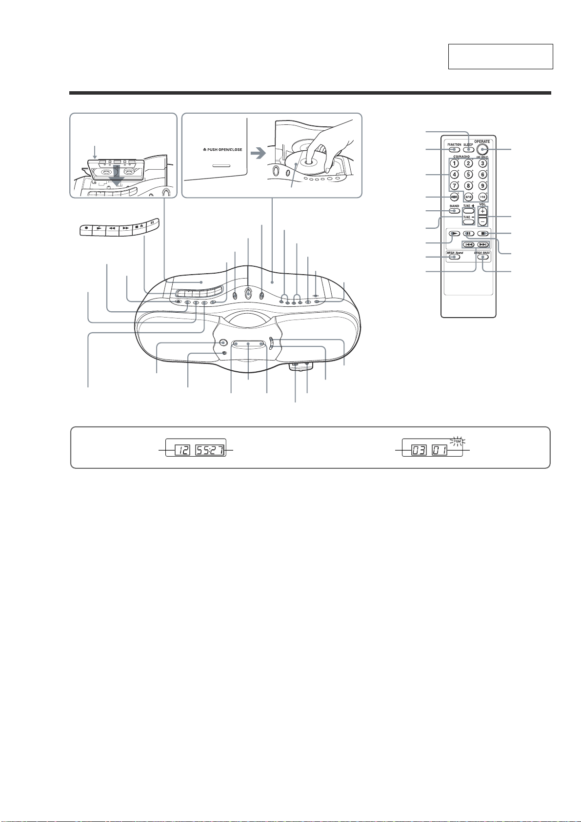
Location of controls
Inserting a cassette
With the side you want
to play facing upward
Loading a CD
SECTION 2
GENERAL
Remote Control
SLEEP
FUNCTION
Number buttons
CFD-F10/F10L
This section is extracted
from instruction manual.
OPERATE
(POWER)
*
LINE
(CFD-F10L only)
TAPE
RADIO BAND
AUTO PRESET
i
OPERATE
(POWER)
SLEEP
MEGA BASS
VOLUME +*, –
MEGA Xpand
CD
OPR/BATT
With the labeled side up
TUNE –, +
m,M
PRESET –, +
., >
Display
Remote Sensor
OPTICAL DIGITAL OUT (CD)
(CFD-F10L only)
u*
Z PUSH
OPEN/CLOSE
x
MODE
DSPL/ENT/ MEM
LINE IN (CFD-F10L only)
MODE
BAND
TUNE +, –
N
MEGA Xpand
.,>
*The button has a tactile dot.
Display
DE
Total track number
Total playing time
Programmed track Playing order
VOL +*, –
x
X
MEGA BASS
5
CFD-F10/F10L
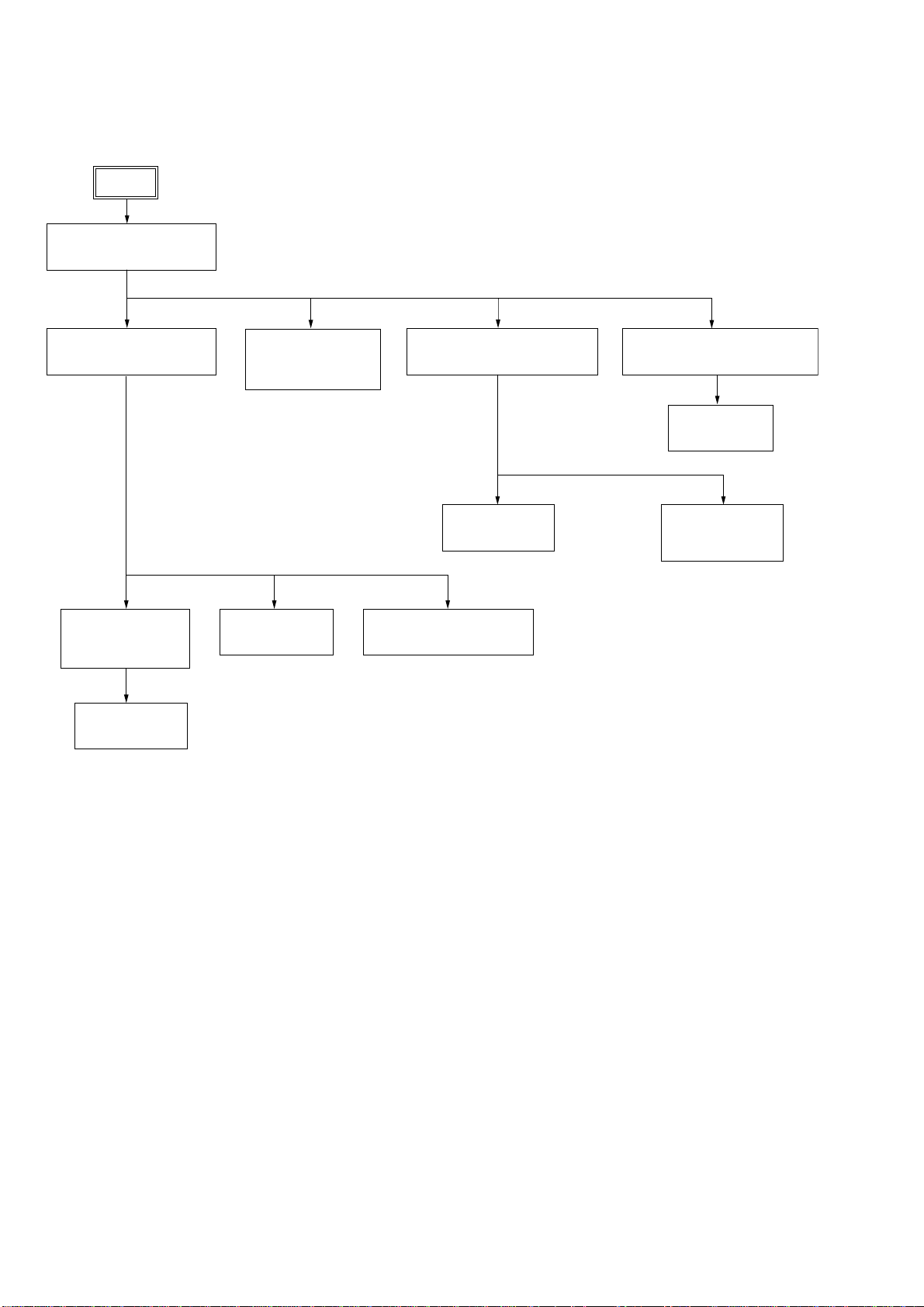
SECTION 3
DISASSEMBLY
• The equipment can be removed using the following procedure.
SET
3-1.CABINET UPPER ASSY
(Page 7)
3-3.CABINET REAR ASSY
(Page 8)
3-5.LED-1 BOARD,
LED-2 BOARD
(Page 9)
3-2.RELAY1 BOARD,
RELAY2 BOARD
(Page 8)
3-4.MAIN BOARD
(Page 9)
3-8.TAPE MECHANISM DECK
(Page 12)
3-9.TC BOARD
(Page 12)
3-7.LINE IN BOARD (F10L)
(Page 11)
3-11.CD MECHANISM SECTION
(Page 13)
3-12.CD BOARD
(Page 14)
3-10.MAIN BELT(B),
SUB BELT(B)
(Page 13)
3-6.LCD BOARD
(Page 10)
6
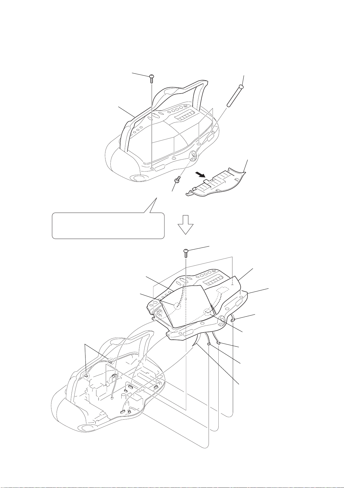
Note : Follow the disassembly procedure in the numerical order given.
4
four screws
(+BVTP)(B3)
5
three screws
(+BVTP)(B3)
6
two claws
2
screw
(+P)(M3)
1
battery lid
3
telescopic antenna
handle
7
wire (flat type)
(4 core) (CN407)
qa
wire (flat type)
(14 core) (CN803)
8
wire (flat type)
(13 core) (CN303)
9
connector
(4p) (CN302)
q;
connector
(7p) (CN304)
qs
connector
(3p) (CN314)
qd
cabinet upper assy
CD lid
CASSETTE lid
Caution
:
In order to remove the Cabinet upper assy,
the Telescopic antenna fixing screw that is located
inside the Battery lid should be removed.
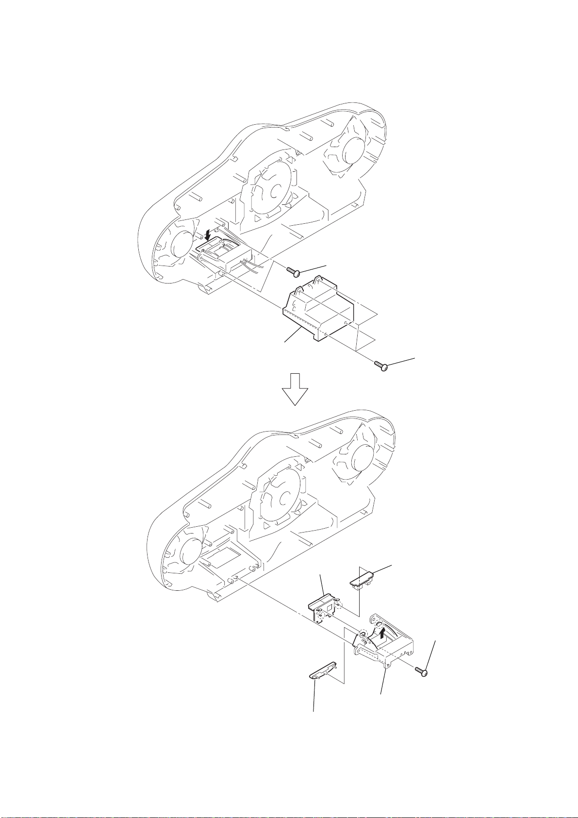
3-1. CABINET UPPER ASSY
CFD-F10/F10L
7
CFD-F10/F10L
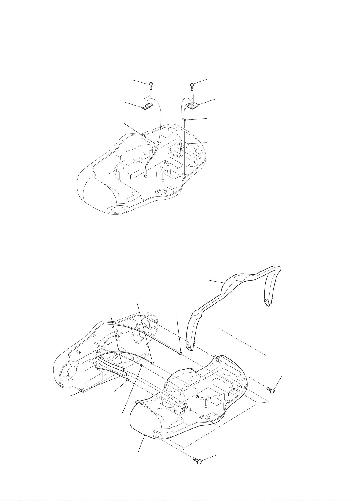
3-2. RELAY1 BOARD, RELAY2 BOARD
6
two screws
(+BVTP)(B2.6)
7
RELAY2 board
5
wire (flat type)
(4 core) (CN406)
1
two screws
(+BVTP)(B2.6)
4
RELAY1 board
2
connector
(5p) (CN308)
3
connector
(4p) (CN323)
3-3. CABINET REAR ASSY
2
wire (flat type)
(14 core) (CN806)
3
wire (flat type)
(12 core) (CN802)
7
connector
(3p) (CN313)
6
connector
(2p) (CN804)
5
connector
(3p) (CN312)
4
connector
(4p) (CN323)
1
handle
8
five screws
(+BVTP)(B3)
9
q;
cabinet rear assy
five screws
(+BVTP)(B3)
8
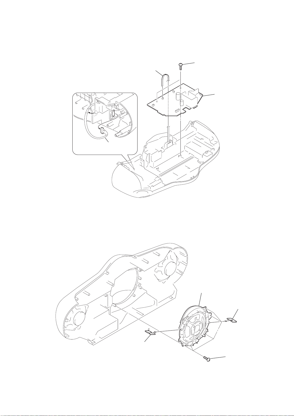
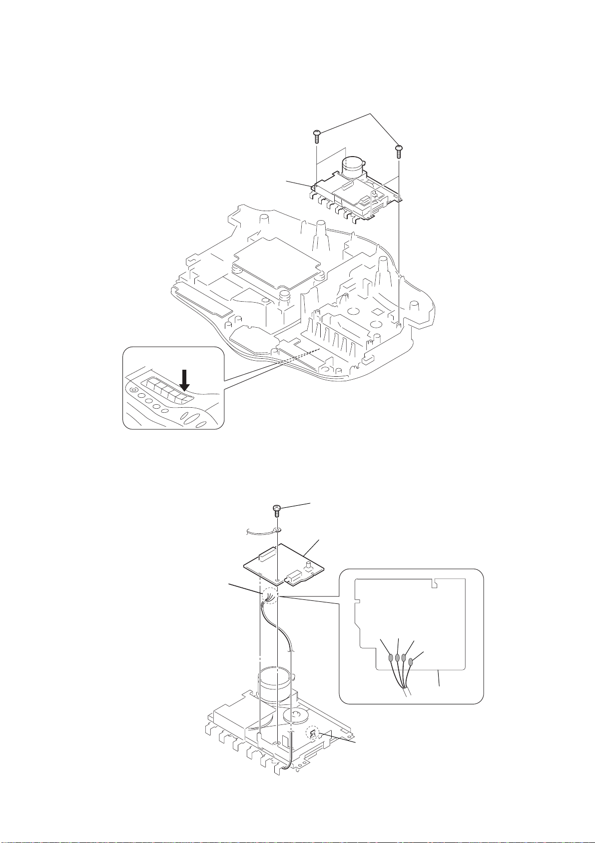
3-4. MAIN BOARD
d
)
2
connector
(11p) (CNP1)
1
wire (flat type)
(15 core) (CN320)
3
two screws
(+BVTP)(B2.6)
4
MAIN boar
CFD-F10/F10L
3-5. LED-1 BOARD, LED-2 BOARD
4
LED-2 board
2
back light chassis section
3
LED-1 board
1
six screws
(+BVTP)(B3
9
CFD-F10/F10L
3-6. LCD BOARD
6
power button
5
four screws
4
four screws
(+BVTP)(B2.6)
7
LCD board
3
cover rear
2
four screws
(+BVTP)(B2.6)
1
four screws
(+BVTP)(B2.6)
10
3-7. LINE IN BOARD (F10L)
)
3
4
two screws
(+BVTP)(B3)
CFD-F10/F10L
2
cover MD
9
cover MD link
1
four screws
(+BVTP)(B3
0
LINE IN board
5
7
screw
(+P)(B2.6)
8
door MD link
6
MD link section
11
CFD-F10/F10L
3-8. TAPE MECHANISM DECK
3
tape mechanism deck
1
four screws
(+BVTP)(B3)
3-9. TC BOARD
3
Remove soldering from the four points.
2
stop/eject knob
1
4
screw
TC board
yellow
red
gray
black
12
2
TC board
hook
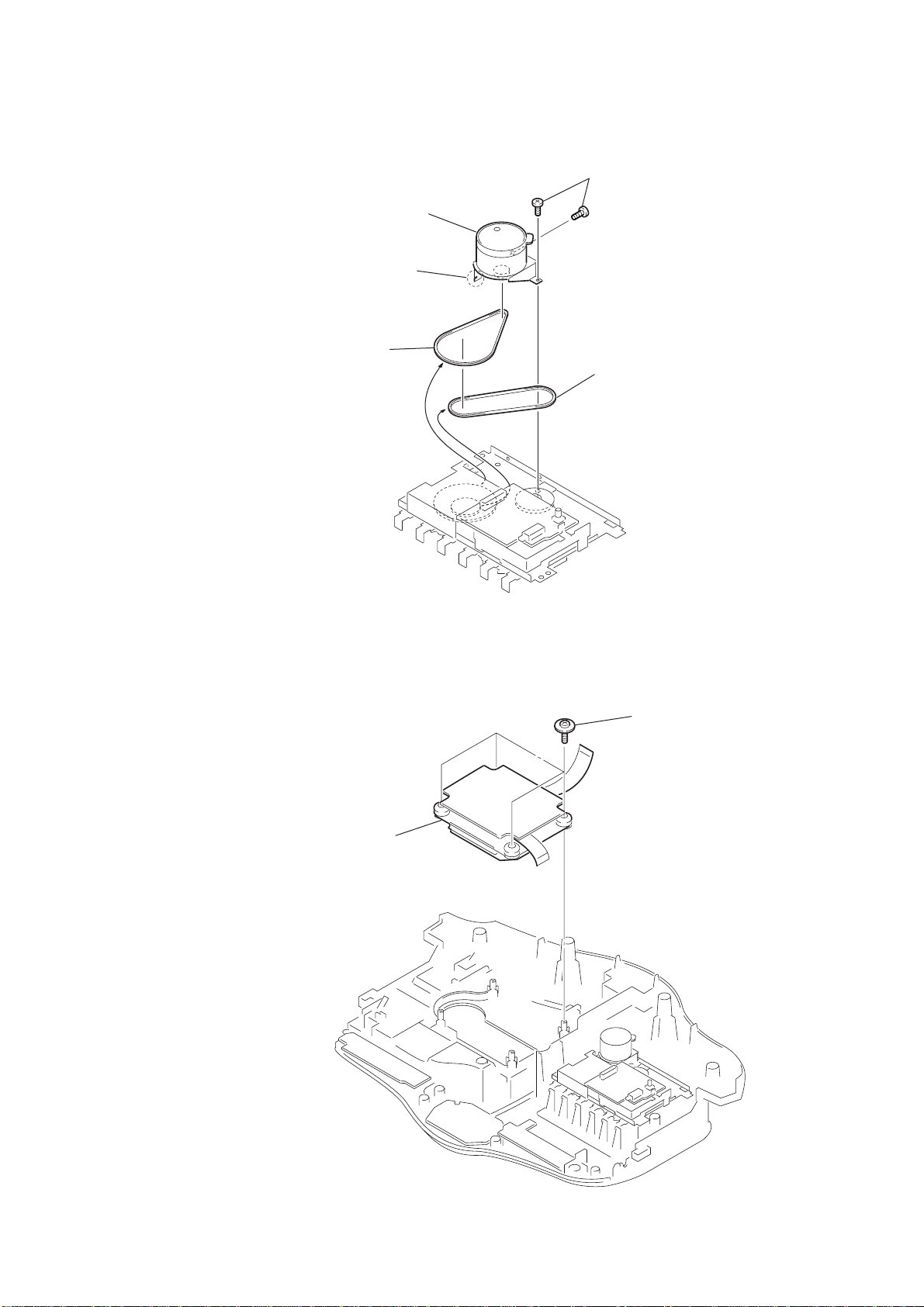
3-10. MAIN BELT (B), SUB BELT (B)
1
two screws
(+bind DT M2x 6)
3
pulley motor section
2
pulley motor section
4
main belt (B)
5
sub belt (B)
CFD-F10/F10L
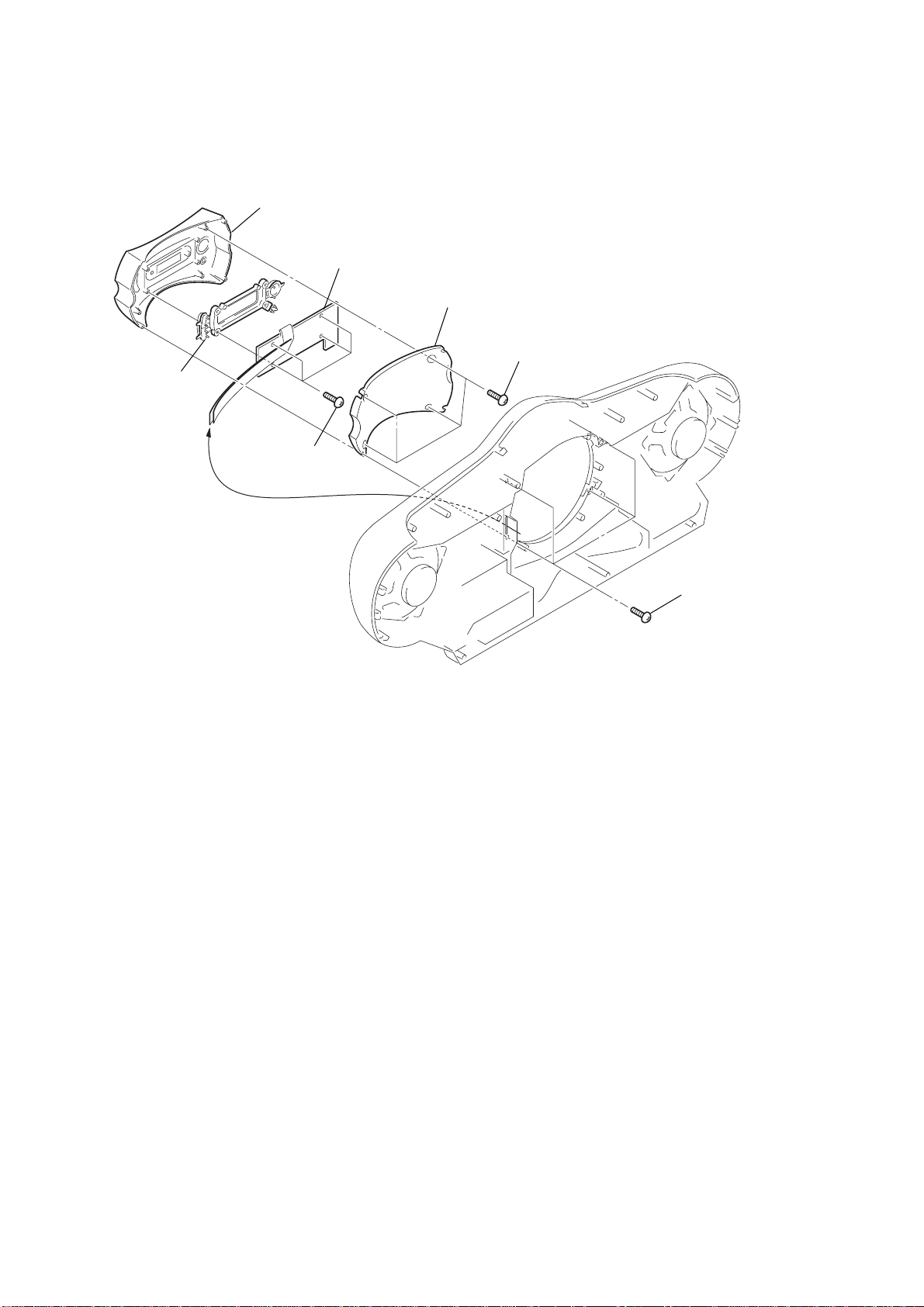
3-11. CD MECHANISM SECTION
2
CD mechanism section
1
four screws
(+PWH 2.6 x10)
13
CFD-F10/F10L
)
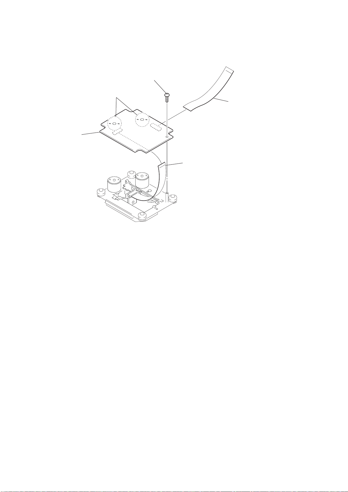
3-12. CD BOARD
2
Remove soldering from the four points.
5
CD board
1
screw
(+BVTP 2 × 6)
4
wire (flat type)
(16 core) (CNP701)
3
wire (flat type)
(14 core) (CNP702
14
SECTION 4
Tape speed adjustment
control inside motor
MECHANICAL ADJUSTMENTS
CFD-F10/F10L
SECTION 5
ELECTRICAL ADJUSTMENTS
PRECAUTION
1. Clean the following parts with a denatured-alcohol-moistened
swab :
record/playback head pinch roller
erase head rubber belts
capstan idlers
2. Demagnetize the record/playback head with a head demagnetizer. (Do not bring the head magnetizer close to the erase head.)
3. Do not use a magnetized screwdriver for the adjustments.
4. The adjustments should be performed with the rated power
supply voltage (9V) unless otherwise noted.
Torque Measurement
Mode Torque meter Meter reading
2.95 – 6.86 mN • m
FWD CQ-102C (30 – 70 g • cm)
(0.42 – 0.97 oz • inch)
FWD
Back T ension
FF CQ-201B (more than 60 g • cm)
REW CQ-201B (more than 60 g • cm)
CQ-102C (1.5 – 5.5 g • cm)
0.15 – 0.53 mN • m
(0.021 – 0.076 oz • inch)
more than 5.88 mN • m
(more than 0.83 oz • inch)
more than 5.88 mN • m
(more than 0.83 oz • inch)
TAPE SECTION 0 dB = 0.775 V
• Standard Output Level
Output terminal HP OUT
load impedance 32 Ω
output signal level 0.25 V (–10 dB)
• Test T ape
Type Signal Used for
WS-48A 3 kHz, 0 dB tape speed adjustment
Tape Speed Adjustment
Procedure:
Mode: playback
test tape
WS-48A
(3 kHz, 0 dB)
set
i
jack (J321)
Adjust so that the value on the digital frequency counter is
3,000 Hz.
digital frequency
counter
Ω
32
Tape Tension Measurement
Mode Tension meter Meter Reading
FWD CQ-403A
more than 100 g
(more than 3.53 oz)
Specification V alue:
Digital frequency counter
2,940 to 3,060 Hz
Adjust so that the frequency at the beginning and that at the end of
tape winding are between 2,970 to 3,030 Hz.
Adjustment Location:
15
CFD-F10/F10L
)
TUNER SECTION 0 dB = 1 µV
• AM Section
Setting:
RADIO BAND•AUTO PRESET button: MW or LW
AM RF signal
generator
30% amplitude
modulation by
400 Hz signal
• FM Section
Setting:
RADIO BAND•AUTO PRESET button: FM
FM RF signal
generator
75 kHz frequency
deviation by 1 kHz signal
output level : as low as possible
• Connecting Level Meter (FM, MW and LW)
set
Put the lead-wire
antenna close to
the set.
0.01
µ
F
level meter
(range: 0.5–5 V ac
Ω
32
TP (FM IN)
set
MW IF ADJUSTMENT
Adjust for a maximum reading on level meter.
T1
450 kHz
MW FREQUENCY COVERAGE
CHECK
Frequency Display 531 kHz 1,611 kHz
Reading on Digital voltmeter 1.0 ± 0.5 V 5.2 ± 0.6 V
Adjustment Part <confirmation> <confirmation>
MW TRACKING ADJUSTMENT
Adjust for a maximum reading on level meter.
L3-1 CT3
621 kHz 1,404 kHz
LW FREQUENCY COVERAGE
ADJUSTMENT
Frequency Display 153 kHz 279 kHz
Reading on Digital voltmeter 0.6 ± 0.3 V 5.0 ± 0.1 V
Adjustment Part <confirmation> L4
LW TRACKING ADJUSTMENT
Adjust for a maximum reading on level meter.
L3-2 CT5
162 kHz 261 kHz
FM IF ADJUSTMENT
Adjust for a maximum reading on level meter.
T2
10.7 MHz
i
jack (J321)
• Connecting Digital Voltmeter (FM, MW and LW)
digital
voltmeter
Ω
100 k
TP (VT)
•Repeat the procedures in each adjustment several times, and the
frequency coverage and tracking adjustments should be finally
done by the trimmer capacitors.
FM FREQUENCY COVERAGE
ADJUSTMENT
Frequency Display 87.5 MHz 108 MHz
Reading on Digital voltmeter 1.3 ± 0.3 V 3.0 ± 0.2 V
Adjustment Part <confirmation> L2
FM TRACKING ADJUSTMENT
Adjust for a maximum reading on level meter.
L1 CT1
87.5 MHz 108 MHz
Adjustment Location: See page 17.
16
Adjustment Location:
– MAIN board (component side) –
CFD-F10/F10L
CT5, L3-2
LW
TRACKING
ADJUSTMENT
L3-2 L3-1
CT1, L1
FM
TRACKING
ADJUSTMENT
L2
L2
FM
FREQUENCY
COVERAGE
ADJUSTMENT
TP (FM IN)
(CONDUCTOR SIDE)
T1
MW
IF
ADJUSTMENT
T2
FM
IF
ADJUSTMENT
T1
T2
L1
CT1
IC1
CD SECTION
CD section adjustments are done automatically in this set.
In case of operation check, confirm that focus bias.
CT3
L4
CT5
L4
LW
FREQUENCY
COVERAGE
ADJUSTMENT
TP (VT)
(CONDUCTOR SIDE)
CT3, L3-1
MW
TRACKING
ADJUSTMENT
IC2
FOCUS BIAS CHECK
1. Connect the oscilloscope between IC701 pin 4 and pin qa (or
TP (RF) and TP (VREF)).
2. Insert the disc (YEDS-18). (Part No. : 3-702-101-01)
3. Press the NX (CD) button.
4. Confirm that the oscilloscope waveform is as shown in the
figure below. (eye pattern)
A good eye pattern means that the diamond shape ( ) in the
center of the waveform can be clearly distinguished.
• RF signal reference waveform (eye pattern)
VOLT/DIV : 50 mV (10 : 1 probe in use)
TIME/DIV : 500 nS
RF level :
0.85
±
0.2 Vp-p
When observing the eye pattern, set the oscilloscope for AC range
and raise vertical sensitivity.
Test Point:
– CD board (conductor side) –
R734
R736
R706
R701
C739
C707
C732
TP
(VREF)
JW709
R710
R733
R735
JW708
JW706
R709
C736
JC703
R711
C705
C708
R713
C734
JW707
TP
(RF)
C742
R723
C704
R708
JW726
C731
C743
JW725
C703
C709
R729
IC701
C711
17
CFD-F10/F10L
d
CIRCUIT BOARD LOCATION
SECTION 6
DIAGRAMS
H/P board
POWER board
CONT1 board
TC board
LCD board
RELAY1 board
CONT3 board
BATT-2 board
RELAY2 board
CD board
TUNER boar
MAIN board
CONT2 board
LED-1 board
BATT-1 board
LED-2 board
LINE IN board
(F10L)
18
 Loading...