

Page 1
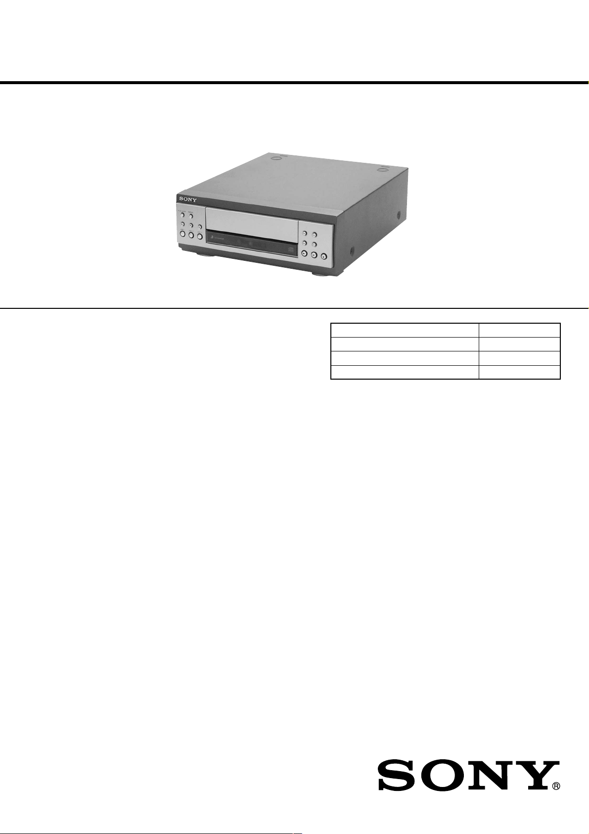
CDP-S3
SERVICE MANUAL
Ver 1.0 2001.04
CDP-S3 is the CD player section
in MHC-S7AV or MHC-S3.
AEP Model
UK Model
E Model
Australian Model
Model Name Using Similar Mechanism NEW
CD Mechanism Type CDM63B-30BD60
Base Unit Name BU-30BD60
Optical Pick-up Name OP Assy (A-MAX.3)
SPECIFICATIONS
System Compact disc and digital
Laser Semiconductor laser
Frequency response 2 Hz – 20 kHz (±0.5 dB)
Signal-to-noise ratio More than 90 dB
Dynamic range More than 90 dB
OPTICAL OUT
(Square optical connector jack, rear panel)
Dimensions (w/h/d)
Mass Approx. 2.7 kg
Design and specifications are subject to change
without notice.
audio system
(λ=780 nm)
Emission duration:
continuous
Approx. 280 x 108 x 330 mm
9-873-831-11 Sony Corporation
2001D0500-1 Home Audio Company
C 2001.4 Shinagawa Tec Service Manual Production Group
COMPACT DISC PLAYER
Page 2
CDP-S3
NOTES ON HANDLING THE OPTICAL PICK-UP
BLOCK OR BASE UNIT
The laser diode in the optical pick-up block may suffer electrostatic break-down because of the potential difference generated
by the charged electrostatic load, etc. on clothing and the human
body.
During repair, pay attention to electrostatic break-down and also
use the procedure in the printed matter which is included in the
repair parts.
The flexible board is easily damaged and should be handled with
care.
NOTES ON LASER DIODE EMISSION CHECK
The laser beam on this model is concentrated so as to be focused
on the disc reflective surface by the objective lens in the optical
pick-up block. Therefore, when checking the laser diode emission, observe from more than 30 cm away from the objectiv e lens.
LASER DIODE AND FOCUS SEARCH OPERATION
CHECK
Carry out the “S curve check” in “CD section adjustment” and
check that the S curve waveforms is output three times.
Notes on chip component replacement
• Never reuse a disconnected chip component.
• Notice that the minus side of a tantalum capacitor may be dam-
aged by heat.
CAUTION
Use of controls or adjustments or performance of procedures
other than those specified herein may result in hazardous radiation exposure.
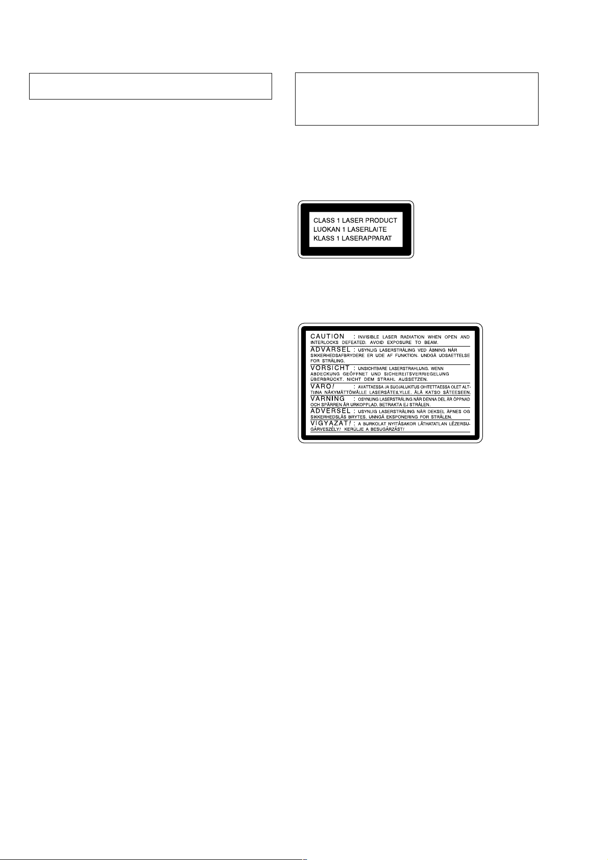
This appliance is classified as a CLASS 1 LASER product.
The CLASS 1 LASER PRODUCT MARKING is located on
the rear exterior.
Laser component in this product is capable of emitting radiation
exceeding the limit for Class 1.
The following caution label is located inside the unit.
Flexible Circuit Board Repairing
• Keep the temperature of the soldering iron around 270 ˚C during repairing.
• Do not touch the soldering iron on the same conductor of the
circuit board. (within 3 times)
• Be careful not to apply force on the conductor when soldering
or unsoldering.
SAFETY-RELATED COMPONENT WARNING!!
COMPONENTS IDENTIFIED BY MARK 0 OR DOTTED
LINE WITH MARK 0 ON THE SCHEMATIC DIAGRAMS
AND IN THE PARTS LIST ARE CRITICAL TO SAFE
OPERATION. REPLACE THESE COMPONENTS WITH
SONY PARTS WHOSE PART NUMBERS APPEAR AS
SHOWN IN THIS MANUAL OR IN SUPPLEMENTS PUBLISHED BY SONY.
2
Page 3

TABLE OF CONTENTS
1. SERVICING NOTES............................................... 4
2. GENERAL ................................................................... 5
3. DISASSEMBLY
3-1. Disassembly Flow ........................................................... 6
3-2. Cover ............................................................................... 7
3-3. CD Mechanism Deck (CDM63B-30BD60) ................... 7
3-4. MAIN Board ................................................................... 8
3-5. Front Panel Section ......................................................... 8
3-6. PANEL (L) Board, PANEL (R) Board ........................... 9
3-7. Lid (CD) .......................................................................... 9
4. TEST MODE.............................................................. 10
5. ELECTRICAL ADJUSTMENTS......................... 11
6. DIAGRAMS
6-1. Note for Printed Wiring Boards
and Schematic Diagrams ................................................ 12
6-2. Printed Wiring Board – BD Section – ........................... 14
6-3. Schematic Diagram –BD Section – ............................... 15
6-4. Printed Wiring Boards – CD CHANGER Section – ..... 16
6-5. Schematic Diagram – CD CHANGER Section – ......... 17
6-6. Printed Wiring Board – MAIN Section – ...................... 18
6-7. Schematic Diagram – MAIN Section –......................... 19
6-8. Printed Wiring Boards – PANEL Section – .................. 20
6-9. Schematic Diagram – PANEL Section – ....................... 21
6-10. IC Pin Function Description ........................................... 24
CDP-S3
7. EXPLODED VIEWS
7-1. General Section ............................................................... 26
7-2. CD Mechanism Deck Section-1
(CDM63B-30BD60) ....................................................... 27
7-3. CD Mechanism Deck Section-2
(CDM63B-30BD60) ....................................................... 28
7-4. Base Unit Section (BU-30BD60) ................................... 29
8. ELECTRICAL PARTS LIST ............................... 30
3
Page 4
CDP-S3
SECTION 1
SERVICING NOTES
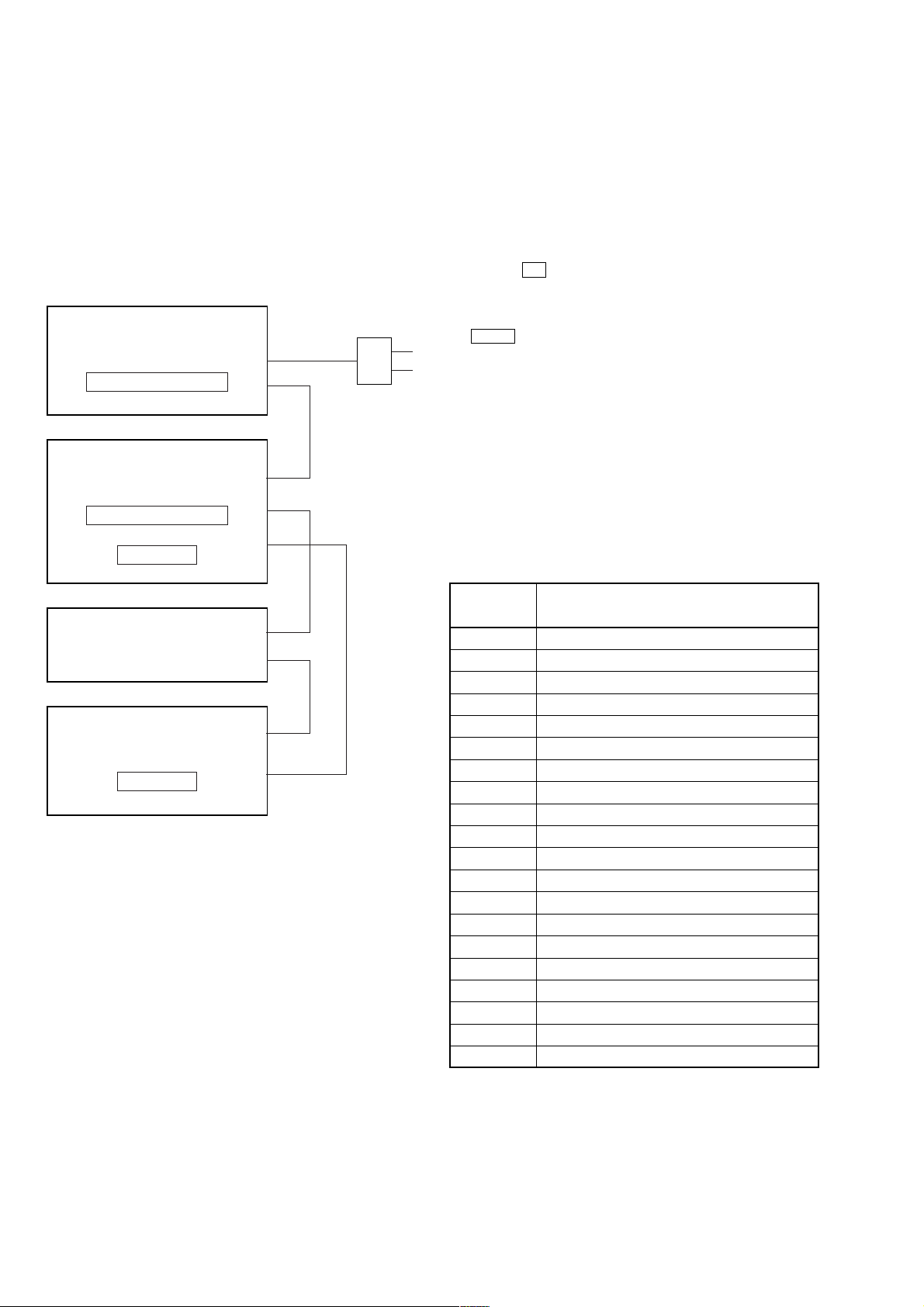
This set is a component of the MHC-S7AV or MHC-S3.
The MHC-S7AV or MHC-S3 system configuration is as shown
below, and therefore it does not operate normally unless all four
components are connected.
In performing the repair, connect all components with the system
cables.
Note: The precaution to the users is described on the label stuck on
the back panel (CD player) and in the troubleshooting section in
the Operation Manual.
System Configuration:
AC IN
TA
POWER SUPPLY
ST
SYSTEM & CD µcon
DISPLAY
CDP
TC
TC µcon
CD-TEXT TEST DISC
This unit is able to display the test data (character information)
written in the CD on its fluorescent indicator tube.
The CD-TEXT TEST DISC (TGCS-313:4-989-366-01) is used
for checking the display.
To check, perform the following procedure.
Checking Method:
1. Press the I/1 button to turn the power on, set the disc to the
disc table with the “test disc” label facing up, and chuck the
disc.
2. Press the [CD] button to set CD function, and press the
n N button to playback the disc.
3. The following will be displayed on the liquid crystal display.
Display : 1KHZ/0DB/L R
4. Pressing the [-- ] or [ +] button, select the track. The te xt
data of each track will be displayed.
For details of the displayed contents for each track, refer to “Table
1 : CD-TEXT TEST DISC TEXT Data Contents”.
Restrictions in CD-TEXT Display
In this unit, some special characters will not be displayed properly. These will be displayed as a space or a character resembling
it.
Table 1 : CD-TEXT TEST DISC TEXT Data Contents
(TRACKS No. 1 to 20:Normal Characters)
TRACK
No.
1 1kHz/0dB/L&R
2 20Hz/0dB/L&R
3 40Hz/0dB/L&R
4 100Hz/0dB/L&R
5 200Hz/0dB/L&R
6 500Hz/0dB/L&R
7 1kHz/0dB/L&R
8 5kHz/0dB/L&R
9 7kHz/0dB/L&R
10 10kHz/0dB/L&R
11 16kHz/0dB/L&R
12 18kHz/0dB/L&R
13 20kHz/0dB/L&R
14 1kHz/0dB/L&R
15 1kHz/–1dB/L&R
16 1kHz/–3dB/L&R
17 1kHz/–6dB/L&R
18 1kHz/–10dB/L&R
19 1kHz/–20dB/L&R
20 1kHz/–60dB/L&R
Note: Track No. 21 to 99 are not displayed.
.>
Displayed Contents
4
Page 5
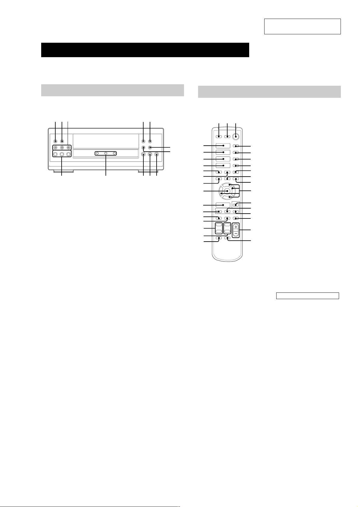
Parts Identification
x
hH
H
hH
O
o
Pp
Mm
X
>
.
123
wg
qh
qa
wk
wj
wh
wa
4
5
6
7
qs
qf
qd
qg
8
9
q;
qk
ql
w;
qj
wd
ws
wf
es
ea
e;
wl
CD H es (14, 15)
CHECK 5 (15)
CLEAR 6 (15)
CLOCK/TIMER SELECT qj
(30)
CLOCK/TIMER SET qk (13, 21,
29)
DBFB qg (23)
DISPLAY ws (13, 16, 18, 29, 35)
D.SKIP 4 (14)
ENTER wg (10, 12, 13, 15, 17,
18, 21, 22, 26–30)
EQ qd (27)
EQ ON/OFF qf (10, 28)
FUNCTION wf (10, 14, 15, 20,
21, 31)
GROOVE wa (23)
SET UP qs (10, 12, 26, 28, 29)
SLEEP 7 (29)
SUR wd (25)
TAPE A hH ea (19, 35)
TAPE B hH e; (19, 20, 35)
TUNER/BAND wl (17)
TUNING + 9 (17)
TUNING – wh (17)
TV CH +/– ql
TV VOL +/– w;
TV @/1 2
TV/VIDEO 1
VOL +/– qh
BUTTON DESCRIPTIONS
@/1 (power) 3
X (pause) q;
x (stop) 8
. (go back) wk
> (go forward) wj
m (rewind) wh
M (fast forward) 9
O/o/P/p qa
Remote Control
The items are arranged in alphabetical order.
Refer to the pages indicated in parentheses ( ) for details.
Main unit
SECTION 2
GENERAL
CDP-S3
This section is extracted from
instruction manual.
wj wkwl e;
1 2 3
ek
DISC 1–3 ek (14, 15, 21)
DISC 1–3 indicators ej
DISC 1–3 Z (eject) wl (14)
PLAY MODE wj (14, 15, 21)
REPEAT wk (14)
N (play) eh (14, 15)
X (pause) eg (14)
x (stop) ef (14, 20)
. (go back) ed (14, 15, 21)
> (go forward) es (14, 15, 21)
m (rewind) e; (14)
M (fast forward) ea (14)
ea
mM
>
.
HS x
efegehej
es
ed
5
Page 6
CDP-S3
• This set can be disassembled in the order shown below.
3-1. DISASSEMBLY FLOW
SET
3-2. COVER
(Page 7)
SECTION 3
DISASSEMBLY
3-3. CD MECHANISM DECK
(CDM63B-30BD60)
(Page 7)
3-4. MAIN BOARD
(Page 8)
3-5. FRONT PANEL SECTION
(Page 8)
3-6. PANEL (L) BOARD,
PANEL (R) BOARD
(Page 9)
3-7. LID (CD)
(Page 9)
6
Page 7
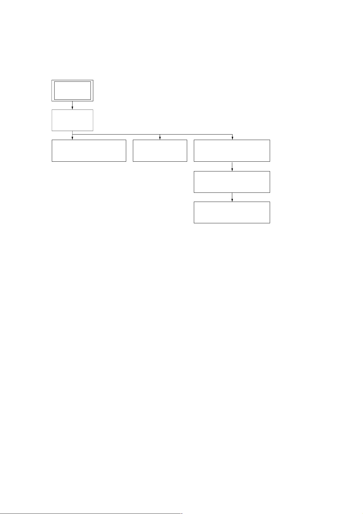
Note: Follow the disassembly procedure in the numerical order given.
)
r
3-2. COVER
3
cover
1
two screws
(case 3 TP2)
2
screw
(BVTT3 × 6)
CDP-S3
3-3. CD MECHANISM DECK (CDM63B-30BD60)
4
CD mechanism deck (CDM63B-30BD60)
1
two screws
(case 3 TP2
2
connecto
(CN701)
3
four screws
(BVTP3
1
wire (flat type) (21 core)
(CN301)
×
8)
7
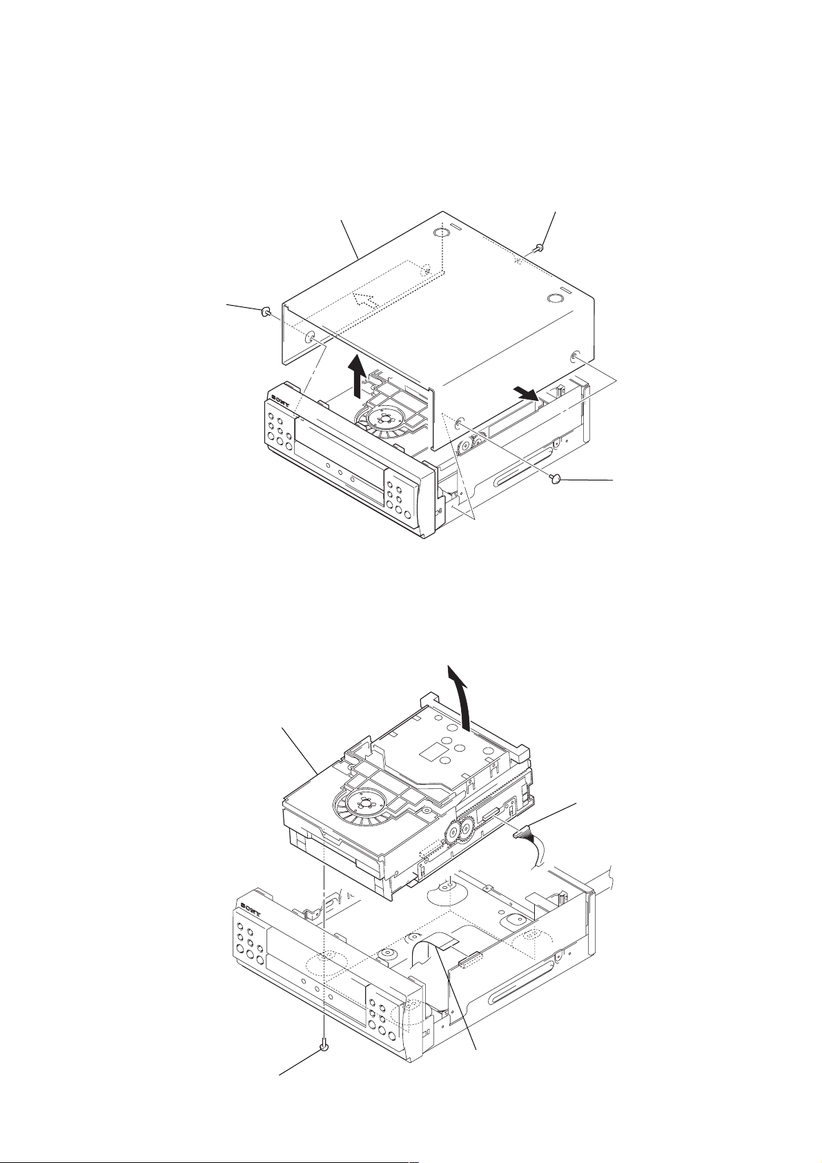
Page 8
CDP-S3
)
3-4. MAIN BOARD
1
wire (flat type) (21 core)
(CN301)
2
connector
(CN401)
2
two connectors
(CN101, 102)
5
3
screw
(BVTP3 × 8)
MAIN board
3
two screws
(BVTP3 × 8
3-5. FRONT PANEL SECTION
3
4
front panel section
claw
2
connector
(CN701)
3
1
connector
(CN401)
4
lug
screw
(BVTP3 × 8)
3
two claws
2
three screws
(BVTP3
×
8)
8
Page 9
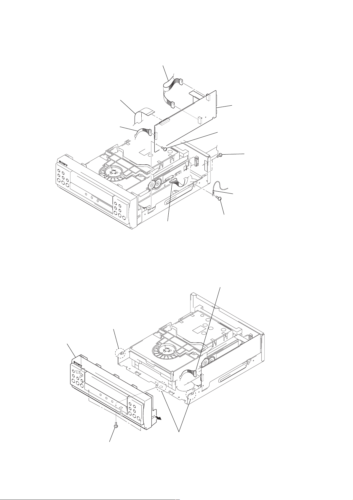
3-6. PANEL (L) BOARD, PANEL (R) BOARD
d
)
4
6
PANEL (R) board
5
two claws
four screws
(BVTP2.6
CDP-S3
×
8)
1
five screws
(BVTP2.6
3
×
8)
PANEL (L) boar
3-7. LID (CD)
4
spring (CD)
2
two claws
2
bracket (LID) assy
1
screw
(BVTP2.6 × 8
3
lid (CD)
9
Page 10

CDP-S3
SECTION 4
TEST MODE
Note: Use flowing buttons in the test mode.
no mark: Button of CD unit (CDP-S3)
*1 : Button of amplifier unit (TA-S7AV or TA-S3)
*2 : Button of tuner unit (ST-S5 or ST-S3)
[CD Delivery Mode]
• This mode moves the optical pick-up to the position durable to
vibration. Use this mode when returning the set to the customer
after repair.
Procedure:
1. Press the I/1 *1 button to turn the power on.
2. Turn the [FILE SELECT] *1 knob to set the CD function.
3. While pressing the [EQ ON/OFF] *1 button, press the I/1 *
button.
4. The message “LOCK” is displayed on the fluorescent indica-
tor tube of tuner unit and turn the power off automatically , and
the CD delivery mode is set.
[GC Test Mode]
Enter the GC Test Mode
Procedure 1:
1. Press the I/1 *1 button to turn the power on.
2. While pressing the both [PLAY MODE] and [ ] b uttons, press
Z
the [ ] (DISC 1) button.
x
3. LEDs and fluorescent indicator tube are all turned on of all
units.
Procedure 2:
1. Press the I/1 *1 button to turn the power on.
2. While pressing the both [STEREO/MONO] *2 and
[CINEMA STUDIO C] *
1
buttons, press the [CLOCK/TIMER]
*2 button.
3. LEDs and fluorescent indicator tube are all turned on of all
units.
[CD Service Mode]
• This mode can run the CD sled motor optionally. Use this mode,
for instance, when cleaning the optical pick-up.
Procedure:
1. Press the I/1 *1 button to turn the power on.
2. Turn the [FILE SELECT] *1 knob to set the CD function.
3. While pressing the both [PLAY MODE] and [ ] b uttons, press
.
the [ ] button.
x
4. Set to the CD service mode.
5. With the CD in stop status, press the [ ] button to move the
M
optical pick-up to outside track, or press the [ ] button to
1
inside track.
6. To release from this mode, perform as follows.
1) Move the optical pick-up to the most inside track.
2) Disconnect the power cord.
Notes: • Always move the optical pick-up to most inside track when
releasing from this mode. Otherwise, a disc will not be unloaded.
• Do not run the sled motor excessively, otherwise the gear can
be chipped.
[CD Cancellation Mode of Repeat Limitation]
• This mode can cancel the CD repeat limitation (5 times).
Procedure:
1. Press the I/1 *1 button to turn the power on.
2. Turn the [FILE SELECT] *1 knob to set the CD function.
3. While pressing the both [PLAY MODE] and [ ] b uttons, press
x
the [REPEAT] button.
4. CD repeat limitation is canceled.
5. To release this mode, disconnect the power cord.
m
Version Display Mode
Procedure:
1. Enter the GC test mode.
2. Each time the
[DISC 1] or [TUNER MEMORY] *
2
button is
pressed, microcomputer or mechanism deck version is displayed of each unit.
3. Press the [DISC 3] or [TUNING +] *2 button to detail is displayed the version.
Key Check Mode
Procedure:
1. Enter the GC test mode.
2. Press the [DISC 2] or [TUNING --] *2 button to set the key
check mode, and displays “K 0 J 0 V 0” on the fluorescent
indicator tube of tuner unit.
3. All buttons are pressed of CD unit, all LEDs are blinking of
CD unit. (not change the display of fluorescent indicator tube)
Releasing the GC Test Mode
T o release from this mode, press three buttons in the same manner
as entering this mode or disconnect the power cord.
10
Page 11
SECTION 5
p
e
)
ELECTRICAL ADJUSTMENTS
CDP-S3
Note :
1. CD Block is basically designed to operate without adjustment.
Therefore, check each item in order given.
2. Use LUV-P01 (4-999-032-01) unless otherwise indicated.
3. Use an oscilloscope with more than 10MΩ impedance.
4. Clean the object lens by an applicator with neutral detergent
when the signal level is low than specified value with the
following checks.
S-Curve Check
Oscilloscope
BD board
TP(FEO)
TP(DVC)
Procedure :
1. Connect an oscilloscope to TP (FEO).
2. Connect between TP (FEI) and TP (DVC) ( 1.65 V) by lead
wire.
3. Turn Power switch on.
4. Load a disc (LUV-P01) and actuate the focus search. (In
consequence of open and close the disc tray, actuate the focus
search)
5. Confirm that the oscilloscope waveform (S-curve) is
symmetrical between A and B. And confirm peak to peak level
within 2 ± 0.5 Vp-p.
S-curve waveform
symmetry
E-F Balance (1 Track jump) Check
oscilloscop
BD board
TP(TEO)
TP(DVC)
Procedure :
1. Connect an oscilloscope to TP (TEO) and TP (DVC).
2. Turn Power switch on.
3. Load a disc (LUV -P01) and playback the number nine track.
4. Press the N button. (Becomes the 1 track jump mode.)
5. Confirm that the level B and A (DC voltage) on the oscilloscope
waveform.
1 track jump waveform
DVC
level=1.0 ±0.5Vp-p
B
symmetry
center of
waveform
A (DC voltage
6. Adjust RV101 on the BD board so that the center of wa veform
becomes the same voltage of DVC. (i.e. A=0V)
Adjustment Location:
A
±
within 2
B
0.5Vp-
6. After check, remove the lead wire connected in step 2.
Note : • Try to measure several times to make sure than the ratio
of A : B or B : A is more than 10 : 7.
• Take sweep time as long as possible and light up the
brightness to obtain best waveform.
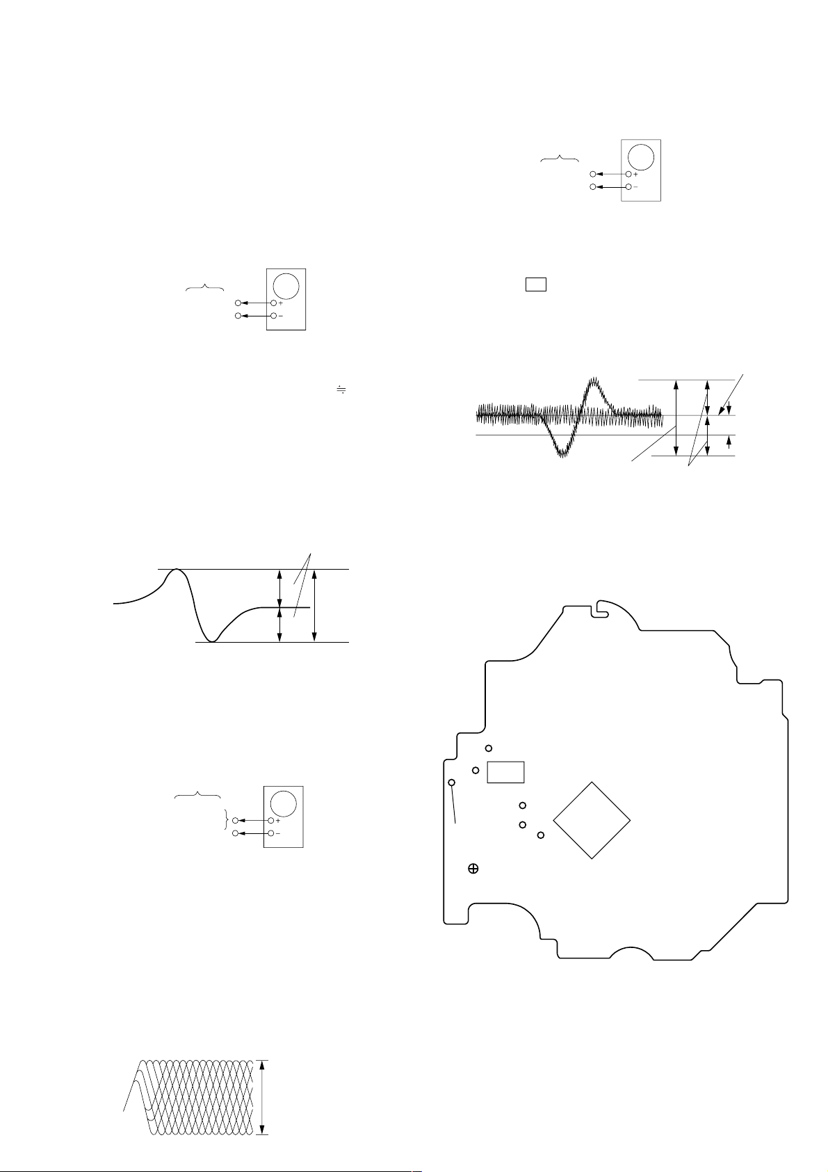
RF Level Check
BD board
TP(RFDC)
TP(RFAC)
TP(DVC)
oscilloscope
Procedure :
1. Connect an oscilloscope CH1 to TP (RFDC) and CH2 to TP
(RFAC).
2. Turn Power switch on.
3. Load a disc (LUV-P01) and playback.
4. Confirm that oscilloscope waveform is clear and check if RF
signal level is correct or not.
Note : Clear RF signal waveform means that the shape “ ◊ ” can be clearly
distinguished at the center of the waveform.
RF signal waveform
VOLT/DIV : 200mV
TIME/DIV : 500ns
[BD BOARD] (Conductor Side)
TP (DVC)
TP
15
IC103
16
1
30
TP
(RFDC)
40
41
IC101
60
(RFAC)
TP
(FEI)
RV101
TP (FEO)
TP (TEO)
2021
1
80
61
±
level : 0.65
0.15Vp-p (RFDC)
1.1
±
0.4Vp-p (RFAC)
11
Page 12

CDP-S3
B
These are omitted.
CE
Q
SECTION 6
DIAGRAMS
6-1. NOTE FOR PRINTED WIRING BOARDS AND SCHEMATIC DIAGRAMS
(In addition to this, the necessary note is printed in each block)
Note on Printed Wiring Boards:
• X : parts extracted from the component side.
• Y : parts extracted from the conductor side.
f
•
•
• Indication of transistor.
: internal component.
: Pattern from the side which enables seeing.
C
Q
B
E
These are omitted.
Note on Schematic Diagram:
• All capacitors are in µF unless otherwise noted. pF: µµF
50 WV or less are not indicated except for electrolytics
and tantalums.
• All resistors are in Ω and 1/
specified.
f
•
• C : panel designation.
Note: The components identified by mark 0 or dotted line
• A : B+ Line.
• Voltages are taken with a V OM (Input impedance 10 MΩ).
• Waveforms are taken with a oscilloscope.
• Circled numbers refer to waveforms.
• Signal path.
: internal component.
with mark 0 are critical for safety.
Replace only with part number specified.
Voltage variations may be noted due to normal production tolerances.
Voltage variations may be noted due to normal production tolerances.
J : CD PLAY
4
W or less unless otherwise
12
Page 13

• Circuit Boards Location
d
PANEL (R) board
CDP-S3
MAIN board
IN OUT SW board
BD board
DISC SENSOR board
PANEL (L) board
TRAY SENSOR board
DRIVER boar
MOTOR board
13
Page 14

CDP-S3
6-2. PRINTED WIRING BOARD – BD Section – • See page 13 for Circuit Boards Location.
(Page 18)
MAIN
BOARD
A
CN301
M102
(SLED)
M101
(SPINDLE)
• Semiconductor
Location
Ref. No. Location
D101 B-3
IC101 C-3
IC102 B-2
IC103 D-2
TP
(DVC)
TP
(RFDC)
TP
(FEO)
TP (TEO)
TP
(RFAC)
TP
(FEI)
Q101 C-1
Q102 A-3
14
There are a few cases that the part printed on
this diagram isn’t mounted in this model.
Page 15

6-3. SCHEMATIC DIAGRAM – BD Section –• See page 22 for Waveforms. • See page 22 for IC Block Diagrams.
TP (DVC)
TP
(RFDC)
TP (FEI)
TP
(RFAC)
CDP-S3
IC B/D
TP
(TEO)
TP
(FEO)
IC B/D
IC B/D
A
MAIN
BOARD
CN301
(Page 19)
Note: The components identified by mark 0 or dotted line
with mark 0 are critical for safety.
Replace only with part number specified.
• Voltages and waveforms are dc with respect to ground
under no-signal conditions.
no mark : CD PLAY
1515
Page 16

CDP-S3
6-4. PRINTED WIRING BOARDS – CD CHANGER Section –• See page 13 for Circuit Boards Location.
1
5
There are a few cases that the part isn't mounted in model
is printed on diagrams.
MAIN
BOARD
NO202
(Page 18)
1616
Page 17

6-5. SCHEMATIC DIAGRAM – CD CHANGER Section –• See page 22 for IC Block Diagram.
IC731
SUB TRAY1
HEIGHT SENSOR
CDP-S3
IC732
SUB TRAY2
HEIGHT SENSOR
IC733
SUB TRAY3
HEIGHT SENSOR
B
MAIN
BOARD
NO202
(Page 19)
IC751
DISC IN
DETECT
• Voltages and waveforms are dc with respect to ground
under no-signal conditions.
no mark : CD STOP
1717
Page 18

CDP-S3
6-6. PRINTED WIRING BOARD – MAIN Section –• See page 13 for Circuit Boards Location.
1 2 3 4 5 6 7 8 9 10
(Page 14)
BD BOARD
A
CN101
(Page 16)
DRIVER BOARD
B
CN701
SYSTEM CONTROL 3
TO ST-S3/S5
MAIN BOARD
A
B
C
D
C319
C318
CN401
C317
L310
R440
JW135
9
1
C316
C315
R437
C321
C314
C313
JW158
R465
R469
R473
R477
R481
CD313
C320
CD312
JW162
JW155
JW156
JW157
JW165
R433
JW164
R441
R442
JW150
C311
CD311
FB313
JW170
R443
R435
JW149
R452
FB312
R457
R447
CN301
C310
CD304
JW153
FB410
R446
R456
FB311
JW151
R450
C306
R449
R445
R444
R448
FB310
JW154
JW145
R453
JW144
R451
JW177
C304
C301
R438
JW176
C303
R460
R500
FB305
R436
C302
R459
JW175
R432
JW143
R430
C463
JW142
JW141
JW139
JW148
JW147
JW146
CD303
R429
R428
IC401
CD302
CD301
R426
R424
C462
R480
JW137
JW138
R419
R492
X401
R417
R495
1
1
IC402
R413
R497
FB314
FB315
C416
C499
14
8
JW120
R409
R403
C498
JW136
C425
JW171
R401
R496
112
NO202
JW122
R133
JW132
JW123
JW121
JW98
R489
R132
JW130
C261
C260
JW129
FB416
JW163
JW131
JW128
JW99
JW119
JW118
JW117
JW116
JW127
JW124
JW112
JW126
R402
C411
R411
R425
R483
C427
C401
R482
R134
R494
R427
JW169
JW178
C251
JW168
R493
JW172
C255
JW161
JW134
JW133
R412
R491
R490
JW167
JW125
D512
JW111
JW160
JW110
JW114
JW115
R485
C513
JW109
R484
JW159
D105
R487
JW113
R486
C524
D513
E
Q502
JW108
D514
Q501
CN101
9
1
C118
1
8
JW100
C125
C122
C116
JW140
1
15
L125
CLP101
2
14
C124
3
1
1-680-994-
CLP102
R123
(CHASSIS)
SYSTEM CONTROL 5
IC102
OPTICAL OUT
TO ST-S3/S5
11
(21)
CN103
TO TC-S3
IC503
C532
3
D511
D123
IC502
1
JW107
3
1
JW106
C521
D515
C531
D504
JW104
C107
JW103
C501
D503
VCD101
JW102
D502
C103
CN102
C500
D501
C102
C101
C523
C522
E
PANEL (L) BOARD
C
• Semiconductor Location
Ref. No. Location
D103 D-9
D104 D-9
D105 D-7
D123 B-8
D501 C-9
D502 C-9
D503 C-9
D504 C-9
D511 C-8
D512 D-7
D513 B-8
D514 B-8
Ref. No. Location
IC102 D-10
IC401 C-4
IC402 B-5
IC502 C-8
IC503 B-8
Q501 C-8
Q502 C-8
NO703
(Page 20)
1818
Page 19

6-7. SCHEMATIC DIAGRAM – MAIN Section –• See page 22 for Waveform.
(Page 15)
(Page 17)
CN301
NO202
21P
12P
PWM3
PWM2
PWM1
DVDD
DOUT
DGND
LOUT
AGND
ROUT
AVDD
XRST
DATA
XLT
CLOK
LDON
SQSO
SENS
SQCK
SCOR
MGND
+7V
DISC-SENS
IN-SW
OUT-SW
TRAYSENS3
TRAYSENS2
TRAYSENS1
DGND
D+5V
LOD-POS
LOD-NEG
MGND
M+7V
24
CD301
26
36
A
100
R401
36
5.6µH
A32
A36
A19
CD302
CD303
CD311
CD312
CD313
FB314
FB315
LEVEL SHIFT
IC402
SN74HCT04ANS
-E05
28
C310
43
35
42
37
40
33
52
47
46
50
49
48
45
44
C401
0.022
CD304
0.022
C306
81
R480
R484
100k
100
84
85
100
R485
86
100
R486
87
100
R487
R489
100
89
100
90
R490
100
91
R491
150
R493
R482
94
95
R483
97
R496
C498
0.022
4.7k
R492
10k
100
R494
100
R495
10k
100
R497
10k
C499
0.022
C301
0.47 50V
C302
0.0047
C303
C304
C311
C320
C313
C314
C315
C316
C317
C318
C319
C321
0.022
C261
C260
0.022
C251
0.022
FB310
0.01
0.022
FB311
FB312
FB313
0.01
0.01
220p
100p
100p
100p
100p
100p
100p
L310
0.022
0.022
C255
2
9
3
1
A
A
100
100
R403
R402
9
1
32
TP493
FB410
TP500
TOTX140
R123FB305
IC102
C125
100
220
10V
LED_PAUSE
LED_PAUSE
LED_PAUSE
EXP-IN DATA
EXP-OUT DATA
EXP-LAT
EXP-CLK
LED_PAUSE
A-SHUT
B-SHUT
B-HALF
MODEL-IN
KEY3
KEY2(TC)
KEY1(CD)
AVSS
KEY0(CD)
VREF
AVCC
OPTICAL OUT
TO ST-S3/S5
D
N
G
C124
0.1
LED_
PLAY
V
.3
3
+
Q501,502
B+ SWITCH
C513
470
10V
RT1P137S
_
D
E
L
Y
A
L
P
IG
S
Q501
BA1A4M
CDP-S3
C122
0.022
C103 C102 C101
JW99JW98
100100
0.1 0.1 0.1
JW
C107
VCD101
1
C116
k
1
C118
k
R132
75k
91
90
89
59
85
84
87
86
94
53
51
TP107
75k
1k
R133
R134
TRANSCEIVER
Q502
FB416
77
3
Y
Y
C
A
A
L
L
IS
P
P
D
_
_
_
D
D
D
E
E
E
L
L
L
L125
220µH
3
C
IS
D
_
D
E
L
D123
MTZA-2.2A
D511
11ES2
D512
11ES2
D513
11ES2
D514
C523C524
11ES2
220
220
10V
10V
1
1
2
C
C
C
IS
IS
IS
D
D
D
_
_
_
D
D
D
E
E
E
L
L
L
SYSTEM CONTROLLER
M30620MAA-B31FP
T
T
E
U
S
S
E
S
-O
V
X
R
65
1
1
C
C
IS
IS
D
D
_
_
D
D
E
E
L
L
IC401
C
C
-IN
V
X
73
3
C
IS
D
_
D
E
L
69
2
2
2
3
C
C
C
C
IS
IS
IS
IS
D
D
D
D
_
_
_
_
D
D
D
D
E
E
E
E
L
L
L
L
S
S
E
V
T
N
Y
C
B
+5.6V REGULATOR
IO
C463
10
50V
C462
0.022
C
C
V
R
O
C
S
+7V REGULATOR
9
5
TP461
TP460
G
IC502
TA78057S
IO
G
IC503
TA7807S
1
5
R451
R459
100
100
TP458
TP457
TP456
S
A
/P
B
/P
R
3
M
W
P
U
B
C522
470
10V
C532
470
10V
TP463
T
S
S
S
E
V
-T
T
F
O
S
I
M
N
D515
C521
11ES2
0.1
C531
0.1
12
38
2
3
5
5
10k
100
100
10k
R500
R453
R452
R460
K
S
IG
IG
C
N
R
R
E
E
T
H
-
-T
-S
A
B
C
C
T-SENS3
O
IS
C
D
E
T-SENS2
T-SENS1
CLOSE
OPEN
LOAD-OUT
LOAD-IN
XRST
XLT
HOLD
CD POWER
CD-CLK
SENS
CD-DATA
RTS1
SQ-CLK
2
M
W
P
U
B
SQ-
1
DATA-IN
M
K
L
W
A
T
P
-
-C
A
U
IIC
D
IIC
B
D502
11ES2
C501
4700
16V
29
TP439
D501
11ES2
D504D503
11ES211ES2
R456R457
10k10k
R450
100
R449
100
R448
100
R447
100
R446
100
R445
100
R444
100
R443
100
R442
100
R441
10k
R440
100
R438
100
R437
100
R436
100
R435
100
R433
100
R432
100
C500
0.1
D105
1SS133
30
50
49
48
47
46
45
44
43
42
40
38
37
36
35
33
32
CLP102
HESO-GND
HESO-GND
EVER+5V
I2C-DATA
DGND(TC)
UNREG(TC)
MGND(TC)
MGND(TC)
SHASSIS GND
VCD R-IN
AGND(CD)
VCD L-IN
REC/PB/PAS
DATA-OUT
MRESET
V-MUTE
I2C-CLK
BSHUT
ASHUT
DATA-IN
UNREG
DGND
BHALF
BTRIG
ATRIG
MGND
SGND
(CHASSIS)OPTICAL
CN101
9P
AC
AC
CN102
8P
CN103
15P
CLK
LAT
KEY2
SYSTEM CONTROL 3
SYSTEM CONTROL 5
TO TC-S3
TO ST-S3/S5
(Page 21)
CN401
9P
R481
150
R477
150
R473
150
R469
150
R465
150
97
95
81
77
73
69
65
TP401
TP402
TP403
TP404
TP405
TP406
TP411
R413
TP407
R409
10k
330
R411
100
12
C411
R412
1
10k
50V
16MHz
X401
TP418
TP420
TP421
TP422
TP423
TP425
R419 R424R417
24
19
C416
10
50V
26
1919
100
TP427
R429
R430
R428R426
100k220k100 2.2k10k
100
28
29
30
Note: The components identified by mark 0 or dotted line
C425
100p
R425
4.7k
R427
4.7k
C427
100p
with mark 0 are critical for safety.
Replace only with part number specified.
• Voltages and waveforms are dc with respect to ground
under no-signal conditions.
no mark : CD PLAY
Page 20

CDP-S3
6-8. PRINTED WIRING BOARDS – PANEL Section –• See page 13 for Circuit Boards Location.
(Page 18)
AIN BOARD
M
C
CN401
PANEL (R) BOARD
S715
9
R712
S712
M
>
S713
R713
R714
x
D701
R715
S716
D701, S716
X
R711
NO703
R716
1
R710
m
S711
.
S714
D702
S717
D702, S717
N
PANEL (L) BOARD
D703
3 2 1
D704
D705
NO702
Z
(DISC 1)
PLAY MODEREPEAT
S708
R707
R704
S704
R703
S703
S707
R706
Z
(DISC 2)
R705
S705
S702
R702
Z
(DISC 3)
1
2
NO701
1
2
S706
DISC 3 DISC 2 DISC 1
R700
S701
R701
1-680-995-
11
(21)
1-680-996-
11
(21)
2020
Page 21

6-9. SCHEMATIC DIAGRAM – PANEL Section –
R707 R706 R705 R704 R703 R702 R701 R700
1.8k 1.2k 1k 680 560 470 330 270
CDP-S3
S702 S701S703S704S705S706S707S708
REPEATPLAY MODE
(DISC 1)(DISC 3) (DISC 2)
D701
SEL5923A
DISC 3DISC 1 DISC 2
R710R711R712R713R714R715R716
2703304705606801k1.2k
S711S712S714 S713S715S716S717
CN701
CN702
CNW703
9P
2P
2P
D702
SEL5423E
D703
SEL5923A
D704
SEL5923A
D705
SEL5923A
(Page 19)
2121
Page 22

CDP-S3
• Waveforms – BD Board –
1 IC101 ta (RFAC) (CD Play mode)
1.1 Vp-p
2 IC101 ra (TE) (CD Play mode)
Approx.
0.4 Vp-p
3 IC101 el (FE) (CD Play mode)
Approx.
0.3 Vp-p
– MAIN Board –
qa IC401 qd (X-OUT)
63 ns
2.6 Vp-p
• IC Block Diagrams – BD Board –
IC101 CXD3017Q
DOUT
60
DIGITAL
OUT
LRCK
PCMD
BCK
EMPH
XVDD
XTAI
XTAO
XVSS
AVDD1
AOUT1
AIN1
LOUT1
AVSS1
AVSS2
LOUT2
AIN2
AOUT2
AVDD2
RMUT
LMUT
61
62
63
64
65
66
67
68
69
70
71
72
73
74
75
76
77
78
79
80
D/A
INTERFACE
TIMING
LOGIC
OVER SAMPLING
DIGITAL FILTER
PWM
3rd ORDER
NOISE SHAPER
SERIAL IN
INTERFACE
VDD
59
58
INTERNAL BUS
PWM
VSS
AVDD3
57
ERROR
CORRECTOR
16K
RAM
SUBCODE
PROCESSOR
FILI
PCO
54
56
55
DIGITAL
PLL
EFM
DEMODULATOR
SERVO
INTERFACE
SERVO AUTO
SEQUENCER
CPU
INTERFACE
FILO
ASYI
CLTV
53
52
RFAC
51
50
ASYMMETRY
CORRECTOR
BIAS
AVSS3
AVDD0
ASYO
47
49
48
46
IGEN
45
AVSS0
ADIO
44
SERVO DSP
FOCUS
SERVO
TRACKING
SERVO
SLED
SERVO
CE
TE
RFDC
43
41
42
OPERATIONAL
AMPLIFIER
ANALOG SWITCH
A/D
CONVERTER
PWM GENERATOR
CLOCK
GENERATOR
FOCUS PWM
GENERATOR
TRACKING
PWM GENERATOR
SLED PWM
GENERATOR
DIGITAL
CLV
MIRR, DFCT,
FOK
DETECTOR
SE
40
FE
39
VC
38
XTSL
37
TES1
36
TEST
35
VSS
34
33
FRDR
32
FFDR
TRDR
31
TFDR
30
SRDR
29
28
SFDR
SSTP
27
MDP
26
25
LOCK
FOK
24
DFCT
23
22
MIRR
COUT
21
4 IC101 wh (MDP)
7.5
1
2
SQSO
SQCK
3
XRST
4
SYSM
5
6
DATA
7
XLAT
8
CLOK
SENS
9
10
SCLK
11 12
VDD
ATSK
13
SPOA
SPOB
14
1516171819
XLON
WFCK
XUGF
XPCK
GFS
20
C2PO
SCOR
IC102 BA5974FM-E2
2.5 Vp-p
µ
s
PRFVCC
1 2 3 4 5 6 7 8 9 10 11 12 13 14
VREFOUT
CH4BIN
INTERFACE
CH1FIN
CH4SIN'
RF
CH1RIN
F
R
CH4SIN
CAPAIN1
CH3FIN
F
INTERFACE
INTERFACE
CH2FIN
CH3RIN
R
RF
CH2RIN
CAPAIN3
R
F
F
R
CAPAIN2
GND
MUTE
GND
POWVCC
CH3OUTR
CH3OUTF
THERMAL
SHUTDOWN
CH2OUTF
CH4OUTR
LEVEL SHIFT
CH1OUTR
MUTE
202122232425262728 19 18 17 16 15
VREFIN
POWVCC
CH2OUTR
CH4OUTF
CH1OUTF
2222
Page 23

– DRIVER Board –
CDP-S3
IC103 CXA2581N-T4
APC AMP
A
B
C
D
VC
A
–
+
RFAC
SUMMING
AMP
BCD
EQ IN
AC SUM
GND
DVC
VC
LD
1
PD
2
3
4
5
A
6
7
B
8
C
9
D
VOFST
IC701 BA6956AN
RW/ROM
RNF
UT1
TSD
VM
CONTROL LOGIC
FIN
VCC
GND
RIN
DC OFST
30
RFDCI
A
B
C
D
B
C
A
D
DVC
RW/ROM
EQ ON/OFF
RW/ROM
RW/ROM
RW/ROM
–
+
VOFST
–
+
–
+
DVC
VCC
EQ
RFAC
VCA
VCC
–
+
DVC
VC
29
RFDCO
28
VC
27
VC
26
RFC
25
VFC
BST
24
23
RFG
22
VCC
21
CEI
20
CE
19
TE BAL
1 2 3 4 5 6 7 8 9
UT2
VREF
SW
DVCC
DVC
RFAC
10
E
11
F
12
13
DVC
14
15
GM
GM
APC-OFF
(Hi-Z)
RW/ROM
(H/L)
–
+
VC
RW/ROM
RW/ROM
B
D
A
C
VOFST
–
+
RW/ROM
–
+
DVC
VC
18
TE
17
FEI
16
FE
23
Page 24

CDP-S3
6-10. IC PIN FUNCTION DESCRIPTION
• MAIN BOARD IC401 M30620MAA-B31FP (SYSTEM CONTROLLER)
Pin No. Pin Name I/O Description
1 to 7
8
9 CNVSS —
10
11
12
13
14 VSS —
15
16 VCC —
17
18
19
20 to 23
24
25
26
27
28
29
30 IIC-DATA I/O
31
32
33
34
35 CD-DATA O
36 SENS I
37 CD-CLK O
38
39
40
41
42 XLT O
43
44 LOAD-IN O
45 LOAD-OUT O
46 OPEN I
47
48
49
——Not used (open)
BYTE I
——Not used (fixed at “L”)
——Not used (open)
RESET I Reset signal input from the tuner unit (ST-S3/S5)
X-OUT
X-IN
NMI
——Not used (open)
SCOR
——Not used (open)
BU PWM 3
——Not used (open)
BU PWM 2
——Not used (open)
BU PWM 1
IIC-CLK I/O
——Not used
SQ-DATA-IN I Subcode Q data input from the CXD3017Q (IC101)
SQ-CLK O Subcode Q data reading clock signal output to the CXD3017Q (IC101)
RTS1 — Not used
CD POWER
——Not used (open)
HOLD O Automatic power control hold signal output to the CXA2581N (IC103)
——Not used (fixed at “L”)
XRST
CLOSE
T-SENS1 I
T-SENS2 I
External data bus line byte selection signal input “L”: 16 bits, “H”: 8 bits
Not used (fixed at “L”)
To flash memory connector
O
System clock output terminal (16 MHz)
Ground terminal
I
System clock input terminal (16 MHz)
Power supply terminal (+5V)
I
Non-maskable interrupt input terminal (fixed at “H” in this set)
I
Subcode sync (S0+S1) detection signal input from the CXD3017Q (IC101)
O
RFDC PWM signal output to the CXA2581N (IC103)
O
Tracking error PWM signal output to the CXA2581N (IC103)
O
Focus error PWM signal output to the CXA2581N (IC103)
Communication data reading clock signal input or transfer clock signal output with the tuner unit
(ST-S3/S5)
Communication data bus with the tuner system (ST-S3/S5)
CD decode data output to the CXD3017Q (IC101)
Internal status (SENSE) signal input from the CXD3017Q (IC101)
Serial data transfer clock signal output to the CXD3017Q (IC101)
Power on/off control signal output for the CD mechanism deck section
O
“L”: standby, “H”: power on
Serial data latch pulse output to the CXD3017Q (IC101)
O
Reset signal output to the CXD3017Q (IC101)
Loading motor drive signal (load-in direction) output the motor driver (IC701)
Loading motor drive signal (load-out direction) output the motor driver (IC701)
Sub tray load in/out detect switch (S742) input “L”: sub tray is chucking position
I
Sub tray load in/out detect switch (S742) input “L”: sub tray slides out of chucking position
Detection input from the disc tray 1 height sensor (IC731)
“H”: disc tray 1 position is chucking position
Detection input from the disc tray 2 height sensor (IC732)
“H”: disc tray 2 position is chucking position
24
Page 25

Pin No. Pin Name I/O Description
50
51
52 DISC-SENS I
53 B-TRIG O
54
55 A-TRIG O
56 to 58
59
60, 61
62 VCC —
63
64 VSS —
65 to 68
69 to 72
73 to 76
77 to 80
81 to 83
84
85
86
87
88
89 A-SHUT I
90 B-SHUT I
91
92
93
94
95
96 AVSS —
97
98
99 AVCC —
100
T-SENS3 I
——Not used (fixed at “H”)
ECO CHECK — Not used (fixed at “H”)
——Not used (open)
R/PB/PASS
——Not used (open)
SOFT-TEST
LED_DISC1 O LED drive signal output of the 1 indicator (D705) “L”: LED on
LED_DISC2 O LED drive signal output of the 2 indicator (D704) “L”: LED on
LED_DISC3 O LED drive signal output of the 3 indicator (D703) “L”: LED on
LED_PLAY O
LED_PAUSE O
EXP-IN DATA I Serial data input from the tape deck unit (TC-S3)
EXP-OUT DATA
EXP-LAT O Serial data latch pulse signal output to the tape deck unit (TC-S3)
EXP-CLK O Serial data transfer clock signal output to the tape deck unit (TC-S3)
LED_PAUSE O
B-HALF
MODEL-IN I Model destination setting terminal
KEY3 — Not used (open)
KEY2 (TC) I Key input from the tape deck unit (TC-S3) (A/D input)
KEY1 (CD) I
KEY1 (CD) I
VREF
——Not used (open)
Detection input from the disc tray 3 height sensor (IC733)
“H”: disc tray 3 position is chucking position
Detection input from the disc in detect sensor (IC751)
Deck-B trigger plunger drive signal output to the tape deck unit (TC-S3)
“H”: trigger plunger on
Deck-A trigger plunger drive signal output to the tape deck unit (TC-S3)
“H”: trigger plunger on
Recording/playback/pass selection signal output to the tape deck unit (TC-S3)
O
“L”: recording, center voltage: playback, “H”: pass
Power supply terminal (+5V)
O
For software check terminal
Ground terminal
LED drive signal output of the N indicator (D702) “L”: LED on
LED drive signal output of the X indicator (D701) “L”: LED on
O Serial data output to the tape deck unit (TC-S3)
LED drive signal output of the X indicator (D701) “L”: LED on
Shut off (desk-A) detection signal input from the tape deck unit (TC-S3)
Shut off (desk-B) detection signal input from the tape deck unit (TC-S3)
Detection input from the deck-B cassette detect switch of the tape deck unit (TC-S3)
I
“L”: cassette in
Key input terminal (A/D input) (S711 to S717) m, M , ., >, x, X, N keys input
Ground terminal (for A/D conversion)
Key input terminal (A/D input) (S701 to S708) DISC 3, DISC 2, DISC 1, Z (DISC1), Z
(DISC2), Z (DISC3), REPEAT, PLAY MODE keys input
I
Reference voltage (+5V) input terminal (for A/D converter)
Power supply terminal (+5V) (for A/D conversion)
CDP-S3
25
Page 26

CDP-S3
SECTION 7
EXPLODED VIEWS
NOTE:
• -XX and -X mean standardized parts, so they
may have some difference from the original
one.
• Color Indication of Appearance Parts
Example:
KNOB, BALANCE (WHITE) . . . (RED)
↑↑
Parts Color Cabinet's Color
7-1. GENERAL SECTION
8
7
• Items marked “*” are not stocked since they
are seldom required for routine service. Some
delay should be anticipated when ordering
these items.
• The mechanical parts with no reference number in the exploded views are not supplied.
#2
9
7
The components identified by
mark 0 or dotted line with mark
0 are critical for safety.
Replace only with part number
specified.
10
not supplied
#1
11
CDM63B-30BD60
1
5
not supplied
4
4
6
3
2
#1
Ref. No. Part No. Description Remark
1 X-4953-613-1 PANEL ASSY, FRONT
2 4-233-136-01 LID (CD)
3 4-233-147-01 SPRING (CD)
4 4-951-620-01 SCREW (2.6X8), +BVTP
5 1-680-996-11 PANEL (R) BOARD
not supplied
#1
not
supplied
#1
12
not supplied
#1
13
14
4
Ref. No. Part No. Description Remark
10 A-4725-658-A MAIN BOARD, COMPLETE
11 1-757-633-11 CORD (WITH CONNECTOR) 17P
12 4-233-135-01 PANEL, BACK (AEP, UK)
12 4-233-135-11 PANEL, BACK (Korea, Australian)
12 4-233-135-31 PANEL, BACK (Mexican)
not supplied
6 1-680-995-11 PANEL (L) BOARD
7 3-363-099-21 SCREW (CASE 3 TP2)
8 4-233-134-11 COVER
9 1-823-055-11 WIRE (FLAT TYPE) (21 CORE)
26
13 3-970-608-01 SUMITITE (B3), +BV
14 4-965-822-01 FOOT
#1 7-685-646-79 SCREW +BVTP 3X8 TYPE2 N-S
#2 7-685-871-01 SCREW +BVTT 3X6 (S)
Page 27

7-2. CD MECHANISM DECK SECTION-1
(CDM63B-30BD60)
CDP-S3
501
not supplied
514
504
B
A
501
515
506
not supplied
not
supplied
B
501
518
501
not supplied
510
512
not supplied
505
507
506
not supplied
520
501
509
519
517
508
501
509
511
516
501
513
501
503
503
not supplied
not supplied
502
501
501
not supplied
not supplied
Ref. No. Part No. Description Remark
501 4-218-253-01 SCREW (M2.6), +BTTP
502 4-228-996-01 SPRING (R), TORSION
503 4-228-995-01 SPRING (L), TORSION
504 4-228-972-02 TRAY (MAIN)
505 4-231-971-01 PULLEY (30B), CHUCKING
506 4-985-672-01 SCREW (+PTPWH M2.6), FLOATING
507 4-228-414-01 BRACKET (YOKE)
508 4-228-980-01 SPRING (STOCKER), LEAF
509 4-228-981-02 STOPPER (TRAY)
510 4-228-963-01 SLIDER (STOCKER. L)
501
501
not supplied
501
A
501
Ref. No. Part No. Description Remark
511 4-228-964-01 SLIDER (STOCKER. R)
512 4-228-970-02 TRAY (SUB)
513 4-229-001-01 HOLDER (SENSOR)
514 4-228-975-02 COVER (TRAY. L)
515 4-228-978-02 COVER (TRAY. R)
516 4-228-970-12 TRAY (SUB)
517 4-228-970-22 TRAY (SUB)
518 X-4953-307-1 PULLEY (A) ASSY, CHUCKING
519 4-234-423-01 SPRING (STOCKER L), LEAF
520 1-678-457-11 TRAY SENSOR BOARD
27
Page 28

CDP-S3
7-3. CD MECHANISM DECK SECTION-2
(CDM63B-30BD60)
563
567
580
556
558
not supplied
578
556
557
551
557
556
560
562
561
561
560
559
576
572
BU-30BD60
561
551
564
562
573
578
574
561
560
553
A
555
553
575
565
551
553
A
568
556
566
577
579
569
577
not supplied
552
551
554
553
551
Ref. No. Part No. Description Remark
551 4-985-672-01 SCREW (+PTPWH M2.6), FLOATING
552 4-229-002-02 GEAR (SLIDER)
553 4-218-254-21 SCREW (M2.6), +PTPWH
554 4-228-971-01 CAM
555 4-228-974-02 RACK (CENTER)
556 4-218-253-01 SCREW (M2.6), +BTTP
557 4-228-969-02 SPRING (TABLE), LEAF
558 4-228-977-01 SLIDER (BU. L)
559 4-951-620-01 SCREW (2.6X8), +BVTP
560 4-227-045-11 SPRING (INSULATOR), COIL
561 4-231-451-01 INSULATOR (BU-30)
562 4-231-151-01 STOPPER (BU)
563 4-231-517-03 HOLDER (BU30)
564 4-228-985-01 GEAR (PULLEY)
565 4-228-997-02 GEAR (CAM)
not supplied
M721
551
571
570
552
551
Ref. No. Part No. Description Remark
567 4-228-968-01 BELT
568 4-228-998-01 GEAR (DETECTION)
569 4-228-976-01 SLIDER (BU. R)
570 1-678-461-11 MOTOR BOARD
571 X-4952-971-2 MOTOR ASSY
572 4-228-999-02 LEVER (MAIN. L)
573 4-229-000-02 LEVER (MAIN. R)
574 4-227-899-01 SCREW (DIA. 12), FLOATING
575 4-229-003-01 PULLEY
576 4-228-988-01 CHASSIS
577 4-218-253-61 SCREW (M2.6), +BTTP
578 4-218-253-71 SCREW (M2.6), +BTTP
579 1-678-462-11 IN OUT SW BOARD
580 1-678-463-11 DISC SENSOR BOARD
M721 1-541-632-12 MOTOR, DC (LOADING)
556
566 1-678-460-11 DRIVER BOARD
28
Page 29

7-4. BASE UNIT SECTION
(BU-30BD60)
606
CDP-S3
604
not supplied
not supplied
602
#5
#5
605
not supplied
603
601
Ref. No. Part No. Description Remark
601 3-531-576-11 RIVET
602 A-4725-531-A BD BOARD, COMPLETE
603 4-233-832-01 GEAR (LB)
604 4-233-831-01 GEAR (LA)
The components identified by mark 0 or dotted
line with mark 0 are critical for safety.
Replace only with part number specified.
Ref. No. Part No. Description Remark
605 1-757-710-11 WIRE (FLAT TYPE) (16 CORE)
0 606 A-4735-188-A BU-30 (60) ASSY
#5 7-627-853-28 SCREW, PRECISION +P 2X3 TYPE3
29
Page 30

CDP-S3
BD
SECTION 8
ELECTRICAL PARTS LIST
NOTE:
• Due to standardization, replacements in the
parts list may be different from the parts specified in the diagrams or the components used
on the set.
• -XX and -X mean standardized parts, so they
may have some difference from the original
one.
• RESISTORS
All resistors are in ohms.
METAL: Metal-film resistor.
METAL OXIDE: Metal oxide-film resistor.
F: nonflammable
Ref. No. Part No. Description Remark Ref. No. Part No. Description Remark
A-4725-531-A BD BOARD, COMPLETE
*******************
< CAPACITOR >
C101 1-162-967-11 CERAMIC CHIP 0.0033uF 10% 50V
C102 1-107-826-11 CERAMIC CHIP 0.1uF 10% 16V
C103 1-162-962-11 CERAMIC CHIP 470PF 10% 50V
C104 1-162-962-11 CERAMIC CHIP 470PF 10% 50V
C108 1-107-826-11 CERAMIC CHIP 0.1uF 10% 16V
• Items marked “*” are not stocked since they
are seldom required for routine service.
Some delay should be anticipated when ordering these items.
• SEMICONDUCTORS
In each case, u: µ, for example:
uA. . : µA. . uPA. . : µPA. .
uPB. . : µPB. . uPC. . : µPC. .
uPD. . : µPD. .
• CAPACITORS
uF: µF
• COILS
uH: µH
C191 1-124-584-00 ELECT 100uF 20% 10V
C192 1-163-038-11 CERAMIC CHIP 0.1uF 25V
C193 1-104-665-11 ELECT 100uF 20% 10V
C194 1-163-038-11 CERAMIC CHIP 0.1uF 25V
C195 1-163-038-11 CERAMIC CHIP 0.1uF 25V
C196 1-163-038-11 CERAMIC CHIP 0.1uF 25V
C197 1-107-826-11 CERAMIC CHIP 0.1uF 10% 16V
C198 1-124-584-00 ELECT 100uF 20% 10V
The components identified by
mark 0 or dotted line with mark
0 are critical for safety.
Replace only with part number
specified.
When indicating parts by reference
number, please include the board.
C109 1-162-965-11 CERAMIC CHIP 0.0015uF 10% 50V
C110 1-162-967-11 CERAMIC CHIP 0.0033uF 10% 50V
C111 1-162-927-11 CERAMIC CHIP 100PF 5% 50V
C112 1-109-982-11 CERAMIC CHIP 1uF 10% 10V
C114 1-163-038-11 CERAMIC CHIP 0.1uF 25V
C116 1-104-665-11 ELECT 100uF 20% 10V
C117 1-104-665-11 ELECT 100uF 20% 10V
C118 1-162-964-11 CERAMIC CHIP 0.001uF 10% 50V
C121 1-163-038-11 CERAMIC CHIP 0.1uF 25V
C122 1-124-584-00 ELECT 100uF 20% 10V
C123 1-162-970-11 CERAMIC CHIP 0.01uF 10% 25V
C124 1-107-823-11 CERAMIC CHIP 0.47uF 10% 16V
C125 1-163-038-11 CERAMIC CHIP 0.1uF 25V
C126 1-163-038-11 CERAMIC CHIP 0.1uF 25V
C127 1-124-584-00 ELECT 100uF 20% 10V
C129 1-162-974-11 CERAMIC CHIP 0.01uF 50V
C130 1-163-038-11 CERAMIC CHIP 0.1uF 25V
C131 1-104-665-11 ELECT 100uF 20% 10V
C133 1-162-921-11 CERAMIC CHIP 33PF 5% 50V
C143 1-163-038-11 CERAMIC CHIP 0.1uF 25V
C145 1-163-038-11 CERAMIC CHIP 0.1uF 25V
C153 1-163-038-11 CERAMIC CHIP 0.1uF 25V
C159 1-162-970-11 CERAMIC CHIP 0.01uF 10% 25V
C162 1-104-665-11 ELECT 100uF 20% 10V
C165 1-163-038-11 CERAMIC CHIP 0.1uF 25V
C167 1-162-919-11 CERAMIC CHIP 22PF 5% 50V
C168 1-162-921-11 CERAMIC CHIP 33PF 5% 50V
C171 1-115-412-11 CERAMIC CHIP 680PF 5% 25V
C172 1-162-927-11 CERAMIC CHIP 100PF 5% 50V
C181 1-115-412-11 CERAMIC CHIP 680PF 5% 25V
< CONNECTOR >
CN101 1-568-864-11 CONNECTOR, FFC 21P
CN102 1-793-907-11 CONNECTOR, FFC/FPC 16P
< DIODE >
D101 8-719-422-12 DIODE UDZ-TE-17-3.9B
< FERRITE BEAD >
FB101 1-500-445-21 FERRITE 0uH
FB102 1-500-445-21 FERRITE 0uH
< IC >
IC101 8-752-402-31 IC CXD3017Q
IC102 8-759-827-41 IC BA5974FM-E2
IC103 8-752-089-74 IC CXA2581N-T4
< SHORT >
JR101 1-216-295-11 SHORT 0
JR102 1-216-295-11 SHORT 0
JR103 1-216-295-11 SHORT 0
JR104 1-216-295-11 SHORT 0
JR105 1-216-295-11 SHORT 0
JR106 1-216-295-11 SHORT 0
JR122 1-216-296-11 SHORT 0
JR123 1-216-296-11 SHORT 0
JR124 1-216-296-11 SHORT 0
JR125 1-216-296-11 SHORT 0
< COIL >
C182 1-162-927-11 CERAMIC CHIP 100PF 5% 50V
C183 1-162-968-11 CERAMIC CHIP 0.0047uF 10% 50V
C184 1-162-968-11 CERAMIC CHIP 0.0047uF 10% 50V
C185 1-107-823-11 CERAMIC CHIP 0.47uF 10% 16V
C190 1-115-156-11 CERAMIC CHIP 1uF 10V
30
L101 1-469-553-21 INDUCTOR 4.7uH
< TRANSISTOR >
Q101 8-729-010-08 TRANSISTOR MSB710-RT1
Page 31

CDP-S3
BD DISC SENSOR DRIVER IN OUT SW MAIN
Ref. No. Part No. Description Remark
Q102 8-729-920-85 TRANSISTOR 2SD1664-T100-QR
< RESISTOR >
R101 1-216-049-11 RES-CHIP 1K 5% 1/10W
R102 1-216-097-11 RES-CHIP 100K 5% 1/10W
R103 1-216-077-00 RES-CHIP 15K 5% 1/10W
R104 1-216-085-00 METAL CHIP 33K 5% 1/10W
R105 1-216-049-11 RES-CHIP 1K 5% 1/10W
R106 1-216-049-11 RES-CHIP 1K 5% 1/10W
R107 1-216-073-00 METAL CHIP 10K 5% 1/10W
R108 1-216-061-00 METAL CHIP 3.3K 5% 1/10W
R109 1-216-121-11 RES-CHIP 1M 5% 1/10W
R111 1-216-099-00 METAL CHIP 120K 5% 1/10W
R114 1-218-745-11 RES-CHIP 160K 5% 1/16W
R116 1-216-001-00 METAL CHIP 10 5% 1/10W
R117 1-216-049-11 RES-CHIP 1K 5% 1/10W
R118 1-216-025-11 RES-CHIP 100 5% 1/10W
R119 1-216-059-00 METAL CHIP 2.7K 5% 1/10W
R120 1-216-077-00 RES-CHIP 15K 5% 1/10W
R122 1-216-097-11 RES-CHIP 100K 5% 1/10W
R123 1-216-073-00 METAL CHIP 10K 5% 1/10W
R124 1-216-097-11 RES-CHIP 100K 5% 1/10W
R131 1-216-033-00 METAL CHIP 220 5% 1/10W
R143 1-216-085-00 METAL CHIP 33K 5% 1/10W
R144 1-216-085-00 METAL CHIP 33K 5% 1/10W
R147 1-216-059-00 METAL CHIP 2.7K 5% 1/10W
R148 1-216-001-00 METAL CHIP 10 5% 1/10W
R149 1-216-001-00 METAL CHIP 10 5% 1/10W
R158 1-216-083-00 METAL CHIP 27K 5% 1/10W
R159 1-216-083-00 METAL CHIP 27K 5% 1/10W
R162 1-216-097-11 RES-CHIP 100K 5% 1/10W
R171 1-216-081-00 METAL CHIP 22K 5% 1/10W
R172 1-216-081-00 METAL CHIP 22K 5% 1/10W
R173 1-216-081-00 METAL CHIP 22K 5% 1/10W
R181 1-216-081-00 METAL CHIP 22K 5% 1/10W
R182 1-216-081-00 METAL CHIP 22K 5% 1/10W
R183 1-216-081-00 METAL CHIP 22K 5% 1/10W
R190 1-216-033-00 METAL CHIP 220 5% 1/10W
R191 1-216-085-00 METAL CHIP 33K 5% 1/10W
R192 1-216-085-00 METAL CHIP 33K 5% 1/10W
R193 1-216-099-00 METAL CHIP 120K 5% 1/10W
R194 1-216-097-11 RES-CHIP 100K 5% 1/10W
R195 1-216-113-00 METAL CHIP 470K 5% 1/10W
R196 1-216-057-00 METAL CHIP 2.2K 5% 1/10W
R198 1-216-295-11 SHORT 0
< COMPOSITION CIRCUIT BLOCK >
Ref. No. Part No. Description Remark
1-678-463-11 DISC SENSOR BOARD
******************
< PHOTO REFLECTOR >
IC751 8-749-924-30 PHOTO REFLECTOR GP2S28
(DISC IN DETECT)
< RESISTOR >
R751 1-249-407-11 CARBON 150 5% 1/4W
**************************************************************
1-678-460-11 DRIVER BOARD
*************
< CAPACITOR >
C701 1-124-261-00 ELECT 10uF 20% 50V
C705 1-124-261-00 ELECT 10uF 20% 50V
C706 1-164-159-11 CERAMIC 0.1uF 50V
C707 1-164-159-11 CERAMIC 0.1uF 50V
< CONNECTOR >
CN701 1-785-324-11 PIN, CONNECTOR (STRAIGHT) 12P
CN702 1-785-328-11 PIN, CONNECTOR (LIGHT ANGRE) 2P
CN703 1-785-331-11 PIN, CONNECTOR (LIGHT ANGLE) 5P
CN704 1-785-329-11 PIN, CONNECTOR (LIGHT ANGLE) 3P
CN705 1-785-329-21 PIN, CONNECTOR (LIGHT ANGLE) 3P
< IC >
IC701 8-759-598-69 IC BA6956AN
< TRANSISTOR >
Q701 8-729-029-66 TRANSISTOR RT1N141S-TP
< RESISTOR >
R701 1-249-429-11 CARBON 10K 5% 1/4W
R702 1-249-401-11 CARBON 47 5% 1/4W
R705 1-249-435-11 CARBON 33K 5% 1/4W
R706 1-249-417-11 CARBON 1K 5% 1/4W
R707 1-249-429-11 CARBON 10K 5% 1/4W
**************************************************************
1-678-462-11 IN OUT SW BOARD
****************
< SWITCH >
S741 1-771-821-11 SWITCH, PUSH (1 KEY) (IN)
S742 1-771-821-11 SWITCH, PUSH (1 KEY) (OUT)
**************************************************************
RN101 1-233-576-11 RES, CHIP NETWORK 100
< VARIABLE RESISTOR >
RV101 1-238-602-11 RES, ADJ, CARBON 47K
< VIBRATOR >
X101 1-579-280-11 VIBRATOR, CRYSTAL (16.9344MHz)
**************************************************************
A-4725-658-A MAIN BOARD, COMPLETE
*********************
7-685-646-79 SCREW +BVTP 3X8 TYPE2 N-S
< CAPACITOR/RESISTOR >
C101 1-164-159-11 CERAMIC 0.1uF 50V
C102 1-164-159-11 CERAMIC 0.1uF 50V
C103 1-164-159-11 CERAMIC 0.1uF 50V
C116 1-249-417-11 CARBON 1K 5% 1/4W
C118 1-249-417-11 CARBON 1K 5% 1/4W
31
Page 32

CDP-S3
MAIN
Ref. No. Part No. Description Remark
C122 1-161-494-00 CERAMIC 0.022uF 25V
C124 1-164-159-11 CERAMIC 0.1uF 50V
C125 1-126-923-11 ELECT 220uF 20% 10V
C251 1-161-494-00 CERAMIC 0.022uF 25V
C255 1-161-494-00 CERAMIC 0.022uF 25V
C260 1-161-494-00 CERAMIC 0.022uF 25V
C261 1-161-494-00 CERAMIC 0.022uF 25V
C301 1-126-959-11 ELECT 0.47uF 20% 50V
C302 1-162-600-11 CERAMIC 0.0047uF 20% 16V
C303 1-162-306-11 CERAMIC 0.01uF 20% 16V
C304 1-161-494-00 CERAMIC 0.022uF 25V
C310 1-161-494-00 CERAMIC 0.022uF 25V
C311 1-162-306-11 CERAMIC 0.01uF 20% 16V
C313 1-162-286-31 CERAMIC 220PF 10% 50V
C314 1-162-282-31 CERAMIC 100PF 10% 50V
C315 1-162-282-31 CERAMIC 100PF 10% 50V
C316 1-162-282-31 CERAMIC 100PF 10% 50V
C317 1-162-282-31 CERAMIC 100PF 10% 50V
C318 1-162-282-31 CERAMIC 100PF 10% 50V
C319 1-162-282-31 CERAMIC 100PF 10% 50V
C320 1-162-306-11 CERAMIC 0.01uF 20% 16V
C321 1-161-494-00 CERAMIC 0.022uF 25V
C401 1-161-494-00 CERAMIC 0.022uF 25V
C411 1-126-960-11 ELECT 1uF 20% 50V
C416 1-126-964-11 ELECT 10uF 20% 50V
Ref. No. Part No. Description Remark
D513 8-719-024-99 DIODE 11ES2-NTA2B
D514 8-719-024-99 DIODE 11ES2-NTA2B
D515 8-719-024-99 DIODE 11ES2-NTA2B
< FERRITE BEAD >
FB305 1-412-473-21 INDUCTOR 0uH
FB310 1-412-473-21 INDUCTOR 0uH
FB311 1-412-473-21 INDUCTOR 0uH
FB312 1-412-473-21 INDUCTOR 0uH
FB313 1-412-473-21 INDUCTOR 0uH
FB314 1-412-473-21 INDUCTOR 0uH
FB315 1-412-473-21 INDUCTOR 0uH
FB410 1-412-473-21 INDUCTOR 0uH
FB416 1-412-473-21 INDUCTOR 0uH
< IC >
IC102 8-749-019-13 IC TOTX140 (OPTICAL OUT TO ST-S3/S5)
IC401 8-759-827-46 IC M30620MAA-B31FP
IC402 8-759-269-09 IC SN74HCT04ANS-E05
IC502 8-759-158-62 IC TA78057S
IC503 8-759-071-48 IC TA7807S
< RESISTOR >
JW98 1-247-807-31 CARBON 100 5% 1/4W
JW99 1-247-807-31 CARBON 100 5% 1/4W
C425 1-162-282-31 CERAMIC 100PF 10% 50V
C427 1-162-282-31 CERAMIC 100PF 10% 50V
C462 1-161-494-00 CERAMIC 0.022uF 25V
C463 1-126-964-11 ELECT 10uF 20% 50V
C498 1-161-494-00 CERAMIC 0.022uF 25V
C499 1-161-494-00 CERAMIC 0.022uF 25V
C500 1-164-159-11 CERAMIC 0.1uF 50V
C501 1-126-937-11 ELECT 4700uF 20% 16V
C513 1-126-935-11 ELECT 470uF 20% 10V
C521 1-164-159-11 CERAMIC 0.1uF 50V
C522 1-126-935-11 ELECT 470uF 20% 10V
C523 1-126-934-11 ELECT 220uF 20% 10V
C524 1-126-934-11 ELECT 220uF 20% 10V
C531 1-164-159-11 CERAMIC 0.1uF 50V
C532 1-126-935-11 ELECT 470uF 20% 10V
< CONNECTOR >
* CN101 1-568-419-11 PIN, CONNECTOR 9P
CN102 1-568-373-11 PIN, CONNECTOR 8P
CN103 1-566-859-11 SOCKET, CONNECTOR 15P
(SYSTEM CONTROL 5 TO TC-S3)
CN301 1-568-838-11 CONNECTOR, FFC 21P
* CN401 1-568-936-11 PIN, CONNECTOR 9P
< DIODE >
D105 8-719-911-19 DIODE 1SS133T-72
D123 8-719-982-96 DIODE MTZJ-T-72-2.2A
D501 8-719-024-99 DIODE 11ES2-NTA2B
D502 8-719-024-99 DIODE 11ES2-NTA2B
D503 8-719-024-99 DIODE 11ES2-NTA2B
D504 8-719-024-99 DIODE 11ES2-NTA2B
D511 8-719-024-99 DIODE 11ES2-NTA2B
D512 8-719-024-99 DIODE 11ES2-NTA2B
< COIL >
L125 1-410-336-11 INDUCTOR 220uH
L310 1-410-467-11 INDUCTOR 5.6uH
< TRANSISTOR >
Q501 8-729-049-79 TRANSISTOR RT1P137S-TP
Q502 8-729-900-80 TRANSISTOR BA1A4M-TP
< RESISTOR >
R123 1-247-807-31 CARBON 100 5% 1/4W
R132 1-247-876-11 CARBON 75K 5% 1/4W
R133 1-247-876-11 CARBON 75K 5% 1/4W
R134 1-249-417-11 CARBON 1K 5% 1/4W
R401 1-247-807-31 CARBON 100 5% 1/4W
R402 1-247-807-31 CARBON 100 5% 1/4W
R403 1-247-807-31 CARBON 100 5% 1/4W
R409 1-249-429-11 CARBON 10K 5% 1/4W
R411 1-247-807-31 CARBON 100 5% 1/4W
R412 1-249-429-11 CARBON 10K 5% 1/4W
R413 1-249-411-11 CARBON 330 5% 1/4W
R417 1-249-429-11 CARBON 10K 5% 1/4W
R419 1-247-807-31 CARBON 100 5% 1/4W
R424 1-249-421-11 CARBON 2.2K 5% 1/4W
R425 1-249-425-11 CARBON 4.7K 5% 1/4W
R426 1-247-887-00 CARBON 220K 5% 1/4W
R427 1-249-425-11 CARBON 4.7K 5% 1/4W
R428 1-249-441-11 CARBON 100K 5% 1/4W
R429 1-247-807-31 CARBON 100 5% 1/4W
R430 1-247-807-31 CARBON 100 5% 1/4W
R432 1-247-807-31 CARBON 100 5% 1/4W
R433 1-247-807-31 CARBON 100 5% 1/4W
32
Page 33

CDP-S3
MAIN MOTOR PANEL (L) PANEL (R) TRAY SENSOR
Ref. No. Part No. Description Remark
R435 1-247-807-31 CARBON 100 5% 1/4W
R436 1-247-807-31 CARBON 100 5% 1/4W
R437 1-247-807-31 CARBON 100 5% 1/4W
R438 1-247-807-31 CARBON 100 5% 1/4W
R440 1-247-807-31 CARBON 100 5% 1/4W
R441 1-249-429-11 CARBON 10K 5% 1/4W
R442 1-247-807-31 CARBON 100 5% 1/4W
R443 1-247-807-31 CARBON 100 5% 1/4W
R444 1-247-807-31 CARBON 100 5% 1/4W
R445 1-247-807-31 CARBON 100 5% 1/4W
R446 1-247-807-31 CARBON 100 5% 1/4W
R447 1-247-807-31 CARBON 100 5% 1/4W
R448 1-247-807-31 CARBON 100 5% 1/4W
R449 1-247-807-31 CARBON 100 5% 1/4W
R450 1-247-807-31 CARBON 100 5% 1/4W
R451 1-247-807-31 CARBON 100 5% 1/4W
R452 1-247-807-31 CARBON 100 5% 1/4W
R453 1-247-807-31 CARBON 100 5% 1/4W
R456 1-249-429-11 CARBON 10K 5% 1/4W
R457 1-249-429-11 CARBON 10K 5% 1/4W
R459 1-247-807-31 CARBON 100 5% 1/4W
R460 1-249-429-11 CARBON 10K 5% 1/4W
R465 1-249-407-11 CARBON 150 5% 1/4W
R469 1-249-407-11 CARBON 150 5% 1/4W
R473 1-249-407-11 CARBON 150 5% 1/4W
R477 1-249-407-11 CARBON 150 5% 1/4W
R480 1-249-441-11 CARBON 100K 5% 1/4W
R481 1-249-407-11 CARBON 150 5% 1/4W
Ref. No. Part No. Description Remark
1-680-995-11 PANEL (L) BOARD
***************
< LED >
D701 8-719-057-97 LED SEL5923A-TP15 (X)
D702 8-719-058-03 LED SEL5423E-TP15 (N)
D703 8-719-057-97 LED SEL5923A-TP15 (3)
D704 8-719-057-97 LED SEL5923A-TP15 (2)
D705 8-719-057-97 LED SEL5923A-TP15 (1)
< RESISTOR >
R710 1-249-410-11 CARBON 270 5% 1/4W
R711 1-249-411-11 CARBON 330 5% 1/4W
R712 1-249-413-11 CARBON 470 5% 1/4W
R713 1-249-414-11 CARBON 560 5% 1/4W
R714 1-249-415-11 CARBON 680 5% 1/4W
R715 1-249-417-11 CARBON 1K 5% 1/4W
R716 1-249-418-11 CARBON 1.2K 5% 1/4W
< SWITCH >
S711 1-771-410-21 SWITCH, TACTILE (m)
S712 1-771-410-21 SWITCH, TACTILE (M)
S713 1-771-410-21 SWITCH, TACTILE (>)
S714 1-771-410-21 SWITCH, TACTILE (.)
S715 1-771-410-21 SWITCH, TACTILE (x)
S716 1-771-410-21 SWITCH, TACTILE (X)
S717 1-771-410-21 SWITCH, TACTILE (N)
**************************************************************
R482 1-249-429-11 CARBON 10K 5% 1/4W
R483 1-249-429-11 CARBON 10K 5% 1/4W
R484 1-247-807-31 CARBON 100 5% 1/4W
R485 1-247-807-31 CARBON 100 5% 1/4W
R486 1-247-807-31 CARBON 100 5% 1/4W
R487 1-247-807-31 CARBON 100 5% 1/4W
R489 1-247-807-31 CARBON 100 5% 1/4W
R490 1-247-807-31 CARBON 100 5% 1/4W
R491 1-247-807-31 CARBON 100 5% 1/4W
R492 1-249-425-11 CARBON 4.7K 5% 1/4W
R493 1-249-407-11 CARBON 150 5% 1/4W
R494 1-247-807-31 CARBON 100 5% 1/4W
R495 1-247-807-31 CARBON 100 5% 1/4W
R496 1-249-429-11 CARBON 10K 5% 1/4W
R497 1-247-807-31 CARBON 100 5% 1/4W
R500 1-249-429-11 CARBON 10K 5% 1/4W
< VIBRATOR >
X401 1-781-107-21 VIBRATOR, CERAMIC (16MHz)
**************************************************************
1-678-461-11 MOTOR BOARD
*************
< CAPACITOR >
C721 1-162-306-11 CERAMIC 0.01uF 30% 16V
**************************************************************
1-680-996-11 PANEL (R) BOARD
***************
< RESISTOR >
R700 1-249-410-11 CARBON 270 5% 1/4W
R701 1-249-411-11 CARBON 330 5% 1/4W
R702 1-249-413-11 CARBON 470 5% 1/4W
R703 1-249-414-11 CARBON 560 5% 1/4W
R704 1-249-415-11 CARBON 680 5% 1/4W
R705 1-249-417-11 CARBON 1K 5% 1/4W
R706 1-249-418-11 CARBON 1.2K 5% 1/4W
R707 1-249-420-11 CARBON 1.8K 5% 1/4W
< SWITCH >
S701 1-771-410-21 SWITCH, TACTILE (DISC 3)
S702 1-771-410-21 SWITCH, TACTILE (DISC 2)
S703 1-771-410-21 SWITCH, TACTILE (DISC1)
S704 1-771-410-21 SWITCH, TACTILE (Z (DISC 1))
S705 1-771-410-21 SWITCH, TACTILE (Z (DISC 2))
S706 1-771-410-21 SWITCH, TACTILE (Z (DISC 3))
S707 1-771-410-21 SWITCH, TACTILE (REPEAT)
S708 1-771-410-21 SWITCH, TACTILE (PLAY MODE)
**************************************************************
1-678-457-11 TRAY SENSOR BOARD
******************
< CAPACITOR >
C731 1-164-159-11 CERAMIC 0.1uF 50V
33
Page 34

CDP-S3
TRAY SENSOR
Ref. No. Part No. Description Remark
< PHOTO SENSOR >
IC731 8-749-081-01 PHOTO SENSOR DG-264
IC732 8-749-081-01 PHOTO SENSOR DG-264
IC733 8-749-081-01 PHOTO SENSOR DG-264
< RESISTOR >
R731 1-247-876-11 CARBON 75K 5% 1/4W
R732 1-249-408-11 CARBON 180 5% 1/4W
R733 1-247-876-11 CARBON 75K 5% 1/4W
R734 1-249-408-11 CARBON 180 5% 1/4W
R735 1-247-876-11 CARBON 75K 5% 1/4W
R736 1-249-408-11 CARBON 180 5% 1/4W
***********************************************************
MISCELLANEOUS
**************
9 1-823-055-11 WIRE (FLAT TYPE) (21 CORE)
11 1-757-633-11 CORD (WITH CONNECTOR) 17P
571 X-4952-971-2 MOTOR ASSY
605 1-757-710-11 WIRE (FLAT TYPE) (16 CORE)
0606 A-4735-188-A BU-30 (60) ASSY
M721 1-541-632-12 MOTOR, DC (LOADING)
Ref. No. Part No. Description Remark
34
The components identified by mark 0 or dotted
line with mark 0 are critical for safety.
Replace only with part number specified.
Page 35

MEMO
CDP-S3
35
Page 36

CDP-S3
REVISION HISTORY
Clicking the version allows you to jump to the revised page.
Also, clicking the version at the upper right on the revised page allows you to jump to the next revised
page.
Ver. Date Description of Revision
1.0 2001.04 New
 Loading...