SONY CD400 Service Manual
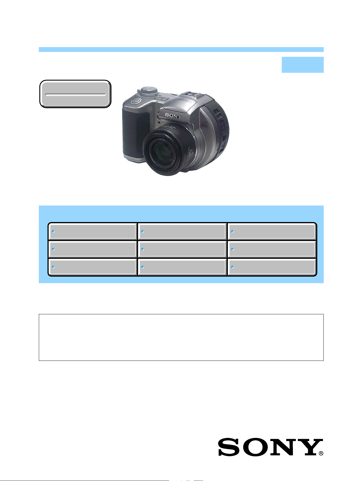
MVC-CD250/CD400
SERVICE MANUAL
Ver 1.0 2002. 04
Revision History
Revision History
Photo: MVC-CD400
Link
Link
SPECIFICATIONS
SPECIFICATIONS
BLOCK DIAGRAMS
BLOCK DIAGRAMS
LEVEL 2
US Model
Canadian Model
E Model
Chinese Model
Australian Model
Japanese Model
MVC-CD250/CD400
AEP Model
UK Model
Korea Model
Tourist Model
MVC-CD400
PRINTED WIRING BOARDS
PRINTED WIRING BOARDS
SERVICE NOTE
SERVICE NOTE
DISASSEMBLY
DISASSEMBLY
•For INSTRUCTION MANUAL, refer to SERVICE MANUAL, LEVEL 1 (992996841.pdf).
• This service manual contains information for Japanese model as well.
•Table for differences of function of each model
On the SY-76 board
This service manual procides the information that is premised
the circuit board replacement service and not intended repair
inside the SY-76 board.
Therefore, schematic diagram, printed wiring board and
electrical parts list of the SY-76 board are not shown.
The following pages are not shown.
FRAME SCHEMATIC DIAGRAMS
FRAME SCHEMATIC DIAGRAMS
SCHEMATIC DIAGRAMS
SCHEMATIC DIAGRAMS
SY-76 board
Schematic diagram ......................... Pages 4-15 to 4-40
Printed wiring board ........................ Pages 4-57 to 4-60
Electrical parts list ........................... Pages 6-15 to 6-23
The above-described information is shown in service
manual Level 3.
ADJUSTMENTS
ADJUSTMENTS
REPAIR PARTS LIST
REPAIR PARTS LIST
DIGITAL STILL CAMERA

MVC-CD250/CD400
COVER
COVER
System
Image device
Total pixels number of camera
Lens MVC-CD400
Camera
Effective pixels number of camera
Exposure control
White balance
Data formats
Recording media
Flash MVC-CD400
MVC-CD400
8.98 mm (1/1.8 type) color CCD
Primary color filter
MVC-CD250
6.64 mm (1/2.7 type) color CCD
Primary color filter
MVC-CD400
Approx. 4 130 000 pixels
MVC-CD250
Approx. 2 110 000 pixels
3 × zoom lens
f = 7.0 – 21.0 mm (9/32 – 27/32 inches)
(34 – 102 mm (1 3/8 – 4 1/8 inches)
when converted to a 35 mm still camera)
F2.0 – 2.5
MVC-CD250
3 × zoom lens
f = 6.4 – 19.2 mm (9/32 – 25/32 inches)
(41 – 123 mm (1 5/8 – 4 7/8 inches)
when converted to a 35 mm still camera)
F3.8 – 3.9
MVC-CD400
Approx. 3 950 000 pixels
MVC-CD250
Approx. 1 980 000 pixels
MVC-CD400
Automatic exposure, Shutter speed
priority, A perture priority,Manual
exposure, Scene selection (4 modes)
MVC-CD250
Automatic exposure, Scene selection
(3 modes)
Automatic, Daylight, Cloudy,
Fluorescent, Incandescent, One-push*
* MVC-CD400 only
Moving images: MPEG1
Still images: JPEG, GIF (for Clip
Motion), TIFF
Audio with still image: MPEG1
(Monaural)
8 cm CD-R/CD-RW
Recommended distance (ISO set to
Auto): 0.5 m to 5.0 m (19 3/4 inches to
196 7/8 inches)
MVC-CD250
Recommended distance (ISO set to
Auto): 0.8 m to 3.5 m (31 1/2 inches to
137 7/8 inches)
SPECIFICATIONS
Drive
Readout Non-contact optical readout (using
semiconductor laser)
Laser Wavelength: 779 to 789 nm
Maximum output: 23 mW
Input and Output connectors
A/V OUT (MONO) (Monaural)
Minijack
Video: 1 Vp-p, 75 Ω, unbalanced,
sync negative
Audio: 327 mV (at a 47 kΩ load)
Output impedance 2.2 kΩ
ACC jack Mini-minijack (ø 2.5 mm)
USB jack mini-B
LCD screen
Used LCD panel
6.2 cm (2.5 type) TFT drive
Total number of dots
123 200 (560 × 220) dots
General
Used battery pack
NP-FM50 (supplied)
Power requirements
7.2 V
Power consumption (during shooting
with LCD backlight on)
MVC-CD400
3.0 W
MVC-CD250
2.5 W
Operating temperature
0°C to +40°C (32°F to +104°F)
Storage temperature
–20°C to +60°C (–4°F to +140°F)
Dimensions
MVC-CD400
Approx. 138 × 95 × 103 mm
(5 1/2 × 3 3/4 × 4 1/8 inches)
(W/H/D, excluding maximum
protrusions)
MVC-CD250
Approx. 138 × 95 × 101 mm
(5 1/2 × 3 3/4 × 4 inches)
(W/H/D, excluding maximum
protrusions)
Mass MVC-CD400
Approx. 638 g (1 lb 7 oz) (including
battery pack NP-FM50, disc, and lens
cap)
MVC-CD250
Approx. 608 g (1 lb 6 oz) (including
battery pack NP-FM50, disc, and lens
cap)
AC-L10A/L10B AC power adaptor
Power requirements
100 to 240 V AC, 50/60 Hz
Rated output voltage
DC 8.4 V, 1.5 A in operating mode
Operating temperature
0°C to +40°C (32°F to +104°F)
Storage temperature
–20°C to +60°C (–4°F to +140°F)
Dimensions
125 × 39 × 62 mm
(5 × 1 9/16 × 2 1/2 inches) (w/h/d,
excluding maximum protrusions)
Mass Approx. 280 g (10 oz)
NP-FM50 battery pack
Used battery
Lithium-ion battery
Maximum voltage
DC 8.4 V
Nominal voltage
DC 7.2 V
Capacity 8.5 Wh (1 180 mAh)
Operating temperature
0°C to +40°C (32°F to +104°F)
Dimensions
38.2 × 20.5 × 55.6 mm
(1 9/16 × 13/16 × 2 1/4 inches) (w/h/d)
Mass Approx. 76 g (3 oz)
Accessories
•AC-L10A/L10B AC power adaptor (1)
•Power cord (mains lead) (1)
•USB cable (1)
•NP-FM50 battery pack (1)
•A/V connecting cable (1)
•8 cm CD adaptor (1)
•Mavica disc (7) (CD-R (6), CD-RW (1))
•Shoulder strap (1)
•Lens cap (1)
•Lens cap strap (1)
• CD-ROM (SPVD-009) (1)
•Operating instructions (1)
Design and specifications are subject to change
without notice.
— 2 —
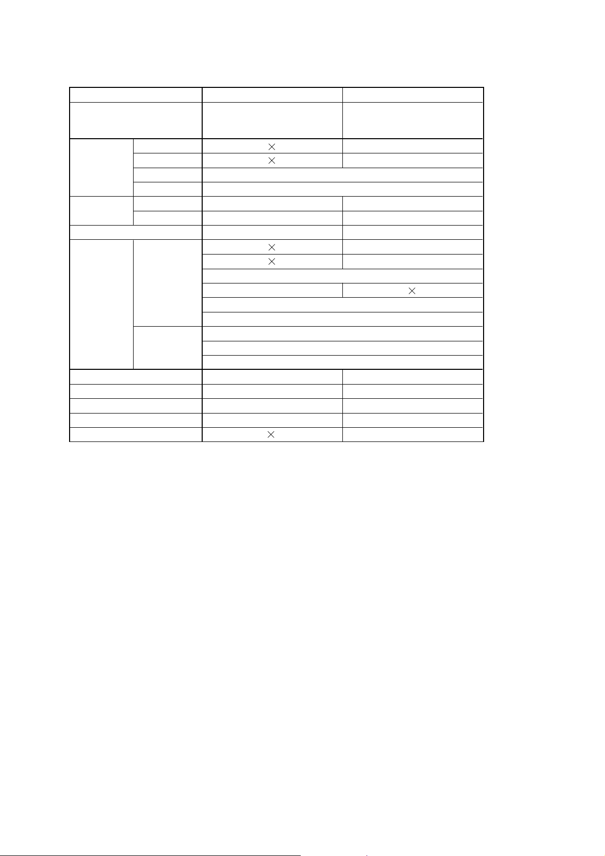
Table for differences of function
Model MVC-CD250 MVC-CD400
Destination
Carl Zeiss lens a
Lens
CCD imager
AF optical system AF illuminator (LED) Hologram AF (Laser diode)
Image size 1280 × 960
CD board CD-394 CD-393
FS board FS-85 FS-84
JK board JK-225 JK-224
PK board PK-66 PK-65
LS board LS-61
Movable lens a
Optical zoom 3 ×
Digital zoom 6 ×
Size 1/2.7 type 1/1.8 type
Pixels 2.1 mega 4.1 mega
Still
Movie 320 × 240
US, Canadian, E, Japanese,
Australian, Chinese
1600 × 1200
1600 (3:2)
640 × 480
320 (HQ)
160 × 112
US, Canadian, AEP, UK, E
Japanese, Australian, Chinese,
Korea, Tour ist
2272 × 1704
2272 (3:2)
MVC-CD250/CD400
,
— 3 —

MVC-CD250/CD400
WARNING!!
WHEN SERVICING, DO NOT APPROACH THE LASER
EXIT WITH THE EYE TOO CLOSELY. IN CASE IT IS
NECESSARY TO CONFIRM LASER BEAM EMISSION,
BE SURE T O OBSERVE FR OM A DIST ANCE OF MORE
THAN 30 cm FROM THE SURFACE OF THE
OBJECTIVE LENS ON THE OPTICAL PICK-UP BLOCK.
SAFETY-RELATED COMPONENT WARNING!!
COMPONENTS IDENTIFIED BY MARK 0 OR DOTTED LINE WITH
MARK 0 ON THE SCHEMATIC DIAGRAMS AND IN THE PARTS
LIST ARE CRITICAL TO SAFE OPERATION. REPLACE THESE
COMPONENTS WITH SONY PARTS WHOSE PART NUMBERS
APPEAR AS SHOWN IN THIS MANUAL OR IN SUPPLEMENTS
PUBLISHED BY SONY.
CAUTION:
The use of optical instrument with this product will increase eye
hazard.
CAUTION
Use of controls or adjustments or performance of procedures
other than those specified herein may result in hazardous
radiation exposure.
ATTENTION AU COMPOSANT AYANT RAPPORT
À LA SÉCURITÉ!
LES COMPOSANTS IDENTIFÉS P AR UNE MARQUE 0 SUR LES
DIAGRAMMES SCHÉMA TIQUES ET LA LISTE DES PIÈCES SONT
CRITIQUES POUR LA SÉCURITÉ DE FONCTIONNEMENT. NE
REMPLACER CES COMPOSANTS QUE PAR DES PIÈSES SONY
DONT LES NUMÉROS SONT DONNÉS DANS CE MANUEL OU
DANS LES SUPPÉMENTS PUBLIÉS PAR SONY.
SAFETY CHECK-OUT
After correcting the original service problem, perform the following
safety checks before releasing the set to the customer.
1. Check the area of your repair for unsoldered or poorly-soldered
connections. Check the entire board surface for solder splashes
and bridges.
2. Check the interboard wiring to ensure that no wires are
"pinched" or contact high-wattage resistors.
3. Look for unauthorized replacement parts, particularly
transistors, that were installed during a previous repair . Point
them out to the customer and recommend their replacement.
4. Look for parts which, through functioning, show obvious signs
of deterioration. Point them out to the customer and
recommend their replacement.
5. Check the B+ voltage to see it is at the values specified.
6. Flexible Circuit Board Repairing
•Keep the temperature of the soldering iron around 270˚C
during repairing.
• Do not touch the soldering iron on the same conductor of the
circuit board (within 3 times).
• Be careful not to apply force on the conductor when soldering
or unsoldering.
Unleaded solder
Boards requiring use of unleaded solder are printed with the leadfree mark (LF) indicating the solder contains no lead.
(Caution: Some printed circuit boards may not come printed with
the lead free mark due to their particular size.)
: LEAD FREE MARK
Unleaded solder has the following characteristics.
• Unleaded solder melts at a temperature about 40°C higher than
ordinary solder.
Ordinary soldering irons can be used but the iron tip has to be
applied to the solder joint for a slightly longer time.
Soldering irons using a temperature regulator should be set to
about 350°C.
Caution: The printed pattern (copper foil) may peel away if the
heated tip is applied for too long, so be careful!
• Strong viscosity
Unleaded solder is more viscous (sticky, less prone to flow) than
ordinary solder so use caution not to let solder bridges occur such
as on IC pins, etc.
• Usable with ordinary solder
It is best to use only unleaded solder but unleaded solder may
also be added to ordinary solder.
— 4 —

MVC-CD250/CD400
TABLE OF CONTENTS
Section Title Page Section Title Page
1. SERVICE NOTE
1-1. Note for Repair ································································1-1
1-2. Discharging of the FLASH unit’s Charging Capacitor ··· 1-1
1-2-1.Preparing the Short Jig ····················································1-1
1-2-2.Discharging the Capacitor ···············································1-1
1-3. Notes on Handling the Laser Diode
[Laser Unit (D9001: MVC-CD400) and
Base Unit (DDX-G3000)] ··················································1-2
1-3-1.Precautions for Checking Emission of Laser Diode
[Base Unit (DDX-G3000)] ··············································1-2
1-3-2.Soldering Conditions of Laser Unit
(D9001: MVC-CD400) ···················································1-2
1-4. Description on Self-diagnosis Display ····························1-3
1-5. Power Supplying Method ················································1-3
2. DISASSEMBLY .........................................................2-1
2-1. Side Cabinet Block Assembly ·········································2-2
2-2. Cabinet (Rear) Block Assembly······································2-2
2-3. Lens Block Assembly······················································2-3
2-4. Stroboscope Block Assembly··········································2-4
2-5. Flash Unit ········································································2-5
2-6. BT Holder Assembly·······················································2-5
2-7. SY-76 Board ····································································2-6
2-8. DDX-G3000 Complete Assembly···································2-7
2-9. Base Unit ·········································································2-7
2-10. PK-65/66 Board·······························································2-8
2-11. LCD Module···································································· 2-9
2-12. Circuit Boards Locaion ·················································2-10
2-13. Flexible Boards Locaion ···············································2-11
3. BLOCK DIAGRAMS
3-1. Overall Block Diagram ···················································3-1
3-10. Power Block Diagram 1 ················································3-19
3-11. Power Block Diagram 2 ················································3-21
4. PRINTED WIRING BOARDS AND
SCHEMATIC DIAGRAMS
4-1. Frame Schematic Diagrams
Frame Schematic Diagram (1/2) ·····································4-1
Frame Schematic Diagram (2/2) ·····································4-3
4-2. Schematic Diagrams························································4-5
CD-393 (1/2) (CCD IMAGER)
(MVC-CD400)································································4-7
CD-393 (2/2) (CAMERA MODULE)
(MVC-CD400)································································4-9
CD-394 (1/2) (CCD IMAGER)
(MVC-CD250)······························································4-11
CD-394 (2/2) (CAMERA MODULE)
(MVC-CD250)······························································4-13
PK-65/66 (1/2)
(LCD DRIVE, TIMING GENERATOR) ·····················4-41
PK-65/66 (2/2) (BACK LIGHT DRIVE) ·····················4-43
FS-84/85 (DC IN, CONTROL SWITCH) ····················4-45
JK-224/225 (JACK) ······················································4-47
LS-61 (LENS CAP SWITCH) (MVC-CD400) ············4-49
CONTROL SWITCH BLOCK (ZK-860/880) ·············4-50
4-3. Printed Wiring Boards ···················································4-51
CD-393 (MVC-CD400) ················································4-53
CD-394 (MVC-CD250) ················································4-55
PK-65/66 ·······································································4-61
FS-84/85 ········································································4-65
JK-224/225 ····································································4-67
LS-61 (MVC-CD400) ···················································4-69
FP-482/489/490 ·····························································4-71
4-4. Waveforms·····································································4-73
4-5. Mounted Parts Location ················································4-78
5. ADJUSTMENTS
1-1. Adjusting Items when Replacing
Main Parts and Boards ····················································5-2
5-1. Camera Section Adjustments··········································· 5-3
1-1. Preparations Before Adjustment
1-1-1.List of Service Tools························································5-3
1-1-2.Preparations ·····································································5-4
1-1-3.Discharging of the Flashlight Power Supply···················5-4
1-1-4.Precaution
1. Setting the Switch ····························································5-6
2. Order of Adjustments ······················································5-6
3. Subjects ··········································································· 5-6
4. Preparing the Flash Adjustment Box·······························5-7
1-2. Initialization of A, B, D, E, F, 7, 9 Page Data
1-2-1.Initialization of A, D Page Data
1. Initializing A, D Page Data··············································5-8
2. Modification of A, D Page Data ······································5-8
3. A Page Table····································································5-8
4. D Page Table····································································5-8
1-2-2.Initialization of B, E, F, 7, 9 Page Data
1. Initializing B, E, F, 7, 9 Page Data ··································5-9
2. Modification of B, E, F, 7, 9 Page Data···························5-9
3. B Page Table···································································· 5-9
4. E Page Table ····································································5-9
5. F Page Table ··································································5-10
6. 7 Page Table···································································5-12
7. 9 Page Table···································································5-12
1-3. Video System Adjustment
1. Video Output Level Adjustment ····································5-13
1-4. Camera System Adjustments·········································5-14
Data Setting During Camera System Adjustments········5-14
Picture Frame Setting ····················································5-15
Check on the Oscilloscope ············································5-15
1. Hall Adjustment (MVC-CD250 only) ···························5-16
2. Flange Back Adjustment
(Using the minipattern box) ··········································5-17
3. Flange Back Adjustment
(Using the flange back adjustment chart
and subject more than 500 m away) ······························5-18
4. Flange Back Check ························································5-19
5. F No. Compensation ······················································5-19
6. Mechanical Shutter Adjustment ····································5-20
7. Light Value Adjustment·················································5-20
8. Mixed Color Cancel Adjustment ···································5-21
9. Auto White Balance 3200K Standard Data Input 1 ······5-21
10. Auto White Balance 3200K Standard Data Input 2 ······5-22
11. Auto White Balance 3200K Standard Data Input 3 ······5-22
12. Auto White Balance 3200K Check 1 ····························5-23
13. Auto White Balance 3200K Check 2 ····························5-24
14. Auto White Balance 3200K Check 3 ····························5-24
15. Auto White Balance 5800K Standard Data Input 1 ······5-25
16. Auto White Balance 5800K Standard Data Input 2 ······5-26
17. Auto White Balance 5800K Standard Data Input 3 ······5-26
18. Auto White Balance 5800K Check 1 ····························5-27
19. Auto White Balance 5800K Check 2 ····························5-28
20. Auto White Balance 5800K Check 3 ····························5-29
21. Color Reproduction Adjustment····································5-30
22. CCD White Defect Compensation ································5-31
23. CCD Black Defect Compensation································· 5-32
24. CCD Linearity Check ····················································5-33
25. Strobe White Balance Adjustment·································5-34
26. AF Illumination Check (MVC-CD250 only) ················5-36
1-5. LCD System Adjustments ·············································5-37
— 5 —

MVC-CD250/CD400
Section Title Page
1. LCD Initial Data Input (1) ·············································5-38
2. LCD Initial Data Input (2) ·············································5-38
3. Back Light Adjustment (PK-65/66 Board)····················5-39
4. VCO Adjustment (PK-65/66 Board) ·····························5-39
5. D Range Adjustment (PK-65/66 Board) ·······················5-40
6. Contrast Adjustment (PK-65/66 Board) ························5-40
7. V-COM Level Adjustment (PK-65/66 Board)···············5-41
8. V-COM Adjustment (PK-65/66 Board)·························5-41
9. White Balance Adjustment (PK-65/66 Board)··············5-42
1-6. System Control System Adjustments
1. Battery Down Adjustment ·············································5-43
2. Serial No. Input ·····························································5-44
5-2. Service Mode
2-1. Adjusting Remote Commander ·····································5-45
1. Used the Adjusting Remote Commander ······················5-45
2. Precautions upon Using the Adjusting
Remote Commander······················································5-45
2-2. Data Process ··································································5-46
2-3. Service Mode
1. Setting the Test Mode····················································5-47
2. Bit Value Discrimination ···············································5-47
3. Switch Check (1) ···························································5-48
4. Switch Check (2) ···························································5-48
5. Switch Check (3) (MVC-CD400 only) ·························5-48
6. Switch Check (4) ···························································5-49
7. Switch Check (5) ···························································5-49
8. Switch Check (6) ···························································5-49
9. LED Check ····································································5-50
10. Self Diagnosis Log Check·············································5-50
11. Record of Use Check·····················································5-50
6. REPAIR PARTS LIST
6-1. Exploded Vie ws ·······························································6-1
6-1-1.Overall Assembly ····························································6-1
6-1-2.Cabinet (Front) Block Assembly (MVC-CD250) ···········6-2
6-1-3.Cabinet (Front) Block Assembly (MVC-CD400) ···········6-3
6-1-4.Lens Block Assembly (MVC-CD250) ····························6-4
6-1-5.Lens Block Assembly (MVC-CD400) ····························6-5
6-1-6.Stroboscope Block Assembly··········································6-6
6-1-7.DDX-G3000 Complete Assembly···································6-7
6-1-8.Side Cabinet Assembly····················································6-8
6-1-9.Cabinet (Rear) Block Assembly ······································6-9
6-2. Electrical Parts List ·······················································6-10
* The color reproduction frame is shown on page 147.
— 6 —
MVC-CD250/CD400
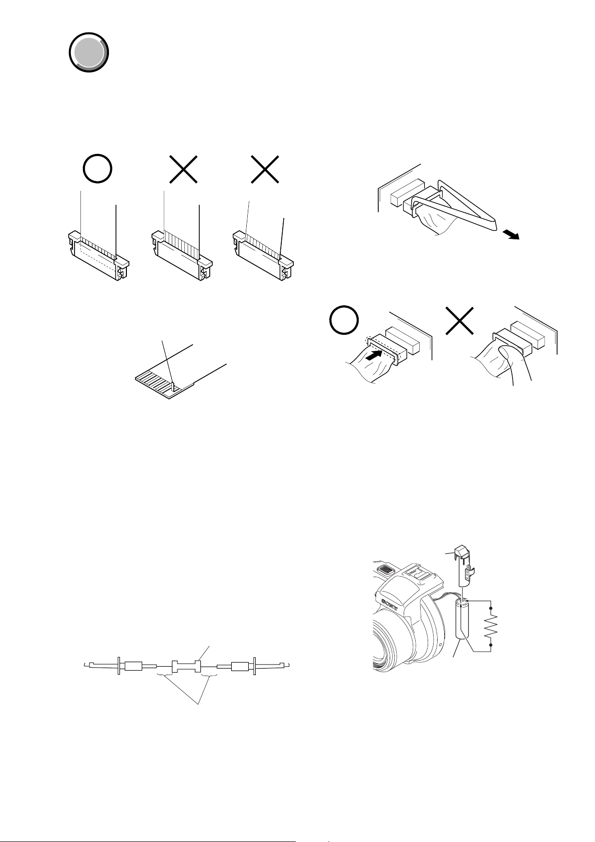
When installing a connector, don’t press down at wire of connector.
It is possible that a wire is snapped.
COVER
COVER
SECTION 1
SERVICE NOTE
1-1. NOTE FOR REPAIR
Make sure that the flat cable and flexible board are not cracked of
bent at the terminal.
Do not insert the cable insufficiently nor crookedly.
Cut and remove the part of gilt
which comes off at the point.
(Be careful or some
pieces of gilt may be left inside)
When remove a connector, don’t pull at wire of connector.
It is possible that a wire is snapped.
1-2. DISCHARGING OF THE FLASH UNIT’S CHARGING CAPACITOR
The charging capacitor of the Flash unit is charged up to the
maximum 300 V potential.
There is a danger of electric shock by this high voltage when the
battery is handled by hand. The electric shock is caused by the
charged voltage which is kept without discharging when the main
power of the unit is simply turned off. Therefore, the remaining
voltage must be discharged as described below.
1-2-1. Preparing the Short Jig
To preparing the short jig, a small clip is attached to each end of a
resistor of 1 kΩ /1 W (1-215-869-11).
Wrap insulating tape fully around the leads of the resistor to prevent
electrical shock.
1 kΩ/1 W
Wrap insulating tape.
1-2-2. Discharging the Capacitor
Short-circuit between the positive and the negative terminals of
charged capacitor with the short jig about 10 seconds.
Capacitor retainer
R: 1 kΩ/1 W
(Part code:
1-215-869-11)
Capacitor
1-1
MVC-CD250/CD400
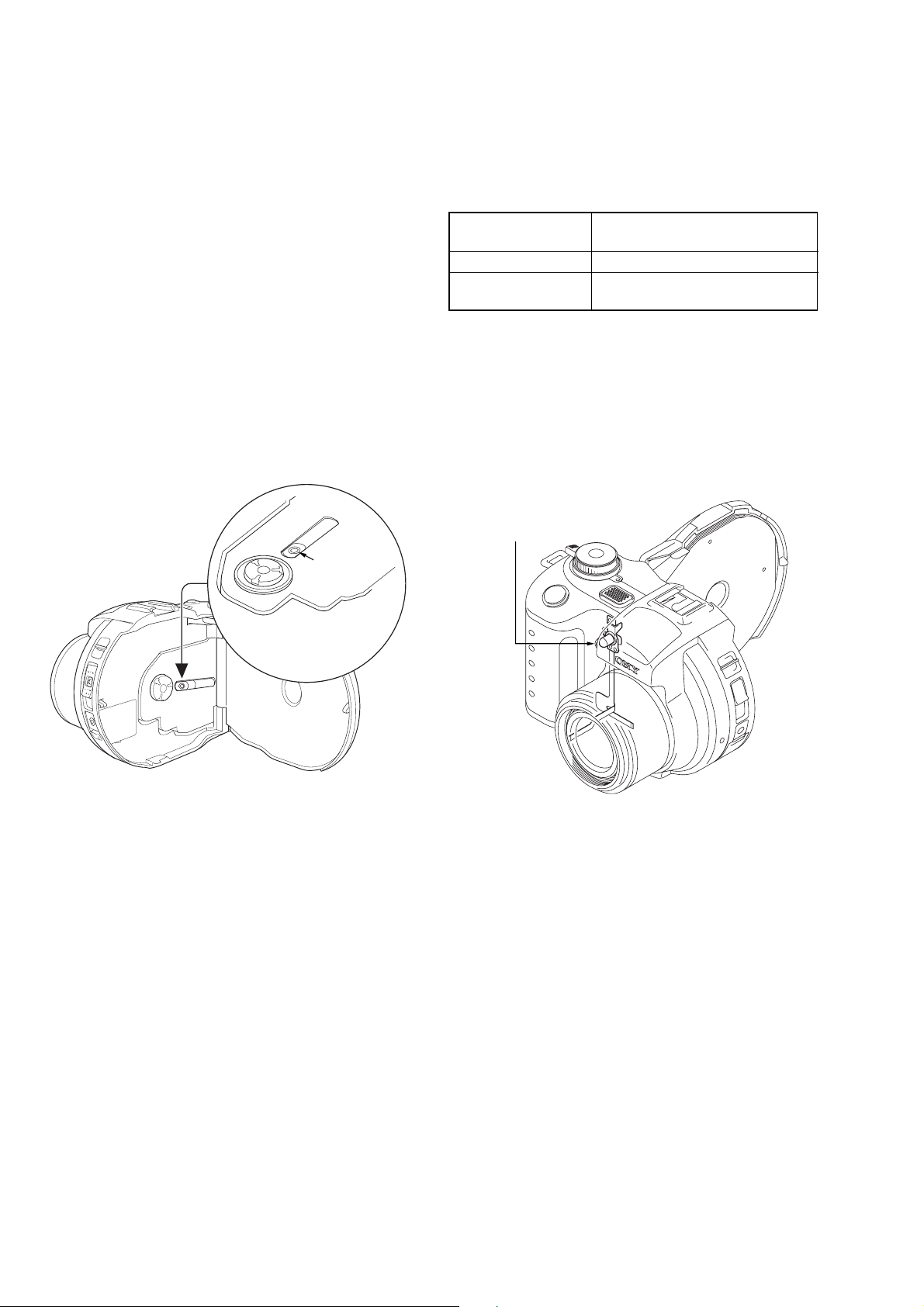
1-3. NOTES ON HANDLING THE LASER DIODE
[LASER UNIT (D9001: MVC-CD400) AND BASE UNIT (DDX-G3000)]
The laser diode may suffer electrostatic breakdown because of the
potential difference generated by the charged electrostatic load, etc.
on clothing and the human body.
During repair, pay attention to electrostatic breakdown and also use
the procedure in the printed matter which is included in the repair
parts.
The flexible board is easily damaged and should be handled with
care.
1-3-1. Precaution for Checking Emission of Laser
Diode [Base Unit (DDX-G3000)]
Laser light of the equipment is focused by the object lens in the
optical pick-up so that the light focuses on the reflection surface of
the disc. Therefore, be sure to keep your eyes more then 30 cm
apart from the object lens when you check the emission of laser
diode.
Optical pick-up
(Laser diode)
1-3-2. Soldering Conditions of Laser Unit
(D9001: MVC-CD400)
Temperature of
the Soldering Iron
Time to Solder 3 seconds
Interval to Solder
Laser unit
(D9001)
350 °C
Next terminal is soldered after
waiting for 1 second
[MVC-CD400]
1-2
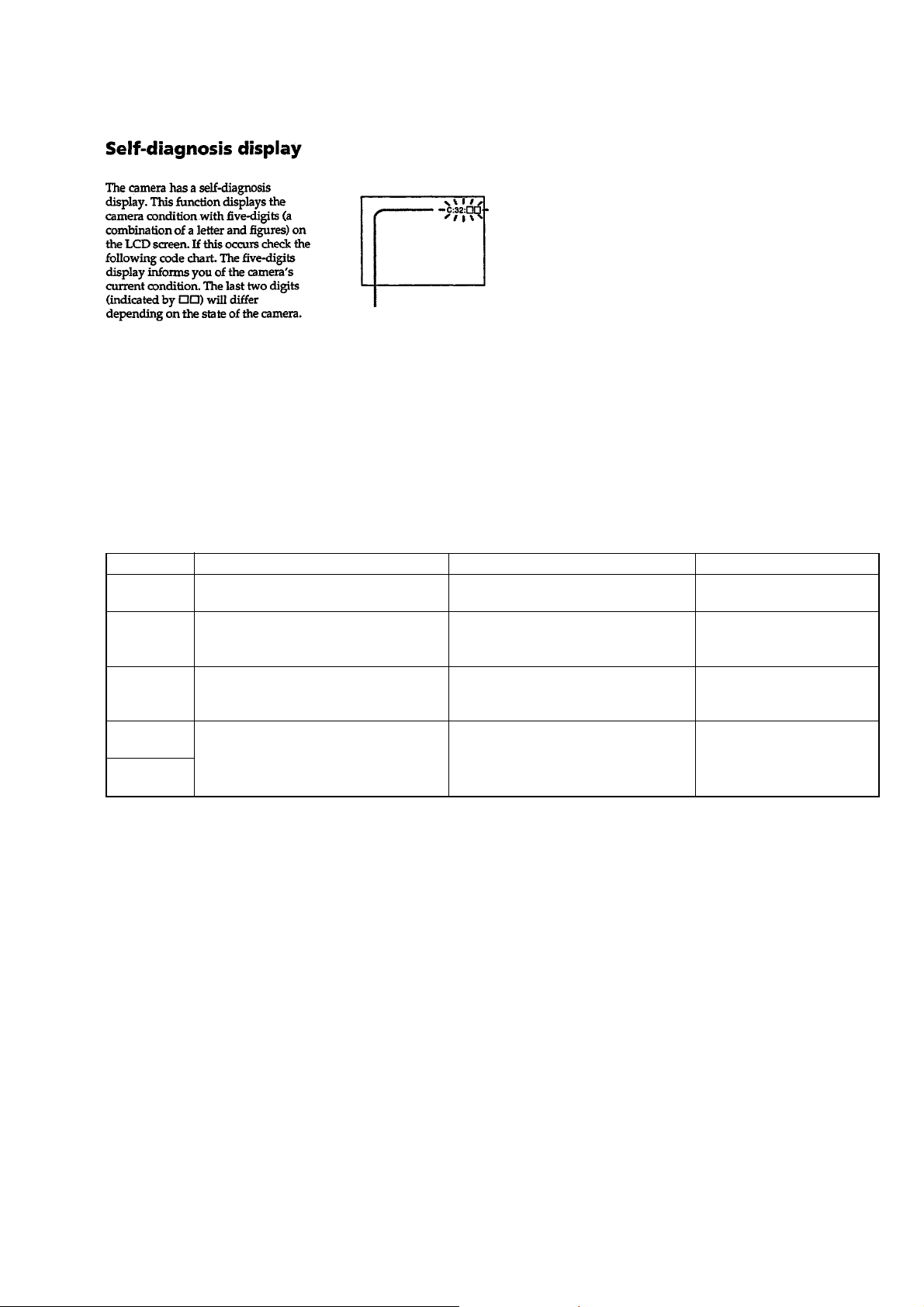
1-4. DESCRIPTION ON SELF-DIAGNOSIS DISPLAY
Self-diagnosis display
• C: ss: ss
You can reverse the camera
malfunction yourself. (However,
contact your Sony dealer or local
authorized Sony service facility
when you cannot recover from the
camera malfunction.)
• E: ss: ss
Contact your Sony dealer or local
authorized Sony service facility.
MVC-CD250/CD400
Display Code
C:32:01
C:13:01
E:91:01
*1
E:61:00
*1
E:61:10
Note: The error code is cleared if the battery is removed.
*1 : The error display is given in two ways.
Change the disk and turn off the main
power then back on.
Replace the CD-R/RW disk.
Checking of flash unit or replacement of
flash unit
Checking of lens drive circuit
Countermeasure
Cause
Defective base unit.
• The type of CD-R/RW disk that cannot
be used by this machine, is inserted.
• Data is damaged.
Abnormality when flash is being
charged.
When failed in the focus initialization.
1-5. POWER SUPPLYING METHOD
Use the AC power adaptor (AC-L10A/L10B) when supplying the power to this set.
Caution Display During Error
DRIVE ERROR
DISK ERROR
Flash LED
Flash display
Flashing at 3.2 Hz
—
1-3E
1-3
MVC-CD250/CD400
COVER
COVER
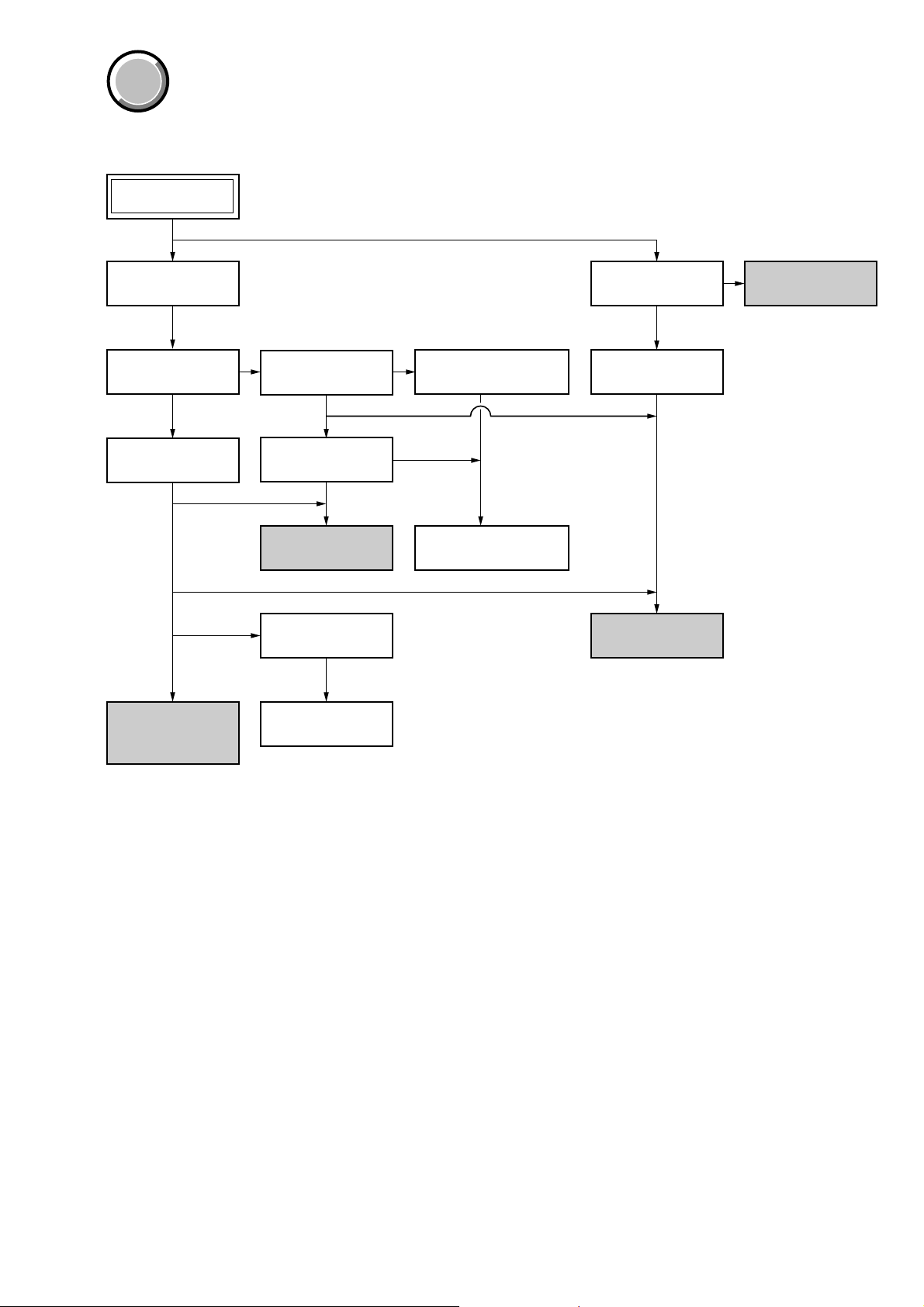
• This set can be disassembled in the order shown below.
MVC-CD250/CD400
2-1. SIDE CABINET
BLOCK ASSEMBLY
(Page 2-2)
2-2. CABINET (REAR)
BLOCK ASSEMBLY
(Page 2-2)
2-3. LENS BLOCK
ASSEMBLY
(Page 2-3)
2-6. BT HOLDER
ASSEMBLY
(Page 2-5)
2-7. SY-76 BOARD
(Page 2-6)
SECTION 2
DISASSEMBLY
2-8. DDX-G3000 COMPLETE
ASSEMBLY
(Page 2-7)
2-10.PK-65/66 BOARD
(Page 2-8)
2-11.LCD MODULE
(Page 2-9)
SERVICE POSITION
(PK-65/66 BOARD:
SIDE A) (Page 2-8)
SERVICE POSITION
(CD-393/394 BOARD,
SY-76 BOARD: SIDE A)
(Page 2-4)
SERVICE POSITION
(SY-76 BOARD: SIDE B)
(Page 2-6)
2-4. STROBOSCOPE
BLOCK ASSEMBLY
(Page 2-4)
2-5. FLASH UNIT
(Page 2-5)
2-9. BASE UNIT
(Page 2-7)
SERVICE POSITION
(PK-65/66 BOARD:
SIDE B) (Page 2-9)
2-1
MVC-CD250/CD400
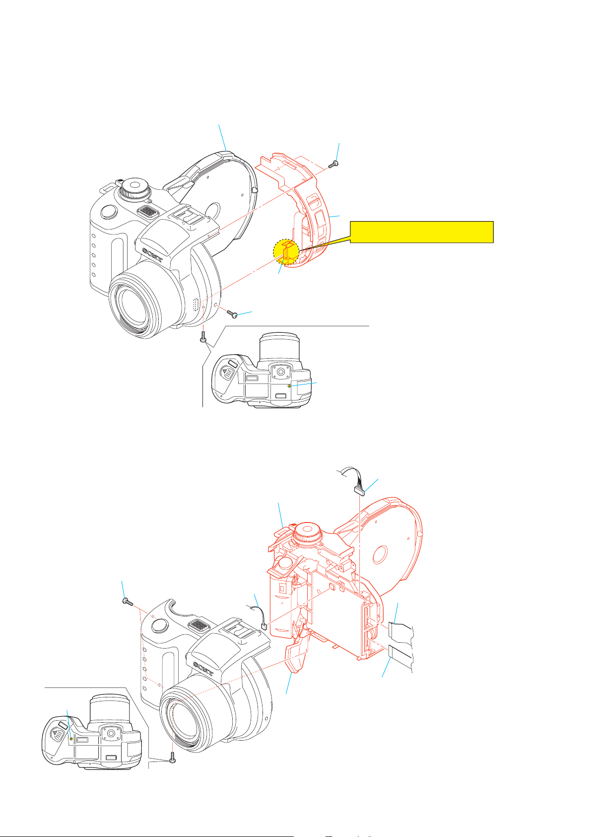
Note: Follow the disassembly procedure in the numerical order given.
2-1. SIDE CABINET BLOCK ASSEMBLY
3 Open the CD cabinet.
4 Two screws (M2)
5 Side cabinet block assembly
Note:Remove it while taking care as
the flexible board is connected.
6 FP-482 flexible board
(CN718)
1 Screw (M2)
2-2. CABINET (REAR) BLOCK ASSEMBLY
6 Cabinet (rear) block assembly
3 Two screws (M2)
8 Harness (microphone)
(CN702)
2 Screw (M2)
7 Harness (SS-084)
(CN719)
1 FP-484 flexible board
(CN724)
4 Screw
(M2)
5 Open the battery lid.
2-2
2 FP-485/FP-486 flexible board
(CN651)
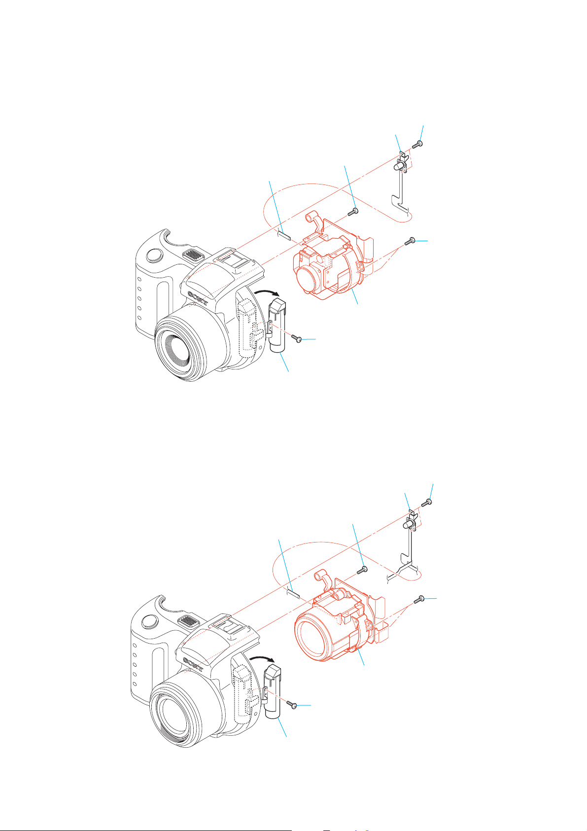
2-3. LENS BLOCK ASSEMBLY
(MVC-CD250)
MVC-CD250/CD400
1 FP-489 flexible board
(CN502)
5 Capacitor
3 AF/self timer illuminator
6 Screw
(M1.7
× 5)
8 Lens block assembly
4 Screw
(M1.7
× 5)
2 Two screws
(M1.7 × 5)
7 Two screws
(M1.7
× 5)
(MVC-CD400)
1 FP-490 flexible board
(CN502)
4 Screw
6 Screw
(M1.7
3 Laser unit
(M1.7 × 5)
8 Lens block assembly
× 5)
2 Two screws
(M1.7 × 5)
7 Two screws
(M1.7
× 5)
5 Capacitor
2-3
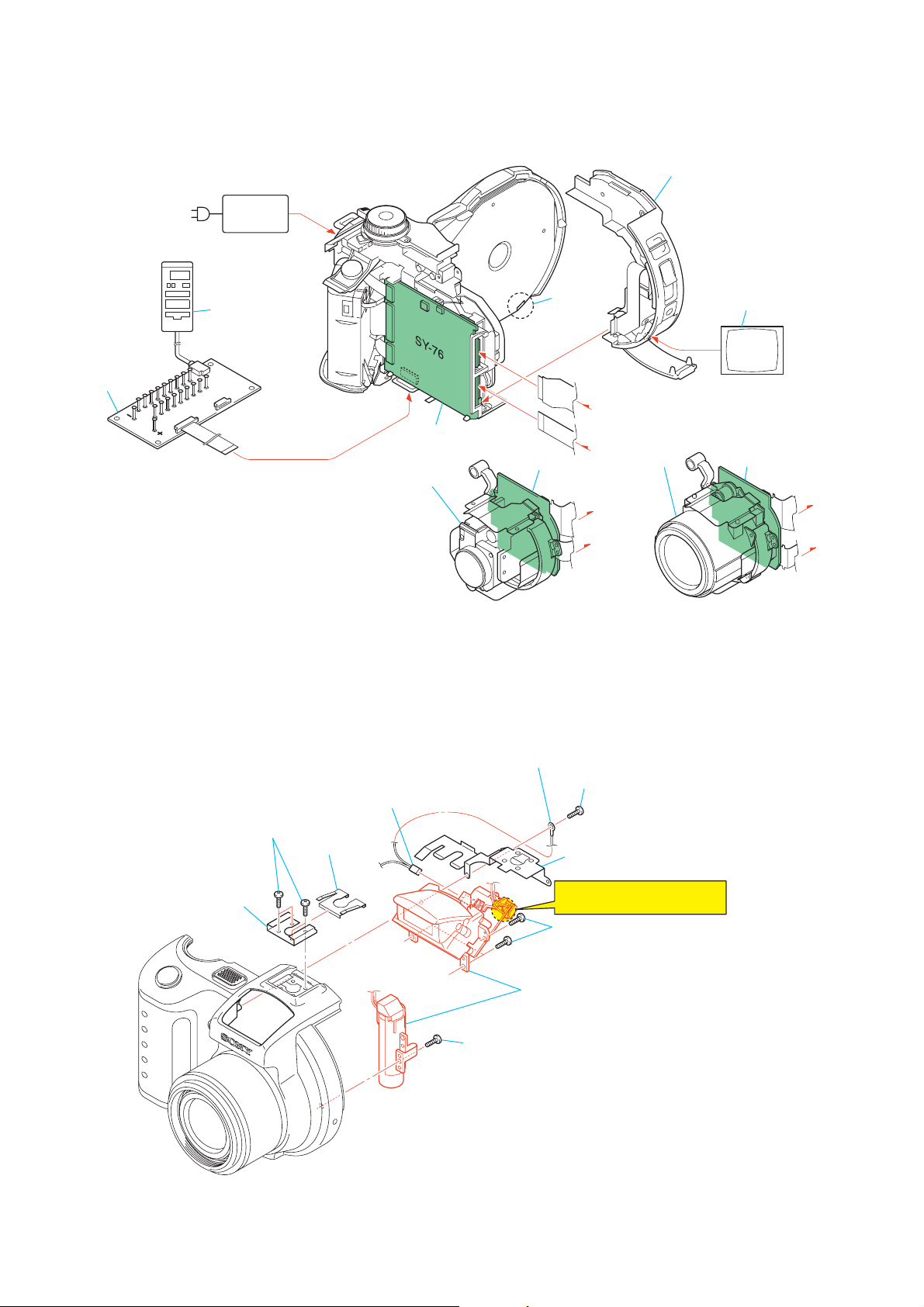
MVC-CD250/CD400
[SERVICE POSITION (CD-393/394 BOARD, SY-76 BOARD: SIDE A)]
Side cabinet block assembly
DC-IN
CPC-9 jig
(J-6082-393-C)
(Note 1, 2)
1
Note 1: Don’t use the 12 pin flexible board of CPC-9 jig.
It causes damage to the unit.
Note 2: The old CPC-9 jig (Parts code: J-6082-393-B) Cannot be used,
because it cannot operate the adjustment remote commander.
Note 3: Must be pressed lid open/close detect switch (S307, S308 on
PK-65/66 board) when using the CD-R/RW drive unit.
AC power
adaptor
Adjustment remote
commander
18
1
18
SY-76 board
Lens block assembly
(MVC-CD250)
S307, S308
(Note 3)
CD-394 board
A
B
Lens block assembly
(MVC-CD400)
A
B
Monitor
CD-393 board
A
B
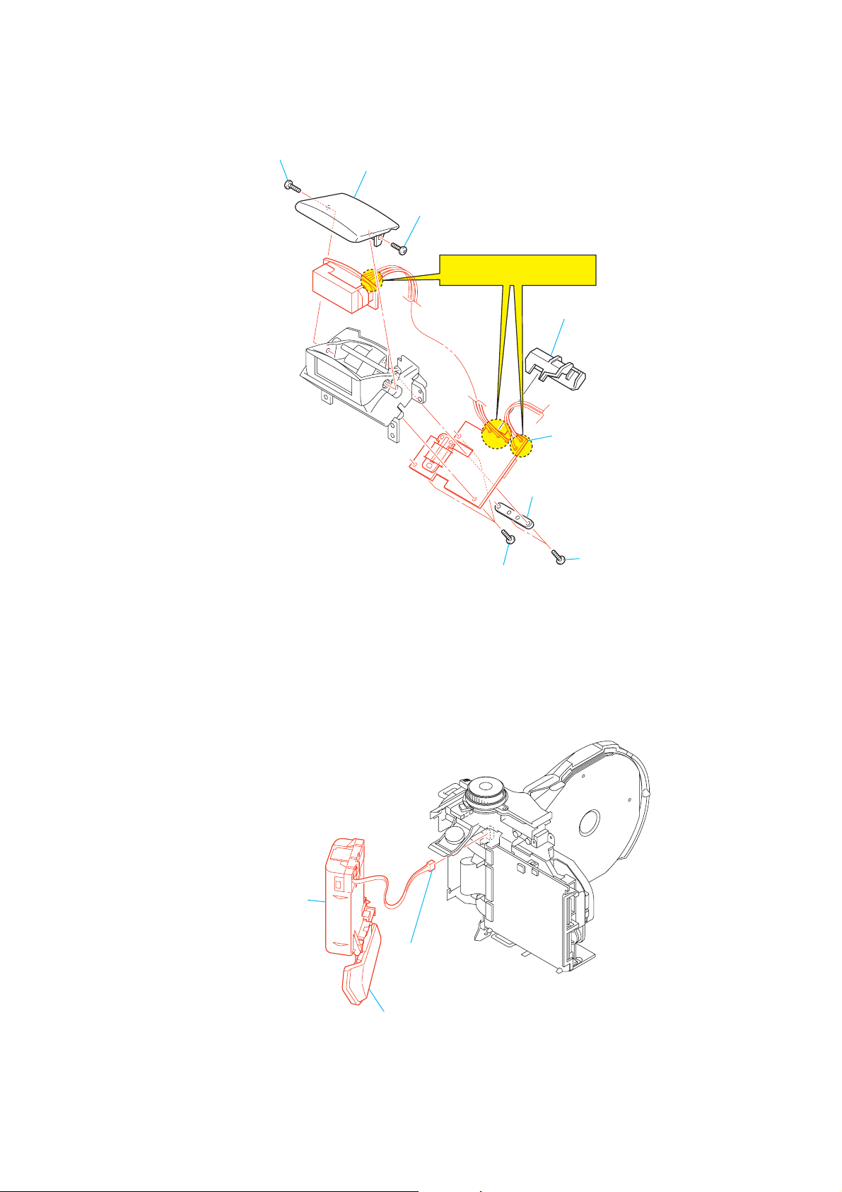
2-4. STROBOSCOPE BLOCK ASSEMBLY
4 Stroboscope terminal conector
(MVC-CD400 only)
2 Four screws
(M1.7)
1 Shoe spring
3 Shoe
6 Earth lug
(MVC-CD400 only)
0 Stroboscope block
8 Screw
(M1.7
×
5)
5 Screw
(M1.7
×
5)
7 Shoe stiffner
Note:High-voltage cautions.
(See page 1-1)
9 Three screws
(M1.7
×
5)
assembly
2-4
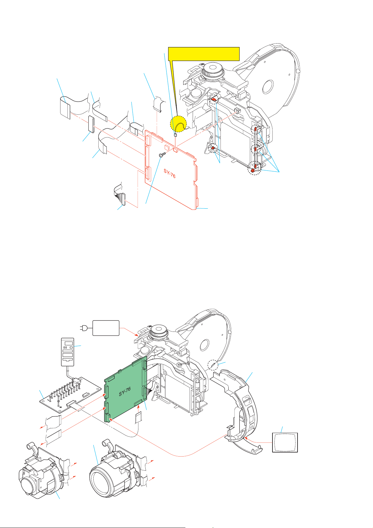
2-5. FLASH UNIT
1 Screw
(M1.7
MVC-CD250/CD400
×
4)
3 St roof cover
2 Screw
×
4)
(M1.7
Note:High-voltage cautions.
(See page 1-1)
6 Three screws
(M1.7
×
4)
7 Harness cover
8 Flash unit
5 ST solenoid cover
4 Two screws
(M1.7
×
4)
2-6. BT HOLDER ASSEMBLY
2 BT holder assembly
3 Connector
(CN003)
1 Open the battery lid.
2-5
MVC-CD250/CD400
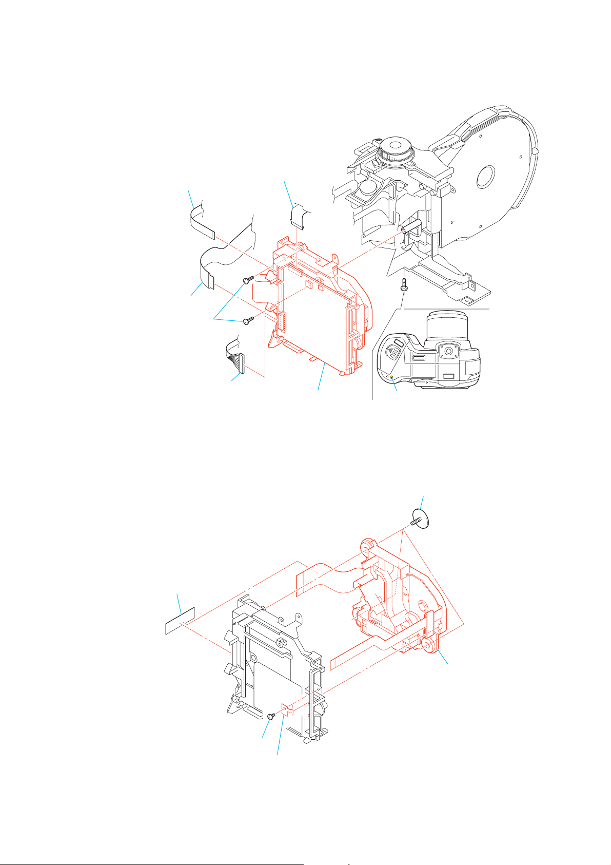
2-7. SY-76 BOARD
5 FP-488 flexible board
(CN901)
2 FP-481 flexible board
(CN721)
6 Ferrite core
3 FP-483 flexible board
(CN717)
4 FS-141 harness
(CN001)
7 Harness (microphone)
(CN902)
1 Control switch block
(CN720)
qs Flexible board
(base unit) (CN902)
Note:Don't pull at harness of
8 Screw (M2)
connector.
9 Two claws
0 Four claws
qa SY-76 board
[SERVICE POSITION (SY-76 BOARD: SIDE B)]
Setting the "Forced Power ON mode"
[Forced CAMERA mode]
1) Select page: 0, address: 01, and set
data: 01.
2) Select page: D, address: 2F, set data:
00, and then press the PAUSE button
of adjustment remote commander.
3) Select page: D, address: 21, set data:
07, and then press the PAUSE button
of adjustment remote commander.
4) Turn the power off, then on again.
DC-IN
CPC-9 jig
(J-6082-393-C)
(Note 1, 2)
18
1
A
AC power
adaptor
Adjustment remote
commander
[Forced PLAY mode]
1) Select page: 0, address: 01, and set
data: 01.
2) Select page: D, address: 2F, set data:
00, and then press the PAUSE button
of adjustment remote commander.
3) Select page: D, address: 21, set data:
08, and then press the PAUSE button
of adjustment remote commander.
4) Turn the power off, then on again.
18
1
SY-76 board
Exiting the "Forced Power ON mode"
1) Select page: 0, address: 01, and set
data: 01.
2) Select page: D, address: 2F, set data:
E0, and then press the PAUSE button
of adjustment remote commander.
3) Select page: D, address: 21, set data:
00, and then press the PAUSE button
of adjustment remote commander.
4) Select page: 0, address: 01, and set
data: 00.
S307, S308
(Note 3)
Side cabinet block assembly
Monitor
B
Lens block assembly
(MVC-CD400)
Lens block assembly
(MVC-CD250)
A
B
A
B
Note 1: Don't use the 12 pin flexible board of CPC-9 jig.
It causes damage to the unit.
Note 2: The old CPC-9 jig (Parts code: J-6082-393-B) Cannot be used,
because it cannot operate the adjustment remote commander.
Note 3: Must be pressed lid open/close detect switch (S307, S308 on
PK-65/66 board) when using the CD-R/RW drive unit.
2-6
2-8. DDX-G3000 COMPLETE ASSEMBLY
MVC-CD250/CD400
2 FP-481 flexible board
3 FP-483 flexible board
(CN717)
5 Two screws
2-9. BASE UNIT
(CN721)
(M1.7
× 5)
4 FS-141 harness
(CN001)
1 Control switch block
(CN720)
7 DDX-G3000 complete assembly
6 Screw (M2)
3 Tape
4 Three special
head screws
5 Base unit
1 Screw (M2)
2 Flexible board
2-7
MVC-CD250/CD400
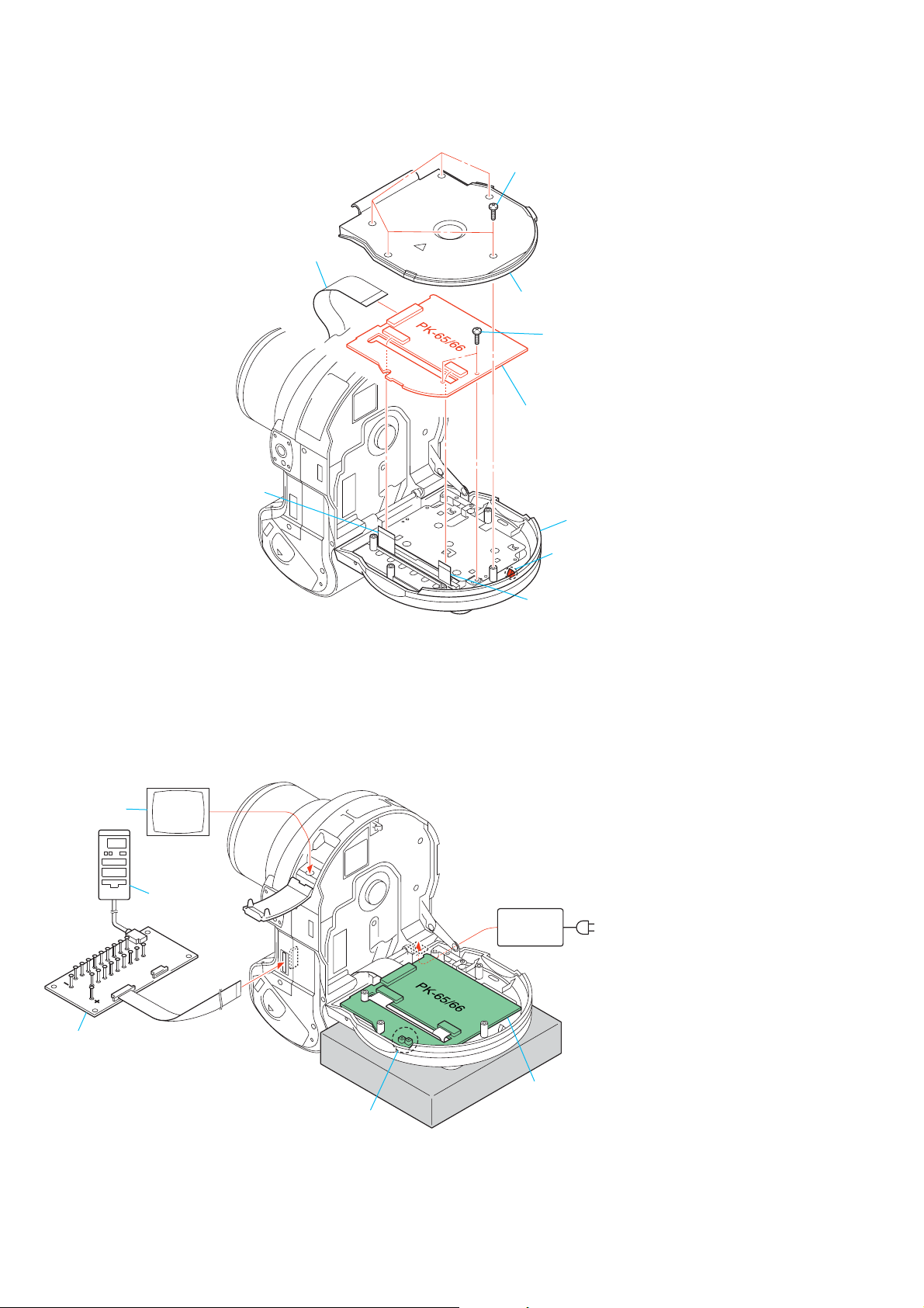
2-10.PK-65/66 BOARD
2 Five screws
(M1.7 × 5)
5 FP-483 flexible board
(CN303)
4 CD cabinet lid assembly
6 LCD flexible board
(CN302)
[SERVICE POSITION (PK-65/66 BOARD: SIDE A)]
Note 1: Don’t use the 12 pin flexible board of CPC-9 jig.
It causes damage to the unit.
Note 2: The old CPC-9 jig (Parts code: J-6082-393-B) Cannot be used,
because it cannot operate the adjustment remote commander.
Monitor
Note 3: Must be pressed lid open/close detect switch (S307, S308 on
PK-65/66 board) when using the CD-R/RW drive unit.
8 Two screws
9 PK-65/66 board
7 Back light flexible board
(CN201)
× 4)
(M1.7
1 Open the CD cabinet.
3 Claw
18
1
CPC-9 jig
(J-6082-393-C)
(Note 1, 2)
Adjustment remote
commander
1
18
S307, S308
(Note 3)
2-8
AC power
adaptor
PK-65/66 board
DC-IN
2-11.LCD MODULE
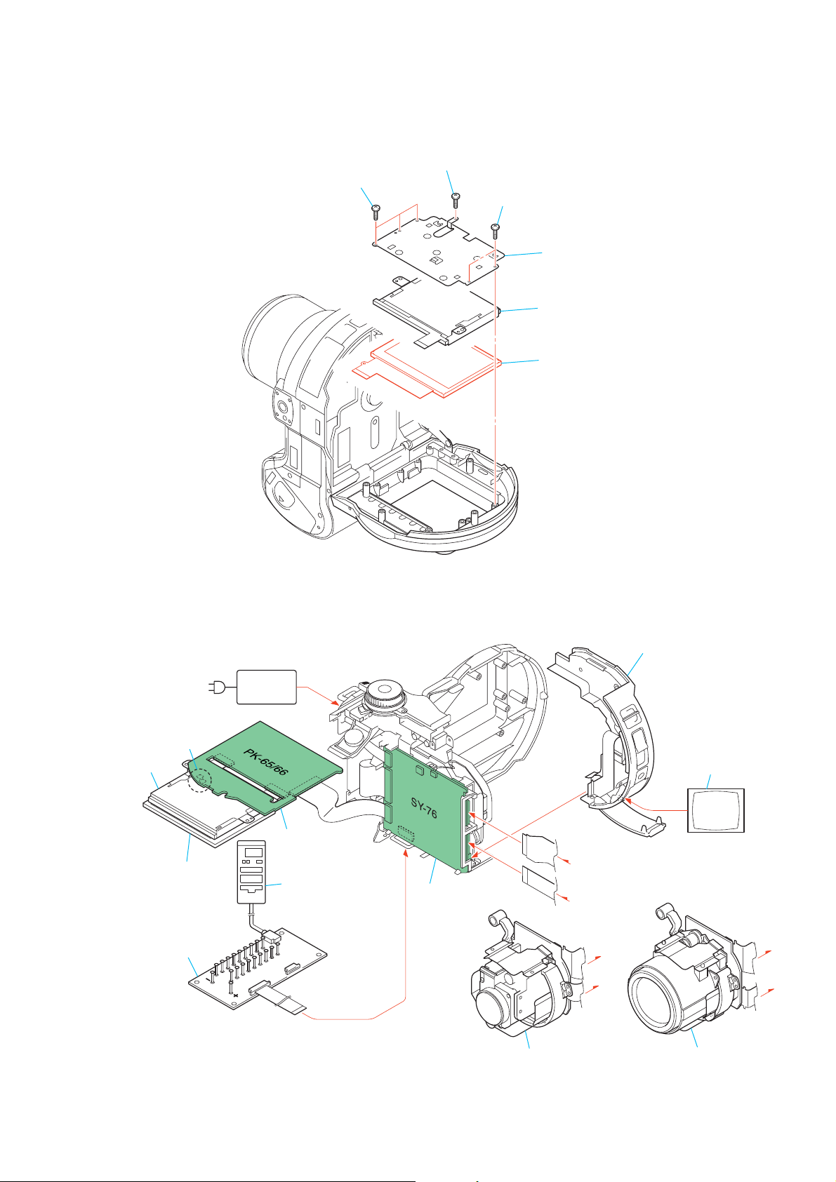
2 Three screws
(M1.7
×
4)
1 Screw
(M1.7 × 5)
3 Two screws
(M1.7
×
4)
4 BL retainer
5 Back light unit
6 LCD module
MVC-CD250/CD400
[SERVICE POSITION (PK-65/66 BOARD: SIDE B)]
DC-IN
S307, S308
(Note 3)
Back light unit
LCD module
CPC-9 jig
(J-6082-393-C)
(Note 1, 2)
AC power
adaptor
PK-65/66 board
18
1
Adjustment remote
commander
18
1
SY-76 board
A
B
Side cabinet block assembly
A
B
Monitor
A
B
Note 1: Don’t use the 12 pin flexible board of CPC-9 jig.
It causes damage to the unit.
Note 2: The old CPC-9 jig (Parts code: J-6082-393-B) Cannot be used,
because it cannot operate the adjustment remote commander.
Note 3: Must be pressed lid open/close detect switch (S307, S308 on
PK-65/66 board) when using the CD-R/RW drive unit.
2-9
Lens block assembly
(MVC-CD250)
Lens block assembly
(MVC-CD400)
MVC-CD250/CD400
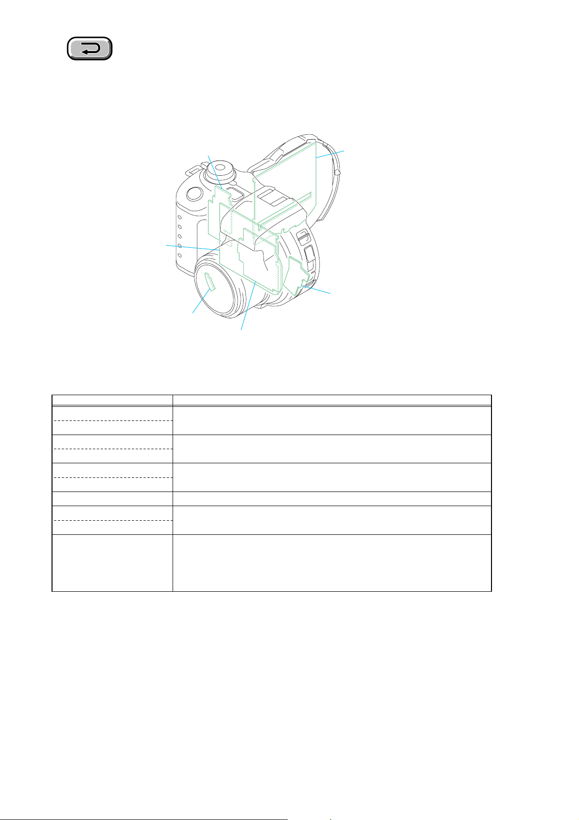
2-12.CIRCUIT BOARDS LOCATION
FS-84 (MVC-CD400)
FS-85 (MVC-CD250)
SY-76
LS-61 (MVC-CD400)
PK-65 (MVC-CD400)
PK-66 (MVC-CD250)
JK-224 (MVC-CD400)
JK-225 (MVC-CD250)
CD-393 (MVC-CD400)
CD-394 (MVC-CD250)
Board Name Function
CD-393 (MVC-CD400) CCD IMAGER, CAMERA PROCESS
CD-394 (MVC-CD250)
FS-84 (MVC-CD400) DC IN, CONTROL SW
FS-85 (MVC-CD250)
JK-224 (MVC-CD400) JACK
JK-225 (MVC-CD250)
LS-61 (MVC-CD400) LENS CAP SWITCH
PK-65 (MVC-CD400) LCD DRIVE, TIMING GENERATOR, BACK LIGHT DRIVE
PK-66 (MVC-CD250)
SY-76 CAMERA DSP, VIDEO, MEMORY, LENS DRIVE, SH DSP,
CD-R/RW SIGNAL PROCESS, CD DRIVE, CD DRIVE DSP,
AUDIO, LASER/IR LED DRIVE, HI CONTROL,
DC/DC CONVERTER
2-10
2-10E
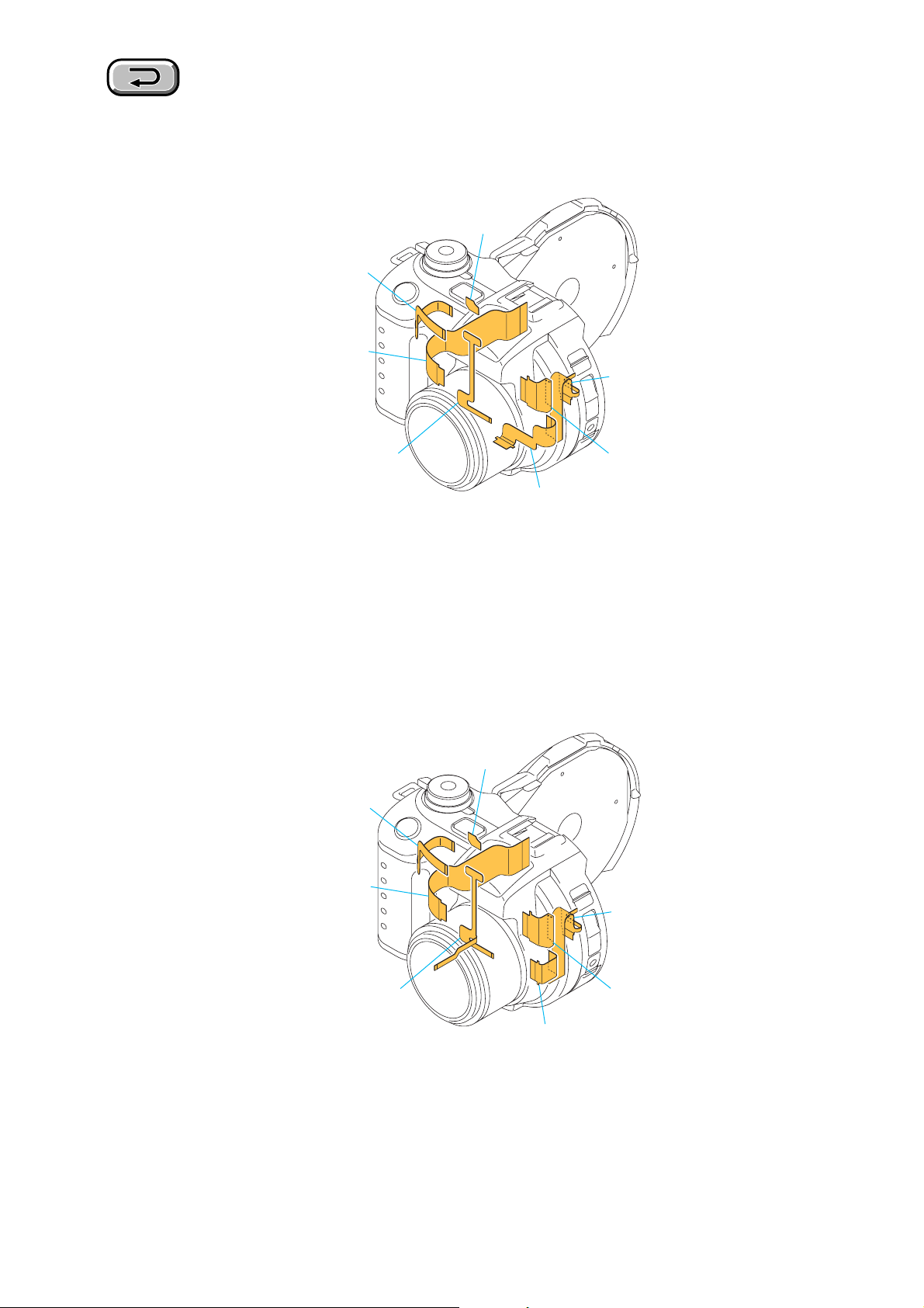
2-13.FLEXIBLE BOARDS LOCATION
(MVC-CD250)
FP-481
FP-483
MVC-CD250/CD400
FP-248
FP-482
(MVC-CD400)
FP-481
FP-483
FP-489
FP-484
FP-486
FP-248
FP-482
FP-490
FP-484
FP-485
2-11E

COVER
COVER
Link
Link
MVC-CD250/CD400
3. BLOCK DIAGRAMS
OVERALL BLOCK DIAGRAM
OVERALL BLOCK DIAGRAM
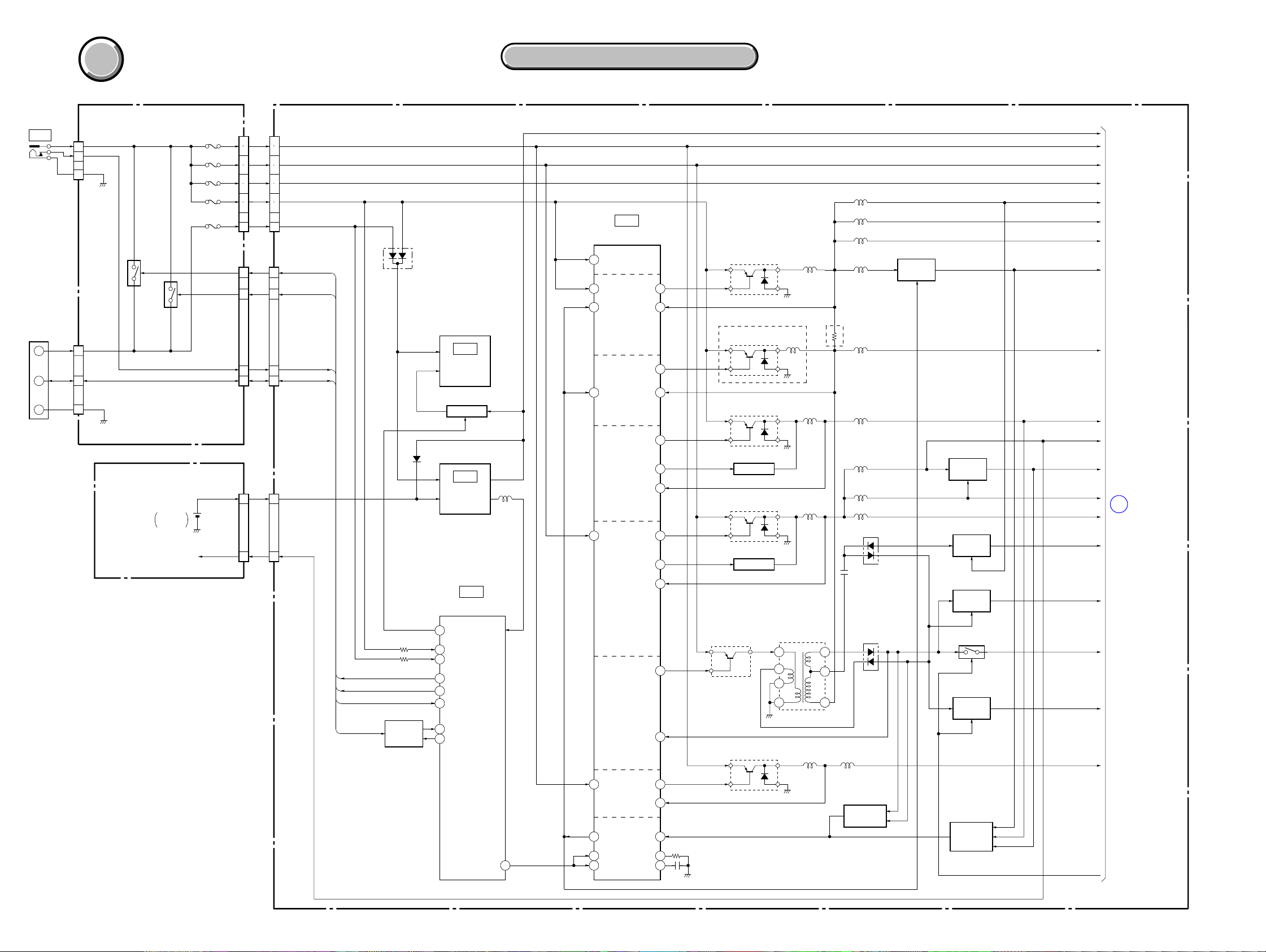
POWER BLOCK DIAGRAM-1
POWER BLOCK DIAGRAM-1
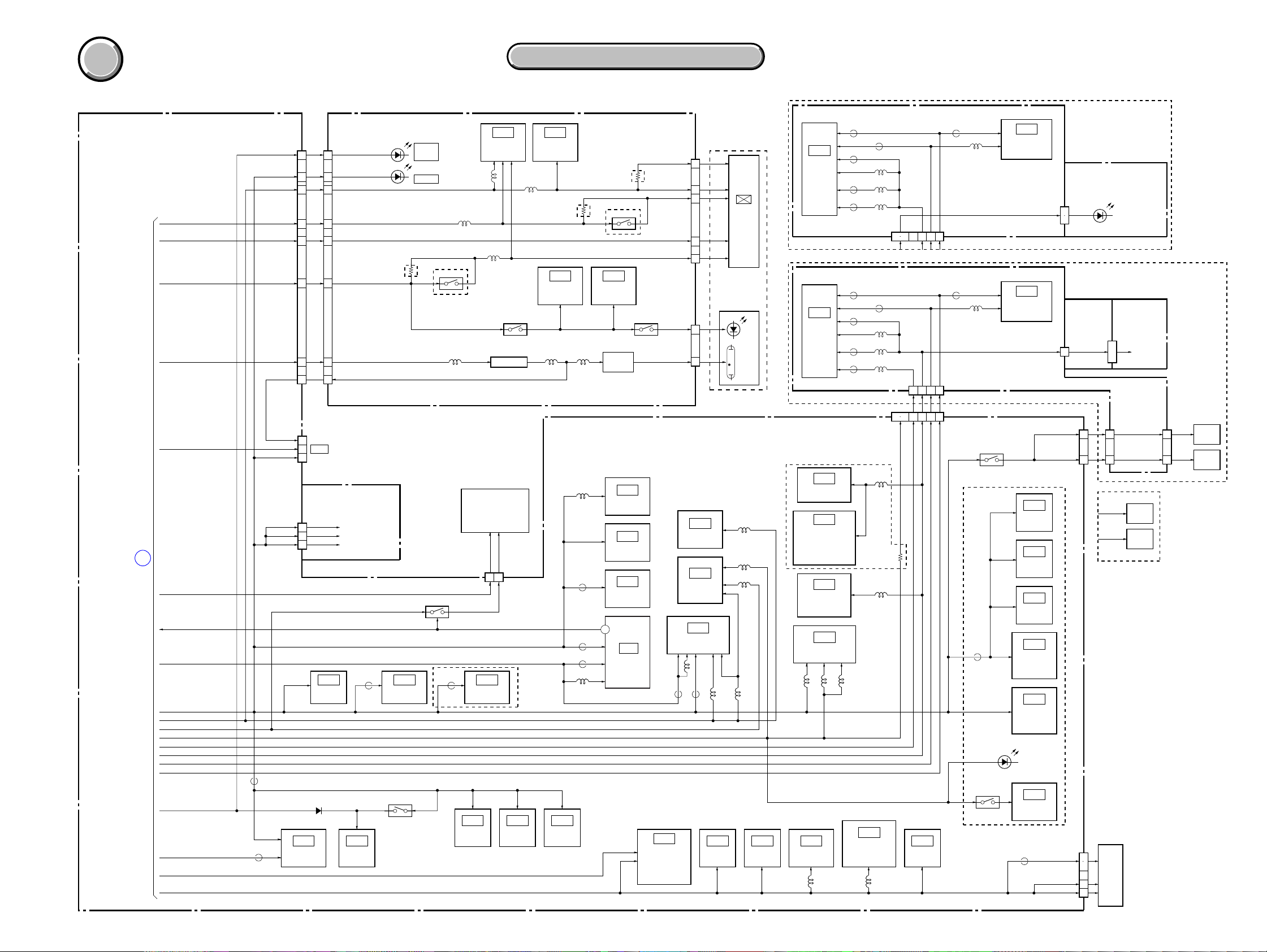
POWER BLOCK DIAGRAM-2
POWER BLOCK DIAGRAM-2
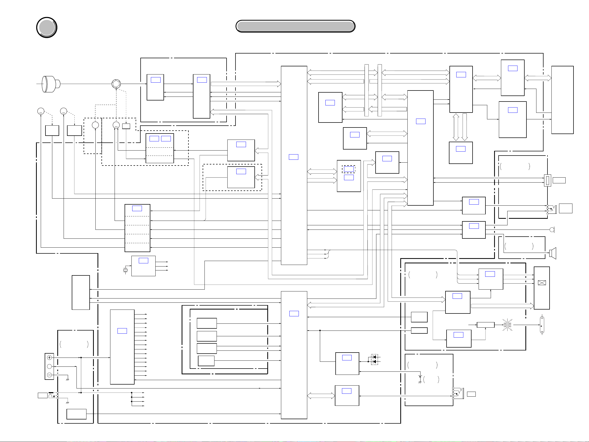
MVC-CD250/CD400
COVER
COVER
3-1. OVERALL BLOCK DIAGRAM
FOCUS
MOTOR
J9001
DC IN
LENS
FOCUS
SENSOR
BT9001
BATTERY
TERMINAL
S
05
ZOOM
MOTOR
MM
ZOOM
SENSOR
FLASH
UNIT
FS-84/85 BOARD
(1/2)
FS-84:MVC-CD400/
FS-85:MVC-CD250
BATT SIG
FUNCTION
KEY
CD400
IRIS
METER
(SHUTTER)
IRIS
METER
STRB ON
STB CHARGE
XSTB FULL
IRIS
MM
X601
CONTROL
(13/13)
H
SHUTTER DRIVE
IC001
DC
DRIVE−
HALL+
IC101
(3/13)
IRIS
IRIS MOTOR
DRIVE
ZOOM MOTOR
DRIVE
FOCUS MOTOR
DRIVE
SECTION 3
3. BLOCK DIAGRAMS
3. BLOCK DIAGRAMS
BLOCK DIAGRAMS
( ) : Number in parenthesis ( ) indicates the division number of schematic diagram where the component is located.
CD-393/394 BOARD
(CD-393:MVC-CD400/CD-394:MVC-CD250)
IC401
CCD OUT
CCD
IC601
CLOCK GEN.
(5/13)
MT UNREG
BL UNREG
ST UNREG
BATT UNREG
IMAGER
(1/2)
IC102 IC106
IRIS DRIVE
HALL AMP
Z SENS RST
F SENS RST
D 1.5V
D 2.5V
D 3.1V
A 3.1V
A 4.9V
4.6V
M 4.6V
PANEL 4.9V
PANEL 13.5V
PANEL –15.3V
CAM 5V
CAM P 5V
CAM 3.1V
CAM 15V
CAM −7.5V
(3/13)
H1, H2
V1A, V1B, V2, V3A,
V3B, V4, VSHT, RG
HALL AD
TG CLK
MC CLK1
USB CLK
IC501
CAMERA
MODULE
(2/2)
CD250
CD400
HALL AD
CONTROL SWITCH BLOCK
ZOOM
SWITCH
SHUTTER
SWITCH
MODE
DIAL
POWER
ON/OFF
CAM SO, XCAM SCK
DIR0A, DIR0B
XPWR ON
SY-76 BOARD
DATA BUS 14
CA HD
CA FD
MCK12
IC108
EVR
(D/A CONVERTER)
(3/13)
IC105
IRIS CONTROL
(3/13)
MSHUT EN, MSHUT ON
IRIS EN
HR EN1,
HR DIR1A, HR DIR1B
HR EN0,
HR DIR1A, HR DIR0B
STRB ON
STB CHARGE
XSTB FULL
KEY AD 3
XSHTR ON, XAE LOCK SW
MODE DIAL
XPB ON
KEY AD 0, 1
CAM SI, CAM SO, XCAM SCK
SYS DD ON
BATT SIG
IC301
CAMERA
DSP
(1/13)
CAM SI, CAM SO, XCAM SCK
IC402
HI
CONTROL
(12/13)
DATA BUS 32
ADDRESS BUS 14
CV OUT
AU AINL AU AINL
AU AOUT AU AOUT
PANEL R
PANEL G
PANEL B
BEEP, BEEP ON
FR SO, FR SI, XFR SCK
KEY AD2
LANC DATA
16
25
32M FLASH
IC503
(5/13)
16
21
IC805
EEPROM
(9/13)
CD400
IC302
IC303
128M SDRAM
(2/13)
FR XRESET
IC403
INITIAL RESET,
BACK UP VCC
(12/13)
IC401
LANC DRIVER
(12/13)
DATA BUS
ADDERESS BUS
CDC SI, CDC SO, CDC SCK
EEPROM
CAM SI, CAM SO, XCAM SCK
D403
UNREG
UNREG
16
25
IC504
(5/13)
HALL AD
LCD SO, LCD SCK
FR SO, FR SI, XFR SCK
BATT
ACV
16
16
MC XRD
MC XWE1
IC501
MC CAM,
SH DSP
(4/13)
USB D+ D+
USB D– D–
VAMP ON
BEEP, BEEO ON
PK-65/66 BOARD
PK-65:MVC-CD400/
PK-66:MVC-CD250
LCD SO, LCD SCK
FUNCTION
KEY
RESET
BL LEV
JK-224/225 BOARD (2/2)
JK-224:MVC-CD400/
JK-225:MVC-CD250
BT101
LITHIUM
BATTERY
LANC SIG
IC807
CD DRIVVE
DSP
(8/13)
DATA BUS 16
IC803
SRAM
(9/13)
CV OUT
PANEL R
PANEL G
PANEL B
IC302
TIMING
GENERATOR
(1/2)
BL UNREG
IC201
DC/DC CONTROL
(2/2)
CD-R/RW DATA
ADDRESS BUS 17
IC201
VIDEO AMP
(2/13)
IC251
AUDIO DSP
(10/13)
Q206
SWITCHING
J101
ACC
IC905
CD-R/RW
SIGNAL
PROCESS
(6/13)
IC904
TRACKING/FOCUS/
SLED MOTOR/
SPINDLE MOTOR
DRIVE
(7/13)
JK-224/225 BOARD (1/2)
JK-224:MVC-CD400/
JK-225:MVC-CD250
AU OUT
FS-84/85 BOARD (2/2)
FS-84:MVC-CD400/
FS-85:MVC-CD250
IC301
LCD
DRIVE
(1/2)
T201
INVERTER
TRANS
V OUT
VR
VG
VB
BL HIGH
CD-R/RW DATA
LCD9001
COLOR
LCD
MONITOR
ND9001
BASE UNIT
(DDX-G3000)
CN102
USB
J102
A/V OUT
(MONO)
MIC9001
MICROPHONE
SP9001
SPEAKER
3-1 3-2
MVC-CD250/CD400
COVER
COVER
3. BLOCK DIAGRAMS
3. BLOCK DIAGRAMS
3-10.POWER BLOCK DIAGRAM 1
FS-84/85 BOARD
J9001
DC IN
BT9001
BATTERY
TERMINAL
+
S
–
(FS-84:MVC-CD400/FS-85:MVC-CD250)
CN002
ACV UNREG
1
BATT/XEXT
3
ACV GND
2
Q001, 002
Q003, 004
CN003
1
2
3
BATT
UNREG
BATT SIG
BATT GND
CHARGE
CONTROL
CN004
F001
F002
F004
F003
F005
CN005 CN721
( ) : Number in parenthesis ( ) indicates the division number of schematic diagram where the component is located.
SY-76 BOARD (1/2)
IC001
DC CONTROL
(13/13)
EVER 3.2V
MT UNREG
BL UNREG
ST UNREG
ACV UNREG
OUT-6
IN(C)6
OUT-5
IN(C)5
4
9
64
1415 +IN(E)5
6
7
8
9
12
13
10
11
14
8
9
7
5
CN001
8
M 4.6V
9
TRANS/3.1V
6
7
ST UNREG
2
3
5V
5
4
BATT UNREG
1
FAST CHARGE
8
9
7
5
INIT CHARGE
BATT/XEXT
BATT SIG
D403
IC401
LANC DRIVER
(12/13)
Q401
SWITCHING
28
VCC
63 VCC4, 5, 6
10
+IN(E)6
CD400
Q004
SWITCHING
Q005
SWITCHING
Q001
SWITCHING
L002
L001
CD250
L009
L010
L011
L012
L013
L014L004
Q020 - 022
4.6V
REG
EVER
MT UNREG
BL UNREG
ST UNREG
PANEL 4.9V
CAM 5V
A 4.9V
4.6V
CAM P 5V
D 1.5V
JK-224/225 BOARD
(JK-224:MVC-CD400/JK-225:MVC-CD250)
BT101
LITHIUM
BATTERY
D 3.1V
CN103 CN718
21 1
12 8
VL 3V
D 3.1V
FAST CHARGE
INIT CHARGE
BATT/EXT
BATT SIG
Q408
BATTERY
CHARGE
DETECTOR
D407
IC403
INITIAL RESET,
BACK UP VCC
(12/13)
IC402
HI CONTROL
(12/13)
18 XLANC ON
68
ACV SENS
67 BATT SENS
48
FAST CHARGE
47
INIT CHARGE
8
BATT/XEXT
43
BATT SI
42
BATT SO
L401
42 VCC1, 3
OUT-4
MOS-GATE-4
OUT-1
MOS-GATE-1
OUT-3
IN(C)3
57
Q009, 011
2.5V
REG
Q014, 017
–15.3V
REG
Q013, 016
13.5V
REG
Q018, 019
Q012, 015,
024, 025
–7.5V
REG
60
18IN(C)4
46
43
40IN(C)1
56
34
SWITCHING
SWITCHING
Q003
SWITCHING
Q007
Q002
SWITCHING
Q008
Q006
SWITCHING
T001
DC/DC CONV.
TRANS
4
3
2
1
L003
L005 L015
L008
L007
L006
D001
RECT
D003
RECT
5
6
8
D 3.1V
D 2.5V
A 3.1V
CAM 3.1V
PANEL –15.3V
PANEL 13.5V
CAM 15V
CAM –7.5V
M 4.6V
A
(PAGE 3-21)
POWER 2
SCP
50OUT-2
37IN(C)2
13
21
RT
2276SYS DD ON
CT
EMERGENCY
51 VCC2
27
V REF
29
CTL2
30
CTL1
05
3-19 3-20
Q023
DETECT
VREF
D 3.1V
Q010
EMERGENCY
DETECT
CAM DD ON
COVER
COVER
3. BLOCK DIAGRAMS
3. BLOCK DIAGRAMS
MVC-CD250/CD400
3-11.POWER BLOCK DIAGRAM 2
SY-76 BOARD (2/2)
CN717
EVER
D 3.1V
A 3.1V
PANEL 13.5V
PANEL –15.3V
PANEL 4.9V
BL UNREG
CN714
BL DC
MT UNREGMT UNREG
D 3.1V
CN720
D 3.1V
D 3.1V
D 3.1V
POWER 1
(PAGE 3-20)
05
A
EVER
A 3.1V
D 3.1V
ST UNREG
CAM DD ON
D 1.5V D 1.5V
D 3.1V
A 3.1V
A 4.9V
CAM P 5V
CAM 5V
CAM 3.1V
CAM 15V
CAM –7.5V
FB801
EVER
D 2.5V
4.6V
M 4.6V
FB802
( ) : Number in parenthesis ( ) indicates the division number of schematic diagram where the component is located.
PK-65/66 BOARD
(PK-65:MVC-CD400/PK-66:MVC-CD250)
CN303
EVER
3
3
D 3.1V
27
27
14
12
11
13
10
4
13
10
18
9
14
16
IC807
CD DRIVE DSP
(8/13)
PANEL 3.1V
14
PANEL 13.5V
12
PANEL –15.3V
11
PANEL 4.9V
13
BL UNREG
10
BL DC
4
CPC
CONTROL SWITCH BLOCK
IC906
AND
(6/13)
D801
(ZK-880)
(ZK-860)
D 3.1V
D 3.1V
D 3.1V
FB303
D 3.1V
IC803
SRAM
(9/13)
: CD400
: CD250
CD250
IC302
128M SDRAM
(2/13)
Q801
D303
FLASH
/CHG
D302
ACCESS
Q701, 702
CD400
Q304
FB304
L201
L303
CN719
128M SDRAM
IC805
EEPROM
(9/13)
L301
IC303
(2/13)
IC301
LCD DRIVE
(1/2)
L304
Q203, 206
SWITCHING
FLASH
UNIT
A 4.9V
UNREG
24
IC804
AND
(9/13)
L302
CD400
IC302
TIMING
GENERATOR
(1/2)
CURRENT
DETECT
D 3.1V
D 3.1V
A 3.1V
A 4.9V
CAM P 5V
CAM 5V
CAM 3.1V
CAM 15V
CAM –7.5V
IC202
(2/2)
IC806
AND
(9/13)
CD250
L203L202
L601
FB504
FB501
FB502
L501
CD250
CD400
Q307
IC201
DC/DC
CONTROL
(2/2)
T201
INVERTER
TRANS
CLOCK GEN.
EEPROM
32M FLASH
198
PTM(6)
MC CAM,
IC601
(5/13)
IC504
(5/13)
IC503
(5/13)
IC501
SH DSP
(4/13)
CN302
VDD/VGLAC
VDD/VSH3V
VGH
VGL
VDD/VSH5V
Q210Q201, 202
CN201
LED
BL HIGH
L301
FB302
IC904
TRACKING/FOCUS/
SLED MOTOR/
SPINDLE MOTOR
DRIVE
(7/13)
Note : CN302 Pin name A/B
4
23
1
3
24
2
10
IC201
VIDEO AMP
(2/13)
IC251
AUDIO DSP
(10/13)
IC301
CAMERA DSP
(1/13)
FB301 L302
SWITCH
A : CD250
B : CD400
PANEL UNIT
MONITOR
ND9001
L252
IC911
(6/13)
LCD9001
COLOR
LCD
LED
BACK
LIGHT
L201
L253
L251
IC912
SWITCH
(7/13)
CD-394 BOARD
IC501
CAMERA
MODULE
(2/2)
CD-393 BOARD
IC501
CAMERA
MODULE
(2/2)
Note : CN724 Pin name A/B
A : CD400
B : CD250
CD250
IC102
IRIS DRIVE
(3/13)
IC106
IRIS DRIVE
HALL AMP
HALL BAIS CONTROL
HALL GAIN CONTROL
(3/13)
IC108
EVR
(D/A CONVERTER)
(3/13)
IC101
7CH LENS DRIVER
(3/13)
L102 L104 L105
IC903
COMPARATOR
(6/13)
L902
FB505 FB401
FB504
FB503
L502
L501FB501
L503FB502
CN503
48 49
FB505 FB401
FB504
FB503
L502
L501FB501
L503FB502
CN501
48 49
CN724
LD OUT/CAM P 5V
L101
L103
D 3.1V
CAM P 5V
CAM P 5V
IC905
CD-R/RW
SIGNAL PROCESS
(6/13)
L901
43
CAM 5V
IC901
AND
(6/13)
CAM 15V
CAM 3.1VCAM 3.1V
404442
40404444424243
CAM –7.5V
D 3.1V
L401
L401
CD400
FB101
Q101
Q151, 152
IC401
CCD
IMAGER
(1/2)
CN502
CAM P 5V
IC401
CCD
IMAGER
(1/2)
CN502
CAM 3.1V
F SENS VCC
Z SENS VCC
IC103
XOR
(3/13)
IC104
XOR
(3/13)
IC107
D-FF
(3/13)
IC105
IRIS
CONTROL
(3/13)
IC151
MULTI
VIBRATOR
(11/13)
D302
(SELF TIMER)
IC152
COMPARATOR
(11/13)
FB901
FP-489 FLEXIBLE BOARD
1
2
FP-490
FLEXIBLE
BOARD
5
CN651 CN703
20
20
7
7
BASE UNIT
(DDX-G3000)
CN901
LDVCC
11
12
FPDO
15
PDVCC
17
D9002
(AF/SELF TIMER)
LS-61
BOARD
CN801
1
CAM 3.1V
ı
3
F SENS VCC
Z SENS VCC
FOCUS
SENSOR
ZOOM
SENSOR
CN701
CD250
CD250
CD400
FOCUS
14
SENSOR
ZOOM
2
SENSOR
3-21 3-22E
COVER
COVER
PRINTED WIRING BOARDS AND SCHEMATIC DIAGRAMS
4-1. FRAME SCHEMATIC DIAGRAMS
SECTION 4
4-2. SCHEMATIC DIAGRAMS 4-3. PRINTED WIRING BOARDS
4-2. SCHEMATIC DIAGRAMS 4-3. PRINTED WIRING BOARDS
MVC-CD250/CD400
1
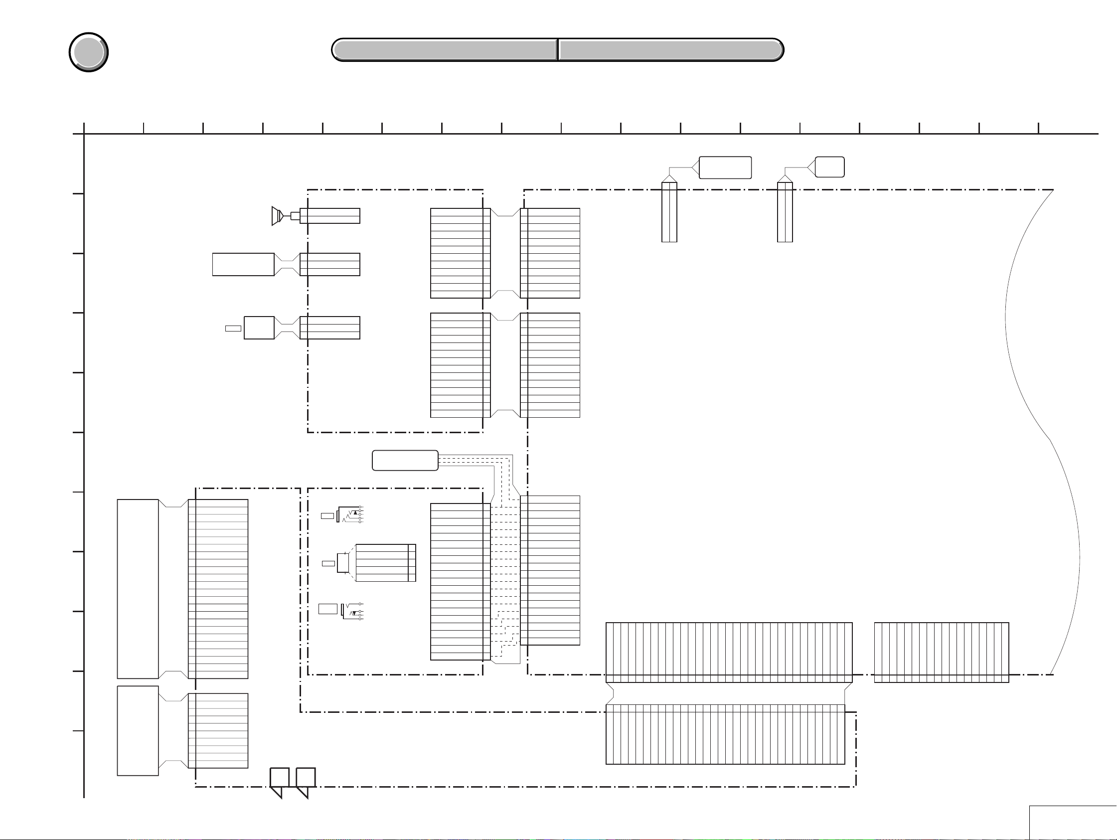
FRAME SCHEMATIC DIAGRAM (1/2)
A
B
C
D
E
3
SP9001
BT9001
BATTERY TERMINAL
J9001
DC IN
DC JACK
CN006
SP-
2
SP+
1
3BATT_GND
2BATT_SIG
1BATT_UNREG
3BATT/XEXT
2 ACV_GND
1 ACV_UNREG
FS-84 BOARD
:CD400
FS-85 BOARD
:CD250
5
2P
3PCN003
3PCN002
684 172
CN005
REG_GND
REG_GND
BATT_SIG
REG_GND
BATT/XEXT
FAST_CHARGE
INIT_CHARGE
REG_GND
KEY_AD0
KEY_AD1
CN004
REG_GND
REG_GND
REG_GND
REG_GND
REG_GND
M_4.6V
M_4.6V
TRANS/3.1V
TRANS/3.1V
ST_UNREG
ST_UNREG
BATT_UNREG
7
12P
1
SP+
2
SP-
3
4
5
6
7
8
9
10
11
12
14P
1
2
3
4
5
6
7
8
9
10
5V
5V
11
12
13
14
FS-141 HARNESS FP-481 FLEXIBLE
1
2
3
4
5
6
7
8
9
10
11
12
14
13
12
11
10
9
8
7
6
5
4
3
2
1
SP+
SP-
REG_GND
REG_GND
BATT_SIG
REG_GND
BATT/XEXT
FAST_CHARGE
INIT_CHARGE
REG_GND
KEY_AD0
KEY_AD1
CN001
REG_GND
REG_GND
REG_GND
REG_GND
REG_GND
M_4.6V
M_4.6V
TRANS/3.1V
TRANS/3.1V
5V
5V
ST_UNREG
ST_UNREG
BATT_UNREG
12PCN721
14P
91411 12 16
DS-116
HARNESS
1
2PCN707
DEW_SENS
2
REG_GND
FP-248 FLEXIBLE
DEW SENSOR
2P
CN702
1
MIC_SIG
2
MIC_GND
13
MIC9001
MIC
1510
SY-76 BOARD (1/2)
CONTINUED ON
PAGE 4-3
PL9001
4
1
5
2
3
J102
DOOR LOCK
CN102
5P
VCC
1
D-
2
D+
3
4
ID
5
GND
PK-65 BOARD
PK-66 BOARD
CN103
EXT_STROB_ON
XLANC_JACK_IN
XUSB_JACK_IN
AV_JACK_IN
:CD400
:CD250
REG_GND
LANC_SIG
REG_GND
LANC_DC
USB_GND
USB_D+
USB_D-
REG_GND
D_3.1V
REG_GND
REG_GND
AU_OUT
REG_GND
V_OUT
REG_GND
REG_GND
VL_3V
21P
1
2
3
4
5
6
7
8
9
10
11
12
13
14
15
16
17
18
19
20
21
FP-482
FLEXIBLE
21pin - 20pin
20
19
18
17
16
15
14
13
12
11
10
9
8
7
6
5
4
3
2
1
DOORLOCK
REG_GND
LANC_SIG
REG_GND
LANC_DC
EXT_STROB_ON
XLANC_JACK_IN
USB_GND
USB_D+
USB_D-
REG_GND
XUSB_JACK_IN
D_3.1V
AV_JACK_IN
REG_GND
AU_OUT
REG_GND
V_OUT
REG_GND
VL_3V
20PCN718
33PCN717
XLID_OPEN
BL_DC
VG
EVER
3EVER
4BL_DC
HSY
5VG
6HSY
CHARGE_LED
123456789
1XLID_OPEN
2CHARGE_LED
32P
CN303
PANEL_COM
BL_GND
BL_GND
PANEL_3.1V
PANEL_4.9V
PANEL_13.5V
REG_GND
PANEL_-15.3V
BL_UNREG
1011121314151617181920212223242526272829303132
PANEL_B
PANEL_G
PANEL_R
REG_GND
REG_GND
XHD
XSYS_RST
LCD_SO
LCD_SCK
XVD
FP-483 FLEXIBLE
7PANEL_COM
8BL_GND
9BL_GND
10BL_UNREG
11PANEL-15.3V
12PANEL_13.5V
13PANEL_4.9V
14PANEL_3.1V
15REG_GND
16PANEL_B
17PANEL_G
18PANEL_R
19REG_GND
20REG_GND
21XSYS_RST
22XHD
23XVD
24LCD_SO
25LCD_SCK
XCS_LCD
26XCS_LCD
D_3.1V
27D_3.1V
KEY_AD2
28KEY_AD2
REG_GND
29REG_GND
FR_XRESET
REG_GND
30FR_XRESET
31REG_GND
ACCESS_LED
32ACCESS_LED
18P
CN714
DECEFM
MPXO
N.C
33
FMDT
123456789
REG_GND
XLID_OPEN
N,C
HSY
PANEL_COM
(FOR CHECK)
LANC_OUT
LANC_IN
BL_DC
MS_SCLK
MS_BS
VG
MT_UNREG
101112131415161718
CPC
MS_DIO
D_3.1V
N.C
F
24PCN302
VDD/VSH5V
24
23
VDD/VSH3V
22
G
H
LCD9001
PANEL UNIT
I
J
ND9001
BACK LIGHT
K
VSS/GND
21
VB
VG
20
19
VR
18
HCNT/SPD
17
MCLK/CLD
16
CLR/CTR
15
OE/PSS2
14
SRT/PSS1
13
STBYB/RES
12
VBC/CLS
11
VCOM
10
RESET/EX2
9
STBYB/PSG
8
GSRT/MO2
7
GPCK/MO1
6
GRES/EX1
5
N.C./SPS
4
VDD/VGLAC
3
VGL
2
VSS/GND
1
VGH
10PCN201
BL_HIGH
10
N.C.
9
N.C.
8
N.C.
7
N.C.
6
N.C.
5
N.C.
4
BL_LOW
3
LED
2
LED_GND
1
Note:CN302 Pin
Name A/B
A:CD250
B:CD400
J101
ACC
STROB JACK
USB
A/V OUT
(MONO)
AV JACK
JK-224 BOARD
:CD400
JK-225 BOARD
:CD250
05
4-1 4-2
FRAME (1/2)
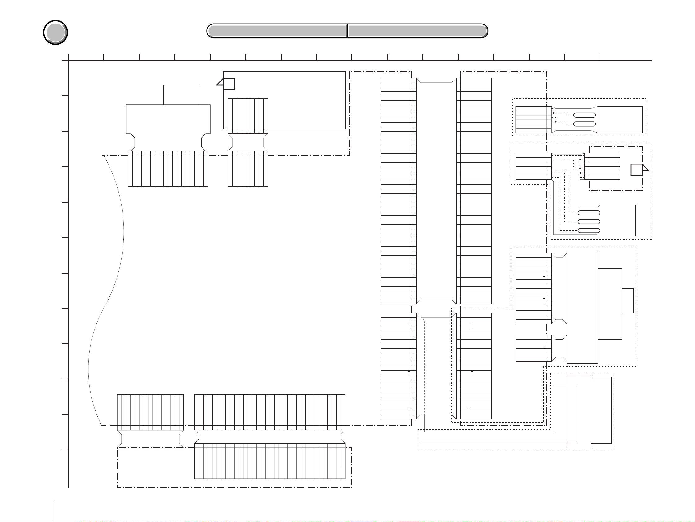
MVC-CD250/CD400
COVER
COVER
4-2. SCHEMATIC DIAGRAMS 4-3. PRINTED WIRING BOARDS
4-2. SCHEMATIC DIAGRAMS 4-3. PRINTED WIRING BOARDS
1
FRAME SCHEMATIC DIAGRAM (2/2)
A
B
C
123456789
18P
XSHTR_ON
CN720
D
E
F
CONTINUED ON
PAGE 4-2
G
H
I
J
15PCN902
1 SLED+
2 SLED-
3 VH-
K
L
05
3
CONTROL SWITCH
BLOCK
(ZK-880):CD400
N.C
N.C
XPB_ON
XSET_UP
MODE_DIAL
XPOWER_ON
XAE_LOCK_SW
4W-
5W+
6V+
7V-
8U+
9U-
10 VH+
BASE
UNIT
(DDX-G3000)
:CD250(ZK-860)
101112131415161718
N.C
N.C
GND
11 XLMT
D_3.1V
12 LEDGND
D_3.1V
KEY_AD3
13 U
14 V
15 W
D_3.1V
XPOWER_LED
34P
CN901
1
34P
FCS+
5
DIAL_A
DIAL_B
SY-76 BOARD (2/2)
TRK-32TRK+33FCS-34FCS+
28 D
29 G
30 - (OP_TEMP)
31
2
3
4
5
6G7D8C9
FCS-
TRK-
TRK+
- (OP_TEMP)
UNREG
A_4.9V
UNREG_GND
HARNESS
A_4.9V
UNREG_GND
25 RFSUM
10
RFSUM
SS-084
UNREG
24 SW
11SW12
PDGND
XSTB_FULL
STROB_ON
STROB_ON
XSTB_FULL
PDVC23PDGND
22
13
PDVC
STB_CHARGE
123456789
123456789
9P
CN719
STB_CHARGE
26E27 C
E
6842
PLUNGER_ON
EXT2_STRB_ON
XSTB_POPUP
XSTB_POPUP
PLUNGER_ON
EXT2_STRB_ON
19 A
20B21 F
FP-488 FLEXIBLE
14F15B16A17H18
PDVCC
FLEXIBLE
FP-490
FP-489
LND001
LND002
LENS
BLOCK
1510
6
XLENSCAP_ON
5
XLENSCAP_ON
4
XLENSCAP_ON
3
CAM_3.1V
2
CAM_3.1V
1
CAM_3.1V
LS-061 BOARD
LND003
LND002
LND001
LENS BLOCK
CD250
D9002
AF/
SELF TIMER
ILLUMINATOR
6PCN801
D9001
LASER
UNIT
CD400
CD250
7
FLASH
UNIT
MODAMP
13 FPDVC
VWDC110VRDC11LDVCC12LDVCC
8 VWDC2
9
FPDGND
FPDVCC16FPDO17PDVCC18H
14
15
ENBL3OSCEN4WE25WE16LDGND7LDGND
1
2
91411 12 16
CN724
CD_GND
CA_AD10
CA_AD11
CA_AD12
CA_AD13
CD_GND
CD_GND
CD_GND
CD_GND
CD_GND
CD_GND
XGCAM_CS
CAM_SO
XCAM_SCK
TG_WEN
XCAM_RESET
VSUB_CONT
CD_GND
CD_GND
CCD_TEMP
CD_GND
CD_GND
CAM_-7.5V
REG_GND
CAM_3.1V
CAM_5V
CAM_15V
XLENSCAP_ON
PD_OUT/PRELAMP_LED
PD_OUT/PRELAMP_LED
LD_OUT/CAM_P_5V
LD_OUT/CAM_P_5V
CN651
ZOOM_B
ZOOM_A
ZOOM_B
ZOOM_A
Z_SENS_GND
Z_SENS_RST
Z_SENS_VCC
FOCUS_B
FOCUS_A
FOCUS_B
FOCUS_A
F_SENS_GND
F_SENS_RST
F_SENS_VCC
CA_AD0
CA_AD1
CA_AD2
CA_AD3
CA_AD4
CA_AD5
CA_AD6
CA_AD7
CA_AD8
CA_AD9
TG_CLK
MCK12
XTG_CS
CLPDM
CLPOB
CA_FD
CA_HD
BIAS+
HALL+
BIAS-
HALL-
DRIVE+
DRIVE-
IRIS-B
IRIS-A
IRIS-B
IRIS-A
51P
1
2
3
4
5
6
7
8
9
10
11
12
13
14
15
16
17
18
19
20
21
22
23
24
25
FP-484
26
FLEXIBLE
27
28
29
30
31
32
33
34
35
36
37
38
39
40
41
42
43
44
45
46
47
Note:CN724,CN503
Pin Name A/B
48
A:CD400
B:CD250
49
50
N.C.
51
N.C.
24P
1
2
3
4
5
6
7
8
9
10
11
12
13
14
15
16
17
18
19
20
21
22
23
24
FP-485
FLEXIBLE
CN501:CD400
CN503:CD250
CD_GND
1
CA_AD0
2
CA_AD1
3
CA_AD2
4
CA_AD3
5
CA_AD4
6
CA_AD5
7
CA_AD6
8
CA_AD7
9
CA_AD8
10
CA_AD9
11
CA_AD10
12
CA_AD11
13
CA_AD12
14
CA_AD13
15
CD_GND
16
CD_GND
17
TG_CLK
18
CD_GND
19
CD_GND
20
MCK12
21
CD_GND
22
CD_GND
23
XGCAM_CS
24
CAM_SO
25
XCAM_SCK
26
XTG_CS
27
TG_WEN
28
CLPDM
29
CLPOB
30
CA_FD
31
CA_HD
32
XCAM_RESET
33
VSUB_CONT
34
CD_GND
35
CD_GND
36
CCD_TEMP
37
CD_GND
38
CD_GND
39
CAM_-7.5V
40
REG_GND
41
CAM_3.1V
42
CAM_5V
43
CAM_15V
44
XLENSCAP_ON
45
46
PD_OUT/PRELAMP_LED
PD_OUT/PRELAMP_LED
47
LD_OUT/CAM_P_5V
48
LD_OUT/CAM_P_5V
49
N.C.
50
N.C.
51
CN703
ZOOM_B
1
ZOOM_A
2
3
ZOOM_B
4
ZOOM_A
Z_SENS_GND
5
Z_SENS_RST
6
Z_SENS_VCC
7
BIAS+
8
HALL+
9
BIAS-
10
HALL-
11
DRIVE+
12
DRIVE-
13
FOCUS_B
14
FOCUS_A
15
FOCUS_B
16
FOCUS_A
17
F_SENS_GND
18
F_SENS_RST
19
F_SENS_VCC
20
IRIS-B
21
IRIS-A
22
IRIS-B
23
IRIS-A
24
51P
24P
24pin-20pin
19FPDO
20
21FPDGND
22
23
24LDVCC
25VRDC
26
27VWDC2
28LDGND
29LDGND
30
32
33
34
WE131WE2
FPDVCC
FPDVC
LDVCC
VWDC1
OSCEN
ENBL
MODAMP
13
CD-393 BOARD
:CD400
CD-394 BOARD
:CD250
CD400
TEMP_COM_(GND)
FP-486 FLEXIBLE
CN502
CAM_P_5V
CAM_P_5V
PRELAMP_LED
PRELAMP_LED
CN502
XLENSCAP_ON
CAM_3.1V
REG_GND
LD_OUT
PD_OUT
CN701
F_SENS_RST
F_SENS_VCC
F_SENS_GND
ZOOM_B
ZOOM_A
ZOOM_A
ZOOM_B
FOCUS_A
FOCUS_B
FOCUS_A
FOCUS_B
Z_SENS_RST
Z_SENS_VCC
Z_SENS_GND
CN702
IRIS-B
IRIS-A
IRIS-B
IRIS-A
6P
1
2
3
4
5
N,C
6
N,C
6P
FLEXIBLE
6
5
N,C
4
3
2
1
16P
16
N.C
15
14
13
12
11
10
9
8
7
6
5
4
3
2
1
6P
N.C
6
5
4
3
2
N.C
1
FRAME (2/2)
4-3 4-4
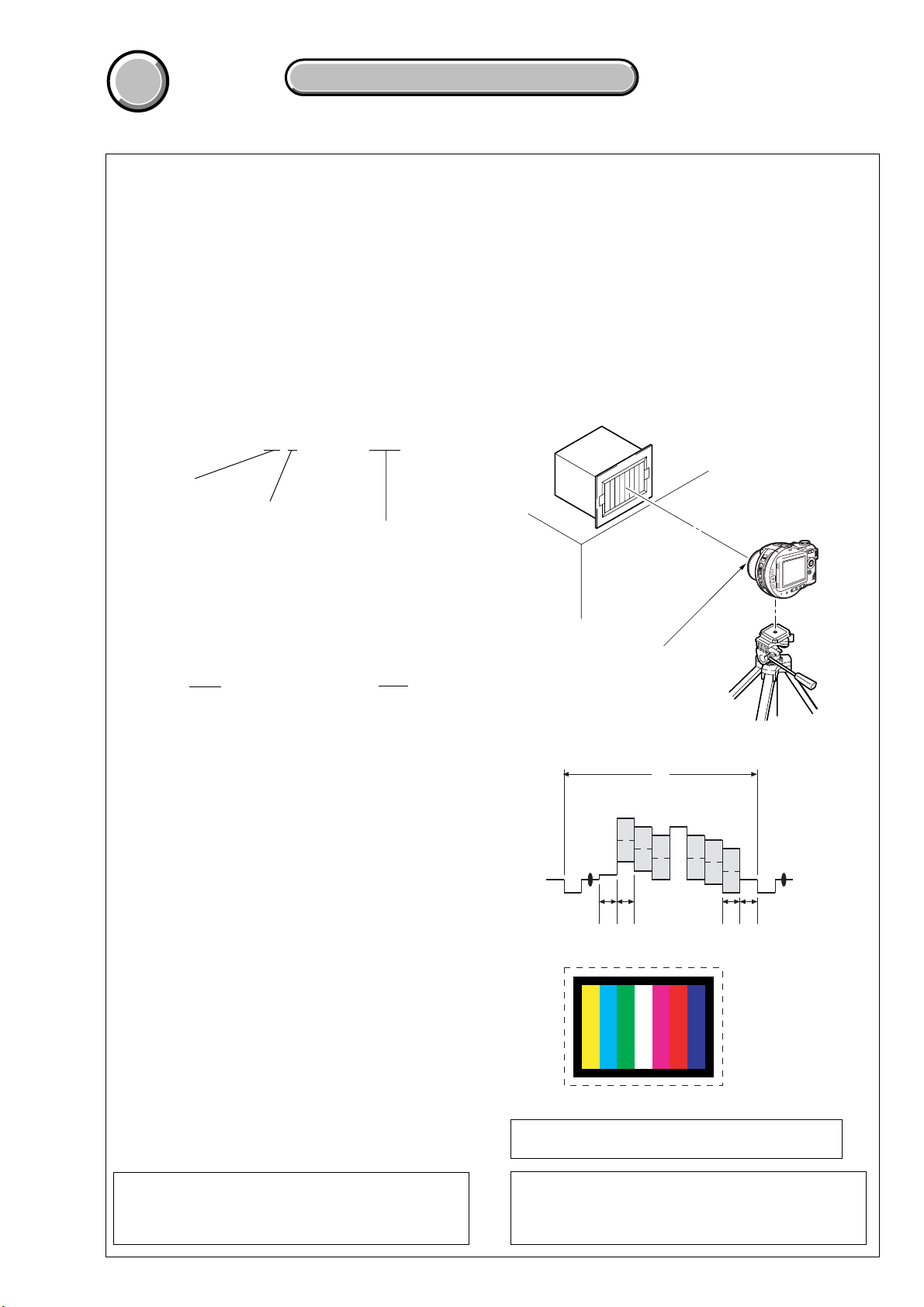
4-2. SCHEMATIC DIAGRAMS
COVER
COVER
4-2. SCHEMATIC DIGARAMS
4-2. SCHEMATIC DIAGRAMS
THIS NOTE IS COMMON FOR SCHEMATIC DIAGRAMS
(In addition to this, the necessary note is printed in each block)
MVC-CD250/CD400
(For schematic diagrams)
• All capacitors are in µF unless otherwise noted. pF : µ
µF. 50 V or less are not indicated except for electrolytics
and tantalums.
• Chip resistors are 1/10 W unless otherwise noted.
kΩ=1000 Ω, MΩ=1000 kΩ.
• Caution when replacing chip parts.
New parts must be attached after removal of chip.
Be careful not to heat the minus side of tantalum
capacitor, Because it is damaged by the heat.
• Some chip part will be indicated as follows.
Example C541 L452
22U 10UH
TA A 2520
Kinds of capacitor
Temperature characteristics
External dimensions (mm)
• Constants of resistors, capacitors, ICs and etc with XX
indicate that they are not used.
In such cases, the unused circuits may be indicated.
•Parts with ★ differ according to the model/destination.
Refer to the mount table for each function.
• All variable and adjustable resistors have characteristic
curve B, unless otherwise noted.
• Signal name
XEDIT→ EDIT PB/XREC → PB/REC
• 2: non flammable resistor
• 5: fusible resistor
• C: panel designation
• A: B+ Line
• B: B– Line
• J : IN/OUT direction of (+,–) B LINE.
• C: adjustment for repair.
• A: VIDEO SIGNAL (ANALOG)
• A: AUDIO SIGNAL (ANALOG)
• A: VIDEO/AUDIO SIGNAL
• A: VIDEO/AUDIO/SERVO SIGNAL
• A: SERVO SIGNAL
• Circled numbers refer to waveforms.
(Measuring conditions voltage and waveform)
•Voltages and waveforms are measured between the
measurement points and ground when camera shoots
color bar chart of pattern box. The y are reference v alues
and reference waveforms.
(VOM of DC 10 MΩ input impedance is used)
•Voltage values change depending upon input impedance
of VOM used.)
1. Connection
Pattern box
About 34cm (MVC-CD250)
About 28cm (MVC-CD400)
Front of the lens
2. Adjust the distance so that the output wavef orm of Fig.
a and the Fig. b can be obtain.
AABBA=B
Fig. a (Video output terminal output waveform)
H
Yellow
Cyan
White
Magenta
Green
Red
Blue
Note : The components identified by mark 0 or
dotted line with mark 0 are critical for safety.
Replace only with part number specified.
Fig.b (Picture on monitor TV)
When indicating parts by reference number, please
include the board name.
Note : Les composants identifiés par une marque
0 sont critiques pour la sécurité.
Ne les remplacer que par une pièce portant
le numéro spécifie.
4-5
COVER
COVER
Link
Link
MVC-CD250/CD400
4-2. SCHEMATIC DIAGRAMS
CD-393 BOARD (1/2)
CD-393 BOARD (1/2)
CD-393 BOARD (2/2)
CD-393 BOARD (2/2)
CD-394 BOARD (1/2)
CD-394 BOARD (1/2)
CD-394 BOARD (2/2)
CD-394 BOARD (2/2)
PK-65/66 BOARD (1/2)
PK-65/66 BOARD (1/2)
(LCD DRIVE, TIMING GENERATOR)
(LCD DRIVE, TIMING GENERATOR)
(CCD IMAGER)
(CCD IMAGER)
(CAMERA MODULE)
(CAMERA MODULE)
(CCD IMAGER)
(CCD IMAGER)
(CAMERA MODULE)
(CAMERA MODULE)
PK-65/66 BOARD (2/2)
PK-65/66 BOARD (2/2)
FS-84/85 BOARD
FS-84/85 BOARD
JK-224/225 BOARD
JK-224/225 BOARD
LS-61 BOARD
LS-61 BOARD
(DC IN, CONTROL SW)
(DC IN, CONTROL SW)
(JACK)
(JACK)
(LENS CAP SWITCH)
(LENS CAP SWITCH)
WAVEFORMSCOMMON NOTE FOR SCHEMATIC DIAGRAMS
WAVEFORMSCOMMON NOTE FOR SCHEMATIC DIAGRAMS
(BACK LIGHT DRIVE)
(BACK LIGHT DRIVE)
COVER
COVER
For Schematic Diagram
• Refer to page 4-53 for printed wiring board.
• Refer to page 4-73 for waveforms.
4-2. SCHEMATIC DIAGRAMS CD-393 PRINTED WIRING BOARD
4-2. SCHEMATIC DIAGRAMS CD-393 PRINTED WIRING BOARD
MVC-CD250/CD400
1
2
CD-393 BOARD (1/2)
A
B
CCD IMAGER(4M CCD BLOCK)
XX MARK:NO MOUNT
NO MARK:REC/PB MODE
R:REC MODE
P:PB MODE
SIGNAL PATH
VIDEO
SIGNAL
Y/CHROMA
REC
3
4
(MVC-CD400)
GND
V2
V4
V1A
V1B
V3A
V3B
C
1
(2/2)
D
E
VSHT
CCD_TEMP
VSUB_CONT
CAM_-7.5V
CAM_15V
CCD_OUT
TH401
H2
H1
RG
L401
22uH
1uC401
C402
3.3u
35V
5
FB401
D401
MA111-(K8).S0
C403
C404
22u
16V
0.1u
R401
100k
R403
1
IC401
CCD IMAGER
IC401
ICX406AQ-13
R412
10
10
10
R413
C405
0.1u
R-7.1/P0
R2.3/P0
5
10R402
76
R-7.1/P0
R-7.1/P0
1
2
V4
V3A3V3B
H2
18VL19H120
R2.7/P0
R-7.5/P0
R404
2700
R10.1/P0
0
Q401
UN9213J-(K8).SO
SWITCH
R-0.3/P0
4V25
R10.1/P0
R405
R-0.3/P0
R-0.3/P0
V1A6V1B
R10.1/P0
0
0.1u
C407
R2.7/P0
R406
1M
C406
2200p
C408
0.1u
2
R407
7
TEST8TEST
R408
47
XX
R2.3/P0
C409
0.1u
9
10
GND
11
R13.1/P0
8
2SC4178-
F13F14-T1
BUFFER
R11.7/P0
11.7
VOUT
VDD12RG13H214H115GND16SUB17CSUB
R14.6/P0
C410
0.1u
R14.6/P0
Q402
C411
10p
R11/P0
R409
3300
4
9
R410
0
C412
XX
3
CN701
16P
N.C
ZOOM_B
ZOOM_A
ZOOM_A
ZOOM_B
FOCUS_A
FOCUS_B
FOCUS_A
FOCUS_B
IRIS-B
IRIS-A
IRIS-B
IRIS-A
16
15
14
13
12
11
10
9
8
7
6
5
4
3
2
1
N.C
6
5
4
3
2
1
N.C
R702
R703
56k
R701
180
180
R704
56k
F
F_SENS_RST
F_SENS_VCC
F_SENS_GND
G
LENS
BLOCK
H
05
CN702
TEMP_COM_(GND)
Z_SENS_RST
Z_SENS_VCC
Z_SENS_GND
6P
4-7 4-8
1
2
3
4
5
6
7
8
9
10
11
12
13
14
15
16
17
18
19
20
21
22
23
24
24PCN703
ZOOM_B
ZOOM_A
ZOOM_B
ZOOM_A
Z_SENS_GND
Z_SENS_RST
Z_SENS_VCC
BIAS+
HALL+
BIAS-
HALL-
DRIVE+
DRIVE-
FOCUS_B
FOCUS_A
FOCUS_B
FOCUS_A
F_SENS_GND
F_SENS_RST
F_SENS_VCC
IRIS-B
IRIS-A
IRIS-B
IRIS-A
SY-76 (3/13)
CN651
THROUGH THE
FP-485 FLEXIBLE
(PAGE 4-19)
Precautions for Replacement of CCD Imager
• The CD-393 board mounted as a repair part is not equipped
with a CCD imager.
When replacing this board, remove the CCD imager from the
old one and mount it onto the new one.
• If the CCD imager has been replaced, carry out all the
adjustments for the camera section.
• As the CCD imager may be damaged by static electricity from
its structure, handle it carefully like for the MOS IC.
In addition, ensure that the receiver is not covered with dusts
nor exposed to strong light.
CD-393 (1/2)
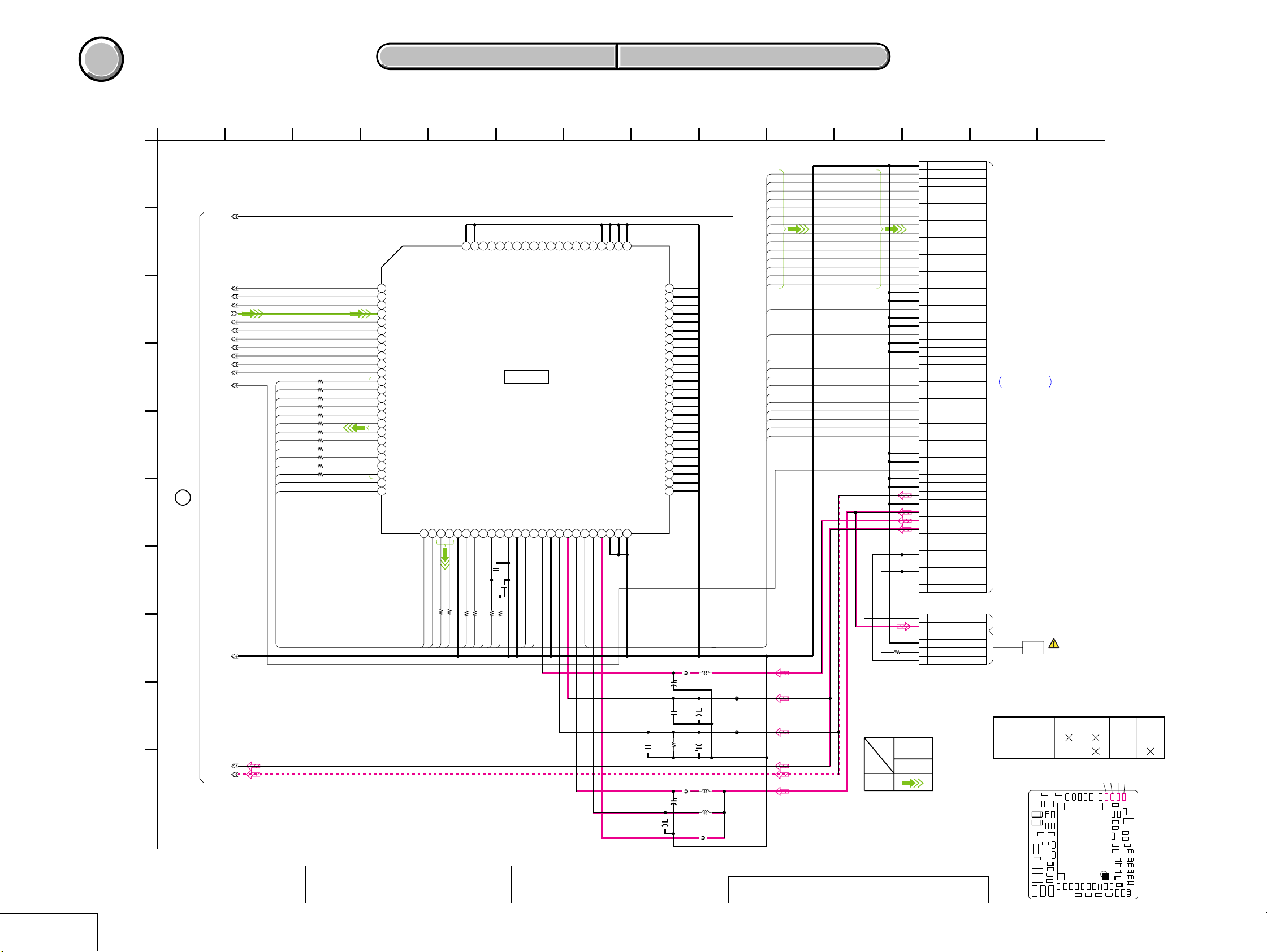
MVC-CD250/CD400
COVER
COVER
For Schematic Diagram
• Refer to page 4-53 for printed wiring board.
4-2. SCHEMATIC DIAGRAMS CD-393 PRINTED WIRING BOARD
4-2. SCHEMATIC DIAGRAMS CD-393 PRINTED WIRING BOARD
1
CD-393 BOARD (2/2)
A
CAMERA MODULE(MOJYUURU BLOCK)
XX MARK:NO MOUNT
VSUB_CONT
B
H1
H2
C
D
E
1
(1/2)
F
G
H
I
J
05
CCD_OUT
CCD_TEMP
CAM_15V
CAM_-7.5V
VSHT
RG
V1A
V1B
V2
V3A
V3B
V4
GND
D3
D4
D5
D6
D7
D8
D9
D10
D11
D12
D13
XTG_CS
XGCAM_CS
3
5
7
91411 126842
(MVC-CD400)
7677787980818283848586878889909192939495
12345678910111213141516171819202122232425
R505
150
R506
150
R507
150
R508
150
R509
150
R510
150
R511
150
R512
150
R513
150
R514
150
R515
150
R516
150
26 27 28 29 30 31 32 33 34 35 36 37 38 39 40 41 42 43 44 45 46 47 48 49 50
XCAM_SO
XCAM_SCKD1D0
Note:The voltage and waveform of CSP(chip size package)
cannot be measured,because its lead layout is different
form that of conventional IC.
150
150
XX
R518
R517
R524XXR523
CLPOB
CLPDM
XX
C508
220
R519
XCAM_RESET
CA_HD1
IC501
CAMERA MODULE
IC501
(CH-111 BOARD)
XX
C509
220
R520
CA_FD1D2MCK12
TG_CLK
TG_WEN
51 52 53 54 55 56 57 58 59 60 61 62 63 64 65 66 67 68 69 70 71 72 73 74 75
L503
47uH
FB502
C504
33u
10V
C506
C505
6.8u
0.1u
35V
C507
R502
C501
100k
0.1u
C503
6.3V
22u
16V
FB501
C502
47u
6.3V
47u
FB503
FB504
FB505
L501
47uH
L502
47uH
D0
D1
D2
D3
D4
D5
D6
D7
D8
D9
D10
D11
D12
D13
TG_CLK
MCK12
XGCAM_CS
XCAM_SO
XCAM_SCK
XTG_CS
TG_WEN
CLPDM
CLPOB
CA_FD1
CA_HD1
XCAM_RESET
10
R530 10
SIGNAL PATH
Y/CHROMA
REC
VIDEO
SIGNAL
CN501
10
11
12
13
14
15
16
17
18
19
20
21
22
23
24
25
26
27
28
29
30
31
32
33
34
35
36
37
38
39
40
41
42
43
44
45
46
47
48
49
50
51
1
2
3
4
5
6
7
8
9
6
5
4
3
2
1
51P
CD_GND
CA_AD0
CA_AD1
CA_AD2
CA_AD3
CA_AD4
CA_AD5
CA_AD6
CA_AD7
CA_AD8
CA_AD9
CA_AD10
CA_AD11
CA_AD12
CA_AD13
CD_GND
CD_GND
TG_CLK
CD_GND
CD_GND
MCK12
CD_GND
CD_GND
XGCAM_CS
CAM_SO
XCAM_SCK
XTG_CS
TG_WEN
CLPDM
CLPOB
CA_FD
CA_HD
XCAM_RESET
VSUB_CONT
CD_GND
CD_GND
CCD_TEMP
CD_GND
CD_GND
CAM_-7.5V
REG_GND
CAM_3.1V
CAM_5V
CAM_15V
XLENSCAP_ON
PD_OUT
PD_OUT
LD_OUT
LD_OUT
N.C.
N.C.
6PCN502
XLENSCAP_ON
CAM_3.1V
N,C
REG_GND
LD_OUT
PD_OUT
13
SY-76 (1/13)
CN724
THROUGH THE
FP-484 FLEXIBLE
(PAGE 4-15)
:CD400
LS-61
CN801
(THROUGH THE FP-490 FLEXIBLE)
(PAGE 4-49)
FP-490
FLEXIBLE
LASER
UNIT D9001
(Note 1)
Note: Each model has its own camera module.
Discrimination method is the following.
ABCD
MVC-CD250 aa
MVC-CD400 aa
IC501
(CH-111 BOARD)
ABCD
CD-393 (2/2)
The components identified by mark 0 or dotted
line with mark 0 are critical for safety.
Replace only with part number specified.
4-9
Les composants identifiés par une marque 0 sont
critiques pour la sécurité. Ne les remplacer que
par une piéce portant le numéro spécifié.
(Note 1) Be sure to read “SERVICE NOTE” on page 1-2 when
replacing the laser unit (D9001).
4-10
 Loading...