

Sony BRAVIA KDL-40V2500, BRAVIA KDL-46V2500, BRAVIA KDL-46V25L1 Service Manual

HISTORY INFORMATION FOR THE FOLLOWING MANUAL:
SERVICE MANUAL
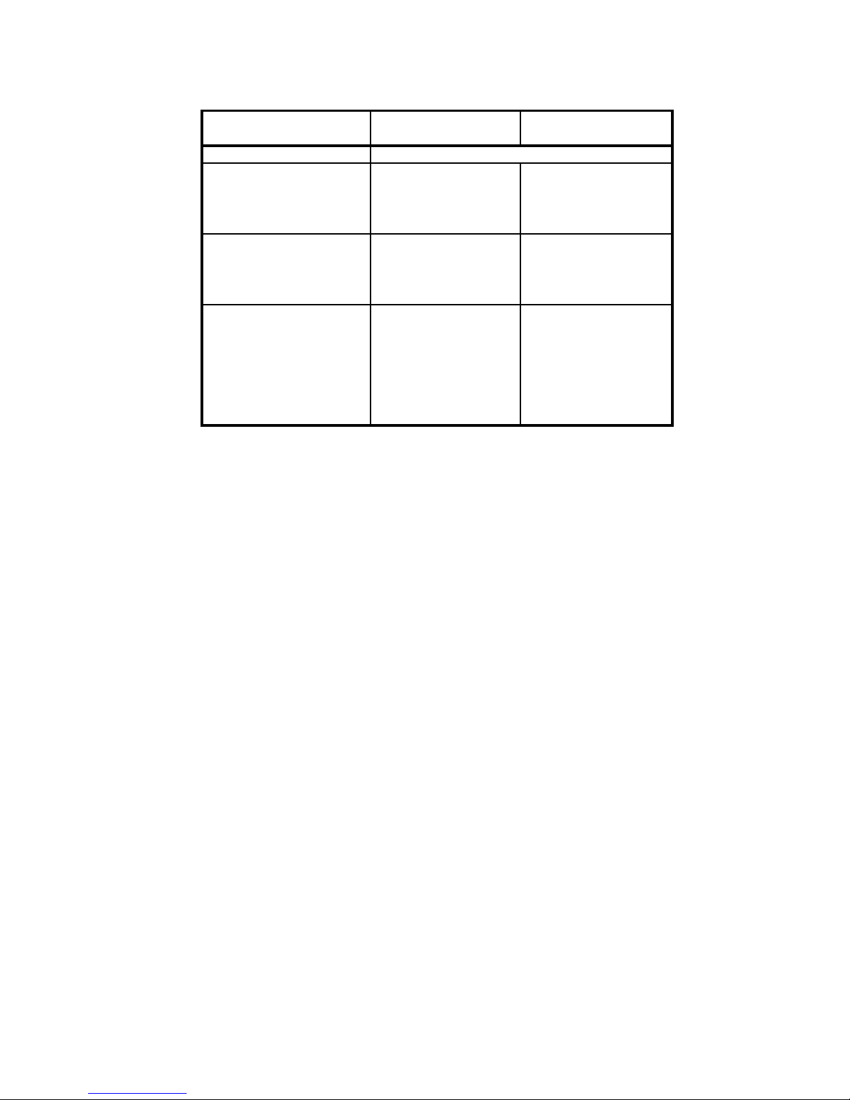
MODEL NAME REMOTE COMMANDER DESTINATION
KDL-40V2500
KDL-40V2500
KDL-46V2500
KDL-46V2500
KDL-46V25L1
RM-YD012 CANADA
RM-YD012 US
RM-YD012 CANADA
RM-YD012 US
RM-YD012 US
WAX2F
CHASSIS
ORIGINAL MANUAL ISSUE DATE: 9/2006
REVISION DATE SUBJECT
9/2006 No revisions or updates are applicable at this time.
9/2006 Added APPENDIX A: ENCRYPTION KEY COMPONENTS to service manual. Added Page A-1
Updated Table of Contents. Replaced page 3
Updated Encryption Key notes. Replaced pages 23, 54-58, and 64
1/2007 Updated Block Diagram to show correct Boards. Replaced page 25.
:UPDATED ITEM
☛
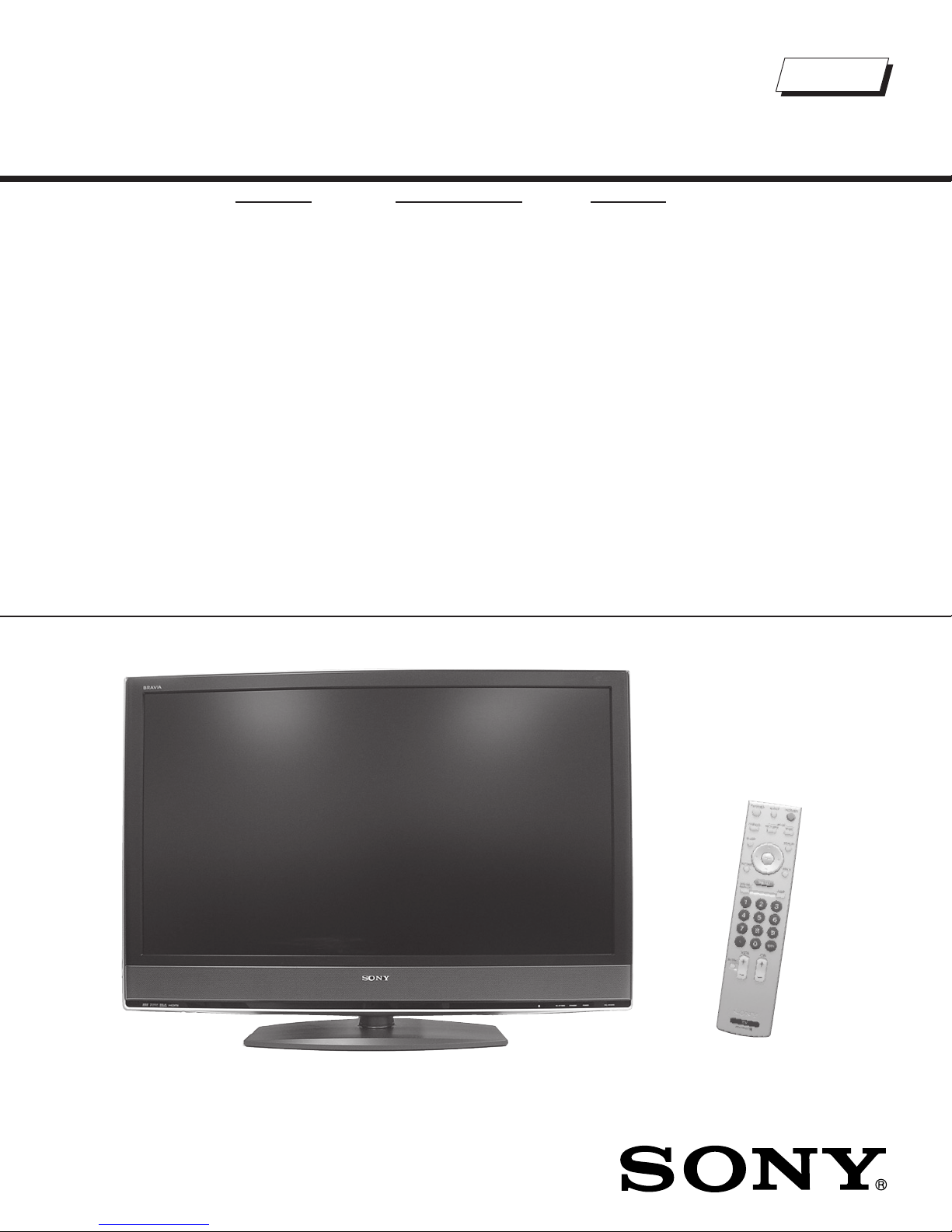
LCD DIGITAL COLOR TELEVISION
9-883-722-03
Self Diagnosis
Supported model
SERVICE MANUAL
MODEL NAME REMOTE COMMANDER DESTINATION
KDL-40V2500
KDL-40V2500
KDL-46V2500
KDL-46V2500
KDL-46V25L1
RM-YD012 CANADA
RM-YD012 US
RM-YD012 CANADA
RM-YD012 US
RM-YD012 US
WAX2F
CHASSIS
9-883-722-03
KDL-40V2500 RM-YD012
LCD DIGITAL COLOR TELEVISION

KDL-40V2500/46V2500/46V25L1
TABLE OF CONTENTS
SECTION TITLE PAGE SECTION TITLE PAGE
Specifi cations ................................................................................. 4
Warnings and Cautions .................................................................. 6
Safety-Related Component Warning .............................................. 7
Safety Check-Out ........................................................................... 9
Self-Diagnostic Function ............................................................... 10
SECTION 1: DISASSEMBLY ............................................................... 12
1-1. Rear Cover Removal ............................................... 12
1-2. Vesa Bracket Assembly and Stand Removal ........... 13
1-3. H1U Board Removal ................................................ 14
1-4. G2A Board Removal ................................................ 14
1-5. H2U Board Removal ................................................ 15
1-6. AU Board Removal .................................................. 15
1-7. QT Board Removal .................................................. 16
1-8. H3U Board and Speaker Removal .......................... 16
1-9. QSF board and BU Board Removal ........................ 17
1-10. LCD Panel Removal ................................................ 18
SECTION 2: SERVICE ADJUSTMENTS ............................................. 19
2-1. Remote Adjustment Buttons and Indicators ......................... 19
2-2. Accessing Service Adjustments ........................................... 19
2-2-1. Accessing the Digital Service Adjustment Menus .... 19
2-2-2. Viewing the Digital Module Box (Q-Box)
Service Items ........................................................... 20
2-2-3. Accessing the Analog Service Adjustment Menus ... 20
2-3. Resetting the User Menu - Factory Reset ............................ 21
2-4. Aging Mode .......................................................................... 21
2-5. White Balance Adjustment. .................................................. 22
SECTION 3: DIAGRAMS ..................................................................... 23
3-1. Circuit Boards Location ........................................................ 23
3-2. Printed Wiring Boards and
Schematic Diagrams Information ......................................... 23
3-3. Block Diagram ...................................................................... 25
3-4. Schematics and Supporting Information .............................. 26
AU Board Schematic Diagram (1 of 2) ................................. 26
AU Board Schematic Diagram (2 of 2) ................................. 27
BU Board Schematic Diagram (1 of 9) ................................. 29
BU Board Schematic Diagram (2 of 9) ................................. 30
BU Board Schematic Diagram (3 of 9) ................................. 31
BU Board Schematic Diagram (4 of 9) ................................. 32
BU Board Schematic Diagram (5 of 9) ................................. 33
BU Board Schematic Diagram (6 of 9) ................................. 34
BU Board Schematic Diagram (7 of 9) ................................. 35
BU Board Schematic Diagram (8 of 9) ................................. 36
BU Board Schematic Diagram (9 of 9) ................................. 37
G2A Board Schematic Diagram ........................................... 39
H1U Board Schematic Diagram ........................................... 41
H2U Board Schematic Diagram ........................................... 42
H3U Board Schematic Diagram ........................................... 44
QSF Board Schematic Diagram (1 of 5) .............................. 45
QSF Board Schematic Diagram (2 of 5) .............................. 46
QSF Board Schematic Diagram (3 of 5) .............................. 47
QSF Board Schematic Diagram (4 of 5) .............................. 48
QSF Board Schematic Diagram (5 of 5) .............................. 49
QT Board Schematic Diagram ............................................. 51
3-5. Semiconductors ................................................................... 53
SECTION 4: EXPLODED VIEWS ........................................................ 54
4-1. Rear Cabinet and Stand Assembly ..................................... 54
4-2. Chassis ............................................................................... 55
4-3. Speakers .............................................................................. 56
4-4. LCD Panel ............................................................................ 57
SECTION 5: ELECTRICAL PARTS LIST ............................................ 58
APPENDIX A: ENCRYPTION KEY COMPONENTS ..........................A-1
KDL-40V2500/46V2500/46V25L1
3

SPECIFICATIONS
y
KDL-40V2500/46V2500/46V25L1
Power Requirements:
Power Consumption (W):
In Use (Max):
In Standby :
120V-240V AC, 50/60Hz
200W (KDL-40V2500 Only)
240W (KDL-46V2500/46V25L1 Only)
Less than 0.1W
Video (IN) 1/2/3:
S Video (4-Pin Mini DIN (VIDEO 1/2 Only):
Y: 1.0 Vp-p, 75 ohms unbalanced, sync negative
C: 0.286 Vp-p (Burst signal), 75 ohms
Video:
1.0 Vp-p, 75ohms unbalanced, sync negative
Audio:
500 mVrms (100% modulation)
Impedance:47 kilohms
HD/DVD IN 4/5:
YP
(Component Video):
BPR
Y:1.0 Vp-p, 75 ohms unbalanced, sync negative
PB:0.7 Vp-p, 75 ohms
PR:0.7 Vp-p, 75 ohms
Signal format: 480i, 480p, 720p, 1080i
AUDIO:
500 mVrms (100% modulation)
Impedance: 47 kilohms
HDMI IN 6/7:
HDMI: Video:480i, 480p, 720p, 1080i, 1080p
Audio: Two channel linear PCM 32, 44.1 and
48 kHz, 16, 20 and 24 bits
AUDIO (HDMI IN 6 Only):
500 mVrms (100% modulation)
Impedance: 47 kilohms
AUDIO OUT:
500 mVrms (100% modulation)
More than 1 Vrms at the maximum volume setting (Variable)
More than 500 mVrms (Fixed)
PC IN 8:
D-sub 15-pin, analog RGB, 0.7 Vp-p, 75 ohms, positive
PC AUDIO INPUT:
Stereo mini jack, 0.5 Vrms, 1 kilohm
Headphones:
Stereo mini jack
Impedance: 16 ohms
Speaker:
Full range: 5.5 × 15 cmm (2
Full range: 7 × 13 cm (2
1/4
× 6 inches) (2) (KDL-40V2500)
3/4
7/16
× 5
inches) (2)
(KDL-46V2500/46V25L1)
Trademark Information
TruSurround XT, SRS and ( ) symbol are trademarks of SRS Labs, Inc.
TruSurround XT technology is incorporated under license from SRS Labs ,
Inc.
Manufactured under license from BBE Sound, Inc.
Licensed by BBE Sound, Inc. under one or more of the following US
patents: 5510752, 5736897. BBE and BBE symbol are registered
trademarks of BBE Sound, Inc.
Macintosh is a trademark licensed to Apple Computer, Inc., registered in
the U.S.A and other countries.
“BRAVIA” and are trademarks of Sony Corporation.
®
As an ENERGY STAR
determined that this product meets the E NERGY STAR
guidelines for energy efficiency.
ENERGY STAR
This TV incorporates High-Definition
HDMI, the HDMI logo and High-Definition Multimedia Interface are
trademarks or registered trademarks of HDMI Licensing, LLC.
Multimedia Interface (HDMI™) technology.
Manufactured under license from Dolby
Laboratories. “Dolby” and the double-D symbol are
trademarks of Dolb
Partner, Sony Corporation has
®
is a U.S. registered mark.
Laboratories.
KDL-40V2500/46V2500/46V25L1
®
Design and specifi cations are subject to change without notice.
4
KDL-40V2500/46V2500/46V25L1
Television system
American TV Standard
ATSC compliant 8VSB
ANSI/SCTE 07 2000
(Does not include CableCARD functionality)
Channel coverage
Analog Digital
Terrestrial 2-69 2-69
Cable 1-125 1-135
Antenna
75-ohm external terminal for VHF/UHF
Panel System
LCD (Liquid Crystal Display) Panel
Display Resolution (horizontal x vertical):
1,920 dots x 1,080 lines
Screen Size (measured diagonally)
Supplied Accessories
Optional Accessories
40 inches (KDL-40V2500 Only)
46 inches (KDL-46V2500/46V25L1 Only)
Remote Commander RM-YD012
Two Size AA (R6) Batteries
75-ohm coaxial cable
AC Power Cord
HD15-HD15 Cable
Suport Belt, Securing Screw, and Wood Screw
Cable Holder
Operating Instructions
Quick Setup Guide
Warranty Card
Headphones Plug Adaptor
Connecting Cables
Wall-Mount Bracket
SU-WL51
KDL-40V2500/46V2500/46V25L1
5
KDL-40V2500/46V2500/46V25L1
WARNINGS AND CAUTIONS
CAUTION
These servicing instructions are for use by qualifi ed service personnel only. To reduce the risk of electric shock, do not perform any
servicing other than that contained in the operating instructions unless you are qualifi ed to do so.
WARNING!!
An isolation transformer should be used during any service to avoid possible shock hazard, because of live chassis. The chassis of
this receiver is directly connected to the ac power line.
!
SAFETY-RELATED COMPONENT WARNING!!
Components identifi ed by shading and ! mark on the schematic diagrams, exploded views, and in the parts list are critical for
safe operation. Replace these components with Sony parts whose part numbers appear as shown in this manual or in supplements
published by Sony. Circuit adjustments that are critical for safe operation are identifi ed in this manual. Follow these procedures
whenever critical components are replaced or improper operation is suspected.
ATTENTION!!
Ces instructions de service sont à l’usage du personnel de service qualifi é seulement. Pour prévenir le risque de choc électrique, ne
pas faire l’entretien autre que celui contenu dans le Mode d’emploi à moins que vous soyez qualifi é faire ainsi.
Afi n d’eviter tout risque d’electrocution provenant d’un chássis sous tension, un transformateur d’isolement doit etre utilisé lors de tout
dépannage. Le chássis de ce récepteur est directement raccordé à l’alimentation du secteur.
!
ATTENTION AUX COMPOSANTS RELATIFS A LA SECURITE!!
Les composants identifi es par une trame et par une marque ! sur les schemas de principe, les vues explosees et les listes de
pieces sont d’une importance critique pour la securite du fonctionnement. Ne les remplacer que par des composants Sony dont
le numero de piece est indique dans le present manuel ou dans des supplements publies par Sony. Les reglages de circuit dont
l’importance est critique pour la securite du fonctionnement sont identifi es dans le present manuel. Suivre ces procedures lors de
chaque remplacement de composants critiques, ou lorsqu’un mauvais fonctionnement suspecte.
KDL-40V2500/46V2500/46V25L1
6
KDL-40V2500/46V2500/46V25L1
SAFETY-RELATED COMPONENT WARNING
There are critical components used in LCD color TVs that are important for safety. These components are identifi ed with shading and
mark on the schematic diagrams and the electrical parts list. It is essential that these critical parts be replaced only with the part number
specifi ed in the electrical parts list to prevent electric shock, fi re, or other hazard.
NOTE: Do not modify the original design without obtaining written permission from the manufacturer or you will void the original parts and
labor guarantee.
!
USE CAUTION WHEN HANDLING THE LCD PANEL
When repairing the LCD panel, be sure you are grounded by using a wrist band.
When installing the LCD panel on a wall, the LCD panel must be secured using the 4 mounting holes on the rear cover.
To avoid damaging the LCD panel:
do not press on the panel or frame edge to avoid the risk of electric shock.
do not scratch or press on the panel with any sharp objects.
do not leave the module in high temperatures or in areas of high humidity for an extended period of time.
do not expose the LCD panel to direct sunlight.
avoid contact with water. It may cause a short circuit within the module.
disconnect the AC adapter when replacing the backlight (CCFL) or inverter circuit.
(High voltage occurs at the inverter circuit at 650Vrms.)
always clean the LCD panel with a soft cloth material.
use care when handling the wires or connectors of the inverter circuit. Damaging the wires may cause a short.
protect the panel from ESD to avoid damaging the electronic circuit (C-MOS).
LEAKAGE CURRENT HOT CHECK CIRCUIT
KDL-40V2500/46V2500/46V25L1
7
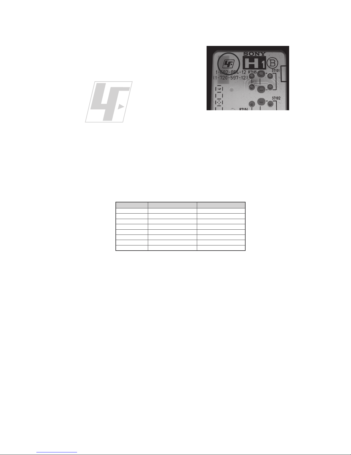
The circuit boards used in these models have been processed using
Lead Free Solder. The boards are identified by the LF logo located
close to the board designation e.g. H1 etc [ see example ]. The
servicing of these boards requires special precautions to be taken as
outlined below.
KDL-40V2500/46V2500/46V25L1
example 1
It is strongly recommended to use Lead Free Solder material in order to guarantee optimal quality of new solder joints.
Lead Free Solder is available under the following part numbers :
rebmuntraP retemaiD skrameR
91-500-046-7mm3.0gK52.0
02-500-046-7mm4.0gK05.0
12-500-046-7mm5.0gK05.0
22-500-046-7mm6.0gK52.0
32-500-046-7mm8.0gK00.1
42-500-046-7mm0.1gK00.1
52-500-046-7mm2.1gK00.1
62-500-046-7mm6.1gK00.1
Due to the higher melting point of Lead Free Solder the soldering iron tip temperature needs to be set to 370 degrees centigrade.
This requires soldering equipment capable of accurate temperature control coupled with a good heat recovery characteristics.
For more information on the use of Lead Free Solder, please refer to
http://www.sony-training.com
KDL-40V2500/46V2500/46V25L1
8
SAFETY CHECK-OUT
KDL-40V2500/46V2500/46V25L1
After correcting the original service problem, perform the following
safety checks before releasing the set to the customer:
1. Check the area of your repair for unsoldered or poorly soldered
connections. Check the entire board surface for solder splashes and
bridges.
2. Check the interboard wiring to ensure that no wires are “pinched” or
touching high-wattage resistors.
3. Check that all control knobs, shields, covers, ground straps, and
mounting hardware have been replaced. Be absolutely certain that
you have replaced all the insulators.
4. Look for unauthorized replacement parts, particularly transistors,
that were installed during a previous repair. Point them out to the
customer and recommend their replacement.
5. Look for parts which, though functioning, show obvious signs of
deterioration. Point them out to the customer and recommend their
replacement.
6. Check the line cords for cracks and abrasion. Recommend the
replacement of any such line cord to the customer.
7. Check the antenna terminals, metal trim, “metallized” knobs, screws,
and all other exposed metal parts for AC leakage. Check leakage as
described below.
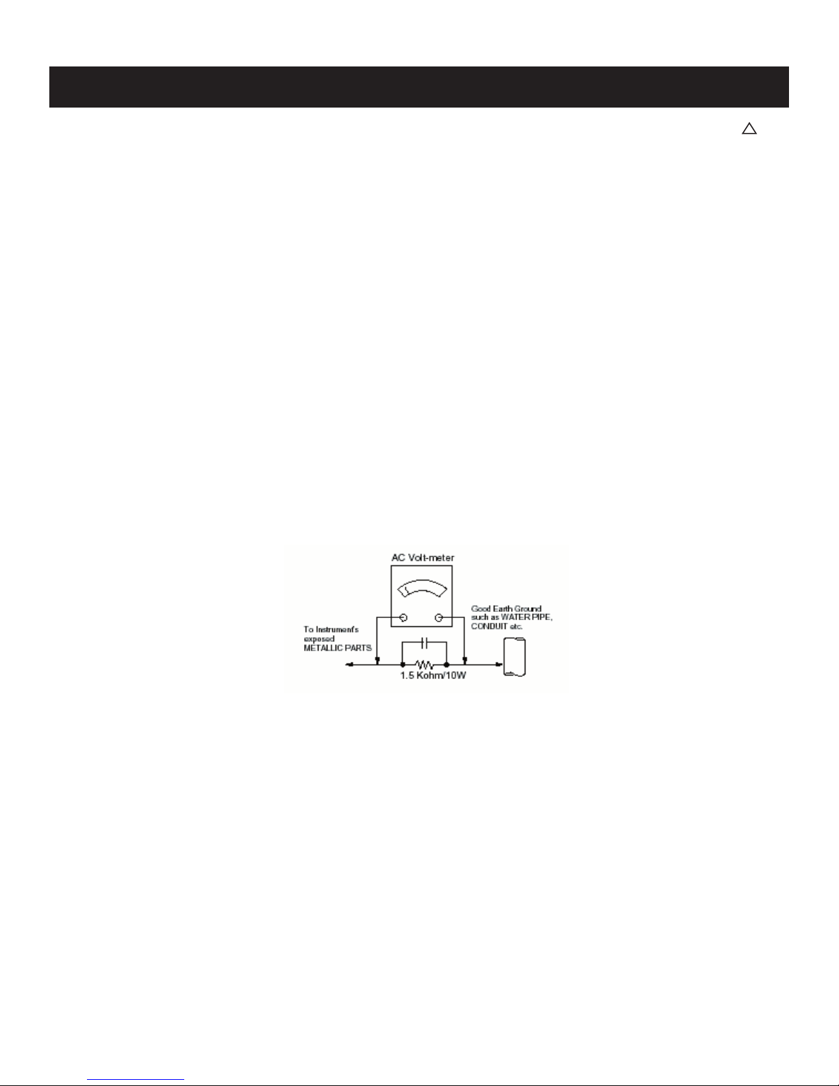
The AC leakage from any exposed metal part to earth ground and
from all exposed metal parts to any exposed metal part having a
return to chassis, must not exceed 0.5 mA (500 microamperes).
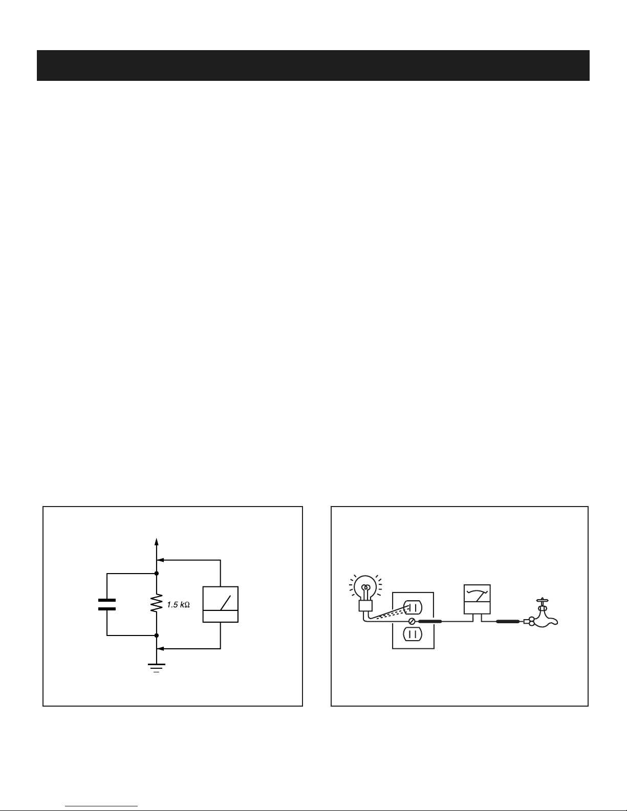
Leakage current can be measured by any one of three methods.
1. A commercial leakage tester, such as the Simpson 229 or RCA
WT-540A. Follow the manufacturers’ instructions to use these
instructions.
2. A battery-operated AC milliampmeter. The Data Precision 245
digital multimeter is suitable for this job.
3. Measuring the voltage drop across a resistor by means of a VOM
or battery-operated AC voltmeter. The “limit” indication is 0.75
V, so analog meters must have an accurate low voltage scale.
The Simpson’s 250 and Sanwa SH-63TRD are examples of
passive VOMs that are suitable. Nearly all battery-operated digital
multimeters that have a 2 VAC range are suitable (see Figure A).
How to Find a Good Earth Ground
A cold-water pipe is a guaranteed earth ground; the cover-plate
retaining screw on most AC outlet boxes is also at earth ground. If the
retaining screw is to be used as your earth ground, verify that it is at
ground by measuring the resistance between it and a cold-water pipe
with an ohmmeter. The reading should be zero ohms.
If a cold-water pipe is not accessible, connect a 60- to 100-watt
trouble- light (not a neon lamp) between the hot side of the receptacle
and the retaining screw. Try both slots, if necessary, to locate the hot
side on the line; the lamp should light at normal brilliance if the screw
is at ground potential (see Figure B).
Leakage Test
0.15 µF
Figure A. Using an AC voltmeter to check AC leakage. Figure B. Checking for earth ground.
To Exposed Metal
Parts on Set
Earth Ground
AC
Voltmeter
(0.75V)
Trouble Light
AC Outlet Box
Ohmmeter
Cold-water Pipe
KDL-40V2500/46V2500/46V25L1
9
KDL-40V2500/46V2500/46V25L1
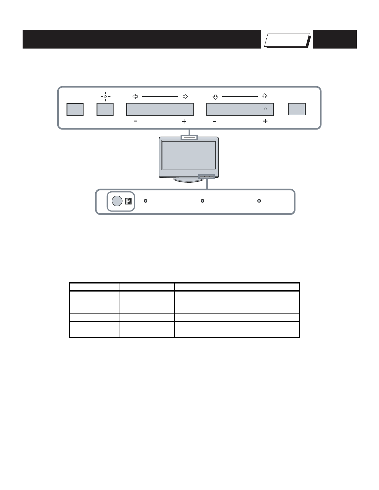
Control Buttons
MENU
TV/VIDEO
SELF-DIAGNOSTIC FUNCTION
VOLUME
PIC OFF/TIMER STANDBY POWER
CHANNEL
Self Diagnosis
Supported model
POWER
Description of LED Indictors
LED LED Type Description
POWER LED Red/Green LED
TIMER LED Red LED Lights when timer is set
PIC OFF LED Green LED
* Light is green when the TV set is on
* Functions as failure indicator
* Blinks green in aging mode
Lights when power saving setting is set to
picture off (See Instruction Manual)
KDL-40V2500/46V2500/46V25L1
10
LED Control
KDL-40V2500/46V2500/46V25L1
The units in this manual contain a self-diagnostic function. If an error occurs, the POWER LED will automatically begin to fl ash. The number of times
the LED fl ashes translates to a probable source of the problem. A defi nition of the POWER LED fl ash indicators is listed in the instruction manual for
the user’s knowledge and reference. If an error symptom is diffi cult to reproduced use the Remote Commander to display the record that is stored at
the internal NVM to specify the cause of the failure.
Diagnostic Test Indicators
When an error occurs, the POWER LED will fl ash a set number of times to indicate the possible cause of the problem. If there is more than one error,
the LED will identify the fi rst of the problem areas. If the errors occur simultaneously, the one that corresponds to the fewest fl ashes is identifi ed fi rst.
Results for all of the following diagnostic items are displayed on screen. No error has occurred if the screen displays a “0”.
KDL-40V2500/46V2500/46V25L1
11
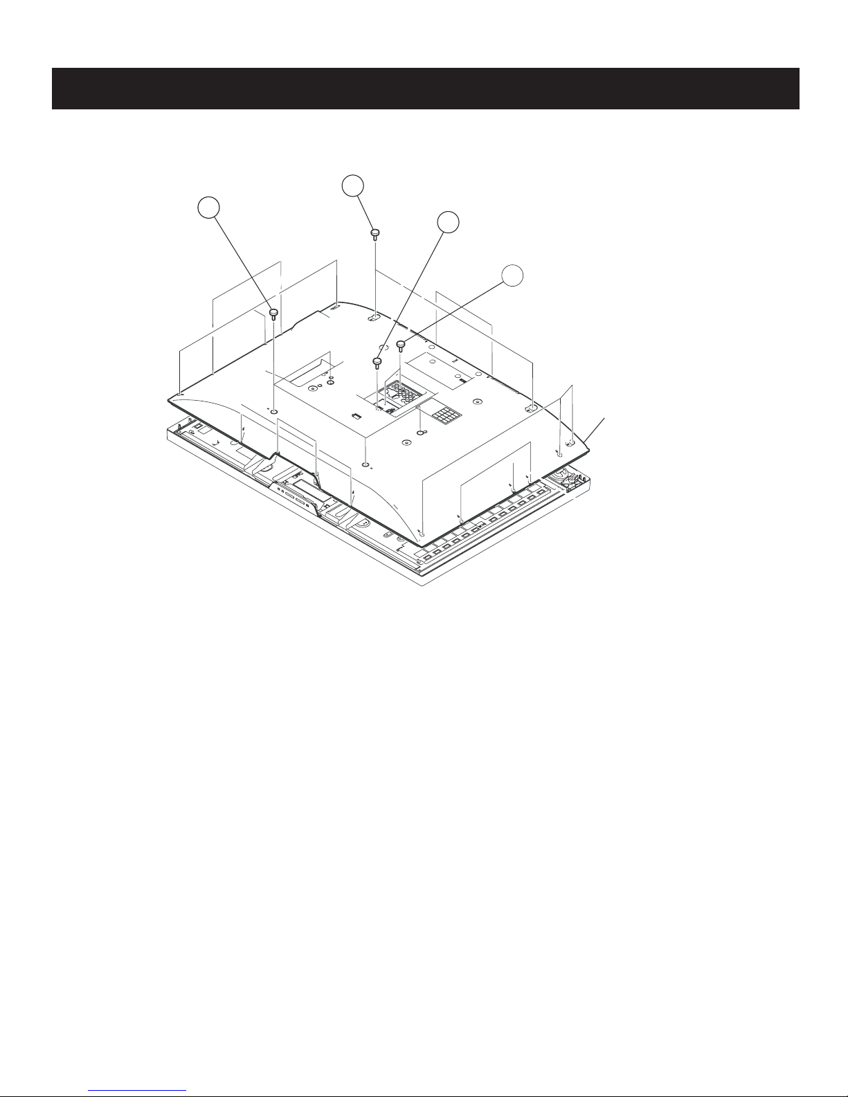
1-1. REAR COVER REMOVAL
4 Screws,
1
+PSW M6X16
SECTION 1: DISASSEMBLY
12 Screws, +BVTP2 4X16 (KDL-40V2500 ONLY)
2
18 Screws, +BVTP2 4X16 (KDL-46V2500/46V25L1)
5 Screws,
3
+PSW M3X5
4
+BVPT 3X12 TYPE2 IT-3
5 Screws,
KDL-40V2500/46V2500/46V25L1
Rear Cover
KDL-40V2500/46V2500/46V25L1
12
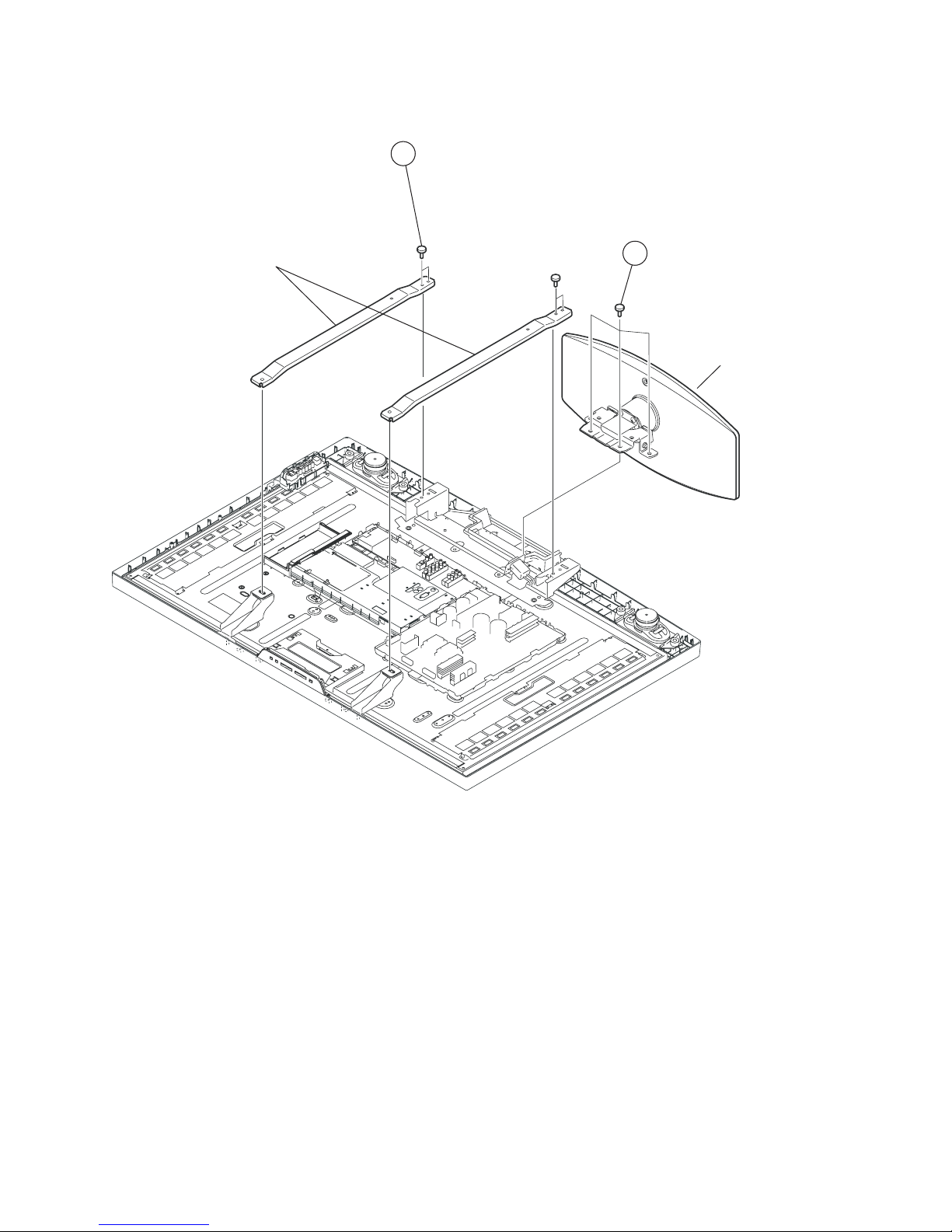
1-2. VESA BRACKET ASSEMBLY AND STAND REMOVAL
4 Screws,
1
+PSW M4X16
VESA Bracket Assembly
4 Screws,
2
+PSW M5X16
KDL-40V2500/46V2500/46V25L1
Stand Assembly
KDL-40V2500/46V2500/46V25L1
13
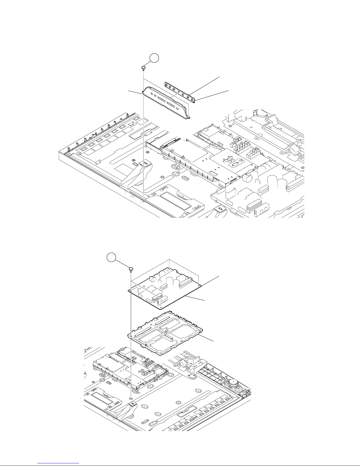
1-3. H1U BOARD REMOVAL
2 Screws,
1
+BVTP2 4X16
KDL-40V2500/46V2500/46V25L1
Disconnect CN1101
Multi Button Assy
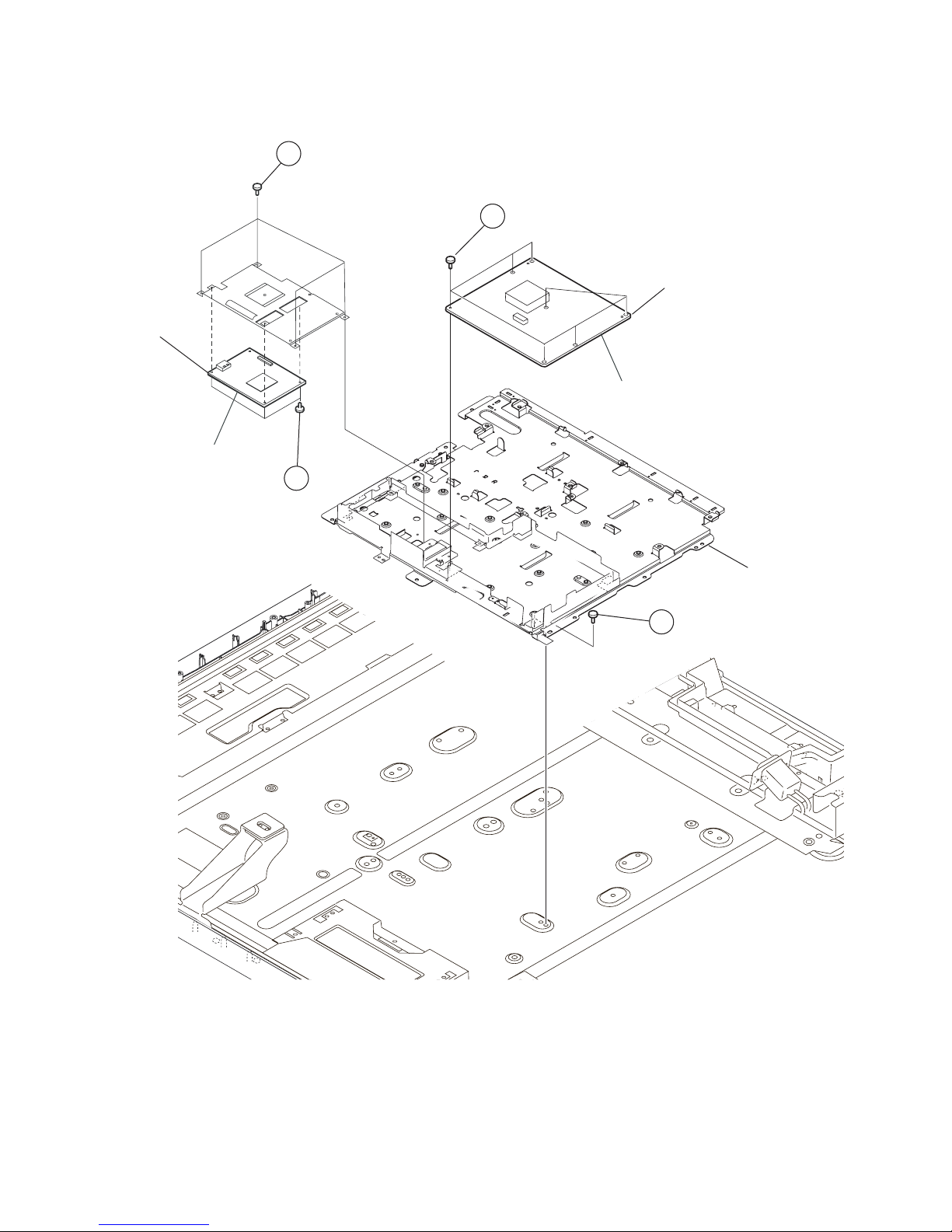
1-4. G2A BOARD REMOVAL
4 Screws,
+PSW 3SG
1
H1U Board
G2A board
4 Connectors
CN6001, CN6200, CN6202
and CN6217
G2 Bracket
KDL-40V2500/46V2500/46V25L1
14
1-5. H2U BOARD REMOVAL
KDL-40V2500/46V2500/46V25L1
Side Terminal Assembly
2 Screws,
+BVTP 3X12 TYPE2 IT-3
H2U Board
Side Jack Holder
1
One Connector CN1201
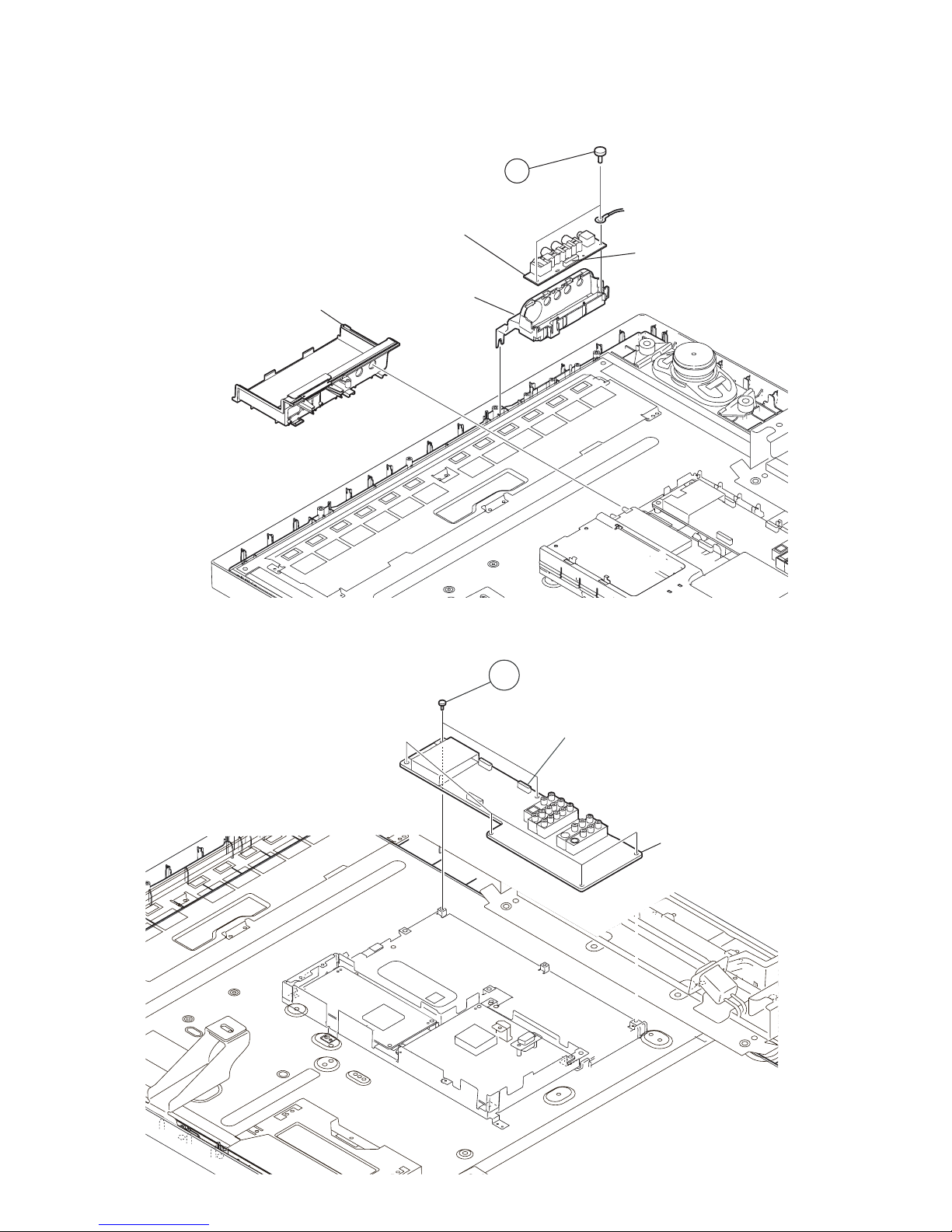
1-6. AU BOARD REMOVAL
6 Screws,
1
+BVST 3x8
Disconnect CN9501, CN9502, CN9001,
CN2500, CN2303, CN2302 and CN2301
AU board
KDL-40V2500/46V2500/46V25L1
15
1-7. QT BOARD REMOVAL
KDL-40V2500/46V2500/46V25L1
One Screw,
+PSW M3x5
1
4 Screws,
2
+BVST 3x8
QT Board
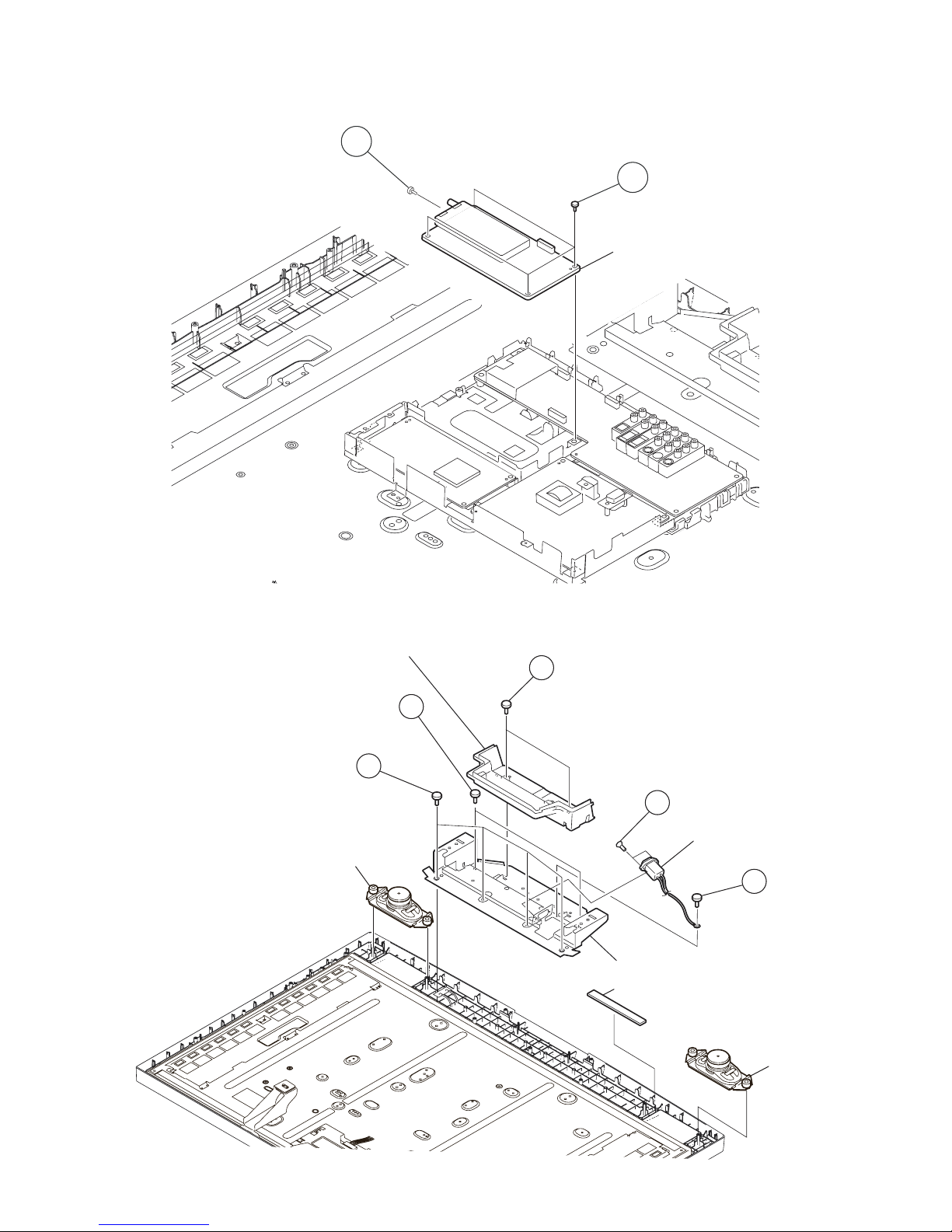
1-8. H3U BOARD AND SPEAKER REMOVAL
Under Cover
2 Screws,
+BVTP2 4X16
4 Screws,
+PSW M5X8
Speaker
2
1
2 Screws,
3
+BVTP2 4X16
2 Screws,
4
+KTT 3X10
AC Inlet
5
Bottom Frame Assembly
H3U Board
One Screw,
+PSW M4X8
Speaker
KDL-40V2500/46V2500/46V25L1
16
1-9. QSF BOARD AND BU BOARD REMOVAL
4 Screws,
1
+BVST 3X8
QSF Board
Disconnect CN7314,
CN7317 and CN7802
3 Screws,
+PSW M3X5
4
7 Screws,
2
+BVST 3X8
KDL-40V2500/46V2500/46V25L1
BU Board
Disconnect CN4001, CN4002, CN4007,
CN4008, CN4701, CN4702, CN4300,
CN5003, CN7003 and CN7008
9 Screws,
3
+PSW M3X5
Chassis Bracket
KDL-40V2500/46V2500/46V25L1
17

1-10. LCD PANEL REMOVAL
Two Screws,
4
+PSW 5X8
Two Screws,
+BVTP2 4X12
Top Frame
5
Two Screws,
1
+BVTP2 4X16
Panel Corner Bracket
Harness with Connector (LVDS)
LCD Panel
KDL-40V2500/46V2500/46V25L1
Two Screws,
2
+BVTP2 4X16
Bezel Assembly
Bezel Support (S)
(46” Panel only)
Bezel Support (L)
(46” Panel only)
Two Screws,
3
+BVTP 3X12
KDL-40V2500/46V2500/46V25L1
18
SECTION 2: SERVICE ADJUSTMENTS
KDL-40V2500/46V2500/46V25L1
2-1. REMOTE ADJUSTMENT BUTTONS AND
INDICATORS
POWER
DISPLAY
Onscreen cursor
and select button
DIGITAL/
ANALOG
5
VOLUME+
2-2. ACCESSING SERVICE ADJUSTMENTS
To adjust various set features, use the Remote Commander to put the set
into service mode to display the service menus. The Remote Commander
displays the service menu associated with the Digital or Analog format
depending on which format is on the TV when you enter service mode.
2-2-1. ACCESSING THE DIGITAL SERVICE
ADJUSTMENT MENUS
1. Turn the TV on and view a Digital channel.
2. Put the TV in standby mode. (Power off).
3. Press the following buttons on the Remote Commander within a
second:
DISPLAY
Channel
The Digital service menu displays.
5
Volume +
MAIN VER. 1009
H PACK VER. 1008
S PACK VER. 1008
CHECK SUM E20E
NVM VER. 1006
ATI VER. 01.06
ATI UD NVM VER. 02
ATI SD NVM VER. 02
ETI 46h 39m
Video 1
POWER
On.
4. Use the button to view the next category listing the white balance
adjustment items.
Video 1
R_DRIVE 256
B_DRIVE 256
R_BKG 512
G_BKG 512
RM-YD012
B_BKG 512
COLOR SAVE
5. Use the or button to select the item you want to adjust.
a. To increase the data value of the category, press the
b. To decrease the data value of the category, press the
6. To save the data value changes, press the
Save and then press the
button.
button to select Color
button.
button.
a. To save the data value changes, select Save by pressing the
button and then press the
button.
b. To cancel the data value changes, select Cancel by pressing
the
button and then pressing the button.
KDL-40V2500/46V2500/46V25L1
19
KDL-40V2500/46V2500/46V25L1
2-2-2. VIEWING THE DIGITAL MODULE BOX
2-2-3. ACCESSING THE ANALOG SERVICE
(Q-BOX) SERVICE ITEMS
Use the following instructions to display the Digital menu items you want
to adjust.
1. Turn the TV on and view a Digital channel.
2. Put the TV in standby mode. (Power off).
3. Press the following buttons on the Remote Commander within a
second:
DISPLAY
Channel
5
Volume +
POWER
On.
The Digital service menu displays.
Video 1
MAIN VER. 1009
H PACK VER. 1008
S PACK VER. 1008
CHECK SUM E20E
NVM VER. 1006
ATI VER. 01.06
ATI UD NVM VER. 02
ATI SD NVM VER. 02
ETI 46h 39m
4. To display the Digital Module (Q Box) service adjustment menus,
JUMP
press
.
The QM category displays.
Category
Data Value
Item #
1. Turn the TV on and view an Analog channel.
2. Put the TV in standby mode. (Power off).
3. Press the following buttons on the Remote Commander within a
The Analog service menu displays.
4. Use the button to view the next category listing the white balance
ADJUSTMENT MENUS
second:
DISPLAY
Channel
adjustment items.
5
MAIN VER. 1008
H PACK VER. 1005
S PACK VER. 1008
CHECK SUM F99F
NVM VER. 1006
ATI VER.
ATI UD NVM VER.
ATI SD NVM VER. 02
ETI 2h 16m
R_DRIVE 256
B_DRIVE 256
R_BKG 512
G_BKG 512
B_BKG 512
COLOR SAVE
Volume +
Video 1
Video 1
POWER
On.
QM
0
0
SERVICE
DTVINFO
Item
Sample DMB (Q Box) Service Menu
5. To change the category, press 2 or 5 on the Remote Commander.
Note: Pressing 2 or 5 only changes the categories within the service
menu displayed. To return to the Digital Service Menu, press the
JUMP
button.
6. To change the adjustment item, press 1 or 4 on the Remote
Commander.
7. To change the data value, press 3 or 6 on the Remote Commander.
Note: To go back to the last saved data value, press 0 then
ENTER
on the Remote Commander to read the memory.
8. To write into memory, press
MUTING
then
ENT
on the Remote
Commander.
9. To exit service mode, turn the power off.
5. Use the or button to select the item you want to adjust.
a. To increase the data value of the category, press the
b. To decrease the data value of the category, press the
button.
button.
6. To save the data value changes, press the
Save and then press the
button.
button to select Color
a. To save the data value changes, select Save by pressing the
button and then press the button.
b. To cancel the data value changes, select Cancel by pressing
the
button and then pressing the button.
KDL-40V2500/46V2500/46V25L1
20
KDL-40V2500/46V2500/46V25L1
2-3. RESETTING THE USER MENU - FACTORY
RESET
The TEST RESET option resets all the customer adjustable data back to the
factory defaults.
1. Put the TV in standby mode. (Power off).
2. Press the following buttons on the Remote Commander within a second:
DISPLAY
Channel
The service menu displays.
5
Volume +
MAIN VER. 1009
H PACK VER. 1008
S PACK VER. 1008
CHECK SUM E20E
NVM VER. 1006
ATI VER. 01.06
ATI UD NVM VER. 02
ATI SD NVM VER. 02
ETI 46h 39m
Video 1
POWER
On.
2-4. AGING MODE
Aging mode is designed to remove image retention from the screen.
NOTE: Once you enter into Aging Mode the Remote Commander no
longer functions with the set. To turn off the set, push the Power Button
on the set.
1. Put the TV in standby mode. (Power off).
2. Press the following buttons on the Remote Commander within a
second:
The service menu displays.
3. Use the button to view the next category listing the white balance
adjustment items.
R_DRIVE 256
B_DRIVE 256
R_BKG 512
G_BKG 512
B_BKG 512
COLOR SAVE
Video 1
3. Use the button to view the next category listing the white balance
adjustment items.
DISPLAY
Channel
5
Volume +
MAIN VER. 1009
H PACK VER. 1008
S PACK VER. 1008
CHECK SUM E20E
NVM VER. 1006
ATI VER. 01.06
ATI UD NVM VER. 02
ATI SD NVM VER. 02
ETI 46h 39m
R_DRIVE 256
B_DRIVE 256
R_BKG 512
G_BKG 512
B_BKG 512
COLOR SAVE
Video 1
Video 1
POWER
On.
4. Continue pressing the button until the next category list displays.
Video 1
TEST RESET
AGING MODE Off
AUTO SHUT-OFF On
ETI CLEAR
INFORMATION RESET
SOUND MUTE On
5. Press the button to select TEST RESET options.
6. Press the
7. Press the
button to select OK.
button to reset the TV.
4. Continue pressing the button until the next category list displays.
Video 1
TEST RESET
AGING MODE Off
AUTO SHUT-OFF On
ETI CLEAR
INFORMATION RESET
SOUND MUTE On
5. Press the button to select AGING MODE.
6. Press the
7. Press the
8. Press the
button to display the Aging Mode options.
button to select ON.
button to start the aging process.
KDL-40V2500/46V2500/46V25L1
21
KDL-40V2500/46V2500/46V25L1
2-5. WHITE BALANCE ADJUSTMENT
.
The White Balance only needs to be adjusted when you replace the BU
Board.
1. Through the Video 1 input, step Gray Scale with Setup.
2. Press MENU on the Remote Commander.
The User Menu displays.
MENU
External Inputs
Analog Favorites
Digital Favorites
Analog
Digital
Settings
Select from connected equipment
Select:
MENU
Exit:Set:
3. Press the button until Settings is selected, then press the button.
4. From the Picture menu, press the
button to display the picture mode
options.
a. Press the
5. From the Picture menu, press the
button to select Custom, then press the button.
button to select Color
Temperature.
a. Press the
b. Press the
6. From the Picture menu, press the
Settings.
button to display the Color Temperature options.
button to select Cool, then press the button.
button to select Advanced
Picture Video 1
Target Inputs All Inputs
Picture Mode Custom
Reset
Backlight Max
Picture Max
Brightness 50
Color 50
Hue 0
Color Temperature Cool
Sharpness 15
Noise Reduction Low
Advanced Settings
A
A
D
D
MENU
Select:
RETURN
Back: Exit:Set:
7. Using the arrow keys set all the registers in the Advanced Setting
menu to Off.
9. Access the Service Menu by pressing the following buttons on the
Remote Commander within a second:
DISPLAY
Channel
5
Volume +
POWER
On.
The Digital service menu displays.
Video 1
MAIN VER. 1009
H PACK VER. 1008
S PACK VER. 1008
CHECK SUM E20E
NVM VER. 1006
ATI VER. 01.06
ATI UD NVM VER. 02
ATI SD NVM VER. 02
ETI 46h 39m
10. Press the button to display the white balance adjustment menu
items.
R_DRIVE 256
B_DRIVE 256
R_BKG 512
G_BKG 512
B_BKG 512
COLOR SAVE
Video 1
11. Using 10 step NTSC Gray Scale with Setup adjust the White Balance
of the 60% shade with R_Drive and B_Drive.
12. Using the same pattern, adjust the white balance 20% with R_BKG
and B_BKG.
13. 20IRE and 60IRE shades should have the same color.
Picture Video 1
Advanced Settings
Reset
Black Corrector Off
Contrast Enhancer Off
Gamma Off
Clear White Off
Live Color Off
MPEG Noise Reduction Off
A
A
D
D
Select:
RETURN
Back: Exit:Set:
8. Put the TV in standby mode. (Power off).
KDL-40V2500/46V2500/46V25L1
MENU
SET-UP
56mv
20%
188mv
20 IRE Level
60%
451mv
60 IRE Level
10 STEP
GRAY SCALE
22
3-1. CIRCUIT BOARDS LOCATION
KDL-40V2500/46V2500/46V25L1
SECTION 3: DIAGRAMS
H1U Board
QSF Board
H2U Board
QT Board
AU Board
3-2. PRINTED WIRING BOARDS AND
SCHEMATIC DIAGRAMS INFORMATION
All capacitors are in µF unless otherwise noted. pF : µµF 50WV or
less are not indicated except for electrolytics and tantalums.
All electrolytics are in 50V unless otherwise specifi ed.
All resistors are in ohms. kΩ=1000Ω, MΩ=1000kΩ
Indication of resistance, which does not have one for rating
electrical power, is as follows: Pitch : 5mm
Rating electrical power :
1
/
W in resistance, 1/
4
W and 1/
10
W in chip resistance.
16
: nonfl ammable resistor
: fusible resistor
: internal component
: panel designation and adjustment for repair
: earth ground
: earth-chassis
All variable and adjustable resistors have characteristic curve B,
unless otherwise noted.
Readings are taken with a color-bar signal input.
Readings are taken with a 10MΩ digital multimeter.
Voltages are DC with respect to ground unless otherwise noted.
Voltage variations may be noted due to normal production
tolerances.
1
/
W
4
BU Board
G2A Board
H3U Board
All voltages are in V.
S : Measurement impossibility.
: B+line.
: B-line. (Actual measured value may be different).
: signal path. (RF)
Circled numbers are waveform references.
!
The components identifi ed by shading and
only with part number specifi ed.
The symbol indicates a fast operating fuse and is displayed on the component
side of the board. Replace only with fuse of the same rating as marked.
Les composants identifi es per un trame et une marque
securite. Ne les remplacer que par une piece portant le numero specifi e.
Le symbole indique une fusible a action rapide. Doit etre remplace par une
fusible de meme yaleur, comme maque.
NOTE: The components identifi ed by a red outline and a mark contain confi dential
information. Specifi c instructions must be adhered to whenever these components
are repaired and/or replaced.
See Appendix A: Encryption Key Components in the back of this manual.
symbol are critical for safety. Replace
!
sont critiques pour la
KDL-40V2500/46V2500/46V25L1
23
KDL-40V2500/46V2500/46V25L1
REFERENCE INFORMATION
RESISTOR
: RN METAL FILM
: RC SOLID
: FPRD NONFLAMMABLE CARBON
: FUSE NONFLAMMABLE FUSIBLE
: RW NONFLAMMABLE WIREWOUND
: RS NONFLAMMABLE METAL OXIDE
: RB NONFLAMMABLE CEMENT
: ADJUSTMENT RESISTOR
COIL
: LF-8L MICRO INDUCTOR
CAPACITOR
: TA TANTALUM
: PS STYROL
: PP POLYPROPYLENE
: PT MYLAR
: MPS METALIZED POLYESTER
: MPP METALIZED POLYPROPYLENE
: ALB BIPOLAR
: ALT HIGH TEMPERATURE
: ALR HIGH RIPPLE
Terminal name of semiconductors in silk screen
printed circuit ( )
Device Printed symbol Terminal name
Transistor
1
Transistor
2
3
Diode
4
Diode
Diode
5
Diode
6
Diode
7
8
Diode
Diode
9
Diode
0
!¡
Diode
Diode
!™
Transistor
!£
(FET)
Transistor
!¢
(FET)
Transistor
!?
(FET)
Transistor
!§
Transistor
!¶
Transistor
!•
Transistor
!ª
Transistor
@º
Transistor
@¡
Transistor
@™
Transistor
@£
Discrete semiconductot
–
(Chip semiconductors that are not actually used are included.)
*
Collector
Base
Collector
Base
Cathode
Cathode
Anode
Cathode
Anode
Common
Anode
Common
Anode Cathode
Common
Anode
Common
Anode Anode
Common
Cathode
Common
Cathode
Anode
Anode
Cathode
Drain
Drain
B1 E1
C2
B2 C1
E2
B2 E2
C1
B1 C2
E1
B2 E2
C1
B1 C2
E1
B2 E2
C1
B1 C2
E1
E2
B1 E1
C2
(B2)
E1
B1
C1
(B2)
E1
E2
C2
Emitter
Emitter
Anode
(NC)
(NC)
Cathode
Anode
Cathode
Cathode
Cathode
Anode
Anode
Source
Gate
Source
Gate
Source
Drain
Gate
Emitter
Collector
Base
C1(B2)
E2
C2
B1
C1
Circuit
D
G
D
S
B1
B1
B1
B1
B1
B1
D
G
S
S
D
G
C1
E1
C1
E1
E1
C1
E2
C1
C1
G
S
C2
B2
E2
C2
B2
E2
E2
B2
C2
C2C1(B2)
E2
E2E1(B2)
C2
C2E1(B2)
C2
Ver.1.6
KDL-40V2500/46V2500/46V25L1
24
25
KDL-40V2500/46V2500/46V25L1
KDL-40V2500/46V2500/46V25L1
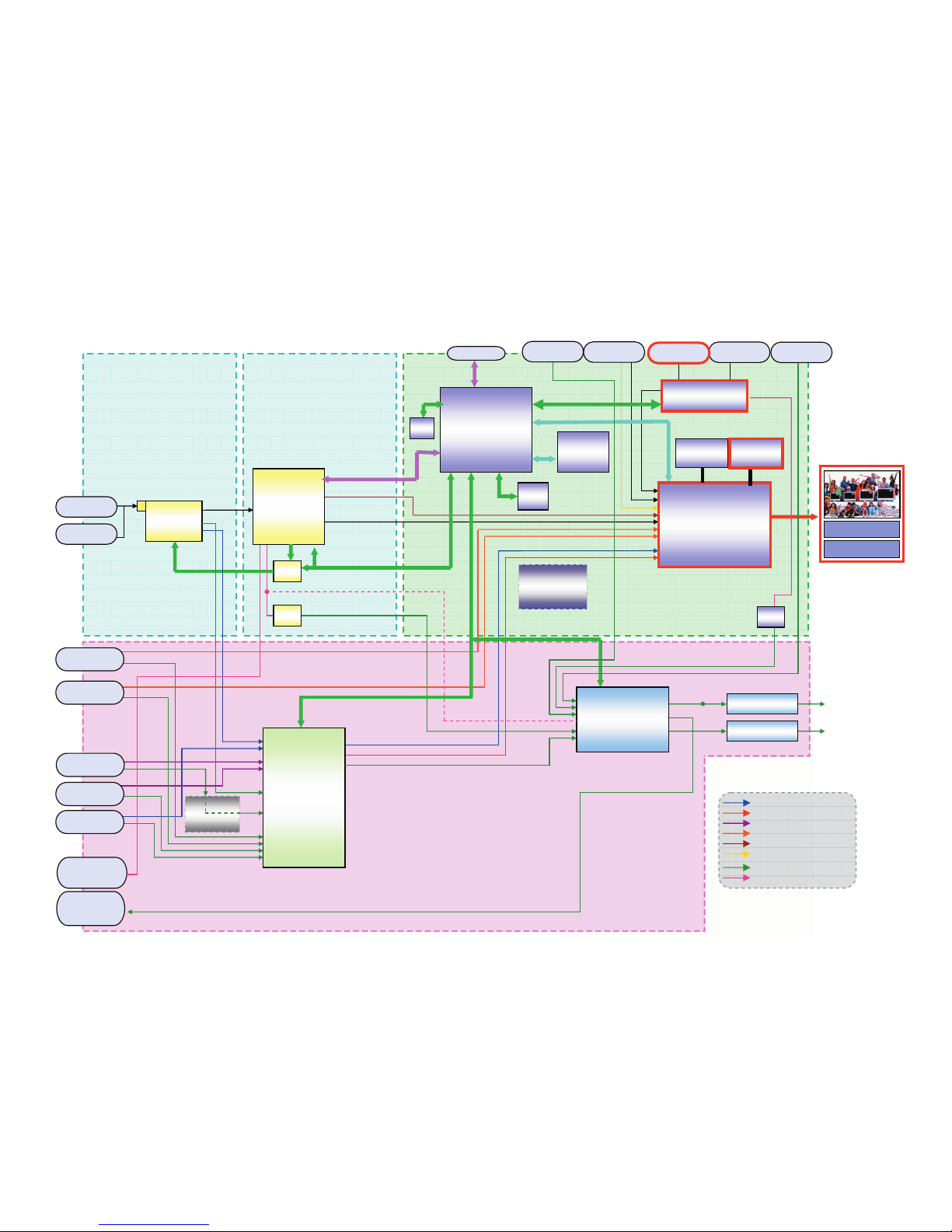
3-3. BLOCK DIAGRAM
2007/1/22
Analog-Component/RGB
Y/C
CVBS+Y/C
Digital-Component
Audio (Analog)
Audio (Digital)
CVBS
PC-RGB
Audio SW
CD4052
Digital F/E BU
RF
Hs/Vs
D-Comp[15:0]
UFE
UFE
Audio
for DVI
CLK/Hs/Vs
Auto Wide
CXD2057M
Main Micro
MB91305
EEP
Flash
2MByte
TMDS
I2C
8bit Multiplex BUS
HDMI
16bit
BUS
SPDIF
Cable
PC
I2C
Optical Audio
Out
SW
SW
I2S
Comp1
AV SW
CXA2069Q
Comp2
(S)Video1
(S)Video2
Video3
Audio out
(Fix/Var.)
Panel䋨FHD䋩
Backlight
Inverter
AV mo use
Audio Amp.
HP Amp.
HP Amp.
MAP4400A
D/A
MPEG DEC.
MPEG DEC.
CPU
CPU
ATi
ATi
x240H
x240H
I2C
IF
QT
QSF
D/A
D/A
AU/H
Chroma Dec/IP
/Scalar
Trident SVP-LXS
Audio
for PC
HDMI
UART
Jig(ECS)
HDMI-Rx
SiI9023
I2S
DDR1
4M x 32bit
DDR1
4M x 32bit
I2C
I2C
RTC
UART
☛
KDL-40V2500/46V2500/46V25L1
KDL-40V2500/46V2500/46V25L1 26
1 | 2 | 3 | 4 | 5 | 6 | 7 | 8 | 9 | 10 | 11 | 12 | 13 | 14 | 15 | 16 | 17 | 18 | 19 | 20 | 21 | 22 |
A
—
B
—
C
—
D
—
E
—
F
—
G
—
H
—
I
—
J
—
K
—
L
—
M
—
N
—
O
—
P
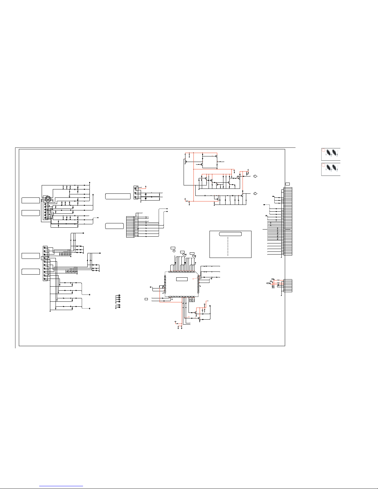
AU BOARD SCHEMATIC DIAGRAM (1 OF 2)
3-4. SCHEMATICS AND SUPPORTING INFORMATION
D1_IN_AU_L,D1_IN_AU_R
D2_IN_AU_L,D2_IN_AU_R
2012
16V
1
B
C9006
CHIP
0
R9013
1/10W
RN-CP
470k
R9004
CHIP
0
R9012
2012
16V
1
B
C9007
2012
16V
1
B
C9008
CHIP
0
R9010
1/10W
RN-CP
470k
R9005
1/10W
RN-CP
220k
R9088
CHIP
0
R9011
1/10W
RN-CP
220k
R9089
1/10W
RN-CP
470k
R9007
2012
16V
1
B
C9005
D1_IN_CB,D1_IN_CR,D1_IN_Y
D2_IN_CB,D2_IN_CR,D2_IN_Y
D3.3V
16V
100
C2015
V2_IN_AU_L,V2_IN_AU_R
16V
10
C2019
D1_IN_AU_L,D1_IN_AU_R
2012
16V
1
B
C2017
V2_IN_C,V2_IN_S2SW,V2_IN_SSW,V2_IN_V,V2_IN_Y
V1_IN_AU_L,V1_IN_AU_R
V3_IN_AU_L,V3_IN_AU_R
V1_IN_C,V1_IN_S2SW,V1_IN_SSW,V1_IN_V,V1_IN_Y
2012
16V
1
B
C2016
22uH
L2002
1608
16V
0.22
B
C2020
D2_IN_AU_L,D2_IN_AU_R
1/10W
RN-CP
22
R9038
1/10W
RN-CP
22
R9043
1/10W
RN-CP
22
R9044
1/10W
RN-CP
22
R9034
1/10W
RN-CP
22
R9036
1/10W
RN-CP
22
R9037
CHIP
0
R2017
A9V
GRN
BLU
RED
WHT
RED
GRN
BLU
RED
WHT
RED
J9002
1
2
3
4
5
6
7
8
9
10
11
12
13
14
15
16
17
18
19
20
CHIP
0
R9023
1/10W
RN-CP
100
R9078
2012
10V
2.2
B
C9020
2012
10V
2.2
B
C9019
2012
10V
2.2
B
C9021
1/10W
RN-CP
100
R9057
1/10W
RN-CP
470k
R9020
1/10W
RN-CP
100
R9061
1/10W
RN-CP
75
R9039
5%
1/10W
RN-CP
1k
R9060
1608
10V
0.47
B
C9016
2012
10V
2.2
B
C9022
2012
16V
1
B
C9023
2012
16V
1
B
C9015
2012
16V
1
B
C9024
2012
16V
1
B
C9014
V3_IN_AU_L,V3_IN_AU_R
1608
CHIP
R9045
0
1/10W
RN-CP
1k
R9059
1/10W
RN-CP
470k
R9021
CHIP
0
R9031
1/10W
RN-CP
100
R9058
V1_IN_AU_L,V1_IN_AU_R
CHIP
0
R9030
CHIP
0
R9024
1608
CHIP
R9046
0
1/10W
RN-CP
R9022
470k
1/10W
RN-CP
470k
R9019
34
12
J9001
12
34
56
7
8
9
10
11
13
12
14
15
16
17
18
19
20
V1_IN_C,V1_IN_S2SW,V1_IN_SSW,V1_IN_V,V1_IN_Y
1/10W
RN-CP
470k
R9006
1608
50V
4700p
B
C2114
2SC3052EF-T1-LEF
Q2109
1/10W
RN-CP
5%
4.7k
R2121
1608
16V
0.1
B
C2101
2012
6.3V
4.7
B
C2122
10uH
L2101
1608
CHIP
R2140
0
1608
16V
0.22
B
C2120
1/10W
RN-CP
5%
1k
R2137
2SA1235TP-1EF
Q2102
2SA1235TP-1EF
Q2104
1/10W
RN-CP
5%
4.7k
R2109
RB501V-40TE-17
D2101
16V
100
C2103
1/10W
RN-CP
5%
1M
R2117
1608
50V
2200p
B
C2119
2SA1235TP-1EF
Q2101
2SC3052EF-T1-LEF
Q2108
1608
25V
0.022
B
C2105
1/10W
RN-CP
5%
1M
R2132
1/10W
RN-CP
5%
2.2k
R2101
1608
16V
0.1
B
C2111
1/10W
RN-CP
0.5%
2.7k
R2125
1/10W
RN-CP
0.5%
3.9k
R2128
A9V
VD9025
VD9026
1/10W
RN-CP
1k
R9095
1/10W
RN-CP
1k
R9096
1/10W
RN-CP
1k
R9097
1/10W
RN-CP
1k
R9098
1/10W
RN-CP
1k
R9099
1/10W
RN-CP
1k
R9100
1/10W
RN-CP
1k
R9101
1/10W
RN-CP
1k
R9102
D3.3V
D5V
1
2
3
4
5
6
7
8
9
9P
CN9502
A9V
GND
D5V
D3.3V
GND
GND
Hsync_AU
Vsync_AU
GND
V2_IN_AU_L,V2_IN_AU_R
1
2
3
4
5
6
7
8
9
10
11
12
13
14
15
15P
CN9001
HP_DET
HP_OUT_AU_L
AU_IN_GND
HP_OUT_AU_R
V2_IN_SSW
V2_IN_S2SW
V2_IN_AU_R
AU_IN_GND
V2_IN_AU_L
GND
V2_IN_C
GND
V2_IN_Y
GND
V2_IN_V
V2_IN_C,V2_IN_S2SW,V2_IN_SSW,V2_IN_V,V2_IN_Y
A9V
1/10W
RN-CP
100
R2019
CHIP
0
R2027
A9V
10uH
L2003
SEL2_C,SEL2_Y/CV
1608
16V
0.22
B
C2021
CHIP
0
R2028
1/10W
RN-CP
470
R2037
16V
100
C2023
1/10W
RN-CP
470
R2038
2SC3052EF-T1-LEF
Q2002
2SC3052EF-T1-LEF
Q2001
1/10W
RN-CP
100
R2020
A9V_B
1608
1/10W
RN-CP
5%
4.7k
R2133
1608
1/10W
RN-CP
5%
4.7k
R2130
2SC3052EF-T1-LEF
Q2112
16V
47
C2117
10V
100
C2123
1608
25V
1000p
CH
C2124
1608
RN-CP
R2108
22k
1/10W
0.5%
2012
16V
2.2
C
C2109
2SC3052EF-T1-LEF
Q2105
2SA1235TP-1EF
Q2113
1608
16V
0.1
B
C2125
1608
RN-CP
R2123
1k
1/10W
5%
D3.3V
1608
1/10W
RN-CP
0.5%
R2114
56k
RN-CP
3.9k
R2129
1/10W
0.5%
0
R2134
2SC3052EF-T1-LEF
Q2107
1608
16V
B
C2126
0.1
2SC3052EF-T1-LEF
Q2111
16V
100
C2127
2012
16V
2.2
C
C2118
1/10W
RN-CP
0.5%
47k
R2107
CHIP
0
R9333
CHIP
0
R9334
R2039
CHIP
0
1608
25V
1000p
CH
C9501
1608
25V
1000p
CH
C9502
1608
RN-CP
R9506
1/10W
0.5%
39k
1608
16V
B
C2106
0.1
1M
R2151
100
R2152
12345678
910111213141516171819
20
21
22
23
24
25
26
27
28
29
30
31
32
3334353637383940414243
4445464748495051
52
53
54
55
56
57
58
59
60
61
62
63
64
CXA2069Q-TL
IC2001
V1
LV1Y1RV1
C1
S2-1
S-1
V2
LV2Y2RV2
C2
S2-2
S-2V3LV3Y3RV3
C3
S2-3
S-3
V4
LV4
Y4
RV4
C4
S2-4
S-4
LV5
V5
RV5
ADR
SCL
SDA
AGND
DCOUT
COUT3
LOUT3
YOUT3
ROUT3
VOUT3
VCC
LOUT2
V/YOUT2
ROUT2
TRAP2
COUT2
MUTE
YIN1
BIAS
CIN1
LOUT1
VOUT1
ROUT1
TRAP1
YOUT1
VGND
COUT1
LV6
V6
RV6
LTV
TV
RTV
CHIP
R9086
0
CHIP
0
R9150
CHIP
0
R9151
CHIP0
R9152
CHIP0
R9153
CHIP0
R9154
CHIP0
R9155
CHIP0
R9156
25V
1000p
CH
C9032
V_DET
V_AVSW
V3_IN_V
V_AVSW
M_HSYNC
HP_DET
SEL2_AU_L
V3_IN_V
SPDIF
SCL_B_5V
SEL2_AU_R
TV_L_UC
AUOUT_AU_L
HP_OUT_AU_R
AU_PRE_GND
TV_R_UC
SDA_B_5V
V_IN
AUOUT_AU_R
HP_OUT_AU_L
0
FB9003
CHIP
1/10W
RN-CP
220
R9008
0.5%
1/10W
RN-CP
220
R9009
0.5%
1/10W
RN-CP
220
R9014
0.5%
1/10W
RN-CP
220
R9015
0.5%
1/10W
RN-CP
220
R9016
0.5%
1/10W
RN-CP
220
R9017
0.5%
1/10W
RN-CP
220
R9018
0.5%
1/10W
RN-CP
220
R9025
0.5%
1/10W
RN-CP
220
R9026
0.5%
1/10W
RN-CP
220
R9027
0.5%
1/10W
RN-CP
220
R9028
0.5%
1/10W
RN-CP
220
R9029
0.5%
1/10W
RN-CP
220
R9032
0.5%
1/10W
RN-CP
220
R903
3
0.5%
1/10W
RN-CP
220
R9035
0.5%
1/10W
RN-CP
220
R9040
0.5%
1/10W
RN-CP
220
R9041
0.5%
1/10W
RN-CP
220
R9042
0.5%
1/10W
RN-CP
0.5%
220
R9062
1/10W
RN-CP
0.5%
220
R9063
1/10W
RN-CP
0.5%
220
R9064
1/10W
RN-CP
0.5%
220
R9065
1/10W
RN-CP
0.5%
220
R9066
1/10W
RN-CP
0.5%
220
R9067
1/10W
RN-CP
0.5%
220
R9068
1/10W
RN-CP
0.5%
220
R9069
1/10W
RN-CP
0.5%
220
R9070
CHIP
R2034
0
1/10W
100
R2030
1/10W
RN-CP
100
R2006
CHIP
0
R2015
1/10W
RN-CP
100
R2007
1/10W
RN-CP
1k
R2024
CHIP
0
R2033
1608
16V
0.22
B
C2018
1608
16V
0.22
B
C2013
2012
16V
1
B
C2025
1/10W
RN-CP
1k
R2023
2012
16V
1
B
C2024
2012
10V
2.2
B
C2026
CHIP
0
R2014
CHIP
0
R2103
1/10W
RN-CP
5%
R2139
330
1/10W
RN-CP
2.2k
R2104
0.5%
1/10W
RN-CP
100
R2102
5%
1/10W
RN-CP
5%
R2112
470
1/10W
RN-CP
5%
R2126
1k
1/10W
RN-CP
0.5%
10k
R2120
1608
16V
0.1
B
C2115
1608
25V
B
C2116
0.022
1/10W
RN-CP
5%
R2113
2.2k
V_DET
AC_OFF_DET_AU
SDA_B_5V
SCL_B_5V
REC_MUTE
SP_SD_MUTE
D2_IN_CB,D2_IN_CR,D2_IN_Y
LINE_MUTE
HP_DET
D1_IN_CB,D1_IN_CR,D1_IN_Y
HDMI_L
M_HSYNC
CHIP
0
R9159
PC_IN_R
CHIP
0
R9161
SEL2_C,SEL2_Y/CV
HDMI_R
DVI_L
PC_IN_L
SP_MUTE
DVI_R
CHIP0
R9501
AU_PROT
HP_MUTE
CHIP
0
R9160
RESET_AUDIO
AU_OPT_OUT_MUTE
CHIP
0
R9502
VIN
VCC
GND
J9003
1
2
3
4
5
6
7
8
9
10
11
12
13
14
15
16
17
18
19
20
21
22
23
24
25
26
27
28
29
30
31
32
33
34
35
36
37
38
39
40
41
42
43
44
48
47
45
46
49
49P
CN9501
WHT
PC_IN_R
GND
PC_IN_L
GND
DVI_R
GND
DVI_L
GND
HDMI_R
GND
HDMI_L
HP_DET
HP_MUTE
SP_SD_MUTE
SP_MUTE
RESET_AUDIO
AU_OPT_OUT_MUTE
LINE_MUTE
AC_OFF_DET_AU/TV_R_(AEP)
REC_MUTE/TV_L(AEP)
AU_PROT
SCL_B_5V
SDA_B_5V
M_HSYNC
V_DET
SEL2_C
GND
SEL2_Y/CV
GND
CR3
GND
CB3
GND
Y3
N.C./AVLINK(AEP)
N.C./FB_2
L3_2/MODE_2
CR2/R2
GND
CB2/B2
GND
Y2/G2
N.C./FB_1
L3_1/MODE_1
CR1/R1
GND
CB1/B1
GND
Y1/G1
1/10W
RN-CP
10k
R2008
1/10W
RN-CP
33k
R2009
CHIP
0
R9522
CHIP
0
R9529
CHIP
0
R9527
CHIP
0
R9530
CHIP
0
R9526
CHIP
0
R9524
CHIP
0
R9528
CHIP
0
R9523
CHIP
0
R9525
CHIP
0
R9515
CHIP
0
R9516
CHIP
0
R9517
CHIP
0
R9518
CHIP0
R9519
CHIP0
R9520
CHIP0
R9521
0uH
L9503
0uH
L9504
0uH
L9505
AU_GND
RN-CP
100
R9157
1/10W
RN-CP
100
R9158
1/10W
MA8100-TX
D9001
MA8100-TX
D9002
MA8100-TX
D9003
MA8100-TX
D9004
MA8100-TX
D9008
MA8100-TX
D9009
MA8100-TX
D9012
MA8100-TX
D9013
MA8100-TX
D9014
MA8100-TX
D9015
MA8100-TX
D9016
MA8100-TX
D9017
MA8100-TX
D9018
VD9001
MA8100-TX
VD9002
MA8100-TX
VD9003
MA8100-TX
VD9004
MA8100-TX
VD9005
MA8100-TX
VD9006
MA8100-TX
VD9007
MA8100-TX
VD9008
MA8100-TX
VD9009
MA8100-TX
VD9010
MA8100-TX
VD9011
MA8100-TX
VD9012
MA8100-TX
E
TERMINAL
CN9521
E
TERMINAL
CN9522
E
TERMINAL
CN9523
E
TERMINAL
CN9524
E
TERMINAL
CN9525
E
TERMINAL
CN9526
V1_IN_AU_L
V2_IN_S2SW
V2_IN_C
V2_IN_SSW
V2_IN_Y
D1_IN_AU_L
V2_IN_V
D1_IN_AU_R
V2_IN_AU_R
V3_IN_AU_R
V2_IN_AU_L
V3_IN_AU_L
V1_IN_AU_R
V1_IN_SSW
V1_IN_S2SW
V1_IN_C
V1_IN_Y
D2_IN_AU_R
D2_IN_AU_L
V1_IN_SSW
V1_IN_S2SW
V1_IN_C
V1_IN_Y
V1_IN_V
V1_IN_AU_L
V1_IN_AU_R
V3_IN_AU_L
V3_IN_AU_R
D2_IN_AU_R
D2_IN_AU_L
D1_IN_AU_R
D1_IN_AU_L
V2_IN_AU_R
SEL2_Y/CV
SEL2_C
D1_IN_Y
D1_IN_CB
D2_IN_Y
D2_IN_CB
D2_IN_CR
V2_IN_V
V1_IN_V
V2_IN_SSW
V2_IN_S2SW
V2_IN_AU_L
V2_IN_C
V2_IN_Y
SEL2_C
D1_IN_CB
D1_IN_Y
D2_IN_CR
D2_IN_CB
D2_IN_Y
D1_IN_CR
SEL2_Y/CV
D1_IN_CR
VideoInput3
VideoInput1
Opt/Audio Output
ComponentInput2
ComponentInput1
VideoInput2
Video2
Video1
IIC
AV SW
Video3
VideoSystem
TV: AnalogTuner
IN1: Video1
IN2: Video2
IN3: Video3
IN4: DigitalTuner
IN5:
IN6:
OUT1:
OUT2:C-Video
OUT3:VideoOutput
CXA2069Q I/O list
AudioSystem
TV: AnalogTuner
IN1: Video1
IN2: Video2
IN3: Video3
IN4:DigitalTuner(RECOUT)
IN5:Component1
IN6:Component2
OUT1:
OUT2: C-Video(to Trident)
OUT3:VideoOutput
I/O terminal
GNDterminal
B
D5V
D3.3V
A9V
B
TOB
AU MOUNT (1/2)
A/VSWITCH
INPUTS
4.4
4.4
5.0
4.4
4.4
5.0
4.4
4.5
3.9
4.4
4.4
4.5
4.3
4.4
4.2
4.4
4.4
4.4
4.4
4.4
4.4
3.9
4.2
3.9
4.4
4.4
4.4
4.4
0.1
4.9
4.4
3.9
4.4
4.4
0.1
0.1
4.4
3.9
4.4
3.9
1
2
4.4
3.6
3.7
4.3
2.6
2.0
1.9
1.2
1.4
2.0
1.3
2.7
3.2
2.7
1.8
-0.9
3.2
1.2
0.78.6 3.5
0.0
TOBUBOARD
CN4001
TOBUBOARD
CN7008
A-1184-344-A<WAX2F>AU-P1
TOH2BOARD
CN1201
1
Vp-p(H)
2
1.4 Vp-p (H)
AU BOARD WAVEFORMS
1.2
KDL-40V2500/46V2500/46V25L1
KDL-40V2500/46V2500/46V25L1 27
1 | 2 | 3 | 4 | 5 | 6 | 7 | 8 | 9 | 10 | 11 | 12 | 13 | 14 | 15 | 16 | 17 | 18 | 19 | 20 | 21 | 22 | 23
A
—
B
—
C
—
D
—
E
—
F
—
G
—
H
—
I
—
J
—
K
—
L
—
M
—
N
—
O
—
P
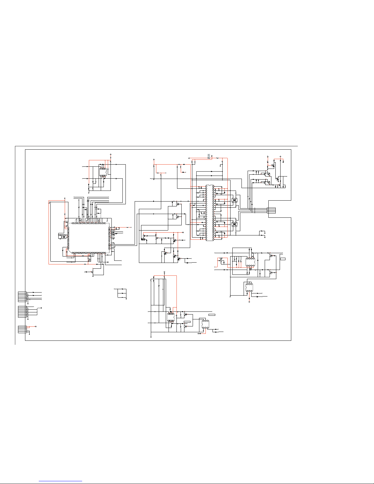
AU BOARD SCHEMATIC DIAGRAM (2 OF 2)
2012
16V
1
B
C2523
1/10W
RN-CP
10k
R2517
16V
10
C2809
RT1N441M-TP-1
Q2510
16V
10
C2590
AU_PRE_GND
2012
16V
1
B
C2536
16V
47
C2528
1/10W
RN-CP
47k
R2515
2012
16V
1
B
C2518
A9V
1/10W
RN-CP
47k
R2520
RT1N441M-TP-1
Q2519
RT1N441M-TP-1
Q2520
AU_PRE_GND
A9V
1/10W
RN-CP
0.5%
2.2k
R2616
1608
50V
2200p
B
C2547
1608
50V
2200p
B
C2548
16V
47
C2805
16V
47
C2511
16V
47
C2544
AU_PRE_GND
1/10W
RN-CP
0.5%
47k
R2832
CHIP
0
R2852
16V
10
C2800
AU_PRE_GND
2SA1235TP-1EF
Q2505
1608
25V
0.1
B
C2555
1608
50V
2200p
B
C2556
16V
10
C2534
16V
10
C2814
2012
16V
1
B
C2535
CHIP
0
R2636
1
2
3
4
4P
CN2500
L+
L-
R-
R+
8765
4321
NJM4558V-TE2
IC2503
AOUTPUT
A-IN
A+IN
GND B +IN
B-IN
BOUTPUT
VCC
1608
50V
2200p
B
C2550
1/10W
RN-CP
0.5%
47k
R2615
CHIP
0
R2622
1/10W
RN-CP
0.5%
47k
R2613
2012
16V
1
B
C2529
1/10W
RN-CP
0.5%
2.2k
R2834
16V
10
C2591
16V
10
C2811
CHIP
0
R2851
16V
10
C2519
16V
10
C2554
AU_PRE_GND
1608
25V
0.1
B
C2539
1608
50V
2200p
B
C2549
16V
10
C2538
16V
10
C2589
16V
47
C2573
2012
25V
1
C2621
1608
25V
0.1
B
C2530
AU_PRE_GND
2012
16V
1
B
C2537
AU_GND
CHIP
0
R2620
2012
25V
1
C2620
1608
50V
2200p
B
C2546
1608
25V
0.1
B
C2520
16V
10
C2813
1608
50V
2200p
B
C2545
RT1N441M-TP-1
Q2511
2012
16V
1
B
C2533
1/10W
RN-CP
47k
R2514
8765
4321
NJM3414AV(TE2)
IC2802
AOUTPUT
A-INPUT
A+INPUT
GNDB+INPUT
B-INPUT
BOUTPUT
VCC
16V
10
C2553
16V
47
C2557
1608
50V
2200p
B
C2542
2012
16V
1
B
C2521
1/10W
RN-CP
0.5%
2.2k
R2614
16V
47
C2817
2SC3052EF-T1-LEF
Q2502
CHIP
0
R2637
2012
25V
1
C2619
AU_PRE_GND
16V
47
C2818
2012
16V
1
B
C2527
1/10W
RN-CP
0.5%
47k
R2833
16V
10
C2588
18.432MHz
X2500
2SC3052EF-T1-LEF
Q2508
8765
4321
NJM4558V-TE2
IC2801
AOUTPUT
A-IN
A+IN
GND B +IN
B-IN
BOUTPUT
VCC
1/10W
RN-CP
0.5%
2.2k
R2835
10uH
L2505
D5V
DTV_IN
JL2503
A9V
AU_GND
AU_15V
2012
16V
1
B
C2803
2012
16V
1
B
C2804
1/10W
RN-CP
47k
R2805
1/10W
RN-CP
47k
R2806
0uH
FB2500
0uH
FB2501
0uH
FB2502
0uH
FB2503
A9V
1
2
3
4
5
6
7
7P
CN2301
TV_R/TV_V(GA)
GND
TV_L/QSS
GND
N.C./FM_AM
TV_V(UC)/GND
N.C.
1
2
3
4
5
6
7
8
8P
CN2302
SPDIF
GND
DATA0
GND
BCK
GND
LRCK
GND
DTV_IN
0
R2303
0
R2304
2SA1235TP-1EF
Q2514
2SA1235TP-1EF
Q2516
2SA1235TP-1EF
Q2515
2SA1235TP-1EF
Q2517
2SC3052EF-T1-LEF
Q2518
2012
16V
1
B
C2551
2012
16V
1
B
C2552
0uH
FB2504
0uH
FB2505
0uH
FB2506
0uH
FB2507
0uH
FB2508
1608
50V
470p
B
C2514
CHIP
0
R2876
CHIP
0
R2879
1
2
3
4
5
CN2303
5P
UNREG15V
UNREG15V
NC
AU_GND
AU_GND
RT1N141M-TP-1
Q2521
1/10W
RN-CP
6.8k
R2566
1/10W
RN-CP
10k
R2567
L2504
1608
25V
1000p
CH
C2561
1608
25V
1000p
CH
C2562
1608
25V
1000p
CH
C2563
1608
25V
1000p
CH
C2564
L2512
L2513
L2511
L2506
1608
25V
1000p
CH
C2565
1608
CHIP
R2882
0
1608
CHIP
R2883
0
1608
CHIP
R2884
0
L2502
PS2501
4A
25V
25V
470
C2613
35V
100
C2614
35V
100
C2615
35V
100
C2616
35V
100
C2617
L2508
22uH
12
RN-CP
4.7k
R2822
1/10W
0.5%
HP_OUT_AU_R
AU_+8V
PC_IN_L
SDA_B_5V
FIX/VAR_R_IN
009:4K
TV_L_UC
V_IN
AUOUT_AU_R
HDMI_R
AU_PRE_GND
AU_PROT
FIX/VAR_L_IN
HP_L_IN
FM/AM
RN-CP
4.7k
R2821
1/10W
0.5%
DVI_L
HP_R_IN
RN-CP
8.2k
R2562
1/10W
HP_OUT_AU_L
SCL_B_5V
RESET_AUDIO
SEL2_AU_L
HDMI_L
SEL2_AU_R
AU_PRE_GND
HP_L_IN
FIX/VAR_R_IN
TV_R_UC
HP_R_IN
AU_HP9V
PC_IN_R
RN-CP
8.2k
R2563
1/10W
SPDIF
DVI_R
AU_HP9V
SP_SD_MUTE
AUOUT_AU_L
FIX/VAR_L_IN
AC_OFF_DET_AU
AU_+8V
SP_MUTE
1608
50V
1500p
B
C2592
1608
50V
1500p
B
C2595
1608
50V
1500p
B
C2596
1608
50V
1500p
B
C2599
1608
50V
150p
CH
C2593
1608
50V
150p
CH
C2594
1608
50V
150p
CH
C2597
1608
50V
150p
CH
C2598
1/10W
RN-CP
0.5%
6.8k
R2624
1/10W
RN-CP
0.5%
6.8k
R2625
1/10W
RN-CP
0.5%
6.8k
R2630
1/10W
RN-CP
0.5%
6.8k
R2631
25V
0.22
C2583
B
2012
1/10W
RN-CP
1k
R2872
1/10W
RN-CP
220k
R2873
16V
470
C2826
DTC614TUT106
Q2806
DTC614TUT106
Q2807
1608
50V
100p
CH
C2815
0.1
C2604
25V
2012
B
1/10W
RN-CP
R2601
100k
1/10W
RN-CP
3.3k
R2829
1/10W
RN-CP
4.7k
R2801
1/10W
RN-CP
100k
R2839
16V
1
C2525
B
2012
1/10W
RN-CP
82k
R2831
1/10W
RN-CP
R2564
10k
1/10W
RN-CP
100k
R2827
1/10W
RN-CP
4.7k
R2802
1/10W
RN-CP
R2823
0.5%
10k
1/10W
RN-CP
10k
R2814
1.5p
C2505
1608
16V
0.1
B
C2812
1/10W
RN-CP
3.3k
R2830
1/10W
RN-CP
12k
R2815
1/10W
RN-CP
1M
R2587
25V
0.1
B
C2510
16V
1
C2524
B
2012
1.5p
C2504
CHIP
0
R2612
0.1
C2606
25V
B
2012
25V
1
C2575
1608
16V
0.1
B
C2801
1/10W
RN-CP
47k
R2611
1/10W
RN-CP
12k
R2539
0.5%
100k
R2511
1/10W
RN-CP
100k
R2826
1/10W
RN-CP
220
R2844
1608
50V
100p
CH
C2816
2012
25V
1
C2576
1/10W
RN-CP
10k
R2658
1608
16V
0.1
B
C2543
1/10W
RN-CP
100k
R2843
1/10W
RN-CP
15k
R2804
0.5%
2012
25V
1
C2586
0.1
C2600
25V
2012
B
2012
25V
1
C2587
1608
16V
0.1
B
C2802
1/10W
RN-CP
12k
R2803
0.5%
1/10W
RN-CP
22k
R2588
1/10W
RN-CP
15k
R2540
0.5%
1/10W
RN-CP
R2820
10k
1/10W
RN-CP
47k
R2554
0.1
C2607
25V
2012
B
1/10W
RN-CP
47k
R2593
1/10W
RN-CP
5.6k
R2603
0.1
C2608
25V
2012
B
1/10W
RN-CP
82k
R2828
0.1C2603
25V 2012B
RN-CP
10k
R2617
1/10W
0.1
C2601
25V
2012
B
0.1
C2605
25V
B
1/10W
RN-CP
R2561
10k
1608
16V
0.1
B
C2810
1/10W
RN-CP
220
R2846
0.1C2602
25V
2012
B
1/10W
RN-CP
100k
R2645
1/10W
RN-CP
100k
R2647
1/10W
RN-CP
100k
R2644
1/10W
RN-CP
47k
R2656
1/10W
RN-CP
100k
R2642
2012
25V
1
B
C2627
1/10W
RN-CP
10k
R2652
CHIP
0
R2655
2012
25V
1
B
C2628
1608
16V
0.1
B
C2648
1/10W
RN-CP
100k
R2643
1/10W
RN-CP
100k
R2646
1/10W
RN-CP
100k
R2654
1/10W
RN-CP
100k
R2653
2012
25V
1
B
C2647
CHIP
0
R2662
CHIP
0
R2663
CHIP
0
R2664
CHIP
0
R2665
CHIP
0
R2855
CHIP
0
R2856
1005
50V
220p
B
C2515
1608
25V
0.1
B
C2540
1005
50V
1000p
CH
C2560
CHIP
0
R2512
RN-CP
4.7k
R2531
1/16W
0.5%
R2532
15k
1/16W
RN-CP
4.7k
R2533
1/16W
0.5%
RN-CP
R2534
15k
1/16W
0.5%
1/16W
RN-CP
100k
R2535
RN-CP
10k
R2537
1/16W
RN-CP
10k
R2541
1/16W
RN-CP
10k
R2545
1/16W
RN-CP
10k
R2547
1/16W
1/16W
RN-CP
47k
R2549
RN-CP
4.7k
R2550
1/16W
0.5%
1/16W
RN-CP
100k
R2555
RN-CP
4.7k
R2556
1/16W
0.5%
RN-CP
15k
R2557
1/16W
RN-CP
15k
R2559
1/16W
CHIP
0
R2525
R2301
0uH
2012
25V
1
C2618
RN-CP
10k
R2859
1/10W
CHIP
0
R2840
HP_MUTE
25V
C2819
B
1608
0.1
AC_OFF_DET_AU
1/10W
RN-CP
1M
R2837
RN-CP
10k
R2863
1/10W
AC_OFF_DET_AU
LINE_MUTE
1/10W
RN-CP
1M
R2858
RB160M-60TR
D2509
RB160M-60TR
D2514
RB160M-60TR
D2515
RB160M-60TR
D2510
RB160M-60TR
D2516
RB160M-60TR
D2511
RB160M-60TR
D2517
MC2836
D2504
CHIP
0
R2505
CHIP
0
R2504
2SC4154TP-1G
Q2815
RT1N141M-TP-1
Q2507
123
456
RT8H225C
IC2803
123
456
RT8H225C
IC2804
1/10W
RN-CP
0.5%
15k
R2626
1/10W
RN-CP
0.5%
15k
R2629
1/10W
RN-CP
0.5%
120k
R2632
1/10W
RN-CP
0.5%
120k
R2633
1/10W RN-CP
120k
R2627
1/10W
RN-CP
0.5%
39k
R2628
1
23
4
22uH
L2509
1
23
4
22uH
L2510
25V
0.68
C2623
B
3216
25V
0.68
C2624
B
3216
25V
0.68
C2625
B
3216
25V
0.68
C2626
B
3216
MA111-TX
D2505
MA111-TX
D2507
MA111-TX
D2513
MA111-TX
D2804
MA111-TX
D2805
MA8110-TX
D2501
15V
DTC614TUT106
Q2512
DTC614TUT106
Q2513
CHIP
0
R2841
DTC614TUT106
Q2803
DTC614TUT106
Q2804
15V
15V
0uH
R2518
0uH
R2519
15V
15V
AU_15V
4849505152
54321
4147 46 45 44 43 42
1211109876
34353637383940
19181716151413
27282930313233
20 21 22 23 24 25
26
R2A15105SP
IC2507
DVDD1
DGND1
PWM2A1
PWM1A1
PWM1B1
PWM2B1
OP1O
IN1
STBY/MUTE
MUTEC
SUB
VCOR
AGND
VREF
AVCC
SUB
CLK
CLKCTRL
IN2
OP2O
PWM2B2
PWM1B2
PWM1A2
PWM2A2
DGND2
DVDD2 HBA2
VDA2
VSA2
VSA2
OUTA2
OUTA2
VDB2
VSB2
VSB2
OUTB2
SUB
OUTB2
HBB2
HBB1
OUTB1
SUB
OUTB1
VSB1
VSB1
VDB1
OUTA1
OUTA1
VSA1
VSA1
VDA1
HBA1
1
2
34
5
6
7
8
9
10
11
12
13
14
15
16
17
1
8
1
9
2
0
2
1
2
223
24
25
26
27
28
29
30
31
32
33
34
3
5
36
37
38
39
40
4
14
2
43
44
45
46
47
4
84
95
05
1
5
25
35
45
55
6
57
58
59
60
61
62
63
64
65
66
67
6
8
6
9
70
71
72
73
74
75
76
77
78
7
9
80
MAP4400A-QA-B2-501-T
IC2501
NC
I2C_CL
I2C_DA
I2S_CL
I2S_WS
I2S_DATA_OUT
I2S_DA_IN1
I2S_DEL_IN
I2S_DEL_OUT
I2S_DEL_WS
I2S_DEL_WS
DVSUP
DVSUP
DVSS
DVSS
DVSS
I2S_DA_IN2NCI2S_CL3
I2S_WS3
RESETQ
I2S_DA_IN3
I2S_DA_IN4
DACA_R
DACA_L
VREF2
DACM_R
DACM_L
DACM_C
DACM_SUB
DACM_SR
DACM_SL
SC2_OUT_R
SC2_OUT_L
VREF1
SC1_OUT_R
SC1_OUT_L
CAPL_A
AHVSUP
CAPL_M
SC3_OUT_R
SC3_OUOT_L
AHVSS
AHVSS
AGNDC
NC
SC4_IN_L
SC4_IN_R
ASG
SC3_IN_L
SC3_IN_R
ASG
SC2_IN_L
SC2_IN_R
ASG
SC1_IN_L
SC1_IN_R
VREFTOP
SC5_IN_L
SC5_IN_R
AVSS
AVSS
NC
NC
AVSUP
AVSUP
ANA_IN1+
ANA_IN-
ANA_IN2+
TESTEN
XTAL_IN
XTAL_OUT
TP
AUD_CL_OUT
NC
SPDIF_OUT
D_CTR_I/O_1
D_CTR_I/O_0
ADR_SEL
STANDBYQ
RB160M-60TR
D2512
HDMI_R
HDMI_L
BCLK
LRCLK
AU_DATA
AU_DATA
BCLK
LRCLK
LINE_OUT
HP_OUT
A9V
TODETECT
LINE_OUT
AUDIO
AU MOUNT (2/2)
CN7803
TOQTBOARD
CN6200
TOG2ABOARD
TOSpeakers
OPAMP
5.0
5.0
5.0
5.0
5.0
5.0
0.0
0.0
0.0
0.0
AUDIODSP
0.0
2.4
2.3
3.8
3.7
3.8
3.8
4.4
3.8
3.8
3.8
3.8
3.8
3.8
0.0
3.8
0.
0
7.
3
3.8
3.8
0.0
3.8
7.4
0.0
4.6
5.0
5.0
1.7 1.74.6 0.0
0.
0
OPAMP
5.0
5.0
5.0
5.0
5.0
5.0
DIGITALAUDIOAMP
4.5
4.5
0.0
4.5
4.5
4.5
4.5
4.5
8.8
4.5
0.8.
4.5
4.5
4.5
7.2
15.5
7.2
15.5
7.2
15.5
7.2
15.5
7.2
0.0
0.0
0.0
0.0
MUTE
MUTE
0.0
2.8
0.014.3
2.8
MUTE
MUTE
MUTE
8.8
0.0
2.8
0.0
0.0
MUTE
MUTE
MUTE
5.0
5.0
5.0
5.05.0 5.0
0.0
0.0
0.0
0.0
7.2
7.2
0.0
7.1
0.0
7.1
0.0
2.9
A-1184-344-A<WAX2F>AU-P2
MUTE
MUTE
CN7314
TOQSFBOARD
 Loading...