

Page 1
HISTORY INFORMATION FOR THE FOLLOWING MANUAL:
Self Diagnosis
Supported model
SERVICE MANUAL
CONFIDENTIAL
ELECTRICAL SERVICE MANUAL
INTERNAL ONLY
ORIGINAL MANUAL ISSUE DATE: 3/2012
REVISION DATE SUBJECT
3/29/2012 Original Manual Release Date
AZ3TK
CHASSIS
LEVEL
CONFIDENTIAL
3
9-883-885-51
LCD DIGITAL COLOR TV
Page 2

LEVEL
CONFIDENTIAL
3
SERVICE MANUAL
MODEL COMMANDER DESTINATION
KDL-32BX355 RM-YD081 BRAZIL
KDL-40BX455 RM-YD081 BRAZIL
KDL-46BX455 RM-YD081 BRAZIL
AZ3TK
CHASSIS
9-883-885-51
LCD DIGITAL COLOR TV
Page 3

AZ3TK
TABLE OF CONTENTS
SECTION TITLE PAGE
Cautions and Warnings ....................................................................................................................................................................................................4
Safety Check-Out...............................................................................................................................................................................................................6
SECTION 1: DIAGRAMS
1-1. Printed Circuit Boards and Schematic Diagrams Information ............................................................................................................................8
1-2. Block Diagram ....................................................................................................................................................................................................9
1-3. Connector Diagrams ........................................................................................................................................................................................10
A Board Schematic
G Board Schematic
H Board Schematic
SECTION 2: ELECTRICAL PARTS LIST
KDL-32BX355
KDL-40BX455/46BX455
APPENDIX A: ENCRYPTION KEY COMPONENTS
...................................................................................................................................................................................................8
...........................................................................................................................................................................................11
..........................................................................................................................................................................................28
..........................................................................................................................................................................................29
........................................................................................................................................................................31
..................................................................................................................................................................................................31
..................................................................................................................................................................................31
.....................................................................................................................................................A-1
AZ3TK 3
Page 4

AZ3TK
CAUTIONS AND WARNINGS
CAUTION
These servicing instructions are for use by qualied service personnel only. To reduce the risk of electric shock, do not
perform any servicing other than that contained in the operating instructions unless you are qualied to do so.
WARNING!!
An isolation transformer should be used during any service to avoid possible shock hazard, in case of live chassis.
!
SAFETY-RELATED COMPONENT WARNING!!
There are critical components used in LCD color TVs that are important for safety. These components are identied with
shading and
with the part number specied in the parts list to prevent electric shock, re, or other hazard.
NOTE: Do not modify the original design without obtaining written permission from the manufacturer or you will void the
original parts and labor warranty.
!
mark on the schematic diagrams and the parts list. It is essential that these critical parts be replaced only
AZ3TK 4
Page 5
AZ3TK
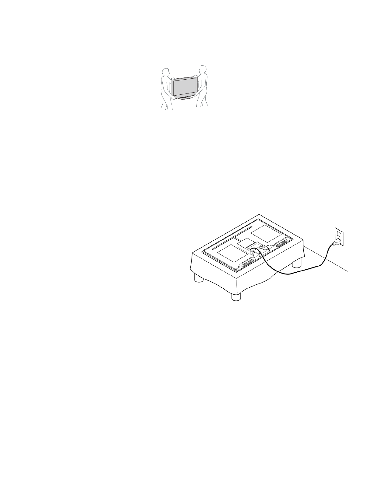
SETTING UP AND CARRYING THE TV
• Disconnect all cables when carrying the TV.
• Carry the TV with the adequate number of people; larger size TVs require two or more people.
• Correct hand placement while carrying the TV is very important for safety and to avoid damage.
USE CAUTION WHEN HANDLING THE LCD PANEL
When repairing the LCD panel, be sure you are grounded by using a wrist band.
When installing the LCD panel on a wall, the LCD panel must be secured using the 4 mounting holes on the rear
cover.
To avoid damaging the LCD panel:
1. Do not press on the panel or frame edge to avoid the risk of electric shock.
2. Do not scratch or press on the panel with any sharp objects.
3. Do not leave the module in high temperatures or in areas of high humidity for an extended period of time.
4. Do not expose the LCD panel to direct sunlight.
5. Avoid contact with water. It may cause a short circuit within the module.
6. Disconnect the AC power when replacing the backlight (CCFL) or inverter circuit.
(High voltage occurs at the inverter circuit at 650Vrms.)
7. Always clean the LCD panel with a soft cloth material.
8. Use care when handling the wires or connectors of
the inverter circuit. Damaging the wires may cause a
short.
9. Protect the panel from ESD to avoid damaging the
electronic circuit (C-MOS).
10. During the repair, DO NOT leave the Power On for
more than 1 hour while the TV is face down on a
cloth.
CLEANING THE LCD PANEL
CAUTION: When cleaning the TV, be sure to unplug the power cord to avoid any chance of electric shock.
Clean the cabinet of the TV with a dry soft cloth.
Wipe the LCD screen gently with a soft cloth.
; Stubborn stains may be removed with a cloth slightly moistened with a solution of mild soap and warm water.
; If using a chemically pretreated cloth, please follow the instruction provided on the package.
; Never use strong solvents such as a thinner, alcohol or benzine for cleaning.
; Periodic vacuuming of the ventilation openings is recommended to ensure proper ventilation.
; Do Not use paper towels, any type of abrasive pad, rags, rubber or vinyl materials to clean the screen. Using
these materials could easily scratch the screen which may result in permanent damage.
; Do Not use any cleaning product containing alkaline/acid cleaner, scouring powder, or volatile solvent, such as
alcohol, ammonia, benzine, thinner or insecticide. Using any of these harsh cleaners may result in permanent
damage to the screen.
; Do Not spray water or detergent directly onto the TV screen . If liquid drips into the bottom of the screen it may
cause a failure.
AZ3TK 5
Page 6
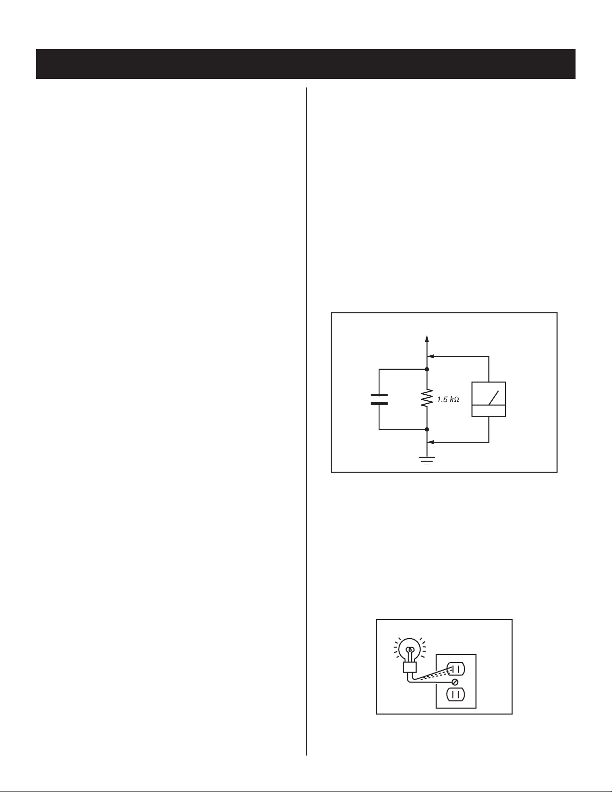
SAFETY CHECK-OUT
To Exposed Metal
Parts on Set
0.15 µF
Earth Ground
AC
Voltmeter
(0.75V)
AZ3TK
After correcting the original service problem, perform the
following safety checks before releasing the set to the
customer:
1. Check the area of your repair for unsoldered or
poorly soldered connections. Check the entire
board surface for solder splashes and bridges.
2. Check the interboard wiring to ensure that no
wires are “pinched” or touching high-wattage
resistors.
3. Check that all control knobs, shields, covers,
ground straps, and mounting hardware have been
replaced. Be absolutely certain that you have
replaced all the insulators.
4. Look for unauthorized replacement parts,
particularly transistors, that were installed during
a previous repair. Point them out to the customer
and recommend their replacement.
5. Look for parts which, though functioning, show
obvious signs of deterioration. Point them out to
the customer and recommend their replacement.
6. Check the line cords for cracks and abrasion.
Recommend the replacement of any such line
cord to the customer.
7. Check the antenna terminals, metal trim,
“metallized” knobs, screws, and all other exposed
metal parts for AC leakage. Check leakage as
described in “Leakage Test”.
LEAKAGE TEST
The AC leakage from any exposed metal part to earth
ground and from all exposed metal parts to any exposed
metal part having a return to chassis, must not exceed
0.5 mA (500 microamperes). Leakage current can be
measured by any one of three methods.
1. A commercial leakage tester. Follow the
manufacturers’ instructions provided with the
tester.
2. A battery-operated AC milliammeter.
3. Measuring the voltage drop across a resistor
by means of a VOM or battery-operated AC
voltmeter. The “limit” indication is 0.75 V, so
analog meters must have an accurate low
voltage scale. Nearly all battery-operated digital
multimeters that have a 2 VAC range are suitable.
(see Figure A)
Figure A. Use an AC voltmeter to check AC leakage.
HOW TO FIND A GOOD EARTH GROUND
The cover-plate retaining screw on most AC outlet boxes
is at earth ground. Verify the AC outlet box retaining screw
ground by connecting a 60W to 100W incandescent
(not a neon or uorescent lamp) between the hot side
of the receptacle and the retaining screw. Try both slots,
if necessary, to locate the hot side on the line; the lamp
should light at normal brilliance if the screw is at ground
potential. (see Figure B)
AZ3TK 6
Trouble Light
AC Outlet Box
Figure B. Checking for earth ground.
Page 7
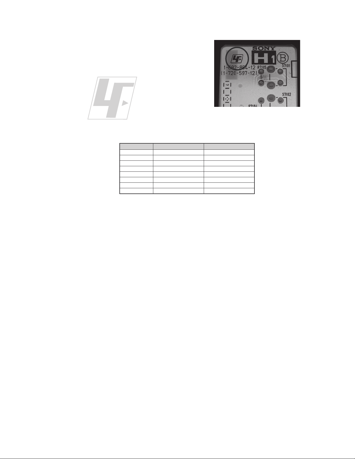
Th
e circuit boards used in these models have been processed using
Lead Free Solder. The boards are identified by the LF logo located
close to the board designation e.g. H1 etc [ see example ]. The
servicing of these boards requires special precautions to be taken as
outlined below.
example
It is strongly recommended to use Lead Free Solder material in order to guarantee optimal quality of new solder joints.
Lead Free Solder is available under the following part numbers :
rebmuntraP retemaiD skrameR
91-500-046-7mm3.0gK52.0
02-500-046-7mm4.0gK05.0
12-500-046-7mm5.0gK05.0
22-500-046-7mm6.0gK52.0
32-500-046-7mm8.0gK00.1
42-500-046-7mm0.1gK00.1
52-500-046-7mm2.1gK00.1
62-500-046-7mm6.1gK00.1
AZ3TK
Due to the higher melting point of Lead Free Solder the soldering iron tip temperature needs to be set to 370 degrees celsius.
This requires soldering equipment capable of accurate temperature control coupled with a good heat recovery characteristics.
AZ3TK 7
Page 8
AZ3TK
SECTION 1: DIAGRAMS
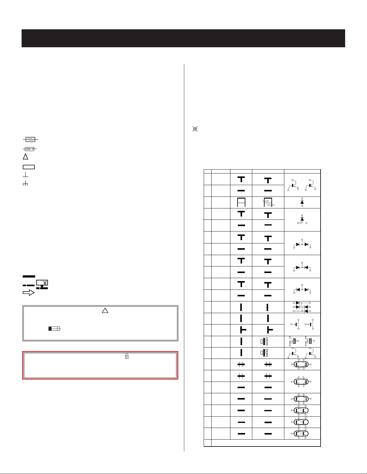
1-1. PRINTED CIRCUIT BOARDS AND SCHEMATIC DIAGRAMS INFORMATION
REFERENCE INFORMATION
All capacitors are in µF unless otherwise noted. pF : µµF 50WV or
less are not indicated except for electrolytics and tantalums.
All electrolytics are in 50V unless otherwise specied.
All resistors are in ohms. kΩ=1000Ω, MΩ=1000kΩ
Indication of resistance, which does not have one for rating
electrical power, is as follows: Pitch : 5mm
Rating electrical power :
1
/4 W in resistance, 1/
W and 1/
10
W in chip resistance.
16
1
/4 W
: nonammable resistor
: fusible resistor
: internal component
: panel designation and adjustment for repair
: earth ground
RESISTOR
: RN METAL FILM
: RC SOLID
: FPRD NONFLAMMABLE CARBON
: FUSE NONFLAMMABLE FUSIBLE
: RW NONFLAMMABLE WIREWOUND
: RS NONFLAMMABLE METAL OXIDE
: RB NONFLAMMABLE CEMENT
: ADJUSTMENT RESISTOR
COIL
: LF-8L MICRO INDUCTOR
Terminal name of semiconductors in silk screen
printed circuit ( )
Device Printed symbol Terminal name
Transistor
1
*
: earth-chassis
Transistor
2
All variable and adjustable resistors have characteristic curve B, unless
3
Diode
Cathode
otherwise noted.
Readings are taken with a color-bar signal input.
Readings are taken with a 10MΩ digital multimeter.
Voltages are DC with respect to ground unless otherwise noted.
Voltage variations may be noted due to normal production
tolerances.
All voltages are in V.
S : Measurement impossibility.
: B+line.
: B-line. (Actual measured value may be different).
: signal path. (RF)
Circled numbers are waveform references.
The components identied by shading and
only with part number specied.
The symbol indicates a fast-blow fuse and is displayed on the component
side of the board. Replace only with fuse of the same rating as marked.
NOTE: The components identied by a red outline and a mark contain condential
information. Specic instructions must be adhered to whenever these components
are repaired and/or replaced.
See Appendix A: Encryption Key Components in the back of this manual.
!
symbol are critical for safety. Replace
Diode
Diode
5
Diode
6
Diode
7
8
Diode
Diode
9
Diode
10
Diode
11
Diode
12
Transistor
13
(FET)
Transistor
14
(FET)
Transistor
15
(FET)
Transistor
16
Transistor
17
Transistor
18
Transistor
19
Transistor
20
Transistor
21
Transistor
22
Transistor
23
Discrete semiconductor
–
(Chip semiconductors that are not actually used are included.)
Anode
Anode
Anode
Anode Cathode
Anode
Anode Anode
Cathode
Cathode
Anode
Anode
Cathode
4
AZ3TK 8
CAPACITOR
: TA TANTALUM
: PS STYROL
: PP POLYPROPYLENE
: PT MYLAR
: MPS METALIZED POLYESTER
: MPP METALIZED POLYPROPYLENE
: ALB BIPOLAR
: ALT HIGH TEMPERATURE
: ALR HIGH RIPPLE
Collector
Base
Collector
Base
Cathode
Cathode
Common
Common
Common
Common
Common
Common
Drain
Drain
C1
E1
C1
E2
C2
B1
E2
C2
Emitter
Emitter
(NC)
(NC)
Cathode
Anode
Cathode
Cathode
Cathode
Anode
Anode
Source
Gate
Source
Gate
Source
Drain
Gate
Emitter
Collector
Base
B1 E1C2
B2 C1E2
B2 E2
B1 C2
B2 E2C1
B1 C2E1
B2 E2
B1 C2E1
B1 E1
C1(B2)
(B2)
E1
E2
C2C1
(B2)
E1
B1
C1
Anode
Circuit
D
G
D
S
B1
B1
B1
B1
B1
B1
D
G
S
S
D
G
S
C2B2C1
E1
E2
C2B2C1
E1
E2
E2B2E1
C1
C2
C2C1(B2)
E2
E2
E2E1(B2)
C1
C2
C2E1(B2)
C1
C2
Ver.1.6
G
Page 9
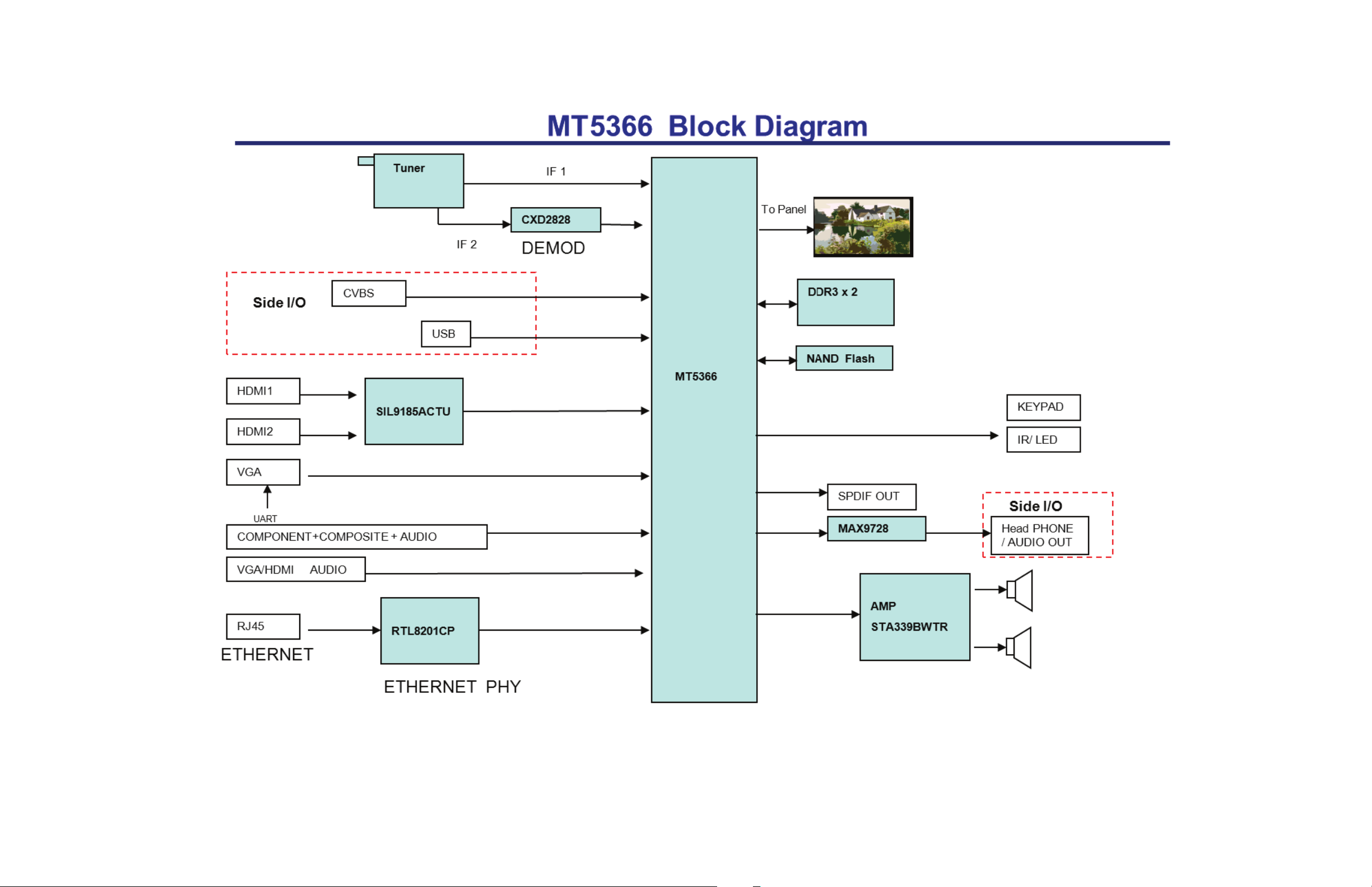
1-2. BLOCK DIAGRAM
AZ3TK
AZ3TK 9
Page 10
1-3. CONNECTOR DIAGRAMS
Panel
AZ3TK
AC
CN4001
CN201
CN4002
CN4003
CN8001
Main board
Power Board
TCON Board
Key Pad board
IR board
AZ3TK 10
Page 11

A BOARD SCHEMATIC
A
A
B
B
C
C
D
D
E
E
4
4
3
3
2
2
1 1
OPWRSB
BL_DIMMING
BL_ON/OFF
AC_DET
BL_DIMMING
OPWRSB
AC_DET#
INVERTER_DET#
BRIGHT_ADJAC_DET
BL_ON/OFF INVERTER_ON_OFF
BRIGHT_ADJ
INVERTER_ON_OFF
24V
STANDBY_CON
AC_DET#
INVERTER_DET#
3V3SB
AVDD3V3
+5VSB
+5V_SW
+5VSB
VCCK
AVDD3V3
DVDD3V3
VCCK
+12V
3V3SB
+5VSB
AVDD1V2
AVDD3V3
+5V_SW
+5V_SW
3V3SB
VCCK
+5VSB
+24V
DVDD3V3
24V
AVDD1V2
+5VSB
+24V
+12V
OPWRSB9
BL_DIMMING13
BL_ON/OFF13
AC_DET10,13
DVDD3V35,8,9,13,17
3V3SB6,7,9,13
GND3,4,5,6,7,8,9,10,11,12,13,14,16,17
VCCK9,13
AVDD3V34,7,10,11,12,13,14
AVDD1V27,8,9,12,14
+12V14
+5VSB4,5,6,9
+5V_SW5,7,10,12,13,14,16
+24V11
24V13
INVERTER_DET#13
AC_DET 10,13
STANDBY 13
OEM MODEL
Size
Rev
Date
Sheet
of
TPV MODEL
PCB NAME
T P V ( Top Victory Electronics Co . , Ltd. )
Key Component
絬 隔 瓜 絪 腹
FNNSAASN2AC23E
BDBT
1 16Wednesday, December 07, 2011
715G5177-M0D-000-004K
SYSTEM POWER
G5177-M0F-000-004K-1-111114
OEM MODEL
Size
Rev
Date
Sheet
of
TPV MODEL
PCB NAME
T P V ( Top Victory Electronics Co . , Ltd. )
Key Component
絬 隔 瓜 絪 腹
FNNSAASN2AC23E
BDBT
Wednesday, December 07, 2011
715G5177-M0D-000-004K
SYSTEM POWER
G5177-M0F-000-004K-1-111114
OEM MODEL
Size
Rev
Date
Sheet
of
TPV MODEL
PCB NAME
T P V ( Top Victory Electronics Co . , Ltd. )
Key Component
絬 隔 瓜 絪 腹
FNNSAASN2AC23E
BDBT
Wednesday, December 07, 2011
715G5177-M0D-000-004K
SYSTEM POWER
G5177-M0F-000-004K-1-111114
Control Interface
+5V Switch
Detection
INVERTER ON/OFF
H: OFF
L: ON
INVERTER ON/OFF
1.2 x (1+ 0/110) = 1.2V
Bright_Adj
Max:3.3V
Min: 0V
BRIGHT ADJUST
AC Detect
R2
Vout = 0.9x(R1+R2)/R2
R1
MAIN POWER
HI = > POWER_ON
LO = > POWER_OFF
1.149V
MTK
R713
13K OHM +-1%
R713
13K OHM +-1%
CN701
CONN
CN701
CONN
1
2
3
4
5
6
7
8
9
10
11
12
13
14
+
C709
100uF16V
+
C709
100uF16V
+
C704
220uF/16V
+
C704
220uF/16V
R706
100K 1/16W 5%
R706
100K 1/16W 5%
+
C719
100uF16V
+
C719
100uF16V
FB701
120R/6000mA
FB701
120R/6000mA
1
2
U702
G1117-33T63Uf
U702
G1117-33T63Uf
VI
3
VO
2
GND14
4
+
C728
100uF16V
+
C728
100uF16V
Q703
BC847C
Q703
BC847C
F700
5A 32V
F700
5A 32V
C713
100NF
C713
100NF
R704
51K 1/16W 5%
R704
51K 1/16W 5%
R707
2K7 1/16W 5%
R707
2K7 1/16W 5%
C708
10UF 10V
C708
10UF 10V
FB704
120R/6000mA
FB704
120R/6000mA
1 2
C721
3.3nF 50V
C721
3.3nF 50V
R712
3.6K 1%
R712
3.6K 1%
R730
4K7 1/16W 5%
R730
4K7 1/16W 5%
R726
10K 1/16W 5%
R726
10K 1/16W 5%
R714
9K1 1/16W 5%
R714
9K1 1/16W 5%
U703
BD9329EFJ
U703
BD9329EFJ
BST
1
VIN
2
SW
3
GND
4
FB
5
COMP
6
EN
7
SS
8
E-Pad
9
C725
NC/10uF 10V
C725
NC/10uF 10V
R70322K 1/16W 5% R70322K 1/16W 5%
C714
22N 25V
C714
22N 25V
C715
100NF
C715
100NF
Q702
AON4421
Q702
AON4421
D1D2D3G
4
S
5
D6D7D
8
R701
100R 1/16W 5%
R701
100R 1/16W 5%
C726
NC/22UF
C726
NC/22UF
C702
1UF 10V
C702
1UF 10V
R732
0R05 1/4W
R732
0R05 1/4W
R705
1K 1/16W 5%
R705
1K 1/16W 5%
C711
1uF 16V
C711
1uF 16V
R728
100R 1/16W 5%
R728
100R 1/16W 5%
R727
100R 1/16W 5%
R727
100R 1/16W 5%
L701 6.8uH
L701 6.8uH
R715
1K 1/16W 5%
R715
1K 1/16W 5%
R725
10K 1/16W 5%
R725
10K 1/16W 5%
+
C710
100uF16V
+
C710
100uF16V
R729
68K 1/16W 1%
R729
68K 1/16W 1%
C720
1UF 10V
C720
1UF 10V
U705U705
VI
3
VO
2
GND
1
4
4
C727
1UF 10V
C727
1UF 10V
U701
G1084-33TU3Uf
U701
G1084-33TU3Uf
VIN
3
VOUT
2
GND
1
C705
1UF 10V
C705
1UF 10V
+
C718
220uF/16V
+
C718
220uF/16V
C701
100NF
C701
100NF
A-Board
A BOARD SCHEMATIC DIAGRAM (1 OF 16)
AZ3TK
AZ3TK 11
Page 12

A BOARD SCHEMATIC DIAGRAM (2 OF 16)
5
5
4
4
3
3
2
2
1
1
D
D
C
C
B
B
A A
VGA_R_In
VGA_L_In
VSYNC#
VGASCL
VSYNC#
HSYNC#
VGASDA
HSYNC#
VGA11
GRN
VSYNC
HSYNC
RP
BP
SOG
VGACOM
GP
GRN
BLU
BLU
RED
RED
VGA_L_In
VGA_R_In
VGASCL
VGASDA
U0TX
U0RX
U0RX
G_G
VGA_Audio_L_In
VGA_Audio_R_In
VSYNC
HSYNC
BP
SOG
GP
VGACOM
RP
G_G
VGA_5V
U0TX
VGA_5V
VGA_5V
VGA11
VGASDA
VGASCL
+5VSB
VGA_L_In12
VGA_R_In12
VSYNC12
HSYNC12
BP12
SOG12
GP12
VGACOM12
RP12
VGASCL12
VGASDA12
U0TX9
U0RX9
+5VSB2,4,5,6,9
GND2,4,5,6,7,8,9,10,11,12,13,14,16,17
OEM MODEL
Size
Rev
Date
Sheet
of
TPV MODEL
PCB NAME
T P V ( Top Victory Electronics Co . , Ltd. )
Key Component
絬 隔 瓜 絪 腹
FNNSAASN2AC23E
BDBT
2 16Wednesday, December 07, 2011
715G5177-M0D-000-004K
VGA
G5177-M0F-000-004K-1-111114
OEM MODEL
Size
Rev
Date
Sheet
of
TPV MODEL
PCB NAME
T P V ( Top Victory Electronics Co . , Ltd. )
Key Component
絬 隔 瓜 絪 腹
FNNSAASN2AC23E
BDBT
Wednesday, December 07, 2011
715G5177-M0D-000-004K
VGA
G5177-M0F-000-004K-1-111114
OEM MODEL
Size
Rev
Date
Sheet
of
TPV MODEL
PCB NAME
T P V ( Top Victory Electronics Co . , Ltd. )
Key Component
絬 隔 瓜 絪 腹
FNNSAASN2AC23E
BDBT
Wednesday, December 07, 2011
715G5177-M0D-000-004K
VGA
G5177-M0F-000-004K-1-111114
Wake Up TV From Power Saving Mode
VGA SYNC SLICER
VGA CONNECTOR
Audio Input
VGA Audio Input
Near CONN.
Other Control Interface
Video Input
VGA Switch
Near MT5366
Near VGA CONN.
I2C
ZD109
VPORT0603100KV05
ZD109
VPORT0603100KV05
12
R107
0R05 1/10W
R107
0R05 1/10W
C116
47pF 50V
C116
47pF 50V
R181
0R05 1/10W
R181
0R05 1/10W
R101
1K 1/16W 5%
R101
1K 1/16W 5%
R143
47K +-1% 1/16W
R143
47K +-1% 1/16W
Q103
BC847C
Q103
BC847C
C119
NC/5PF 50V
C119
NC/5PF 50V
ZD117
VPORT0603100KV05
ZD117
VPORT0603100KV05
12
R133
100R 1/16W 5%
R133
100R 1/16W 5%
R137
100R 1/16W 5%
R137
100R 1/16W 5%
C115
10N 50V
C115
10N 50V
C120
10N 50V
C120
10N 50V
C117
NC/5PF 50V
C117
NC/5PF 50V
ZD112
VPORT0603100KV05
ZD112
VPORT0603100KV05
12
C118
1.5nF 50V
C118
1.5nF 50V
R144
75R 1/16W 1%
R144
75R 1/16W 1%
R125
75R 1/16W 1%
R125
75R 1/16W 1%
R139
47K +-1% 1/16W
R139
47K +-1% 1/16W
R124 0R05 1/16WR124 0R05 1/16W
ZD115
VPORT0603100KV05
ZD115
VPORT0603100KV05
12
R129 0R05 1/16WR129 0R05 1/16W
R122
100R 1/16W 5%
R122
100R 1/16W 5%
R142
47K 1/16W 5%
R142
47K 1/16W 5%
C101
100NF
C101
100NF
CN102
CONN
CN102
CONN
1
2
3
ZD110
VPORT0603100KV05
ZD110
VPORT0603100KV05
1
2
ZD111
VPORT0603100KV05
ZD111
VPORT0603100KV05
12
C126
47pF 50V
C126
47pF 50V
C123
10UF 10V
C123
10UF 10V
ZD114
VPORT0603100KV05
ZD114
VPORT0603100KV05
12
R126
0R05 1/10W
R126
0R05 1/10W
R120
1K 1/16W 5%
R120
1K 1/16W 5%
Q101
BC847C
Q101
BC847C
C125
10UF 10V
C125
10UF 10V
R108
0R05 1/10W
R108
0R05 1/10W
R132
47K 1/16W 5%
R132
47K 1/16W 5%
CN101
D-SUB 15P
CN101
D-SUB 15P
1
6
2
7
3
8
4
9
5
11
12
13
14
15
10
1716
18 19
ZD119
VPORT0603100KV05
ZD119
VPORT0603100KV05
12
C122
10N 50V
C122
10N 50V
R121
10K 1/16W 5%
R121
10K 1/16W 5%
ZD113
VPORT0603100KV05
ZD113
VPORT0603100KV05
12
R127
0R05 1/16W
R127
0R05 1/16W
C121
47pF 50V
C121
47pF 50V
ZD116
VPORT0603100KV05
ZD116
VPORT0603100KV05
1
2
R134
75R 1/16W 1%
R134
75R 1/16W 1%
C124
10N 50V
C124
10N 50V
R141
100R 1/16W 5%
R141
100R 1/16W 5%
A-Board
AZ3TK
AZ3TK 12
Page 13

A BOARD SCHEMATIC DIAGRAM (3 OF 16)
5
5
4
4
3
3
2
2
1
1
D
D
C
C
B
B
A A
PR_IN_1
PB_IN_1
Y_IN_1
YPbPr1R_IN
YPbPr1L_IN
GPIO1
GPIO1
PR1_DET
PR1_DET
AVDD3V3
AVDD3V3
+5VSB
+5VSB
PB0P 12
PR0P 12
Y0P 12
COM0 12
SOY0 12
YPbPr_L_In1 12
YPbPr_R_In1 12
CVBS0P 12
GND2,3,5,6,7,8,9,10,11,12,13,14,16,17
AVDD3V32,7,10,11,12,13,14
GPIO113
+5VSB2,5,6,9
OEM MODEL
Size
Rev
Date
Sheet
of
TPV MODEL
PCB NAME
T P V ( Top Victory Electronics Co . , Ltd. )
Key Component
絬 隔 瓜 絪 腹
FNNSAASN2AC23E
BDBT
3 16Wednesday, December 07, 2011
715G5177-M0D-000-004K
YPBPR
G5177-M0F-000-004K-1-111114
OEM MODEL
Size
Rev
Date
Sheet
of
TPV MODEL
PCB NAME
T P V ( Top Victory Electronics Co . , Ltd. )
Key Component
絬 隔 瓜 絪 腹
FNNSAASN2AC23E
BDBT
Wednesday, December 07, 2011
715G5177-M0D-000-004K
YPBPR
G5177-M0F-000-004K-1-111114
OEM MODEL
Size
Rev
Date
Sheet
of
TPV MODEL
PCB NAME
T P V ( Top Victory Electronics Co . , Ltd. )
Key Component
絬 隔 瓜 絪 腹
FNNSAASN2AC23E
BDBT
Wednesday, December 07, 2011
715G5177-M0D-000-004K
YPBPR
G5177-M0F-000-004K-1-111114
YPbPr1 Video Input
NEARLY CONN.
YPbPr1 Audio Input
R162
56R 1/16W 1%
R162
56R 1/16W 1%
D107
BAV99
D107
BAV99
3
1
2
C139
47pF 50V
C139
47pF 50V
ZD123
VPORT0603100KV05
ZD123
VPORT0603100KV05
12
C127
1.5nF 50V
C127
1.5nF 50V
R4057 100R 1/16W 5%R4057 100R 1/16W 5%
R166
100R 1/16W 5%
R166
100R 1/16W 5%
R158
100R 1/16W 5%
R158
100R 1/16W 5%
R169
47K +-1% 1/16W
R169
47K +-1% 1/16W
R163
56R 1/16W 1%
R163
56R 1/16W 1%
R1152
100R 1/16W 5%
R1152
100R 1/16W 5%
R171
47K +-1% 1/16W
R171
47K +-1% 1/16W
R165
18R 1/16W 5%
R165
18R 1/16W 5%
R153
56R 1/16W 1%
R153
56R 1/16W 1%
C145
10UF 10V
C145
10UF 10V
C1125
47nF 16V
C1125
47nF 16V
C176
100NF
C176
100NF
ZD120
VPORT0603100KV05
ZD120
VPORT0603100KV05
1
2
ZD122
VPORT0603100KV05
ZD122
VPORT0603100KV05
12
R182
0R05 1/10W
R182
0R05 1/10W
R4056
100K 1/16W 5%
R4056
100K 1/16W 5%
ZD118
VPORT0603100KV05
ZD118
VPORT0603100KV05
1
2
C131
47pF 50V
C131
47pF 50V
C135
10N 50V
C135
10N 50V
E
A
B
C
D
CN111
RCA JACK
E
A
B
C
D
CN111
RCA JACK
1
2
3
4
5
6
7
8
9
10
11
12
R150
100R 1/16W 5%
R150
100R 1/16W 5%
R156
100R 1/16W 5%
R156
100R 1/16W 5%
C141
10N 50V
C141
10N 50V
C129
10N 50V
C129
10N 50V
R172 100R 1/16W 5%R172 100R 1/16W 5%
D108
BAS316
D108
BAS316
C143
10UF 10V
C143
10UF 10V
R157
18R 1/16W 5%
R157
18R 1/16W 5%
C134
10N 50V
C134
10N 50V
C140
100N16V
C140
100N16V
R149
18R 1/16W 5%
R149
18R 1/16W 5%
C138
47pF 50V
C138
47pF 50V
A-Board
AZ3TK
AZ3TK 13
Page 14

A BOARD SCHEMATIC DIAGRAM (4 OF 16)
5
5
4
4
3
3
2
2
1
1
D
D
C
C
B
B
A A
CVBS1P
SPDIF_OUT
SIDE_CVBS_IN
SIDE_AudioLIN
SIDE_AudioRIN
AV2_L_In
AV2_R_In
AV2_R_In
CVBS1P
AV2_L_In
USB_DP0
USB_DM0
USB_PWR_EN0
USB_OC_COM
USB_DP0
USB_DM0
CVBS_COM
SPDIF_OUT
USB_OC_COM
USB_PWR_EN0
CVBS_COM
+5V_SW
DVDD3V3
+5V_SW
DVDD3V3
DVDD3V3
+5VSB
+5VSB
AV2_L_In12
CVBS1P12
AV2_R_In12
SPDIF_OUT12
USB_DP014
USB_DM014
USB_PWR_EN013
USB_OC_COM13
+5V_SW2,7,10,12,13,14,16
GND2,3,4,6,7,8,9,10,11,12,13,14,16,17
DVDD3V32,8,9,13,17
CVBS_COM12
+5VSB2,4,6,9
OEM MODEL
Size
Rev
Date
Sheet
of
TPV MODEL
PCB NAME
T P V ( Top Victory Electronics Co . , Ltd. )
Key Component
絬 隔 瓜 絪 腹
FNNSAASN2AC23E
BDBT
4 16Wednesday, December 07, 2011
715G5177-M0D-000-004K
SIDE AV/SPDIF/USB/SIDE HDMI
G5177-M0F-000-004K-1-111114
OEM MODEL
Size
Rev
Date
Sheet
of
TPV MODEL
PCB NAME
T P V ( Top Victory Electronics Co . , Ltd. )
Key Component
絬 隔 瓜 絪 腹
FNNSAASN2AC23E
BDBT
Wednesday, December 07, 2011
715G5177-M0D-000-004K
SIDE AV/SPDIF/USB/SIDE HDMI
G5177-M0F-000-004K-1-111114
OEM MODEL
Size
Rev
Date
Sheet
of
TPV MODEL
PCB NAME
T P V ( Top Victory Electronics Co . , Ltd. )
Key Component
絬 隔 瓜 絪 腹
FNNSAASN2AC23E
BDBT
Wednesday, December 07, 2011
715G5177-M0D-000-004K
SIDE AV/SPDIF/USB/SIDE HDMI
G5177-M0F-000-004K-1-111114
Side AV(CVBS)Video & Audio input
Side AV Video & Audio
Near MT5366
SPDIF
Near Connector
HI = > POWER ON
EQUAL LENGTH and DIFFERENTIAL
IMPEDANCE 90ohm
USB PORT 0
LO = > POWER OFF
USB
OPTICAL
SPDIF OUT
LO=> OC
HI = > NORMAL
0.7~1.5A
CN603
CONNNECTOR
CN603
CONNNECTOR
GND
1
VCC
2
VIN
3
R175
100R 1/16W 5%
R175
100R 1/16W 5%
R177
47K +-1% 1/16W
R177
47K +-1% 1/16W
1234
CN103
CONN
1234
CN103
CONN
1
2
3
4
65
C150
10UF 10V
C150
10UF 10V
R176
47K +-1% 1/16W
R176
47K +-1% 1/16W
R180
4K7 1/16W 5%
R180
4K7 1/16W 5%
C137
100NF
C137
100NF
R178
10K 1/16W 5%
R178
10K 1/16W 5%
C149
1UF 10V
C149
1UF 10V
C153
100N16V
C153
100N16V
R174
75R 1/16W 1%
R174
75R 1/16W 1%
U112
G5250M1T1U
U112
G5250M1T1U
OUT
1
GND
2
OC
3
EN
4
IN
5
C675
1UF 10V
C675
1UF 10V
ZD130
VPORT0603100KV05
ZD130
VPORT0603100KV05
1
2
R173
100R 1/16W 5%
R173
100R 1/16W 5%
C147
47nF 16V
C147
47nF 16V
+
C152
100uF16V
+
C152
100uF16V
C699
100NF
C699
100NF
ZD128
VPORT0603100KV05
ZD128
VPORT0603100KV05
1
2
C148
47pF 50V
C148
47pF 50V
R179
100R 1/16W 5%
R179
100R 1/16W 5%
R699
33R 1/16W 5%
R699
33R 1/16W 5%
D106
BAS316
D106
BAS316
ZD127
VPORT0603100KV05
ZD127
VPORT0603100KV05
12
ZD129
VPORT0603100KV05
ZD129
VPORT0603100KV05
1
2
R183
0R05 1/10W
R183
0R05 1/10W
D105
BAV99
D105
BAV99
3
1
2
C151
10UF 10V
C151
10UF 10V
A
B
C
CN128
CONN
A
B
C
CN128
CONN
1
2
3
4
5
6
7
A-Board
AZ3TK
AZ3TK 14
Page 15

A BOARD SCHEMATIC DIAGRAM (5 OF 16)
5
5
4
4
3
3
2
2
1
1
D
D
C
C
B
B
A A
RR1XC-
RR1X2-
RR1X0+
RR1X1-
RR1X0-
RR1X2+
RR1X0-
RR1XC+
RR1X1+
RR1X2+
RR1XC+
RR1X2-
RR1XC-
RR1X0+
RR1X1+
RR1X1-
RR1X1-
HPD1
RR1X0+
RR1X2-
RR1XC+
DDC_SCL1
DDC_SDA1
RR1XC-
RR1X0-
RR1X1+
RR1X2+
RR2X1-
HEC-
HPD2
RR2X0+
RR2X2-
RR2XC+
DDC_SCL2
DDC_SDA2
RR2XC-
RR2X0-
RR2X1+
RR2X2+
CEC_A2
OPWR2_5V
RR2X1+
RR2X0-
RR2X1-RR2X1-
DDC_SCL2
RR2X0+
RR2X2+
RR2XC+
DDC_SCL2
RR2XC+
RR2X0-
RR2XC-
RR2X2+
RR2XC+
RR2X0+
OPWR2_5V
RR2X2-
RR2X1+
RR2X2-
RR2X1+
RR2X0+
CEC_A2
RR2X2+
RR2X1-
RR2XC-
RR2XC-
DDC_SDA2
HPD2
RR2X2-
RR2X0-
DDC_SDA2
OPWR1_5V
DDC_SDA1
DDC_SCL1
RR1X2+
RR1X0+
RR1XC-
RR1XC+
RR1X1-
RR1X2-
HPD1
RR1X0-
RR1X1+
DDC_SDA1
CEC_A1
CEC_A1
DDC_SCL1
OPWR1_5V
OPWR2_5V
3V3SB
3V3SB
OPWR1_5V
OPWR1_5V
+5VSB
RR1X2+7
RR1X1+7
RR1XC-7
RR1X1-7
DDC_SCL17
RR1X2-7
HPD17
RR1X0+7
RR1X0-7
RR1XC+7
DDC_SDA17
RR2X2+7
RR2X1+7
RR2XC-7
RR2X1-7
DDC_SCL27
RR2X2-7
HPD27
RR2X0+7
RR2X0-7
RR2XC+7
DDC_SDA27
HD_CEC 7
GND2,3,4,5,7,8,9,10,11,12,13,14,16,17
OPWR2_5V7
3V3SB2,7,9,13
OPWR1_5V7
+5VSB2,4,5,9
OEM MODEL
Size
Rev
Date
Sheet
of
TPV MODEL
PCB NAME
T P V ( Top Victory Electronics Co . , Ltd. )
Key Component
絬 隔 瓜 絪 腹
FNNSAASN2AC23E
BDBT
5 16Wednesday, December 07, 2011
715G5177-M0F-000-004K
HDMI CONNECTOR
G5177-M0F-000-004K-1-111114
OEM MODEL
Size
Rev
Date
Sheet
of
TPV MODEL
PCB NAME
T P V ( Top Victory Electronics Co . , Ltd. )
Key Component
絬 隔 瓜 絪 腹
FNNSAASN2AC23E
BDBT
Wednesday, December 07, 2011
715G5177-M0F-000-004K
HDMI CONNECTOR
G5177-M0F-000-004K-1-111114
OEM MODEL
Size
Rev
Date
Sheet
of
TPV MODEL
PCB NAME
T P V ( Top Victory Electronics Co . , Ltd. )
Key Component
絬 隔 瓜 絪 腹
FNNSAASN2AC23E
BDBT
Wednesday, December 07, 2011
715G5177-M0F-000-004K
HDMI CONNECTOR
G5177-M0F-000-004K-1-111114
HDMI 2
HDMI 1
100ohm differential impedance
for TMDS traces.
100ohm differential impedance
for TMDS traces.
FB502 300OHMFB502 300OHM
1
2
U506
NC/RClamp0524P.TCT
U506
NC/RClamp0524P.TCT
IN1
1
IN2
2
GND
3
IN3
4
IN4
5
OUT4
6
OUT3
7
GND
8
OUT2
9
OUT1
10
ZD504
VPORT0603100KV05
ZD504
VPORT0603100KV05
1 2
R508 47K 1/16W 5%R508 47K 1/16W 5%
R511 47K 1/16W 5%R511 47K 1/16W 5%
R509 47K 1/16W 5%R509 47K 1/16W 5%
U507
NC/RClamp0524P.TCT
U507
NC/RClamp0524P.TCT
IN1
1
IN2
2
GND
3
IN3
4
IN4
5
OUT4
6
OUT3
7
GND
8
OUT2
9
OUT1
10
R501
27K 1/16W 5%
R501
27K 1/16W 5%
R510 47K 1/16W 5%R510 47K 1/16W 5%
ZD503
VPORT0603100KV05
ZD503
VPORT0603100KV05
1 2
U504
NC/RClamp0524P.TCT
U504
NC/RClamp0524P.TCT
IN1
1
IN2
2
GND
3
IN3
4
IN4
5
OUT4
6
OUT3
7
GND
8
OUT2
9
OUT1
10
C502
100N16V
C502
100N16V
CN503
HDMI CONN
CN503
HDMI CONN
SHELL1
20
SHELL2
21
D2+
1
D2 Shield
2
D2-
3
D1+
4
D1 Shield
5
D1-
6
D0+
7
D0 Shield
8
D0-
9
CK+
10
CK Shield
11
CK-
12
CE Remote
13
NC
14
DDC CLK
15
DDC DATA
16
GND
17
+5V
18
HP DET
19
SHELL4
23
SHELL3
22
SHELL5
24
SHELL6
25
SHELL7
26
U505
NC/RClamp0524P.TCT
U505
NC/RClamp0524P.TCT
IN1
1
IN2
2
GND
3
IN3
4
IN4
5
OUT4
6
OUT3
7
GND
8
OUT2
9
OUT1
10
FB501 300OHMFB501 300OHM
1
2
ZD506
VPORT0603100KV05
ZD506
VPORT0603100KV05
1 2
ZD502
NC/VPORT0603100KV05
ZD502
NC/VPORT0603100KV05
1
2
CN502
HDMI CONN
CN502
HDMI CONN
SHELL1
20
SHELL2
21
D2+
1
D2 Shield
2
D2-
3
D1+
4
D1 Shield
5
D1-
6
D0+
7
D0 Shield
8
D0-
9
CK+
10
CK Shield
11
CK-
12
CE Remote
13
NC
14
DDC CLK
15
DDC DATA
16
GND
17
+5V
18
HP DET
19
SHELL4
23
SHELL3
22
SHELL5
24
SHELL6
25
SHELL7
26
D501
BAS316
D501
BAS316
ZD505
VPORT0603100KV05
ZD505
VPORT0603100KV05
1 2
C503
100N16V
C503
100N16V
A-Board
AZ3TK
AZ3TK 15
Page 16

A BOARD SCHEMATIC DIAGRAM (6 OF 16)
5
5
4
4
3
3
2
2
1
1
D
D
C
C
B
B
A A
HD_CEC
OSCL1
RR1X1-
RR2X2+
RR2XC+
RR1XC+
RR2X1+
RR1X2-
RR2X2-
RR2X0-
RR1X0-
RR2X1-
RR1X0+
RR2X0+
RR2XC-
RR1XC-
RR1X2+
HPD1
HPD2
RR1X1+
OSDA1
DDC_SCL1
DDC_SDA1
M_RX1_1B
M_RX1_2B
M_RX1_2
HDMI_HPD
AVDD33_HDMI
M_RX1_1
AVDD33_HDMI
AVDD12_HDMI
M_RX1_C
AVDD12_HDMI
M_RX1_0
M_RX1_0B
M_RX1_CB
HDMI_CEC
HD_CEC
HDMI_CEC
SPDIF_OUT
HEC-
HDMISW_RST#
HDMI_SCL
HDMI_SDA
HDMISW_SCL#
M_RX1_2B
HDMI_SCL
DDC_SCL1
M_RX1_0
RR2X1-
DDC_SDA2
RR1X0+
RR2XC+
HDMISW_RST#
RR1X2+
M_RX1_0B
HDMI_SDA
RR2X0+
RR2X2+
RR1X0-
HPD1
RR1X2-
HDMISW_SCL#
M_RX1_1
RR2X2-
HPDIN
DDC_SDA1
M_RX1_C
RPWR2_5V
RR1X1-
M_RX1_1B
HPD2
RPWR1_5V
M_RX1_CB
RR1X1+
M_RX1_2
RR2X1+
DDC_SCL2
RR2XC-
RR2X0-
HDMISW_SDA#
RPWR1_5V
RPWR2_5V
TPWR
TPWR
HDMISW_SDA#
HDMI_HPD
DDC_SCL2
DDC_SDA2
RR1XC+
RR1XC-
OPWR1_5V
OPWR2_5V
AVDD3V3
AVDD1V2
AVDD1V2
AVDD3V3
+5V_SW
+5VSB
3V3SB
AVCC1V8
3V3SB_9185
3V3SB_9185
AVCC1V8
3V3SB_9185
AVCC1V8
DVDD1V8
AVCC1V8
AVCC1V8
AVCC1V8
3V3SB_9185
3V3SB_9185
AVCC1V8
AVCC1V8
3V3SB_9185
3V3SB_9185
DVDD1V8
DVDD1V8
3V3SB_9185
AVCC1V8
AVCC1V8
DVDD1V8
3V3SB_9185
3V3SB_9185
3V3SB
OPWR1_5V6
OPWR2_5V6
OSDA19,11,13
OSCL19,11,13
RR1XC+6
RR1X0-6
RR1X1+6
RR2X1+6
HPD26
RR2XC+6
RR1XC-6
RR1X2+6
RR2XC-6
RR2X2+6
RR2X2-6
RR2X0+6
RR2X1-6
RR1X1-6
HPD16
RR2X0-6
RR1X2-6
RR1X0+6
HD_CEC6
DDC_SDA16
DDC_SCL16
DDC_SCL26
DDC_SDA26
AVDD3V32,4,10,11,12,13,14
AVDD1V22,8,9,12,14
+5V_SW2,5,10,12,13,14,16
+5VSB2,4,5,6,9
GND2,3,4,5,6,8,9,10,11,12,13,14,16,17
3V3SB2,6,9,13
SPDIF_OUT5,12
HPD26
OSCL1 9,11,13
OPWR1_5V6
OPWR2_5V6
OSDA1 9,11,13
OEM MODEL
Size
Rev
Date
Sheet
of
TPV MODEL
PCB NAME
T P V ( Top Victory Electronics Co . , Ltd. )
Key Component
絬 隔 瓜 絪 腹
FNNSAASN2AC23E
BDBT
6
16
Wednesday, December 07, 2011
715G5177-M0D-000-004K
HDMI SWITCH
G5177-M0F-000-004K-1-111114
OEM MODEL
Size
Rev
Date
Sheet
of
TPV MODEL
PCB NAME
T P V ( Top Victory Electronics Co . , Ltd. )
Key Component
絬 隔 瓜 絪 腹
FNNSAASN2AC23E
BDBT
Wednesday, December 07, 2011
715G5177-M0D-000-004K
HDMI SWITCH
G5177-M0F-000-004K-1-111114
OEM MODEL
Size
Rev
Date
Sheet
of
TPV MODEL
PCB NAME
T P V ( Top Victory Electronics Co . , Ltd. )
Key Component
絬 隔 瓜 絪 腹
FNNSAASN2AC23E
BDBT
Wednesday, December 07, 2011
715G5177-M0D-000-004K
HDMI SWITCH
G5177-M0F-000-004K-1-111114
HDMI 3
HDMI 2
HDMI 1
PCB LAYOUT: Place all decoupling capacitors (0.1uf)as close to the pin
as possible.
( 17 mA )
( 61 mA )
Analog Power
MT5366
DEL R505
U502
G1117T63Uf
U502
G1117T63Uf
VIN
3
GND
1
VOUT
2
TH
4
R529 0R05 1/16WR529 0R05 1/16W
C512
100NF
C512
100NF
C556
100N16V
C556
100N16V
R522
120R 1% 1/10W
R522
120R 1% 1/10W
C510
10UF 10V
C510
10UF 10V
R520
NC/100K 1/16W 5%
R520
NC/100K 1/16W 5%
R524
56R 1/10W 1%
R524
56R 1/10W 1%
R523
0R05 1/16W
R523
0R05 1/16W
C509
100NF
C509
100NF
R556
0R05 1/10W
R556
0R05 1/10W
R534
0R05 1/10W
R534
0R05 1/10W
R515
10K 1/16W 5%
R515
10K 1/16W 5%
R525
NC/100K 1/16W 5%
R525
NC/100K 1/16W 5%
C506
100NF
C506
100NF
R519
0R05 1/16W
R519
0R05 1/16W
C508
100NF
C508
100NF
C514
1UF 10V
C514
1UF 10V
R502
NC/0R05 1/16W
R502
NC/0R05 1/16W
C525
100NF
C525
100NF
R514
10K 1/16W 5%
R514
10K 1/16W 5%
R513 4K7 1/16W 5%R513 4K7 1/16W 5%
C526
100NF
C526
100NF
C505
10UF 10V
C505
10UF 10V
MT5366GSNG
U401G
MT5366GSNG
U401G
PWR5V
AD6
HDMI_CEC
AB6
HDMI_HPD
AC6
HDMI_SCL
AC5
HDMI_SDA
AB5
AVDD33_HDMI
AE1
AVDD12_HDMI
AA6
AVSS33_HDMI
AC4
RX_0
AE3
RX_0B
AD3
RX_1
AE4
RX_1B
AD4
RX_2
AE5
RX_2B
AD5
RX_C
AE2
RX_CB
AD2
C523
10UF 10V
C523
10UF 10V
FB504
220R/2000mA
FB504
220R/2000mA
1
2
R516
10K 1/16W 5%
R516
10K 1/16W 5%
R533
NC/10K 1/16W 5%
R533
NC/10K 1/16W 5%
C527
100NF
C527
100NF
C528
100NF
C528
100NF
FB507
220R/2000mA
FB507
220R/2000mA
1
2
R530 0R05 1/16WR530 0R05 1/16W
C529
100NF
C529
100NF
C530
100NF
C530
100NF
C507
100NF
C507
100NF
C501
1uF 25V
C501
1uF 25V
R548
10K 1/16W 5%
R548
10K 1/16W 5%
R503 0R05 1/16WR503 0R05 1/16W
C515
1UF 10V
C515
1UF 10V
C531
100NF
C531
100NF
C555
100N16V
C555
100N16V
C524
10UF 10V
C524
10UF 10V
R560
0R05 1/10W
R560
0R05 1/10W
FB506
220R/2000mA
FB506
220R/2000mA
1
2
R512
1K 1/16W 5%
R512
1K 1/16W 5%
C518
10UF 10V
C518
10UF 10V
C504
10UF 10V
C504
10UF 10V
C516
1uF 16V
C516
1uF 16V
U501
SiI9185ACTU
U501
SiI9185ACTU
TX2+
1
TX2-
2
AGND
3
TX1+
4
TX1-
5
AVCC18
6
TX0+
7
TX0-
8
AGND
9
TXC+
10
TXC-
11
ExtSWING
12
RESET#
13
LSDA/PSEL0
14
LSCL/PSEL1
15
HPD0
16
AVCC18
17
R0XC-
18
R0XC+
19
AGND
20
R0X0-
21
R0X0+
22
AVCC33
23
R0X1-
24
R0X1+
25
AGND
26
R0X2-
27
R0X2+
28
AVCC18
29
DSDA0
30
DSCL0
31
RPWR0
32
DVDD18
33
DGND
34
I2CSEL/INT
35
HPD1
36
AVCC18
37
R1XC-
38
R1XC+
39
AGND
40
R1X0-41R1X0+42AVCC3343R1X1-44R1X1+45AGND46R1X2-47R1X2+48AVCC1849DSDA150DSCL151RPWR152CEC_D53CEC_A54AVCC3355HPD256AVCC1857R2XC-58R2XC+59AGND
60
R2X0-
61
R2X0+
62
AVCC33
63
R2X1-
64
R2X1+
65
AGND
66
R2X2-
67
R2X2+
68
AVCC18
69
DSDA2
70
DSCL2
71
RPWR2
72
DVDD18
73
DGND
74
TEST
75
HPDIN
76
TSDA
77
TSCL
78
TPWR/I2CADDR
79
AGND
80
C511
100NF
C511
100NF
A-Board
AZ3TK
AZ3TK 16
Page 17

A BOARD SCHEMATIC DIAGRAM (7 OF 16)
5
5
4
4
3
3
2
2
1
1
D D
C
C
B
B
A
A
RCLK0#
RCLK0 CLK0
CLK0#
CLK1#
RCLK1#
CLK1
RCLK1
RVREF4
B_A10
RVREF2
RDQ7
B_BA1
B_CAS#
RDQ2
RDQM0
B_CKE
B_RST#
B_A0
CLK0#
B_A1
B_A5
B_BA0
B_A11
CLK0
B_BA2
B_RAS#
RDQS0#
RDQ9
B_A3
RDQ0
B_A7
B_WE#
RVREF1
B_A6
RDQ3
RDQ4
RDQS0
B_A12
RDQ13
RDQ8
RDQ6
RDQM1
RDQ14
B_CS#
B_ODT
RDQ11
B_A9
RDQ12
B_A8
B_A4
B_A13
RDQ1
RDQ15
RDQ5
RDQS1#
B_A2
RDQS1
RDQ10
RCLK1
RDQS0
RDQS0#
RDQS2
RDQS1#
RDQS2#
RCLK0#
RCLK1#
RDQS3
RVREF5
RDQM3
AVDD12_MEMPLL
RDQM2
RCLK0
RDQS1
MEMTP
RDQM0
RDQS3#
RDQM1
MEMTN
RVREF3
1_BA2
1_WE#
1_A1
1_A9
1_CS#
1_A0
1_A13
1_BA1
1_A8
1_A4
1_ODT
1_CKE
1_A12
1_A7
1_A3
1_A11
1_CAS#
1_A6
1_BA0
1_A2
1_A10
1_RAS#
1_A5
RDQ5
RDQ27
RDQ29
RDQ26
RDQ12
RDQ17
RDQ16
RDQ6
RDQ22
RDQ8
RDQ15
RDQ28
RDQ21
RDQ23
RDQ7
RDQ13
RDQ4
RDQ25
RDQ20
RDQ18
RDQ10
RDQ3
RDQ9
RDQ0
RDQ24
RDQ19
RDQ30
RDQ14
RDQ2
RDQ11
RDQ1
RDQ31
1_RST#
1_A10
A_BA1
1_RAS#
1_A3
1_A1
1_BA0
A_BA0
B_A0
1_A11
1_BA1
B_RAS#
B_A1
1_A2
1_BA0
1_A7
1_A8
B_A3
1_WE#
1_WE#
1_A11
A_CS#
B_A8
B_A5
B_A2
B_CAS#
1_A0
B_A11
A_RST#
A_A7
B_BA0
1_ODT
1_RST#
B_BA1
B_A12
1_A12
1_RST#
B_BA2
1_A13
A_WE#
B_ODT
1_BA1
1_A6
1_A5
B_RST#
B_CKE
1_A8
B_CS#
B_A9
B_WE#
1_CAS#
B_A10
1_CS#
1_A3
B_A6
A_A8
A_A5
1_A4
1_A7
1_CKE
B_A7
B_A4
B_A13
1_CS#
1_A5
1_BA2
A_A11
A_A3 1_A9
RVREF5
AVDD12_MEMPLL
RVREF2
RVREF1
ZQ1
1_DDRV_N9
1_DDRV_C1
1_DDRV_H9
1_DDRV_N9
1_DDRV_H9
1_DDRV_F1
1_DDRV_R1
1_DDRV_C1
1_DDRV_R9
1_DDRV_N9
1_DDRV_H9
1_DDRV_F1
1_DDRV_R9
1_DDRV_R1
1_DDRV_C1
A_ODT
RDQS3
RDQ31
A_BA1
A_CKE
A_A4
RDQS2#
A_A13
RDQS2
RDQM2
CLK1#
RDQ28
A_RAS#
RDQ17
A_BA2
RVREF4
A_A1
A_A12
RDQ25
RDQ23
A_A3
A_BA0
RDQ30
A_A2
A_A6
A_A0
RDQ18
RDQ20
RDQ19
RDQ27
A_CS#
RDQ22
RVREF3
CLK1
A_A5
RDQ24
RDQS3#
RDQ16
A_A10
A_CAS#
A_RST#
A_A9
A_A8
RDQ21
A_A7
RDQ29
A_WE#
A_A11
RDQ26
RDQM3
ZQ2
2_DDRV_N1
2_DDRV_C1
2_DDRV_R1
2_DDRV_A8
2_DDRV_F1
2_DDRV_H9
2_DDRV_A8
2_DDRV_H92_DDRV_N1
2_DDRV_C1
2_DDRV_F1
2_DDRV_C9
2_DDRV_N1
2_DDRV_H9
2_DDRV_C1
2_DDRV_R1
2_DDRV_N1
2_DDRV_A8
2_DDRV_H9
2_DDRV_C9
2_DDRV_C9
2_DDRV_C9
1_A4
A_A13
A_RAS#
A_A4
1_A9
A_ODT
1_A6
1_ODT
A_CAS#
1_A1
1_CKE
A_A6
A_A1
1_RAS#
1_A2
1_A12
1_BA2
A_A0
1_CAS#
A_CKE
A_A12
A_A9
A_A2
1_A10
A_A10
1_A0
1_A13
A_BA2
DDRV
DDRV
DDRV
DDRV
DDRV
DDRV
DDRV
DVDD3V3
DDRV
AVDD1V2
DDRV
DDRV
DDRV
DDRV
DVDD3V3
AVDD1V2
DDRV
DDRV
GND2,3,4,5,6,7,9,10,11,12,13,14,16,17
AVDD1V22,7,9,12,14
DVDD3V32,5,9,13,17
OEM MODEL
Size
Rev
Date
Sheet
of
TPV MODEL
PCB NAME
T P V ( Top Victory Electronics Co . , Ltd. )
Key Component
絬 隔 瓜 絪 腹
FNNSAASN2AC23E
CDBT
7 16Wednesday, December 07, 2011
715G5177-M0D-000-004K
DDR3 DRAM
G5177-M0F-000-004K-1-111114
OEM MODEL
Size
Rev
Date
Sheet
of
TPV MODEL
PCB NAME
T P V ( Top Victory Electronics Co . , Ltd. )
Key Component
絬 隔 瓜 絪 腹
FNNSAASN2AC23E
CDBT
Wednesday, December 07, 2011
715G5177-M0D-000-004K
DDR3 DRAM
G5177-M0F-000-004K-1-111114
OEM MODEL
Size
Rev
Date
Sheet
of
TPV MODEL
PCB NAME
T P V ( Top Victory Electronics Co . , Ltd. )
Key Component
絬 隔 瓜 絪 腹
FNNSAASN2AC23E
CDBT
Wednesday, December 07, 2011
715G5177-M0D-000-004K
DDR3 DRAM
G5177-M0F-000-004K-1-111114
Damping and Termination for CLK
RVREF_as closed to U403 RVREF_as closed to U403
Near MT5366 NEAR DRAMNEAR DRAMNear MT5366
Damping and Termination for CLK
DDR#2 Bottom Side
Main Chip Bottom Side
MT5366 DE-CAP.
DDR3#1
MT5366
NEAR BRANCH
Damping for DDR#2 ADDR/CMD
NEAR BRANCH
Damping for DDR#1 ADDR/CMD
U401B
U402
DRAM POWER DDRV
RVREF_as closed to MT5363
AV1V2_MEMPLL
DDR#1 Bottom Side
RVREF_as closed to U402
RVREF_as closed to U402
U403
DDR3#2
For Layout
0603
FROM MTK
1.533V
R475
0R05 1/4W
R475
0R05 1/4W
C4007
10uF
C4007
10uF
R404
0R05 1/16W
R404
0R05 1/16W
RP405 200R
RP405 200R
1
2
3
4
8
7
6
5
RP400 200RRP400 200R
1
2
3
4
8
7
6
5
C404
100N16V
C404
100N16V
R412
1K 1/16W 1%
R412
1K 1/16W 1%
C428
100N16V
C428
100N16V
R419
1K 1/16W 1%
R419
1K 1/16W 1%
RP402 200R
RP402 200R
1
2
3
4
8
7
6
5
RP411 200R
RP411 200R
1
2
3
4
8
7
6
5
C413
100N16V
C413
100N16V
C407
100N16V
C407
100N16V
C405
100N16V
C405
100N16V
U403
H5TQ1G63DFR-H9C
U403
H5TQ1G63DFR-H9C
VDD_0
B2
NC_0
J1
VSS_0
A9
VSSQ_0
B1
UDQS#
B7
VDDQ_0
A1
DQU6
B8
VSSQ_1
B9
UDM
D3
UDQS
C7
VSSQ_2
D1
DQU7
A3
VDDQ_1
A8
DQU1
C3
VDDQ_2
C1
VDDQ_3
C9
DQU0
D7
VDDQ_4
D2
DQU4
A7
VSSQ_3
D8
DQU3
C2
DQU2
C8
VSSQ_4
E2
DQU5
A2
VDD_1
D9
NC_1
J9
VSS_1
B3
VSSQ_5
E8
LDQS#
G3
VDDQ_5
E9
DQL6
G2
VSSQ_6
F9
LDM
E7
LDQS
F3
VSSQ_7
G1
DQL7
H7
VDDQ_6
F1
DQL1
F7
VDDQ_7
H2
DQL0
E3
VDDQ_8
H9
DQL4
H3
VSSQ_8
G9
DQL3
F8
DQL2
F2
BA2
M3
DQL5
H8
VDD_5
N1
VREFDQ
H1
VSS_2
E1
VSS_5
J8
CK
J7
VDD_2
G7
CKE
K9
WE#
L3
RAS#
J3
CK#
K7
ODT
K1
RESET#
T2
BA0
M2
BA1
N8
CAS#
K3
CS#
L2
A10/AP
L7
A1
P7
A2
P3
A0
N3
VDD_3K2VSS_3
G8
A3
N2
A5
P2
A6
R8
A4
P8
A7
R2
A9
R3
A11
R7
A8
T8
VSS_4
J2
VDD_4
K8
A12/BC#
N7
NC_3
L9
ZQ
L8
NC_2
L1
VREFCA
M8
NC_4
M7
NC
T3
NC_6
T7
VSS_6
M1
VSS_7
M9
VSS_8
P1
VSS_9
P9
VSS_10
T1
VSS_11
T9
VDD_6
N9
VDD_7
R1
VDD_8
R9
R413
1K 1/16W 1%
R413
1K 1/16W 1%
C424
100N16V
C424
100N16V
R428
0R05 1/4W
R428
0R05 1/4W
RP401 200RRP401 200R
1
2
3
4
8
7
6
5
R409
0R05 1/10W
R409
0R05 1/10W
C425
10uF
C425
10uF
C403
100N16V
C403
100N16V
C416
100N16V
C416
100N16V
C408
1uF 25V
C408
1uF 25V
R417
1K 1/16W 1%
R417
1K 1/16W 1%
C432
100N16V
C432
100N16V
C434
100N16V
C434
100N16V
R410
1K 1/16W 1%
R410
1K 1/16W 1%
R476
0R05 1/4W
R476
0R05 1/4W
R411
1K 1/16W 1%
R411
1K 1/16W 1%
R464
0R05 1/10W
R464
0R05 1/10W
C426
100N16V
C426
100N16V
R403
1K 1/16W 1%
R403
1K 1/16W 1%
R425
0R05 1/10W
R425
0R05 1/10W
R455
0R05 1/4W
R455
0R05 1/4W
RP408 200R
RP408 200R
1
2
3
4
8
7
6
5
R4054
120R 1% 1/10W
R4054
120R 1% 1/10W
R408
0R05 1/10W
R408
0R05 1/10W
R458
0R05 1/10W
R458
0R05 1/10W
C418
100N16V
C418
100N16V
C472
10uF
C472
10uF
C427
100N16V
C427
100N16V
R435
0R05 1/10W
R435
0R05 1/10W
RP410 200R
RP410 200R
1
2
3
4
8
7
6
5
C414
100N16V
C414
100N16V
TP401
TP401
C400
100N16V
C400
100N16V
C423
100N16V
C423
100N16V
R414
1K 1/16W 1%
R414
1K 1/16W 1%
C421
100N16V
C421
100N16V
C449
100N16V
C449
100N16V
R405527R 1/10W 1% R405527R 1/10W 1%
C406
100N16V
C406
100N16V
R400
240 OHM +-5% 1/16W
R400
240 OHM +-5% 1/16W
C431
100N16V
C431
100N16V
U402
H5TQ1G63DFR-H9C
U402
H5TQ1G63DFR-H9C
VDD_0
B2
NC_0
J1
VSS_0
A9
VSSQ_0
B1
UDQS#
B7
VDDQ_0
A1
DQU6
B8
VSSQ_1
B9
UDM
D3
UDQS
C7
VSSQ_2
D1
DQU7
A3
VDDQ_1
A8
DQU1
C3
VDDQ_2
C1
VDDQ_3
C9
DQU0
D7
VDDQ_4
D2
DQU4
A7
VSSQ_3
D8
DQU3
C2
DQU2
C8
VSSQ_4
E2
DQU5
A2
VDD_1
D9
NC_1
J9
VSS_1
B3
VSSQ_5
E8
LDQS#
G3
VDDQ_5
E9
DQL6
G2
VSSQ_6
F9
LDM
E7
LDQS
F3
VSSQ_7
G1
DQL7
H7
VDDQ_6
F1
DQL1
F7
VDDQ_7
H2
DQL0
E3
VDDQ_8
H9
DQL4
H3
VSSQ_8
G9
DQL3
F8
DQL2
F2
BA2
M3
DQL5
H8
VDD_5
N1
VREFDQ
H1
VSS_2
E1
VSS_5
J8
CK
J7
VDD_2
G7
CKE
K9
WE#
L3
RAS#
J3
CK#
K7
ODT
K1
RESET#
T2
BA0
M2
BA1
N8
CAS#
K3
CS#
L2
A10/AP
L7
A1
P7
A2
P3
A0
N3
VDD_3K2VSS_3
G8
A3
N2
A5
P2
A6
R8
A4
P8
A7
R2
A9
R3
A11
R7
A8
T8
VSS_4
J2
VDD_4
K8
A12/BC#
N7
NC_3
L9
ZQ
L8
NC_2
L1
VREFCA
M8
NC_4
M7
NC
T3
NC_6
T7
VSS_6
M1
VSS_7
M9
VSS_8
P1
VSS_9
P9
VSS_10
T1
VSS_11
T9
VDD_6
N9
VDD_7
R1
VDD_8
R9
C415
100N16V
C415
100N16V
R466
0R05 1/4W
R466
0R05 1/4W
C410
NC/0.1uF 50V
C410
NC/0.1uF 50V
R406
100R 1/16W 5%
R406
100R 1/16W 5%
MT5366GSNG
U401B
MT5366GSNG
U401B
RDQ6//RDQ0
D13
RDQ0//RDQ1
D12
RDQ1//RDQ2
E13
RDQ7//RDQ3
D11
RDQ4//RDQ4
D14
RDQ5//RDQ5
E12
RDQ3//RDQ6
E14
RDQ2//RDQ7
E11
RDQ13//RDQ8
B10
RDQ11//RDQ9
B15
RDQ10//RDQ10
A10
RDQ12//RDQ11
A15
RDQ15//RDQ12
C11
RDQ9//RDQ13
C15
RDQ8//RDQ14
C10
RDQ14//RDQ15
C14
RDQ22//RDQ16
G5
RDQ23//RDQ17
J5
RDQ17//RDQ18
H5
RDQ16//RDQ19
J4
RDQ20//RDQ20
H4
RDQ21//RDQ21
K4
RDQ19//RDQ22
G4
RDQ18//RDQ23
K3
RDQ26//RDQ24
J1
RDQ27//RDQ25
D2
RDQ29//RDQ26
J2
RDQ28//RDQ27
C1
RDQ31//RDQ28
H3
RDQ25//RDQ29
D1
RDQ24//RDQ30
J3
RDQ30//RDQ31
E2
RDQS0//RDQS0
B13
RDQS0_//RDQS0_
A13
RDQS1//RDQS1
A12
RDQS1_//RDQS1_
B12
RDQS2//RDQS2
F2
RDQS2_//RDQS2_
F1
RDQS3//RDQS3
G1
RDQS3_//RDQS3_
G2
RDQM0//RDQM0
C12
RDQM1//RDQM1
C13
RDQM2//RDQM2
G3
RDQM3//RDQM3
E1
RCLK0//RCLK0
A9
RCLK0_//RCLK0_
B9
RCLK1//RCLK1
K1
RCLK1_//RCLK1_
K2
RBA2//RRESET_
C6
AVDD12_MEMPLL
H9
AVSS12_MEMPLL
H10
MEMTP
D8
MEMTN
C8
RCAS_//RA0
C4
RA6//RA1
F9
RBA0//RA2
C5
RA5//RA3
A7
RA4//RA4
F8
RBA1//RA5
D5
RA13//RA6
D7
RA10//RA7
A6
NC//RA8
E6
RA3//RA9
B7
RA12//RA10
E8
RA11//RA11
F7
RA0//RA12
D6
RA1//RA13
B6
RCKE//RWE_
B4
RODT//RODT
A3
RRAS_//RCAS_
B3
RWE_//RCS_
A4
RCS_//RRAS_
A2
RA9//RCKE
D9
RA8//RBA0
E7
RA2//RBA1
E9
RA7//RBA2
C7
RVREF
E3
VCC2IO
C16
VCC2IO
B16
VCC2IO
A16
VCC2IO
F15
VCC2IO
E15
VCC2IO
D15
VCC2IO
H14
VCC2IO
H13
VCC2IO
K8
VCC2IO
J8
VCC2IO
H8
VCC2IO
B1
VCC2IO
F6
DVSS
L5
VCC2IO
E5
DVSS
L4
VCC2IO
D4
DVSS
L3
VCC2IO
C3
VCC2IO
B2
VCC2IO
A1
DVSS
L6
DVSS
K6
DVSS
C9
DVSS
F11
DVSS
F12
DVSS
E10
DVSS
J6
DVSS
F10
DVSS
H11
DVSS
K7
DVSS
H12
VCC2IO
C2
VCC2IO
D3
VCC2IO
E4
VCC2IO
F5
VCC2IO
G6
VCC2IO
F14
RP404 200R
RP404 200R
1
2
3
4
8
7
6
5
TP400
TP400
C4006
10uF
C4006
10uF
RP407 200R
RP407 200R
1
2
3
4
8
7
6
5
+
C409
220uF/16V
+
C409
220uF/16V
C433
100N16V
C433
100N16V
C412
100N16V
C412
100N16V
R416
0R05 1/4W
R416
0R05 1/4W
RP409 200R
RP409 200R
1
2
3
4
8
7
6
5
C411
10uF
C411
10uF
R407
100R 1/16W 5%
R407
100R 1/16W 5%
U415U415
VIN
3
VOUT
2
ADJ/GND
1
R405
0R05 1/16W
R405
0R05 1/16W
R442
0R05 1/10W
R442
0R05 1/10W
C419
100N16V
C419
100N16V
R402
1K 1/16W 1%
R402
1K 1/16W 1%
R401
240 OHM +-5% 1/16W
R401
240 OHM +-5% 1/16W
C4008
100N 50V
C4008
100N 50V
C402
100N16V
C402
100N16V
C420
100N16V
C420
100N16V
R415
1K 1/16W 1%
R415
1K 1/16W 1%
RP403200R
RP403200R
1
2
3
4
8
7
6
5
C417
100N16V
C417
100N16V
R451
0R05 1/10W
R451
0R05 1/10W
C422
100N16V
C422
100N16V
C430
100N16V
C430
100N16V
R418
0R05 1/10W
R418
0R05 1/10W
RP406 200R
RP406 200R
1
2
3
4
8
7
6
5
C429
100N16V
C429
100N16V
R453
0R05 1/10W
R453
0R05 1/10W
C401
100N16V
C401
100N16V
A-Board
AZ3TK
AZ3TK 17
Page 18

A BOARD SCHEMATIC DIAGRAM (8 OF 16)
5
5
4
4
3
3
2
2
1
1
D
D
C
C
B
B
A A
JTDO
OXTALI
JTMS
JTCK
JTDI
JTRST#
ORESET#
SYS_EEPROM_WP
OSCL2
POCE1#
AVDD33_XTAL_STB
JTDO
OXTALO
U1TX
PDD1
OSDA2
PDD3
POWE#
PDD7
OSDA2
OSCL2
PDD2
U0TX
AVDD10_LDO
POOE#
PDD6
PACLE
U0RX
OIRI
AVDD12_PLL
PDD4
OSCL0
PAALE
OXTALI
PARB#
JTDI
OSDA0
OPWRSB
OSCL1
PDD5
OSDA1
PDD0
AVDD33_REG_STB
JTMS
ORESET#
JTRST#
U1RX
JTCK
Flash_WP#
OSCL0
OSDA0
U1RX
U1TX
U0TX
U0RX
AVDD33_XTAL_STB
AVDD33_REG_STB
OSCL1
OSDA1
FSRC_WR
AVDD12_PLL
OSCL1
OSDA1
SYS_EEPROM_WP
OPWRSB
AOSDATA1
OPCTRL4
OPCTRL5
OPCTRL5
OPCTRL4
U0RX
U0TX
OIRI
PDD5
POCE1#
PAALE
PDD3
PARB#
PACLE
PDD2
Flash_WP# PDD1
PDD7
PDD0
POWE#
PDD4POOE#
PDD6
OSDA2
OSCL2
OXTALO
AOSDATA1
DVDD3V3
3V3SB
3V3SB
AVDD1V2
VCCK
DVDD3V3
DVDD3V3
DVDD3V3
DVDD3V3
DVDD3V3
DVDD3V3
DVDD3V3
3V3SB
DVDD3V3
DVDD3V3
DVDD3V3
VCCK
VCCK
DVDD3V3
DVDD3V3
+5VSB
3V3SB
VCCK
AVDD1V2
DVDD3V3
DVDD3V3
DVDD3V3
+5VSB
3V3SB
+5VSB2,4,5,6
3V3SB2,6,7,13
VCCK2,13
DVDD3V32,5,8,13,17
AVDD1V22,7,8,12,14
GND2,3,4,5,6,7,8,10,11,12,13,14,16,17
OSDA17,11,13
OSCL17,11,13
OPWRSB2
SYS_EEPROM_WP13
OPCTRL513
OPCTRL413
AOSDATA112
U0TX3
U0RX3
OIRI13
OSDA215
OSCL215
OEM MODEL
Size
Rev
Date
Sheet
of
TPV MODEL
PCB NAME
T P V ( Top Victory Electronics Co . , Ltd. )
Key Component
絬 隔 瓜 絪 腹
CNYSAASN2AC04E
BDBT
8 16Wednesday, December 07, 2011
715G5177-M0C-000-004K
FLASH/XTAL/JTAG/UART
G5177-M0C-000-004K-1-110902
OEM MODEL
Size
Rev
Date
Sheet
of
TPV MODEL
PCB NAME
T P V ( Top Victory Electronics Co . , Ltd. )
Key Component
絬 隔 瓜 絪 腹
CNYSAASN2AC04E
BDBT
Wednesday, December 07, 2011
715G5177-M0C-000-004K
FLASH/XTAL/JTAG/UART
G5177-M0C-000-004K-1-110902
OEM MODEL
Size
Rev
Date
Sheet
of
TPV MODEL
PCB NAME
T P V ( Top Victory Electronics Co . , Ltd. )
Key Component
絬 隔 瓜 絪 腹
CNYSAASN2AC04E
BDBT
Wednesday, December 07, 2011
715G5177-M0C-000-004K
FLASH/XTAL/JTAG/UART
G5177-M0C-000-004K-1-110902
RESET Circuit
27MHz CRYSTAL
JTAG Port
SYSTEM EEPROM
I2C ADDRESS "A0"
HI = > WP
LO = > WRITE
STRAPPING
( 42 mA )
E-Fuse
( 13 mA )( 10 mA )
UART Port 1
FOR CODE DOWNLOAD AND DEBUG
UART Port 0
3rd I2C
2nd I2C
Control Interface
NAND Flash
Default 2G bit NAND Flash used
256MB
U401A
U409
U408
CN406
R437
10K 1/16W 5%
R437
10K 1/16W 5%
C448
27PF 50V
C448
27PF 50V
R420 4K7 1/16W 5%R420 4K7 1/16W 5%
C446
100N16V
C446
100N16V
R445
4K7 1/16W 5%
R445
4K7 1/16W 5%
C438
100pF 50V
C438
100pF 50V
R429
4K7 1/10W 5%
R429
4K7 1/10W 5%
R432
4K7 1/16W 5%
R432
4K7 1/16W 5%
R424
4K7 1/16W 5%
R424
4K7 1/16W 5%
TP402
TP402
C440
NC/10uF 10V
C440
NC/10uF 10V
C445
100N16V
C445
100N16V
R423
4K7 1/16W 5%
R423
4K7 1/16W 5%
C453
100N16V
C453
100N16V
R439
10K 1/16W 5%
R439
10K 1/16W 5%
R461
0R05 1/10W
R461
0R05 1/10W
R434
4K7 1/16W 5%
R434
4K7 1/16W 5%
R454 10K 1/16W 5%R454 10K 1/16W 5%
R426
10K 1/10W
R426
10K 1/10W
C455
100N16V
C455
100N16V
R448
4K7 1/16W 5%
R448
4K7 1/16W 5%
R433
4K7 1/16W 5%
R433
4K7 1/16W 5%
R430
4K7 1/10W 5%
R430
4K7 1/10W 5%
U409
AT24C128C-SSHM-T
U409
AT24C128C-SSHM-T
A0
1
A1
2
A2
3
GND
4
SDA
5
SCL
6
WP
7
VCC
8
C435
100N16V
C435
100N16V
X400
27MHz
X400
27MHz
1
2
C456
100N16V
C456
100N16V
R431
4K7 1/10W 5%
R431
4K7 1/10W 5%
MT5366GSNG
U401A
MT5366GSNG
U401A
JTCK
R4
JTDI
T1
JTDO
R3
JTMS
T3
JTRST_
T2
OSDA1
U4
OSCL1
U3
XTALI
AE19
XTALO
AD19
AVDD33_XTAL_STB
AC18
AVSS33_XTAL_STB
AE18
AVDD12_PLL
AB15
AVSS12_PLL
AA17
OPWRSB
AB9
ORESET_
Y8
OIRI
AC8
DVSS
H6
DVSS
M9
DVSS
W19
DVSS
Y19
DVSS
W20
DVSS
Y20
DVSS
N9
DVSS
L12
DVSS
L13
DVSS
L14
DVSS
P9
DVSS
R10
DVSS
M11
DVSS
M12
DVSS
M13
DVSS
M14
DVSS
M15
DVSS
M16
DVSS
N11
DVSS
N12
DVSS
N13
DVSS
N14
DVSS
N15
DVSS
N16
DVSS
P11
DVSS
P12
DVSS
P13
DVSS
P14
DVSS
P15
DVSS
P16
DVSS
R11
DVSS
R12
DVSS
R13
DVSS
R14
DVSS
K12
DVSS
K13
DVSS
M10
DVSS
N10
DVSS
P10
U0TX
AB8
U0RX
AC7
U1RX
U2
U1TX
U1
POWE_
J19
POOE_
K21
POCE1_
K22
POCE0_
J21
PDD7
K23
PDD6
L23
PDD5
L24
PDD4
L25
PDD3
K20
PDD2
K19
PDD1
L22
PDD0
M23
PARB_
J20
PACLE
J24
PAALE
J25
VCCK
M1
VCCK
M2
VCCK
M3
VCCK
M4
VCCK
M5
VCCK
M6
VCCK
N1
VCCK
N2
VCCK
N3
VCCK
N4
VCCK
N5
VCCK
N6
VCCK
K10
VCCK
K11
VCCK
K9
VCCK
L9
VCCK
R9
VCCK
K15
VCCK
K16
VCCK
L10
VCCK
T9
VCCK
T10
VCCK
T11
VCCK
T12
VCCK
T13
VCCK
T14
VCCK
T15
VCCK
T16
VCC3IO
T8
VCC3IO
M18
VCC3IO
H19
VCC3IO
V8
VCC3IO
U8
VCC3IO
N18
AVDD10_LDO
AA12
FSRC_WR
E23
OSDA0
J22
OSCL0
J23
DVSS
A25
DVSS
B25
DVSS
AA20
DVSS
W21
DVSS
Y21
DVSS
Y22
DVSS
AB22
DVSS
AA23
DVSS
AB23
DVSS
AC23
DVSS
AB24
AVDD33_VGA_STB
AA7
AVSS33_VGA_STB
W8
DVSS
AC24
DVSS
AB25
OSCL2
T23
OSDA2
T22
VCCK
L11
VCCK
L15
VCCK
R15
VCCK
L16
VCCK
R16
VCCK
R17
DVSS
K14
DVSS
K17
DVSS
L17
DVSS
N17
DVSS
P17
VCCK
T17
DVSS
W17
DVSS
V19
CN406
NC/60947 20P 1.25MM
CN406
NC/60947 20P 1.25MM
1
3
5
7
9
11
13
15
17
19
2
4
6
8
10
12
14
16
18
20
21
22
R462
0R05 1/10W
R462
0R05 1/10W
R440
10K 1/16W 5%
R440
10K 1/16W 5%
R456 10K 1/16W 5%R456 10K 1/16W 5%
C437
4.7UF 10V
C437
4.7UF 10V
C439
4.7UF 6.3V
C439
4.7UF 6.3V
C442
100N16V
C442
100N16V
R449
4K7 1/16W 5%
R449
4K7 1/16W 5%
R436
0R05 1/16W
R436
0R05 1/16W
C443
100N16V
C443
100N16V
R441
10K 1/16W 5%
R441
10K 1/16W 5%
R427
4K7 1/16W 5%
R427
4K7 1/16W 5%
R422
4K7 1/16W 5%
R422
4K7 1/16W 5%
C459
100pF 50V
C459
100pF 50V
R4016
1.3K 1%
R4016
1.3K 1%
R447
1K 1%
R447
1K 1%
R457 10K 1/16W 5%R457 10K 1/16W 5%
R438
10K 1/16W 5%
R438
10K 1/16W 5%
C452
100N16V
C452
100N16V
R421
10K 1/16W 5%
R421
10K 1/16W 5%
C447
27PF 50V
C447
27PF 50V
U405
TC58NVG1S3ETAI0
U405
TC58NVG1S3ETAI0
NC
1
NC
2
NC
3
NC
4
NC
5
NC
6
RB
7
R
8
E
9
NC
10
NC
11
VDD
12
VSS
13
NC
14
NC
15
CL
16
AL
17
W
18
WP
19
NC
20
NC
21
NC
22
NC
23
NC
24
NC
25
NC
26
NC
27
NC
28
I/O1
29
I/O2
30
I/O3
31
I/O4
32
NC
33
NC
34
NC
35
VSS
36
VDD
37
NC
38
NC
39
NC
40
I/O5
41
I/O6
42
I/O7
43
I/O8
44
NC
45
NC
46
NC
47
NC
48
R452
100K 1/10W 5%
R452
100K 1/10W 5%
C444
100N16V
C444
100N16V
R446
33R 1/16W 5%
R446
33R 1/16W 5%
C450
100N16V
C450
100N16V
R443
1K8 1/10W 1%
R443
1K8 1/10W 1%
U408
MAX809STRG
U408
MAX809STRG
GND
1
RESET
2
VCC
3
R460
0R05 1/10W
R460
0R05 1/10W
C454
10UF 10V
C454
10UF 10V
R459
10K 1/16W 5%
R459
10K 1/16W 5%
C451
4.7UF 6.3V
C451
4.7UF 6.3V
R444
4K7 1/16W 5%
R444
4K7 1/16W 5%
R477
10K 1/16W 5%
R477
10K 1/16W 5%
C441
100N16V
C441
100N16V
A-Board
AZ3TK
AZ3TK 18
Page 19

A BOARD SCHEMATIC DIAGRAM (9 OF 16)
5
5
4
4
3
3
2
2
1
1
D
D
C
C
B
B
A A
HPDET#
AR0O
AL0O
MUTE_CTL
A_MUTE
HPOUT_LT
HPOUT_RT
HPDET#
MUTE_CTL
A_MUTE
AL0O
HPOUT_RT
A_MUTE
AR0O
HPOUT_LT
AVDD3V3
+5V_SW
AVDD3V3
+5V_SW
+5V_SW
AVDD3V3
AR0O12
AL0O12
AVDD3V32,4,7,11,12,13,14
GND2,3,4,5,6,7,8,9,11,12,13,14,16,17
HPDET#13
MUTE_CTL13
A_MUTE11
+5V_SW2,5,7,12,13,14,16
AC_DET2,13
OEM MODEL
Size
Rev
Date
Sheet
of
TPV MODEL
PCB NAME
T P V ( Top Victory Electronics Co . , Ltd. )
Key Component
絬 隔 瓜 絪 腹
FNNSAASN2AC23E
BDBT
9 16Wednesday, December 07, 2011
715G5177-M0D-000-004K
REAMP / HEADPHONE OUT
G5177-M0F-000-004K-1-111114
OEM MODEL
Size
Rev
Date
Sheet
of
TPV MODEL
PCB NAME
T P V ( Top Victory Electronics Co . , Ltd. )
Key Component
絬 隔 瓜 絪 腹
FNNSAASN2AC23E
BDBT
Wednesday, December 07, 2011
715G5177-M0D-000-004K
REAMP / HEADPHONE OUT
G5177-M0F-000-004K-1-111114
OEM MODEL
Size
Rev
Date
Sheet
of
TPV MODEL
PCB NAME
T P V ( Top Victory Electronics Co . , Ltd. )
Key Component
絬 隔 瓜 絪 腹
FNNSAASN2AC23E
BDBT
Wednesday, December 07, 2011
715G5177-M0D-000-004K
REAMP / HEADPHONE OUT
G5177-M0F-000-004K-1-111114
Headphone Amp
For Pop Noise
LO = > MUTE
HI = > UN-MUTE
LO = >UN- MUTE
HI = > MUTE
Mute Circuit
P
reAmp output for Headphon
Near MT5366
del Q603,Q604
R603
10K 1/16W 5%
R603
10K 1/16W 5%
R623
15KOHM 1/10W
R623
15KOHM 1/10W
C624
NC/330pF 50V
C624
NC/330pF 50V
C620
1UF 16V
C620
1UF 16V
C611
NC/330pF 50V
C611
NC/330pF 50V
FB608
30R/600mA
FB608
30R/600mA
1
2
C616
1UF 16V
C616
1UF 16V
FB617
120R/3000mA
FB617
120R/3000mA
1
2
U606
MAX9728AETC+
U606
MAX9728AETC+
PVss
4
C1N
3
OUTL
11
SVss
9
C1P
1
SGND
7
OUTR
10
SHDN
5
PGND
2
IN R
8
VDD
12
IN_L
6
TH1
13
R625
15KOHM 1/10W
R625
15KOHM 1/10W
FB609
30R/600mA
FB609
30R/600mA
1
2
R630 39.2K 1%R630 39.2K 1%
Q602
NC/MMBT3906
Q602
NC/MMBT3906
C615
100N16V
C615
100N16V
FB607
30R/600mA
FB607
30R/600mA
1
2
C617
330P 50V
C617
330P 50V
C634 22P 50VC634 22P 50V
TP601
TP601
C614
2.2nF 50V
C614
2.2nF 50V
C612
2.2UF 16V
C612
2.2UF 16V
C623
1uF 25V
C623
1uF 25V
R629 39.2K 1%R629 39.2K 1%
C640 22P 50VC640 22P 50V
R627
45.3K 1%
R627
45.3K 1%
C619 1uF 25V
C619 1uF 25V
CN113
CONN
CN113
CONN
1
7
6
2
3
4
5
R606
NC/1K 1/10W 1%
R606
NC/1K 1/10W 1%
C613
2.2nF 50V
C613
2.2nF 50V
R604
10K 1/16W 5%
R604
10K 1/16W 5%
C605
NC/220N 25V
C605
NC/220N 25V
R612
47K 1/16W 5%
R612
47K 1/16W 5%
R605
1K 1/10W 1%
R605
1K 1/10W 1%
Q601
MMBT3904
Q601
MMBT3904
C618
330P 50V
C618
330P 50V
R628
45.3K 1%
R628
45.3K 1%
A-Board
AZ3TK
AZ3TK 19
Page 20

A BOARD SCHEMATIC DIAGRAM (10 OF 16)
5
5
4
4
3
3
2
2
1
1
D
D
C
C
B
B
A A
LOUT-
A_MUTE
AMP_RESET#
AMP_RESET#
ROUT-
+12V
AOSDATA0
LOUT+
+24V
ROUT+
I2S_MUTEB#
SPK_MUTE
AMP_RESETN
ROUT-
I2S_MUTEB#
AVDD3V3
ROUT+
LOUT+
SOUND_INT
AMP_RESETN
AOMCLK_A
AOLRCK_A
AOLRCK_A
AOMCLK_A
AOBCLK
AOSDATA0
OSCL1
OSDA1
OSDA1
OSCL1
SPK_MUTE
A_MUTE
SPK_INT
SPK_INT
PLL_FILTER
PLL_GND
AOBCLK
LOUT-
AMP24V
AMP24V
AMP3V3
AMP3V3
AVDD3V3
AMP3V3
AMP3V3
AMP3V3
+24V
PLL_Vdd
PLL_Vdd
AMP3V3
AMP3V3
AMP3V3
A_MUTE10
+24V2
SP_Amp_MUTE13
AVDD3V32,4,7,10,12,13,14
+12V2,14
GND2,3,4,5,6,7,8,9,10,12,13,14,16,17
AMP_RESETN13
AOSDATA012
AOLRCK_A12
AOBCLK12
AOMCLK_A12
OSDA17,9,13
OSCL17,9,13
SPK_INT13
OEM MODEL
Size
Rev
Date
Sheet
of
TPV MODEL
PCB NAME
T P V ( Top Victory Electronics Co . , Ltd. )
Key Component
絬 隔 瓜 絪 腹
FNNSAASN2AC23E
BDBT
10 16Wednesday, December 07, 2011
715G5177-M0D-000-004K
AUDIO AMP
G5177-M0F-000-004K-1-111114
OEM MODEL
Size
Rev
Date
Sheet
of
TPV MODEL
PCB NAME
T P V ( Top Victory Electronics Co . , Ltd. )
Key Component
絬 隔 瓜 絪 腹
FNNSAASN2AC23E
BDBT
Wednesday, December 07, 2011
715G5177-M0D-000-004K
AUDIO AMP
G5177-M0F-000-004K-1-111114
OEM MODEL
Size
Rev
Date
Sheet
of
TPV MODEL
PCB NAME
T P V ( Top Victory Electronics Co . , Ltd. )
Key Component
絬 隔 瓜 絪 腹
FNNSAASN2AC23E
BDBT
Wednesday, December 07, 2011
715G5177-M0D-000-004K
AUDIO AMP
G5177-M0F-000-004K-1-111114
Speaker out
R
LR+
L
R-
L+
Audio Amp
L63~L66-->L603~L606
C658
1NF 50V
C658
1NF 50V
C637
100N16V
C637
100N16V
R643 100R 1/16W 5%R643 100R 1/16W 5%
R652
6.2 OHM 1/4W
R652
6.2 OHM 1/4W
FB603 120R/3000mAFB603 120R/3000mA
1 2
C651
1NF 50V
C651
1NF 50V
C659 0.47UF 50V
C659 0.47UF 50V
C667
10uF
C667
10uF
C655
1NF 50V
C655
1NF 50V
C664
1NF 50V
C664
1NF 50V
C670
1uF
C670
1uF
R644 NC/47K 1/16WR644 NC/47K 1/16W
C649 100nF 50V
C649 100nF 50V
R632
10K 1/16W 5%
R632
10K 1/16W 5%
L603
22UH
L603
22UH
R620
22 OHM 1/4W
R620
22 OHM 1/4W
C638
100N16V
C638
100N16V
R655
6.2 OHM 1/4W
R655
6.2 OHM 1/4W
R653
22 OHM 1/4W
R653
22 OHM 1/4W
C661 100nF 50VC661 100nF 50V
C674
330P 50V
C674
330P 50V
C646
NC/2.2U10V
C646
NC/2.2U10V
C625
1NF 50V
C625
1NF 50V
C648
100nF 50V
C648
100nF 50V
C652
100nF 50V
C652
100nF 50V
C633
100N16V
C633
100N16V
C626 100nF 50V
C626 100nF 50V
U607
74LVC1G08GW
U607
74LVC1G08GW
B
1
A
2
GND3Y
4
VCC
5
C630
4N7 50V
C630
4N7 50V
R648
10K 1/16W 5%
R648
10K 1/16W 5%
R654
6.2 OHM 1/4W
R654
6.2 OHM 1/4W
C660
100nF 50V
C660
100nF 50V
R651
1K 1/16W 5%
R651
1K 1/16W 5%
C632 100nF 50V
C632 100nF 50V
R634
2K2 1/16W 5%
R634
2K2 1/16W 5%
C654
330P 50V
C654
330P 50V
C650 0.47UF 50V
C650 0.47UF 50V
R641 100R 1/16W 5%R641 100R 1/16W 5%
C656
100nF 50V
C656
100nF 50V
C639
100N16V
C639
100N16V
FB615
120R/6000mA
FB615
120R/6000mA
12
FB611
120R/3000mA
FB611
120R/3000mA
1
2
C663
330P 50V
C663
330P 50V
C673
330P 50V
C673
330P 50V
R657
6.2 OHM 1/4W
R657
6.2 OHM 1/4W
U602
STA339BWTR
U602
STA339BWTR
GND_SUB
1
SA
2
TEST_MODE
3
VSS
4
VCC_REG
5
OUT2B
6
GND2
7
VCC2
8
OUT2A
9
OUT1B
10
VCC1
11
GND1
12
OUT1A
13
GND_REG
14
VDD
15
CONFIG
16
OUT3B
17
OUT3A
18
EAPD/OUT4B
19
TWARN/OUT4A
20
VDD_DIG
21
GND_DIG
22
PWRDN
23
VDD_PLL
24
FILTER_PLL
25
GND_PLL
26
XTI
27
BICKI
28
LRCKI
29
SDI
30
RESET
31
INT_LINE
32
SDA
33
SCL
34
GND_DIG
35
VDD_DIG
36
Thermal Pad
37
R642 100R 1/16W 5%R642 100R 1/16W 5%
C672
100nF 50V
C672
100nF 50V
C668
100N16V
C668
100N16V
C627
100N16V
C627
100N16V
C662
1NF 50V
C662
1NF 50V
Q610
MMBT3906 PNP
Q610
MMBT3906 PNP
FB602 120R/3000mAFB602 120R/3000mA
1 2
C631
680pF 50V
C631
680pF 50V
FB614
120R/3000mA
FB614
120R/3000mA
1 2
C669
1uF
C669
1uF
C671
100nF 50V
C671
100nF 50V
R640 0R05 1/16WR640 0R05 1/16W
C647
1NF 50V
C647
1NF 50V
FB601 120R/3000mAFB601 120R/3000mA
1 2
C628
100N16V
C628
100N16V
C657 100nF 50VC657 100nF 50V
FB612
120R/3000mA
FB612
120R/3000mA
1
2
R668
10K 1/16W 5%
R668
10K 1/16W 5%
R656
22 OHM 1/4W
R656
22 OHM 1/4W
FB604
120R/3000mA
FB604
120R/3000mA
1 2
L605
22UH
L605
22UH
R621
22 OHM 1/4W
R621
22 OHM 1/4W
L604
22UH
L604
22UH
+
C665
330UF 35V
+
C665
330UF 35V
L606
22UH
L606
22UH
C653 100nF 50V
C653 100nF 50V
CN601
CONN
CN601
CONN
1
2
3
4
R669
10K 1/16W 5%
R669
10K 1/16W 5%
R633
0R05 1/16W
R633
0R05 1/16W
A-Board
AZ3TK
AZ3TK 20
Page 21

A BOARD SCHEMATIC DIAGRAM (11 OF 16)
5
5
4
4
3
3
2
2
1
1
D
D
C
C
B
B
A A
AVDD33_AADC
AVDD12_DEMOD
AVDD33_IFPGA
AVDD33_DEMOD
YPbPr_L_In1
AL0O
VGA_R_In
AR0O
YPbPr_R_In1
VGA_L_In
AOSDATA1
AV2_L_In
AV2_R_In
GP
SOG
RP
HSYNC
Y0P
COM0
PR0P
CVBS1P
SOY0
VGACOM
VGASDA
VSYNC
FAT_INFAT_IN+
PB0P
BP
VGASCL
SPDIF_OUT
AOSDATA0
AOMCLK
YPbPr_R_In1
AR0O
VGA_L_In
AVDD33_AADC
AVDD33_DAC
VMID_AADC
AOBCLK
AL0O
AV2_L_In
AOLRCK
AOSDATA1
VGA_R_In
AVDD33_DAC1
AV2_R_In
YPbPr_L_In1
BP
VGASDA
AVDD12_RGB
CVBS1P
AVDD33_VDAC
AVDD33_CVBS
SOG
AVDD33_IFPGA
FAT_IN-
FAT_IN+
AVDD33_VDAC
AVDD12_DEMOD
AVDD12_RGB
CVBS_COM
CVBS0P
AVDD33_CVBS
HSYNC
PB0P
AVDD33_DEMOD
Y0P
GP
AVDD3V3
SPDIF_OUT
CVBS_COM
AVDD33_DAC
AOBCLK
AOMCLK_A
AOSDATA0
AOLRCK_A
VSYNC
RP
VGACOM
VGASCL
SOY0
VDAC_FS
TUNER_BYPASS_OUT
MONITOR_OUT
COM0
PR0P
CVBS0P
AOLRCK AOLRCK_A
AOMCLK AOMCLK_A
IF_AGC
IF_AGC
AVDD33_DAC1
AVDD3V3
ADAC_PWR
AVDD3V3
AVDD1V2
AVDD1V2
AVDD3V3
AVDD3V3
AVDD1V2
ADAC_PWR
+5V_SW
+5V_SW
ADAC_PWR
AR0O10
GND2,3,4,5,6,7,8,9,10,11,13,14,16,17
AL0O10
AOSDATA19
VGA_R_In3
VGA_L_In3
AV2_R_In5
AV2_L_In5
YPbPr_R_In14
YPbPr_L_In14
HSYNC3
VSYNC3
RP3
GP3
BP3
VGACOM3
SOG3
VGASDA3
VGASCL3
COM04
PB0P4
PR0P4
Y0P4
SOY04
FAT_IN-16
FAT_IN+16
CVBS1P5
AVDD3V32,4,7,10,11,13,14
AVDD1V22,7,8,9,14
SPDIF_OUT5
CVBS_COM5
+5V_SW2,5,7,10,13,14,16
AOBCLK11
AOLRCK_A11
AOMCLK_A11
AOSDATA011
CVBS0P4
ADAC_PWR13
IF_AGC16
OEM MODEL
Size
Rev
Date
Sheet
of
TPV MODEL
PCB NAME
T P V ( Top Victory Electronics Co . , Ltd. )
Key Component
絬 隔 瓜 絪 腹
FNNSAASN2AC23E
BDBT
11 16Wednesday, December 07, 2011
715G5177-M0D-000-004K
A/V INTERFACE
G5177-M0F-000-004K-1-111114
OEM MODEL
Size
Rev
Date
Sheet
of
TPV MODEL
PCB NAME
T P V ( Top Victory Electronics Co . , Ltd. )
Key Component
絬 隔 瓜 絪 腹
FNNSAASN2AC23E
BDBT
Wednesday, December 07, 2011
715G5177-M0D-000-004K
A/V INTERFACE
G5177-M0F-000-004K-1-111114
OEM MODEL
Size
Rev
Date
Sheet
of
TPV MODEL
PCB NAME
T P V ( Top Victory Electronics Co . , Ltd. )
Key Component
絬 隔 瓜 絪 腹
FNNSAASN2AC23E
BDBT
Wednesday, December 07, 2011
715G5177-M0D-000-004K
A/V INTERFACE
G5177-M0F-000-004K-1-111114
Analog Power
( 1 mA )
( 13 mA )
( 20 mA )
Analog Power
) Am 73 () Am 24 (
( 65 mA )
) Am 5.9 () Am 68 (
U401F
U401C
DEL TP409
U401CU401C
FS_VDAC
AA15
VDAC_OUT1
W13
VDAC_OUT2
Y12
AVDD33_VDAC
AA14
AVSS33_VDAC
W15
ADCINP_DEMOD
AD17
ADCINN_DEMOD
AE17
AVDD33_DEMOD
AC19
AVDD33_IFPGA
AB19
AVSS33_DEMOD
Y18
AVDD12_DEMOD
AB18
AVSS12_DEMOD
Y16
IF_AGC
R19
RF_AGC
P23
SC0
AD15
SC1
AC15
SY0
AE15
SY1
AB16
CVBS2P
AC16
CVBS1P
AC17
CVBS0P
AB17
CVBS_COM
Y15
AVDD33_CVBS
W14
AVSS33_CVBS
W16
HSYNC
W12
VSYNC
W11
RP
AC10
GP
AC9
BP
AD9
COM
AB10
SOG
AE9
COM1
AE11
PB1P
AD12
PR1P
AE12
Y1P
AD11
SOY1
AB11
COM0
AC13
PB0P
AB14
PR0P
AC14
Y0P
AB13
SOY0
AC12
AVDD12_RGB
AD14
AVSS12_RGB
Y14
VGA_SDA
AC11
VGA_SCL
AB12
LOUTN
AD20
LOUTP
AE20
U411
G1117-33T63Uf
U411
G1117-33T63Uf
VI
3
VO
2
GND14
4
MT5366GSNG
U401F
MT5366GSNG
U401F
AIN0_R_AADC
AE25
AIN0_L_AADC
AB21
AIN1_R_AADC
AD25
AIN1_L_AADC
AE22
AIN2_R_AADC
AC25
AIN2_L_AADC
AD22
AIN3_R_AADC
AD23
AIN3_L_AADC
AB20
AIN4_R_AADC
AE24
AIN4_L_AADC
AC21
AIN5_R_AADC
AE23
AIN5_L_AADC
AC20
AVDD33_AADC
AA19
AVSS33_AADC
AA21
VMID_AADC
AA18
AR0_ADAC
Y23
AL0_ADAC
AA25
AR1_ADAC
W23
AL1_ADAC
AA24
AR2_ADAC
V24
AL2_ADAC
Y25
AR3_ADAC
V25
AL3_ADAC
Y24
AVDD33_DAC1
V23
AVSS33_DAC1
W22
AVDD33_DAC
V22
AVSS33_DAC
AA22
ALIN
V21
ASPDIF
V20
AOBCK
T21
AOLRCK
U24
AOMCLK
U25
AOSDATA4
R21
AOSDATA3
R20
AOSDATA2
T19
AOSDATA1
U23
AOSDATA0
T20
AIN6_R_AADC
AD24
AIN6_L_AADC
AC22
C464
100N16V
C464
100N16V
TP421
TP421
C469
100N16V
C469
100N16V
R471
0R05 1/10W
R471
0R05 1/10W
R468
0R05 1/10W
R468
0R05 1/10W
R467
0R05 1/10W
R467
0R05 1/10W
C468
100N16V
C468
100N16V
R472
0R05 1/10W
R472
0R05 1/10W
R470
0R05 1/10W
R470
0R05 1/10W
R473
0R05 1/10W
R473
0R05 1/10W
C461
100N16V
C461
100N16V
R465
0R05 1/10W
R465
0R05 1/10W
C470
10uF 6.3V
C470
10uF 6.3V
C467
100N16V
C467
100N16V
R474
560R 1/16W 5%
R474
560R 1/16W 5%
FB407
120R/3000mA
FB407
120R/3000mA
1
2
C494
10PF 50V
C494
10PF 50V
FB406
120R/3000mA
FB406
120R/3000mA
1
2
TP423
TP423
C458
100N16V
C458
100N16V
C462
1UF 6.3V
C462
1UF 6.3V
C471
1UF 10V
C471
1UF 10V
C465
100N16V
C465
100N16V
C463
100N16V
C463
100N16V
C466
100N16V
C466
100N16V
R469
0R05 1/10W
R469
0R05 1/10W
C460
100N16V
C460
100N16V
R463
47ohm 1/10W +/-1%
R463
47ohm 1/10W +/-1%
+
C457
470uF 16V
+
C457
470uF 16V
C493
10PF 50V
C493
10PF 50V
A-Board
AZ3TK
AZ3TK 21
Page 22

A BOARD SCHEMATIC DIAGRAM (12 OF 16)
5
5
4
4
3
3
2
2
1
1
D
D
C
C
B
B
A A
GPIO_16LVDS_PWR_EN
GPIO_6AC_DET
GPIO_19SYS_EEPROM_WP
SEV_ADIN2USB_OC_COM
GPIO_23USB_PWR_EN0
GPIO_25BL_ON/OFF
DEMOD_TSVAL
DEMOD_TSDATA0
DEMOD_TSCLK
DEMOD_TSSYNC
BL_DIMMING
KEY_MENU_L_R_SOURCE
KEY_UP_DN_DCSW
OPCTRL4LED_POWER_RED
DEMOD_TSDATA0
MUTE_CTL
GPIO_18HPDET#
DEMOD_TSSYNC
DEMOD_TSVAL
GPIO_25BL_ON/OFF
SEV_ADIN3KEY_UP_DN_DCSW
GPIO_2AMP_RESETN
GPIO_23USB_PWR_EN0
DEMOD_TSCLK
GPIO_16LVDS_PWR_EN
SEV_ADIN2USB_OC_COM
OPCTRL5LED_EPG_RED
OPWM0 BL_DIMMING
OPCTRL4LED_POWER_RED
GPIO_10SP_Amp_MUTE
SEV_ADIN5KEY_MENU_L_R_SOURCE
GPIO_6AC_DET
GPIO_21LED_POWER_GREEN
LED_G_PIC_OFF
GPIO_21LED_POWER_GREEN
GPIO_22STANDBY
GPIO_22STANDBY
OSDA1
OSCL1
OPWM2 M_OPWM2
OPWM2 M_OPWM2
GPIO_10SP_Amp_MUTE
AMP_RESETN
OPCTRL4LED_POWER_RED
OPCTRL5LED_EPG_RED
MUTE_CTL
GPIO_18HPDET#
OIRI_IRboard
OIRI
DEMOD_RST
DEMOD_RST
PANEL_ID1
PANEL_ID1
LED_A_TIMER
LED_A_TIMER
PANEL_ID2
PANEL_ID2
ETRXD0
ETCOL
ETRXD3
ETTXCLK_REF_CLK
ETMDIO
ETTXD2
ETRXCLK_C50M_O
PHY_REFCLK_E
ETMDC
ETRXDV
ETRXD2
PHYRST#
ETTXD0
ETRXD1
ETTXEN
ETTXD3
ETTXD1
ETRXCLK_C50M_O
ETTXCLK_REF_CLK
ETMDC
ETMDIO
PHY_REFCLK
ETTXD2
ETTXD3
ETRXD0
ETRXD2
ETRXD3
ETRXDV
ETTXD0
ETTXD1
ETTXEN
ETRXD1
ETCOL
PHYRST#
V_DROP_DET_1
V_DROP_DET_2
V_DROP_DET_1
SPK_INT
SPK_INT
GPIO1
GPIO1
PHY_REFCLK_E
PHY_REFCLK
INVERTER_DET#
LED_G_PIC_OFF
OIRI
V_DROP_DET_2
GPIO_20INVERTER_DET#
GPIO_19SYS_EEPROM_WP
3V3SB
3V3SB
3V3SB
DVDD3V3
DVDD3V3
+12V
24V
24V
+5V_SW
LVDSVDD
ADAC_PWR
VCCK
LVDSVDD
AVDD3V3
ADAC_PWR
DVDD3V3
DVDD3V3
+5V_SW
+12V
DVDD3V3
DVDD3V3
3V3SB2,6,7,9
BL_DIMMING2
AC_DET2,10
LVDS_PWR_EN14
SYS_EEPROM_WP9
STANDBY2
USB_PWR_EN05
BL_ON/OFF2
OPCTRL49
OPCTRL59
USB_OC_COM5
DEMOD_TSCLK15
DEMOD_TSVAL15
DEMOD_TSSYNC15
DEMOD_TSDATA015
OSDA17,9,11
OSCL17,9,11
HPDET#10
M_OPWM214
MUTE_CTL10
SP_Amp_MUTE11
AMP_RESETN11
GND2,3,4,5,6,7,8,9,10,11,12,14,16,17
DEMOD_RST15,16
DVDD3V32,5,8,9,17
ETCOL17
ETTXD217
PHY_REFCLK_E17
ETRXD117
ETRXD017
ETMDIO17
ETMDC17
ETTXEN17
ETTXD017
ETRXDV17
PHYRST#17
ETRXD317
ETTXD117
ETTXCLK_REF_CLK17
ETTXD317
ETRXCLK_C50M_O17
ETRXD217
24V2
VCCK2,9
AVDD3V32,4,7,10,11,12,14
LVDSVDD14
ADAC_PWR12
SPK_INT11
GPIO14
INVERTER_DET#2
+5V_SW2,5,7,10,12,14,16
OIRI9
+12V2
OEM MODEL
Size
Rev
Date
Sheet
of
TPV MODEL
PCB NAME
T P V ( Top Victory Electronics Co . , Ltd. )
Key Component
絬 隔 瓜 絪 腹
FNNSAASN2AC23E
BDBT
12 16Wednesday, December 07, 2011
715G5177-M0D-000-004K
GPIO INTERFACE
G5177-M0F-000-004K-1-111114
OEM MODEL
Size
Rev
Date
Sheet
of
TPV MODEL
PCB NAME
T P V ( Top Victory Electronics Co . , Ltd. )
Key Component
絬 隔 瓜 絪 腹
FNNSAASN2AC23E
BDBT
Wednesday, December 07, 2011
715G5177-M0D-000-004K
GPIO INTERFACE
G5177-M0F-000-004K-1-111114
OEM MODEL
Size
Rev
Date
Sheet
of
TPV MODEL
PCB NAME
T P V ( Top Victory Electronics Co . , Ltd. )
Key Component
絬 隔 瓜 絪 腹
FNNSAASN2AC23E
BDBT
Wednesday, December 07, 2011
715G5177-M0D-000-004K
GPIO INTERFACE
G5177-M0F-000-004K-1-111114
TO IR/KEY BOARD
MII Interface
2.4Vdc
3Vdc
C479 100N16V
C479 100N16V
R480 100R 1/16W 5%R480 100R 1/16W 5%
R491 100R 1/16W 1%R491 100R 1/16W 1%
R4015
27K 1/16W 1%
R4015
27K 1/16W 1%
D400
BAS316
D400
BAS316
FB408
60 OHM
FB408
60 OHM
12
C474 100N16V
C474 100N16V
D409
BAS316
D409
BAS316
C480 100N16V
C480 100N16V
C491
1uF 16V
C491
1uF 16V
R487
NC/10K 1/16W
R487
NC/10K 1/16W
R4019 10K +-1% 1/16WR4019 10K +-1% 1/16W
R489
NC/0R05 1/16W
R489
NC/0R05 1/16W
R4017 10K +-1% 1/16WR4017 10K +-1% 1/16W
CN401
CONN
CN401
CONN
1
2
3
4
5
6
7
8
9
10
11
12
1314
D402
BAS316
D402
BAS316
R481 100R 1/16W 5%R481 100R 1/16W 5%
C477 10PF 50V
C477 10PF 50V
R490 100R 1/16W 1%R490 100R 1/16W 1%
R486 100R 1/16W 5%R486 100R 1/16W 5%
C492
1uF 16V
C492
1uF 16V
C475 100N16V
C475 100N16V
FB400
600R/200mA
FB400
600R/200mA
12
R4012
10K +-1% 1/16W
R4012
10K +-1% 1/16W
D406
BAS316
D406
BAS316
C478 100N16V
C478 100N16V
C481 100N16V
C481 100N16V
R482 100R 1/16W 5%R482 100R 1/16W 5%
R483 100R 1/16W 5%R483 100R 1/16W 5%
R484
10K +-1% 1/16W
R484
10K +-1% 1/16W
R485
NC/0R05 1/16W
R485
NC/0R05 1/16W
R4014
10K +-1% 1/16W
R4014
10K +-1% 1/16W
R4013
100K 1%
R4013
100K 1%
C497 100N16VC497 100N16V
C495
47pF 50V
C495
47pF 50V
R479
3.9K 1%
R479
3.9K 1%
R478
3.9K 1%
R478
3.9K 1%
C473 NC/100NF 25V
C473 NC/100NF 25V
R4018 10K +-1% 1/16WR4018 10K +-1% 1/16W
R492 10K +-1% 1/16WR492 10K +-1% 1/16W
D401
BAS316
D401
BAS316
MT5366GSNG
U401E
MT5366GSNG
U401E
GPIO2
F23
GPIO12
G20
GPIO13
H24
GPIO14
G25
GPIO15
G22
GPIO16
P6
GPIO17
R6
GPIO18
P5
GPIO19
P4
GPIO20
P3
GPIO21
P2
GPIO22
P1
GPIO23
R5
GPIO24
U5
GPIO25
U6
GPIO26
V6
OPCTRL0
AD8
OPCTRL1
AE8
OPCTRL2
AA8
OPCTRL3
AE6
OPCTRL4
AB7
OPCTRL5
Y7
ADIN0_SRV
AA9
ADIN1_SRV
AA11
ADIN2_SRV
Y10
ADIN3_SRV
W9
ADIN4_SRV
W10
ADIN5_SRV
Y11
OPWM0
R7
OPWM1
T5
OPWM2
T6
DEMOD_TSCLK
R25
DEMOD_TSVAL
R24
DEMOD_TSSYNC
R22
DEMOD_TSDATA0
N19
CI_TSCLK
P25
CI_TSVAL
N20
CI_TSSYNC
P21
CI_TSDATA0
P24
PVR_TSCLK
P22
PVR_TSVAL
M21
PVR_TSSYNC
M20
PVR_TSDATA0
M19
SPI_CLK
N21
SPI_DATA
M22
SPI_CLE
M25
CI_INT
M24
DEMOD_RST
R23
ETCOL
AA3
ETTXEN
W5
ETTXD3
Y5
ETTXD2
Y3
ETTXD1
Y2
ETTXD0
Y1
ETTXCLK
W2
ETRXDV
Y4
ETRXD3
W3
ETRXD2
W4
ETRXD1
V3
ETRXD0
V4
ETRXCLK
W1
ETPHYCLK
AA4
ETMDIO
V5
ETMDC
W6
GPIO1
G24
GPIO0
E25
GPIO3
H25
GPIO4
G23
GPIO5
E24
GPIO6
H20
GPIO7
G21
GPIO8
H21
GPIO9
E22
GPIO27
U7
GPIO11
F21
GPIO10
F22
PVR_TSDATA1
N22
A-Board
AZ3TK
AZ3TK 22
Page 23

A BOARD SCHEMATIC DIAGRAM (13 OF 16)
A
A
B
B
C
C
D
D
E
E
4
4
3
3
2
2
1 1
AVDD33_LVDSTX
AVDD33_USB_2P
AVDD12_VPLL
M_OPWM2
USB_DM0
USB_DP0
E3P
O3P
O2N
OCKP
O1P
USB_DM0
O1N
USB_VRT
E4P
O4N
E4N
USB_DP0
AVDD33_USB_2P
O0P
E0N
E3N
AVDD33_LVDSTX
O0N
AVDD12_VPLL
ECKP
E0P
E2N
E1N
OCKN
E1P
ECKN
E2P
O4P
O2P
O3N
LVDS_PWR_EN
LVDS_PWR_EN
OSDA1
OSCL1
M_OPWM2
O4N
O0P
O0N
O1P
OCKP
O2N
O2P
OCKN
O1N
O4P
O3P
O3N
E1N
E2P
E0N
ECKP
E4N
E4P
E0P
E2N
E3N
ECKN
E1P
E3P
O0N
O0P
O1N
O3P
OCKN
O2N
O2P
Panel_12VPanel_12V
LVDS_format
O3N
Panel_12V
LVDS_format
O1P
OCKP
+12V
AVDD3V3
AVDD1V2
AVDD3V3
AVDD3V3
AVDD1V2
AVDD3V3
+5V_SW
LVDSVDD
+5V_SW
+12V
AVDD1V2
LVDSVDD
DVDD3V3
LVDSVDD
AVDD3V32,4,7,10,11,12,13
AVDD1V22,7,8,9,12
GND2,3,4,5,6,7,8,9,10,11,12,13,16,17
+12V2
LVDS_PWR_EN13
M_OPWM213
USB_DP05
USB_DM05
+5V_SW2,5,7,10,12,13,16
AVDD1V22,7,8,9,12
LVDSVDD13
DVDD3V32,5,8,9,13,17
OSCL17,9,11,13
OSDA17,9,11,13
OEM MODEL
Size
Rev
Date
Sheet
of
TPV MODEL
PCB NAME
T P V ( Top Victory Electronics Co . , Ltd. )
Key Component
絬 隔 瓜 絪 腹
FNNSAASN2AC23E
BDBT
13 16Wednesday, December 07, 2011
715G5177-M0D-000-004K
LVDS OUTPUT
G5177-M0F-000-004K-1-111114
OEM MODEL
Size
Rev
Date
Sheet
of
TPV MODEL
PCB NAME
T P V ( Top Victory Electronics Co . , Ltd. )
Key Component
絬 隔 瓜 絪 腹
FNNSAASN2AC23E
BDBT
Wednesday, December 07, 2011
715G5177-M0D-000-004K
LVDS OUTPUT
G5177-M0F-000-004K-1-111114
OEM MODEL
Size
Rev
Date
Sheet
of
TPV MODEL
PCB NAME
T P V ( Top Victory Electronics Co . , Ltd. )
Key Component
絬 隔 瓜 絪 腹
FNNSAASN2AC23E
BDBT
Wednesday, December 07, 2011
715G5177-M0D-000-004K
LVDS OUTPUT
G5177-M0F-000-004K-1-111114
Analog Power
( ?? mA )
( 180 mA )
( 6.5 mA )
Close to 5366.
FOR WXGA PANEL
FOR FULL HD PANEL
LO = > LVDS POWER OFF
LVDS POWER Control
HI = > LVDS POWER ON
FPC Connector
R4004 20K 1/16W 5%R4004 20K 1/16W 5%
FB402 120R/6000mAFB402 120R/6000mA
1 2
+
C489
100uF16V
+
C489
100uF16V
R498
0R05 1/10W
R498
0R05 1/10W
C484
100N16V
C484
100N16V
CN408
NC/CONN
CN408
NC/CONN
1
3
5
7
9
11
13
15
17
19
21
23
25
27
29
31
33
35
37
39
41
2
4
6
8
10
12
14
16
18
20
22
24
26
28
30
32
34
36
38
40
42
R497
5K1 1/16W 5%
R497
5K1 1/16W 5%
C486
100N16V
C486
100N16V
R4010
NC
R4010
NC
CN409
CONN
CN409
CONN
1
2
3
4
5
6
7
8
9
10
11
12
13
14
15
16
17
18
19
20
21
22
23
24
25
26
27
28
29
30
31
32
FB401 NC/120R/6000mAFB401 NC/120R/6000mA
1 2
C490
100NF
C490
100NF
Q400
AON4421
Q400
AON4421
D1D2D3G
4
S
5
D6D7D
8
C485
100N16V
C485
100N16V
R496
0R05 1/10W
R496
0R05 1/10W
R4006
4K7 1/16W 5%
R4006
4K7 1/16W 5%
R450
0R05 1/10W
R450
0R05 1/10W
C482
100N16V
C482
100N16V
C483
100N16V
C483
100N16V
Q402
BC847C
Q402
BC847C
C487
0.22uF 50V
C487
0.22uF 50V
MT5366GSNG
U401D
MT5366GSNG
U401D
AE0P
D17
AE0N
C17
AE1P
C19
AE1N
D19
AE2P
D20
AE2N
C20
AECKP
C21
AECKN
D21
AE3P
D23
AE3N
C23
AE4P
C24
AE4N
D24
AE5P
D25
AE5N
C25
AO0P
A17
AO0N
B17
AO1P
A18
AO1N
B18
AO2P
A19
AO2N
B19
AOCKP
A20
AOCKN
B20
AO3P
A21
AO3N
B21
AO4P
A22
AO4N
B22
AO5P
A23
AO5N
B23
TP_VPLL
A24
AVDD33_LVDSA
E18
AVDD33_LVDSA
E19
AVDD12_VPLL
F19
USB_2P_DP0
AB2
USB_2P_DM0
AC1
USB_2P_DP1
AC2
USB_2P_DM1
AD1
AVDD33_USB_2P
AB1
AVSS33_USB_2P
V7
USB_2P_VRT
AC3
AVSS33_LVDSA
E16
AVSS33_LVDSA
E17
AVSS12_VPLL
G19
R4000
47K 1/10W 5%
R4000
47K 1/10W 5%
R4001
47K 1/10W 5%
R4001
47K 1/10W 5%
R499
0R05 1/10W
R499
0R05 1/10W
R4008
NC/0R05 1/16W
R4008
NC/0R05 1/16W
R4009
NC/120R
R4009
NC/120R
A-Board
AZ3TK
AZ3TK 23
Page 24

A BOARD SCHEMATIC DIAGRAM (14 OF 16)
5
5
4
4
3
3
2
2
1
1
D D
C
C
B B
A
A
DEMOD_TSSYNC
OSDA2
DEMOD_TSCLK
DEMOD_TSSYNC
DEMOD_TSDATA0
DEMOD_TSVAL
DEMOD_TSCLK
DEMOD_TSDATA0
DEMOD_TSVAL
DEMOD_RST
OSCL2
OSDA2
OSCL2
DEMOD_RST
TIFAGC16
IFOUT1P16
IFOUT1N16
TUNER_SDA16
TUNER_SCL16
GND
AVDD3V3
AVDD1V2
AVDD3V3
AVDD1V2
AVDD1V2
AVDD1V2
AVDD1V2
D_2V5
D_2V5
AVDD3V3
AVDD3V3
AVDD1V2
DEMOD_TSVAL13
DEMOD_TSCLK13
DEMOD_TSDATA013
DEMOD_TSSYNC13
DEMOD_RST13,16
OSCL29
OSDA29
AVDD3V34,7,10,11,12,13,14
AVDD1V27,8,9,12,14
GND3,4,5,6,7,8,9,10,11,12,13,14,16,17
OEM MODEL
Size
Rev
Date
Sheet
of
TPV MODEL
PCB NAME
T P V ( Top Victory Electronics Co . , Ltd. )
Key Component
絬 隔 瓜 絪 腹
FNNSAASN2AC23E
3ADBT
14 16Wednesday, December 07, 2011
715G5177-M0D-000-004K
DEMOD
G5177-M0F-000-004K-1-111114
OEM MODEL
Size
Rev
Date
Sheet
of
TPV MODEL
PCB NAME
T P V ( Top Victory Electronics Co . , Ltd. )
Key Component
絬 隔 瓜 絪 腹
FNNSAASN2AC23E
3ADBT
Wednesday, December 07, 2011
715G5177-M0D-000-004K
DEMOD
G5177-M0F-000-004K-1-111114
OEM MODEL
Size
Rev
Date
Sheet
of
TPV MODEL
PCB NAME
T P V ( Top Victory Electronics Co . , Ltd. )
Key Component
絬 隔 瓜 絪 腹
FNNSAASN2AC23E
3ADBT
Wednesday, December 07, 2011
715G5177-M0D-000-004K
DEMOD
G5177-M0F-000-004K-1-111114
To RB211
NOTE
Bypass condenser should be placed close to the CXD2828.
The registers should be placed close
to the CXD2828
TS line (TSdata, clk, valid, sync)
Micro strip line 50ohm
Not optimised yet
The parts should be placed
close to the RF module.
The parts should be placed close to the CXD2828.
The parts should be placed
close to the CXD2828.
R114 22R 1/16W 5%R114 22R 1/16W 5%
R104 47R 1/16W 5%R104 47R 1/16W 5%
C132
22P 50V
C132
22P 50V
C109
100N16V
C109
100N16V
R106 47R 1/16W 5%R106 47R 1/16W 5%
C104
100N16V
C104
100N16V
R102
470R 1/16W 5%
R102
470R 1/16W 5%
R147
0R05 1/16W
R147
0R05 1/16W
R110
4K7 1/16W 5%
R110
4K7 1/16W 5%
C128
22P 50V
C128
22P 50V
R128 47R 1/16W 5%R128 47R 1/16W 5%
C158
100N16V
C158
100N16V
C107
100N16V
C107
100N16V
C112
100N16V
C112
100N16V
C105
100N16V
C105
100N16V
R105 47R 1/16W 5%R105 47R 1/16W 5%
C156
18pF 50V
C156
18pF 50V
C106
82pF 50V
C106
82pF 50V
R111
10K 1/16W 5%
R111
10K 1/16W 5%
C110
100N16V
C110
100N16V
C114
100N16V
C114
100N16V
C111
100N16V
C111
100N16V
R112
22K 1/16W 5%
R112
22K 1/16W 5%
R146 47R 1/16W 5%R146 47R 1/16W 5%
R109
NC/47R 1/16W
R109
NC/47R 1/16W
R103 47R 1/16W 5%R103 47R 1/16W 5%
R113 22R 1/16W 5%R113 22R 1/16W 5%
R148
NC/10K 1/16W 5%
R148
NC/10K 1/16W 5%
X101
41.0MHz
X101
41.0MHz
1
24
3
C113
10N 50V
C113
10N 50V
C103
100N16V
C103
100N16V
C157
18pF 50V
C157
18pF 50V
R116 22R 1/16W 5%R116 22R 1/16W 5%
C108
82pF 50V
C108
82pF 50V
R115 22R 1/16W 5%R115 22R 1/16W 5%
U101
CXD2828ER
U101
CXD2828ER
GPIO1
47
TSDATA4
14
TSVALID4TSCLK
5
TSDATA6
16
VSS2
18
CVSS2
23
RST_X
29
OSCEN_X
26
XTALSEL
42
SLVADR1
41
PVDD
32
XTALO
34
XVSS
36
VSS3
43
TTUSDA
45
PVSS
31
XVDD
33
SCL
20
SDA
21
TAVDD
40
TAINP
38
TAINM
37
CVDD4
44
TTUSCL
46
TSDATA5
15
TESTMODE
24
XTALI
35
TAVSS
39
TSDATA7
17
CVDD3
28
GPIO0
1
TSDATA3
13
TSDATA2
12
CVSS1
11
CVDD1
10
TSDATA1
9
TSDATA0
8
DVDD1
7
VSS1
6
TIFAGC
48
GPIO22TSSYNC
3
DVDD2
19
CVDD2
22
SLVADR0
25
CVSS3
27
OSCMODE
30
E-Pad
49
R130 0R05 1/16WR130 0R05 1/16W
A-Board
AZ3TK
AZ3TK 24
Page 25

A BOARD SCHEMATIC DIAGRAM (15 OF 16)
5
5
4
4
3
3
2
2
1
1
D
D
C
C
B
B
A A
FAT_INFAT_IN+
TU_FAT_IN2+
TU_FAT_IN2-
TU_FAT_IN2-
AGC2
DEMOD_RST
TU_FAT_IN2+
IF_AGC
DEMOD_RST
FAT_IN+
FAT_IN-
IF_AGC
AGC2
IFOUT1N 15
TIFAGC 15
IFOUT1P 15
TUNER_SCL 15
TUNER_SDA 15
+5V_SW
AVDD3V3
+5V_SW
D_2V5
D_2V5
+5V_SW
AVDD3V3
FAT_IN-12
FAT_IN+12
GND2,3,4,5,6,7,8,9,10,11,12,13,14,17
+5V_SW2,5,7,10,12,13,14
IF_AGC12
DEMOD_RST13,15
AVDD3V34,7,10,11,12,13,14
OEM MODEL
Size
Rev
Date
Sheet
of
TPV MODEL
PCB NAME
T P V ( Top Victory Electronics Co . , Ltd. )
Key Component
絬 隔 瓜 絪 腹
FNNSAASN2AC23E
BDBT
15 16Wednesday, December 07, 2011
715G5177-M0D-000-004K
TUNER
G5177-M0F-000-004K-1-111114
OEM MODEL
Size
Rev
Date
Sheet
of
TPV MODEL
PCB NAME
T P V ( Top Victory Electronics Co . , Ltd. )
Key Component
絬 隔 瓜 絪 腹
FNNSAASN2AC23E
BDBT
Wednesday, December 07, 2011
715G5177-M0D-000-004K
TUNER
G5177-M0F-000-004K-1-111114
OEM MODEL
Size
Rev
Date
Sheet
of
TPV MODEL
PCB NAME
T P V ( Top Victory Electronics Co . , Ltd. )
Key Component
絬 隔 瓜 絪 腹
FNNSAASN2AC23E
BDBT
Wednesday, December 07, 2011
715G5177-M0D-000-004K
TUNER
G5177-M0F-000-004K-1-111114
Tuner I/O Interface
Impedance Contrl 100ohm and
route these path with differential
pattern on top layer.
IF BPF
Close to MT5366
Close to TUNER
Only IFOUT1/AGC1 or
IFOUT2/AGC2 is active at
any one time.
Impedance Contrl 100ohm and
route these path with differential
pattern on top layer.
Vo=1.25 x (1+120R/120R) = 2.5V
The parts should be placed
close to the MT5366
The parts should be placed
close to the RF module.
DEL
R135,R138
FB106
220R/2000mA
FB106
220R/2000mA
1
2
R154
NC/10K 1/16W 5%
R154
NC/10K 1/16W 5%
C164
39pF 50V
C164
39pF 50V
R145
150OHM 1/16W +/-5%
R145
150OHM 1/16W +/-5%
R151
120R 1/16W 1%
R151
120R 1/16W 1%
C172
NC/47pF 50V
C172
NC/47pF 50V
TU101
SUT-RB211T
TU101
SUT-RB211T
ANT_5V
11
A2.5V
9
RESET
10
SDA
8
SCL
7
AGC1
3
AGC2
6
IFOUT2N
5
IFOUT2P
4
CASE112CASE213CASE314CASE4
15
IFOUT1N
2
IFOUT1P
1
CASE516CASE6
17
R140
100R 1/16W 5%
R140
100R 1/16W 5%
R159
10K 1/16W 5%
R159
10K 1/16W 5%
C163 1UF 10V
C163 1UF 10V
U102
G1117T63Uf
U102
G1117T63Uf
VIN
3
GND
1
VOUT
2
TH
4
C169
1UF 10V
C169
1UF 10V
C130
47nF 16V
C130
47nF 16V
FB104 1000OHMFB104 1000OHM
1
2
C168
10UF 10V
C168
10UF 10V
R155
22K 1/16W 5%
R155
22K 1/16W 5%
R117
120R 1/16W 1%
R117
120R 1/16W 1%
R136
100R 1/16W 5%
R136
100R 1/16W 5%
C165
39pF 50V
C165
39pF 50V
C161 1UF 10VC161 1UF 10V
R152 10K 1/16W 5%R152 10K 1/16W 5%
C175 47pF 50VC175 47pF 50V
C167
100N16V
C167
100N16V
C166
100N16V
C166
100N16V
C102
47nF 16V
C102
47nF 16V
C174 47pF 50VC174 47pF 50V
+
C170
100uF16V
+
C170
100uF16V
C162 1UF 10V
C162 1UF 10V
R119
3K3 1/16W 5%
R119
3K3 1/16W 5%
C160 1UF 10VC160 1UF 10V
C171
NC/47pF 50V
C171
NC/47pF 50V
R118
3K3 1/16W 5%
R118
3K3 1/16W 5%
R131 200R 1/16W 5%R131 200R 1/16W 5%
R123 200R 1/16W 5%R123 200R 1/16W 5%
A-Board
AZ3TK
AZ3TK 25
Page 26

A BOARD SCHEMATIC DIAGRAM (16 OF 16)
E
E
D
D
C
C
B
B
A
A
A
A
B
B
C
C
D D
LED4/PHYAD4
LED2/PHYAD2
LED3/PHYAD3
DV33_MII
LED0/PHYAD0
LED1/PHYAD1
RX_ER/FIBMOD
RX_CLK
RXD1
INI
ETRXDV
ETRXD1
AN_ENA
ETRXCLK_C50M_O
RPTR
X1
TXD2
ETTXD0
ETTXD2
LED1/PHYAD1
REGOUT
COL
ETTXD1
REGIN
ETTXD3
ETCOL
LED2/PHYAD2
APS
DV33_MII
SPD
ISOL
ETMDIO
ETRXD0
ETRXD2
TXD3
DV33_MII
AVDD33
LED4/PHYAD4
TX_CLK
MDC
RX_DV
ETTXCLK_REF_CLK
MII_SNIB
TXD0
RXD2
MDIO
PHY_REFCLK_E
DPLX
TXD1
ETMDC
RXD3
X2
RXD0
TX_EN
ETTXEN
ETRXD3
DV33_MII
DV33_MII
RPTR
APS
MII_SNIB
ISOL
AN_ENA
DPLX
SPD
X2
X1
DV33_MII
MDI_RN
MDI_TP
MDI_RP
ETTXD2
ETRXDV
ETTXEN
ETTXCLK_REF_CLK
ETTXD1
ETTXD0
ETRXD0
ETRXD1
PHY_REFCLK_E
ETMDIO
ETRXD2
ETCOL
ETRXD3
ETTXD3
ETMDC
ETRXCLK_C50M_O
REGIN
MDI_TN
LED3/PHYAD3
DV33_MII
LED0/PHYAD0
PHYRST#
PHYRST#
CRS/LEDMOD
MDI_TN
MDI_RN
MDI_TP
MDI_RP
REGOUT
REGOUT
ETTXD3
ETTXD2
ETTXD1
ETTXD0
ETRXD3
ETRXD2
ETRXD1
ETRXD0
LED0/PHYAD0
LED3/PHYAD3
DV33_MII
DV33_MII
DV33_MII
DV33_MII
DV33_MII
DVDD3V3
DVDD3V3
GND2,3,4,5,6,7,8,9,10,11,12,13,14,16
DVDD3V32,5,8,9,13
ETTXD313
ETTXEN13
ETMDC13
ETRXD213
ETRXD013
ETMDIO13
ETCOL13
ETRXD313
ETRXDV13
ETTXD013
ETTXD113
ETTXD213
ETTXCLK_REF_CLK13
ETRXCLK_C50M_O13
PHY_REFCLK_E13
ETRXD113
PHYRST#13
OEM MODEL
Size
Rev
Date
Sheet
of
TPV MODEL
PCB NAME
T P V ( Top Victory Electronics Co . , Ltd. )
Key Component
絬 隔 瓜 絪 腹
FNNSAASN2AC23E
BDBT
16 16Wednesday, December 07, 2011
715G5177-M0D-000-004K
ETHERNET MII
G5177-M0F-000-004K-1-111114
OEM MODEL
Size
Rev
Date
Sheet
of
TPV MODEL
PCB NAME
T P V ( Top Victory Electronics Co . , Ltd. )
Key Component
絬 隔 瓜 絪 腹
FNNSAASN2AC23E
BDBT
Wednesday, December 07, 2011
715G5177-M0D-000-004K
ETHERNET MII
G5177-M0F-000-004K-1-111114
OEM MODEL
Size
Rev
Date
Sheet
of
TPV MODEL
PCB NAME
T P V ( Top Victory Electronics Co . , Ltd. )
Key Component
絬 隔 瓜 絪 腹
FNNSAASN2AC23E
BDBT
Wednesday, December 07, 2011
715G5177-M0D-000-004K
ETHERNET MII
G5177-M0F-000-004K-1-111114
LINKED IN 10BT/ACT(BLINKING)
COLLIISON
LINKED IN 100BT/ACT(BLINKING)
FULL DUPLEX
SET PHY ADDRESS 00001
LINK
NEAR TRANSFORMER(CN106)
LO = > RESET
HI = > NORMAL
Link LED: Green
NEAR
PHY(U261)
Activity LED: Yellow
NEAR
MII ETHERNET PHY
Ethernet DTE Device
TRANSFORMER(CN106)
RJ45
MII Interface
NEAR
U261 Pin32
NEAR U261
Pin8
R286
49.9 OHM 1/16W 1%
R286
49.9 OHM 1/16W 1%
R280
5.1K 1%
R280
5.1K 1%
R263 0R05 1/16WR263 0R05 1/16W
C261
100N16V
C261
100N16V
C201
5PF 50V
C201
5PF 50V
R295
0R05 1/16W
R295
0R05 1/16W
R287
5.1K 1%
R287
5.1K 1%
FB262
120R/500mA
FB262
120R/500mA
1
2
C280
10UF 10V
C280
10UF 10V
R294
5.1K 1%
R294
5.1K 1%
C267
1NF 50V
C267
1NF 50V
R288
5.1K 1%
R288
5.1K 1%
C272
10UF 10V
C272
10UF 10V
CN106
RJ45 CONN+LED
CN106
RJ45 CONN+LED
P1
1
P2
2
P3
3
P4
4
P5
5
P6
6
P7 NC
7
P8
8
P9
9
P10
10
P11
11
P12
12
TH2
14
TH1
13
C204
5PF 50V
C204
5PF 50V
R296
5.1K 1%
R296
5.1K 1%
R273
2K 1/16W 5%
R273
2K 1/16W 5%
X402
NC/25MHz
X402
NC/25MHz
1
24
3
C207
5PF 50V
C207
5PF 50V
R284510R 1/16W 5% R284510R 1/16W 5%
R277
49.9 OHM 1/16W 1%
R277
49.9 OHM 1/16W 1%
C268
1NF 50V
C268
1NF 50V
R290
5.1K 1%
R290
5.1K 1%
R283
5.1K 1%
R283
5.1K 1%
R289
5.1K 1%
R289
5.1K 1%
C202
5PF 50V
C202
5PF 50V
FB201300OHMFB201300OHM
12
C278
100N16V
C278
100N16V
C264
100N16V
C264
100N16V
FB265
120R/500mA
FB265
120R/500mA
1 2
R291
5.1K 1%
R291
5.1K 1%
C273
NC/15PF50V
C273
NC/15PF50V
FB202
300OHM
FB202
300OHM
1
2
R269 0R05 1/16WR269 0R05 1/16W
R281
5.1K 1%
R281
5.1K 1%
C205
5PF 50V
C205
5PF 50V
R274
5.1K 1%
R274
5.1K 1%
C262
100N16V
C262
100N16V
R279
5.1K 1%
R279
5.1K 1%
C263
100N16V
C263
100N16V
R265 0R05 1/16WR265 0R05 1/16W
RP261
22R
RP261
22R
1
2
3
4
8
7
6
5
R282
5.1K 1%
R282
5.1K 1%
R275
0R05 1/16W
R275
0R05 1/16W
C277
10N 50V
C277
10N 50V
R261
49.9 OHM 1/16W 1%
R261
49.9 OHM 1/16W 1%
C203
5PF 50V
C203
5PF 50V
R271
5.1K 1%
R271
5.1K 1%
C276
100N16V
C276
100N16V
FB263
120R/500mA
FB263
120R/500mA
1
2
FB268 120R/500mAFB268 120R/500mA
12
C274
NC/15PF50V
C274
NC/15PF50V
RP262
22R
RP262
22R
1
2
3
4
8
7
6
5
R285
510R 1/16W 5%
R285
510R 1/16W 5%
R278
49.9 OHM 1/16W 1%
R278
49.9 OHM 1/16W 1%
R262 1K5 1/16W 5%R262 1K5 1/16W 5%
R276
0R05 1/16W
R276
0R05 1/16W
C208
5PF 50V
C208
5PF 50V
U261
RTL8201CP-VD-LF
U261
RTL8201CP-VD-LF
MDC
25
MDIO
26
TXD0
6
TXD1
5
TXD2
4
TXD3
3
TXEN
2
TXC
7
RXDV
22
RXD0
21
RXD1
20
RXD2
19
RXD3
18
RXC
16
COL
1
CRS
23
X1
46
X2
47
LED0/PHYAD0
9
LED1/PHYAD1
10
LED2/PHYAD2
12
LED3/PHYAD3
13
LED4/PHYAD4
15
PWFBIN
8
DVDD33
14
DGND
11
DGND
17
PWFBOUT
32
AVDD33
36
DVDD33
48
AGND
29
AGND
35
DGND
45
RXER/FXEN
24
NC
27
TPTX+
34
TPTX-
33
TPRX-
30
TPRX+
31
RTSET
28
ISOLATE
43
RPTR
40
RESETB
42
SPEED
39
DUPLEX
38
ANE
37
LDPS
41
MII/SNIB/RTT3
44
R267 0R05 1/16WR267 0R05 1/16W
R270 5.1K 1%R270 5.1K 1%
R264 0R05 1/16WR264 0R05 1/16W
FB264
120R/500mA
FB264
120R/500mA
1
2
C206
5PF 50V
C206
5PF 50V
FB272
120R
FB272
120R
12
C271
100N16V
C271
100N16V
FB266 120RFB266 120R
12
R292
5.1K 1%
R292
5.1K 1%
C275
10UF 10V
C275
10UF 10V
A-Board
AZ3TK
AZ3TK 26
Page 27

AZ3TK
A
[SYSTEM POWER/VGA/YPBPR/AV/SPDIF/USB/HDMI/DDR/FLASH/PREAMP/AUDIO AMP/L VDS/DEMOD/TUNER/ETHERNET]
1 | 2 | 3 | 4 | 5 | 6 | 7 | 8 | 9 | 10 |
MAIN BOARD PCB NOT AVAILABLE
A
—
B
—
C
—
D
—
E
—
F
—
G
—
AZ3TK 27
Page 28

G BOARD SCHEMATIC
REFER TO “SECTION 2: ELECTRICAL PARTS LIST” ON PAGE 31 TO DETERMINE IF THIS BOARD IS USED IN THE MODEL BEING REPAIRED
1 | 2 | 3 | 4 | 5 | 6 | 7 | 8 | 9 | 10 |
G BOARD SCHEMATIC AND PCB NOT AVAILABLE
A
—
B
—
C
—
D
AZ3TK
—
E
—
F
—
G
—
AZ3TK 28
Page 29

H BOARD SCHEMATIC
1 | 2 | 3 | 4 | 5 | 6 | 7 | 8 | 9 | 10 |
A
—
B
R102
XX
—
C
C100
XX
5%
RN-CP
1/10W
220
R101
SML-D13M8WT86S
*D100
R104
XX
5%
RN-CP
1/10W
820
R105
SML-D12Y8WT86SP
*D101
R106
XX
5%
RN-CP
1/10W
1k
R107
SML-D12U8WT86
*D102
Use compatible macro pattern with GOODTAKE
R111
XX
5%
RN-CP
1/10W
220
R110
SML-D13M8WT86S
*D103
Macro code=UPB472CRA
GND2
GND1
*IC100
RS-970
Vs
Vout
5%
RN-CP
1/10W
100
R113
C101
XX
GND_1
GND_1
1
2
3
4
5
6
7
STBY+3.3V
LED_POWER
GND
LED_STBY
LED_TIMER
LED_PIC_MUTE
SIRCS
CN100
7P
AZ3TK
—
R103
CHIP
Q101
0
D105
XX
XX
D106
XX
D
—
E
D100:PICTURE OFF(GREEN)
D104
R100
0
CHIP
XX
Q100
XX
D101:TIMER(AMBER) D103:POWER(GREEN)
R108
0
CHIP
Q102
XX
D102:STANDBY(RED)
—
F
LED
—
R109
CHIP
Q103
XX
0
D107
XX
High: LED on
Low : LED off
5%
RN-CP
1/10W
100
R112
D108
XX
C103
XX
C102
XX
GND_1
Sircs
C104
10V
X7R
1608
1
AZ3TK 29
Page 30

H
1 | 2 | 3 | 4 | 5 | 6 | 7 | 8 | 9 | 10 | 11 | 12 | 13 | 14 | 15 | 16 | 17 | 18 | 19 | 20 | 21 | 22 | 23 | 24 | 25 | 26 | 27 | 28 |
1 | 2 | 3 | 4 | 5 | 6 | 7 | 8 | 9 | 10 | 11 | 12 | 13 | 14 | 15 | 16 | 17 | 18 | 19 | 20 | 21 | 22 | 23 | 24 | 25 | 26 | 27 | 28 |
(1-733-177-11)
1-885-584-11
R1
M
D
EP GW LP
cam10
cam13
cam14
cam15cam16
cam20 cam21
cam22
cam24
cam25
cam26
cam28
cam9
[LED/SIRCS]
COMPONENT SIDE
cam22
A
cam20 cam21
—
CN100
B
H
[LED/SIRCS]
CONDUCTOR SIDE
cam24
AZ3TK
P-OFF
cam26
cam14
PWR
cam9
cam10
STBY
cam28
TMR
(1-733-177-11)
1-885-584-11
I R
R1
cam25
IC100
cam13
cam15cam16
A
—
B
AZ3TK 30
Page 31

SECTION 2: ELECTRICAL PARTS LIST
AZ3TK
NOTE: The components identied by shading
and ! mark are critical for safety. Replace only
with part number specied.
AFTER REPLACING THE MAIN BOARD OR LCD PANEL YOU MUST UPDATE THE SOFTWARE TO THE LATEST VERSION AND COMPLETE ANY SERVICE ADJUSTMENTS
REF. NO. PART NO. DESCRIPTION VALUES
NOTE: The components identied by a red outline and a mark contain
condential information. Specic instructions must be adhered to
whenever these components are repaired and/or replaced.
See Appendix A: Encryption Key Components in the back of this
manual.
Items marked with an asterisk are not stocked since they are seldom
*
required for routine service. Expect some delay when ordering these
components.
REF. NO. PART NO. DESCRIPTION VALUES
RESISTORS
• All resistors are in ohms
• F : nonammable
• All variable and adjustable resistors have
characteristic curve B, unless otherwise noted.
When ordering parts by reference
number, please include the board name.
KDL-32BX355
A
1-895-178-11 A BOARD, COMPLETE
G
1-895-180-11 G BOARD, COMPLETE
H
1-895-179-11 H BOARD, MOUNTED
KDL-40BX455/46BX455
A
1-895-178-21 A BOARD, COMPLETE
(KDL-40BX455 ONLY)
1-895-178-31 A BOARD, COMPLETE
(KDL-46BX455 ONLY)
G
1-895-181-11 G BOARD, COMPLETE
H
1-895-179-11 H BOARD, MOUNTED
AZ3TK 31
Page 32

AZ3TK
APPENDIX A: ENCRYPTION KEY COMPONENTS
Encryption key components developed by Sony Corporation contain condential
information, and shall be handled under the non-disclosure obligations provided in the
applicable agreement with Sony Corporation (and/or its subsidiary).
As part of this agreement specic instructions must be adhered to whenever a Circuit
Board containing encryption key components is repaired and/or replaced pursuant to
the following:
1. In the service manual the Circuit Board(s. containing encryption key components
shall be identied with a red outline and a
.
2. Only repair boards or components listed in the service manual shall be utilized for
replacement and/or repair.
3. Disassembly, decryption, or reverse-engineering component(s. is strictly prohibited.
4. Any board in which the Servicer replaces an encryption key component must be
placed back into the set it orignally came from and the replaced defective component
MUST BE DESTROYED. Boards cannot be swapped.
5. If a Circuit Board identied with a red outline and a in the service manual is deemed
to be defective:
a. and if a core charge is imposed and is covered under the product warranty, the
defective un-repaired or modied board MUST BE RETURNED to Sony.
b. and if the core charge is NOT covered under the product warranty, the defective
un-repaired or modied board MUST BE DESTROYED.
6. If a unit is destroyed (such as eld scrap., the Circuit Board identied with a
red outline and a
in the service manual MUST BE DESTROYED.
is a trademark of Sony Electronics
Reproduction in whole or part without written permission is prohibited. All rights reserved
Sony Corporation
Sony Technology Center
Technical Services
9-883-885-51
AZ3TK A-1
Service Publication Department
2012CJ74WEB-1
English
Printed in USA
© 2012.3
 Loading...