

AVD-C70ES
SERVICE MANUAL
Ver 1.3 2004. 09
SPECIFICATIONS
US Model
Canadian Model
Model Name Using Similar Mechanism NEW
Base Unit Name DVBU18
Optical Pick-up Name TDP022W
AUDIO POWER SPECIFICATIONS
POWER OUTPUT AND TOTAL HARMONIC DISTORTION:
With 6 ohm loads, both channels driven, from 20 – 20,000 Hz; rated
120 watts per channel minimum RMS power, with no more than 0.7 %
total harmonic distortion from 250 milliwatts to rated output.
Amplifier section
Stereo mode 120 W + 120 W (6 ohms, 20 – 20,000 Hz, THD 0.7 %)
Surround mode Front: 120 W + 120 W
Center*: 120 W
Rear*: 120 W + 120 W (6 ohms, 20 – 20,000 Hz, THD 0.7 %)
* Depending on the sound field settings and the source, there may be no sound output.
Inputs (Analog) ANALOG IN:
Sensitivity: 150 mV
Impedance: 50 kilohms
Inputs (Digital) DIGITAL IN OPTICAL:
Sensitibity: —
DIGITAL IN COAXIAL:
Sensitibity: 0.5 V
Impedance: 75 ohms
Outputs (Analog) ANALOG OUT:
Voltage: 2 V
Impedance: 1 kilohms
SUBWOOFER ANALOG OUT:
Voltage: 3 V
Impedance: 47 kilohms
PHONES:
Accepts low- and high-impedance headphones
Outputs (Digital) DIGITAL OPTICAL OUT
Sensitibity: —
– Continued on next page –
9-874-155-04
2004I04-1
© 2004. 09
SUPER AUDIO CD/DVD RECEIVER
Sony Corporation
Audio Group
Published by Sony Engineering Corporation
1
AVD-C70ES
Super Audio CD/DVD system
Laser Semiconductor laser
(Super Audio CD/DVD: λ = 650 nm)
(CD: λ = 780 nm)
Emission duration: continuous
Signal format system NTSC
Frequency response (at 2 CH STEREO mode)
DVD (PCM): 2 Hz to 22 kHz (±1.0 dB)
CD: 2 Hz to 20 kHz (±1.0 dB)
Signal-to-noise ratio More than 80 dB (VIDEO 1 (AUDIO) connectors only)
Harmonic distortion Less than 0.03 %
FM tuner section
System PLL quartz-locked digital synthesizer system
Tuning range 87.5 – 108.0 MHz (100 kHz step)
Antenna FM wire antenna
Antenna terminals 75 ohms, unbalanced
Intermediate frequency 10.7 MHz
AM tuner section
System PLL quartz-locked digital synthesizer system
Tuning range 530 – 1,710 kHz (with the interval set at 10 kHz)
531 – 1,710 kHz (with the interval set at 9 kHz)
Antenna Loop antenna
Intermediate frequency 450 kHz
Video section
Inputs S-video:
Y: 1 Vp-p 75 ohms
C: 0.286 Vp-p 75 ohms
Outputs S-video:
Y: 1 Vp-p 75 ohms
C: 0.286 Vp-p 75 ohms
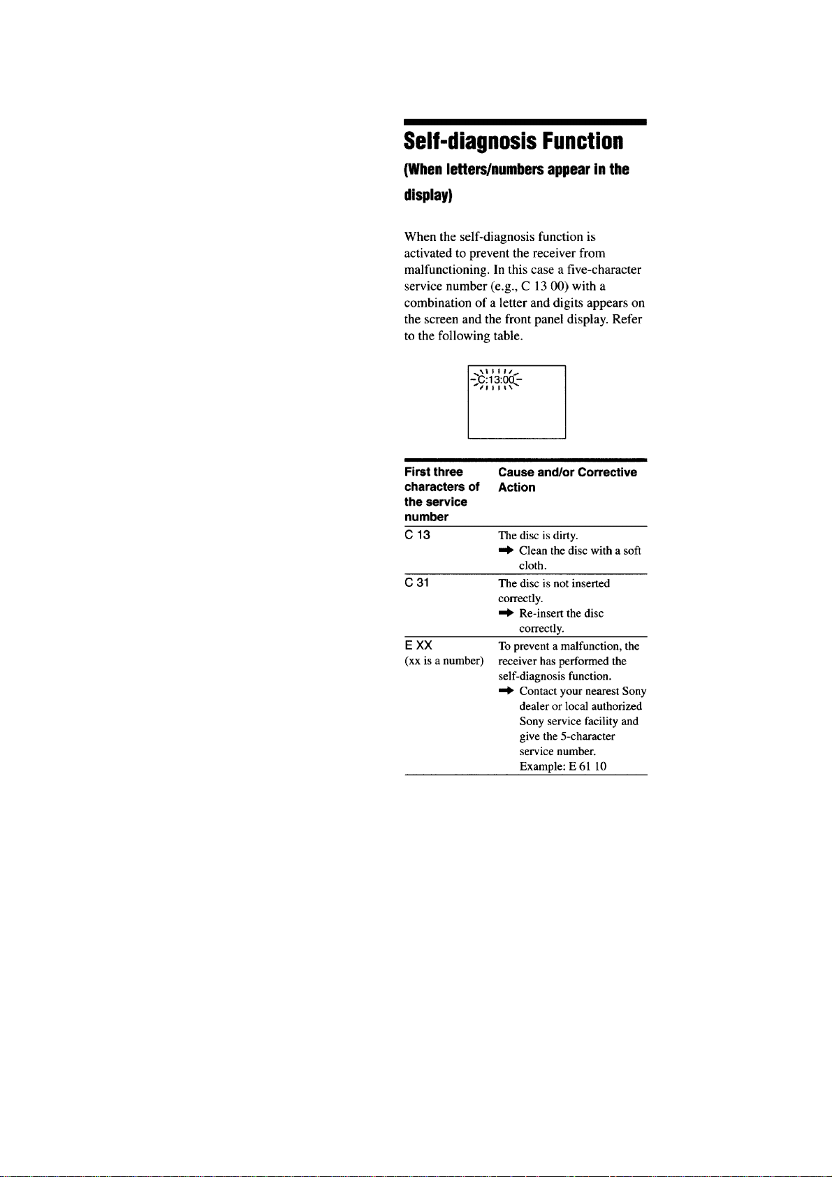
SELF DIAGNOSIS FUNCTION
General
Power requirements 120 V AC, 60 Hz
Power consumption 180 W
Dimensions (approx.) 430 × 135.5 × 455 mm (17 × 5
Mass (approx.) 9.8 kg (21 lb. 10 oz.)
Operating temperature 5 °C to 35 °C (41 °F to 95 °F)
Operating humidity 5 % to 90 %
Design and specifications are subject to change without notice.
1.5 W
(at the Power Saving Mode)
3/8 × 18 inches) (w/h/d)
incl. projecting parts
Note: Refer to the “4.TEST MODE” (page 16) for another self-
diagnosis function.
2
AVD-C70ES
1.5 k
Ω
0.15 µF
AC
voltmeter
(0.75 V)
To Exposed Metal
Parts on Set
Earth Ground
Ver 1.3
Notes on Chip Component Replacement
• Never reuse a disconnected chip component.
• Notice that the minus side of a tantalum capacitor may be dam-
aged by heat.
Flexible Circuit Board Repairing
• Keep the temperature of the soldering iron around 270˚C during
repairing.
• Do not touch the soldering iron on the same conductor of the
circuit board (within 3 times).
• Be careful not to apply force on the conductor when soldering
or unsoldering.
CAUTION
Use of controls or adjustments or performance of procedures
other than those specified herein may result in hazardous radiation exposure.
SAFETY CHECK-OUT
After correcting the original service problem, perform the following
safety check before releasing the set to the customer:
Check the antenna terminals, metal trim, “metallized” knobs, screws,
and all other exposed metal parts for A C leakage. Check leakage as
described below.
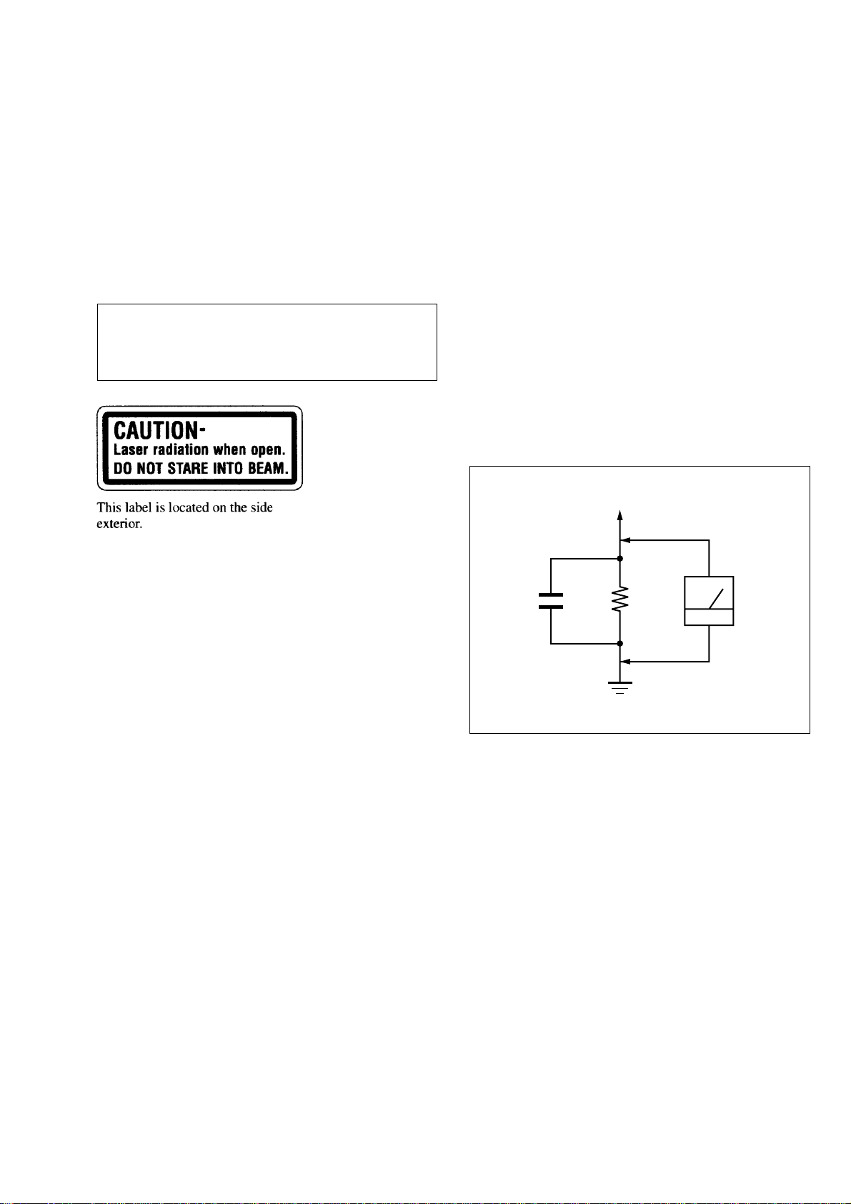
LEAKAGE TEST
The AC leakage from any exposed metal part to earth ground and
from all exposed metal parts to any exposed metal part having a
return to chassis, must not exceed 0.5 mA (500 microamperes).
Leakage current can be measured by any one of three methods.
1. A commercial leakage tester, such as the Simpson 229 or RCA
WT-540A. Follow the manufacturers’ instructions to use these
instruments.
2. A battery-operated AC milliammeter. The Data Precision 245
digital multimeter is suitable for this job.
3. Measuring the voltage drop across a resistor by means of a V OM
or battery-operated A C v oltmeter. The “limit” indication is 0.75
V, so analog meters must have an accurate low-voltage scale. The
Simpson 250 and Sanwa SH-63Trd are examples of a passive
VOM that is suitable. Nearly all battery operated digital
multimeters that have a 2V AC range are suitable. (See Fig. A)
LASER DIODE AND FOCUS SEARCH OPERATION
CHECK
Carry out the “S curve check” in “DVD section adjustment” and
check that the S curve waveforms is output three times.
NOTE OF REPLACING THE DVD BOARD
When replacing the DVD board, since the adjustment value is not
set up correctly, “Drive Auto Adjustment” can’t be performed.
In this case, initialize Memory in the following procedures.
Procedure:
1. Set the test mode. (See page 16)
2. Press the [2] key of the remote commander , and set the “DRIVE
MANUAL OPERATION”. (See page 18)
3. Press the [6] key of the remote commander, and set the “2-6,
Memory Check”. (See page 20)
4. Press the [CLEAR] key of the remote commander, and initialize
Memory.
Fig. A. Using an AC voltmeter to check AC leakage.
SAFETY-RELATED COMPONENT WARNING!!
COMPONENTS IDENTIFIED BY MARK 0 OR DOTTED LINE
WITH MARK 0 ON THE SCHEMATIC DIAGRAMS AND IN
THE PARTS LIST ARE CRITICAL TO SAFE OPERATION.
REPLACE THESE COMPONENTS WITH SONY P ARTS WHOSE
PART NUMBERS APPEAR AS SHOWN IN THIS MANUAL OR
IN SUPPLEMENTS PUBLISHED BY SONY.
ATTENTION AU COMPOSANT AYANT RAPPORT
À LA SÉCURITÉ!!
LES COMPOSANTS IDENTIFIÉS PAR UNE MARQUE 0 SUR LES
DIAGRAMMES SCHÉMATIQUES ET LA LISTE DES PIÈCES
SONT CRITIQUES POUR LA SÉCURITÉ DE FONCTIONNEMENT.
NE REMPLACER CES COMPOSANTS QUE PAR DES PIÈCES
SONY DONT LES NUMÉROS SONT DONNÉS DANS CE MANUEL
OU DANS LES SUPPLÉMENTS PUBLIÉS PAR SONY.
3

AVD-C70ES
TABLE OF CONTENTS
SELF DIAGNOSIS FUNCTION ........................................ 2
1. SERVICING NOTES ........................................................5
2. GENERAL
Location of Controls................................................................ 6
3. DISASSEMBLY ................................................................. 9
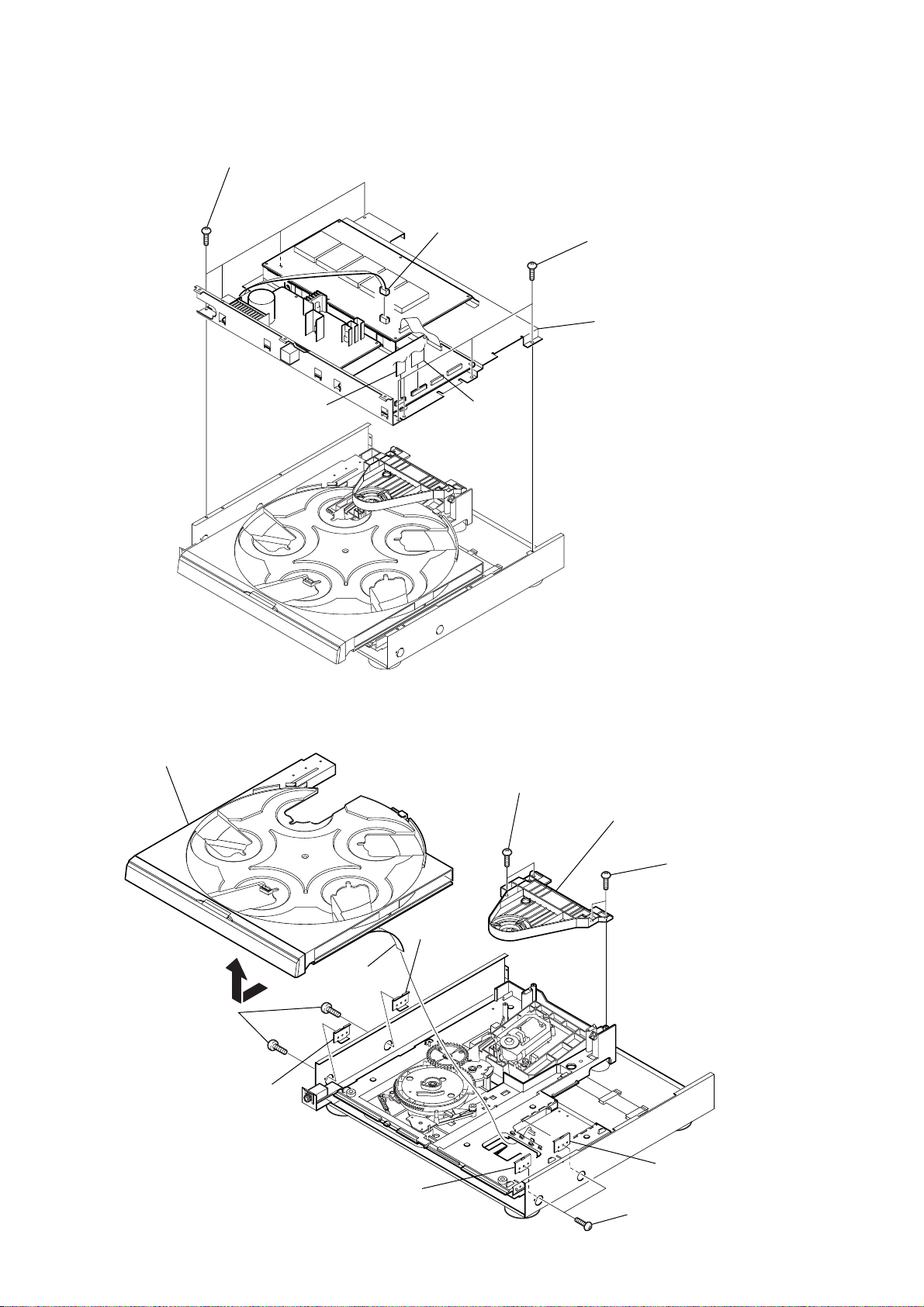
3-1. Case ................................................................................... 10
3-2. Front Panel Assy ............................................................... 10
3-3. Back Panel Assy ................................................................ 11
3-4. DVD Board, Power Board, Digital Amp Board................ 11
3-5. Boards Section .................................................................. 12
3-6. Table Assy ......................................................................... 12
3-7. Analog I/O Board, DVD Mechanism Block ..................... 13
3-8. Chassis Assy...................................................................... 13
3-9. Display Board ................................................................... 14
3-10. Sensor Board, Belt (RM), Motor Assy (Rotary) ............... 14
3-11. Belt (Timing), Motor Assy (B).......................................... 15
3-12. RF Board, Pick-up Unit .................................................... 15
4. TEST MODE .....................................................................16
5. DIAGRAMS
5-1. IC Pin Function Description ............................................. 23
5-2. Circuit Boards Location .................................................... 41
5-3. Note for Printed Wiring Boards and
Schematic Diagrams .......................................................... 42
5-4. Printed Wiring Board –RF Section– ................................. 44
5-5. Schematic Diagram –RF Section– ....................................45
5-6. Printed Wiring Board –DVD Section–.............................. 46
5-7. Schematic Diagram –DVD Section (1/10)–...................... 48
5-8. Schematic Diagram –DVD Section (2/10)–...................... 49
5-9. Schematic Diagram –DVD Section (3/10)–...................... 50
5-10. Schematic Diagram –DVD Section (4/10)–...................... 51
5-11. Schematic Diagram –DVD Section (5/10)–...................... 52
5-12. Schematic Diagram –DVD Section (6/10)–...................... 53
5-13. Schematic Diagram –DVD Section (7/10)–...................... 54
5-14. Schematic Diagram –DVD Section (8/10)–...................... 55
5-15. Schematic Diagram –DVD Section (9/10)–...................... 56
5-16. Schematic Diagram –DVD Section (10/10)–.................... 57
5-17. Printed Wiring Board –Digital Amp Section– .................. 58
5-18. Schematic Diagram –Digital Amp Section (1/2)– ............60
5-19. Schematic Diagram –Digital Amp Section (2/2)– ............61
5-20. Printed Wiring Board –Video Section–............................. 62
5-21. Schematic Diagram –Video Section–................................ 63
5-22. Printed Wiring Boards –In/Out Section– .......................... 64
5-23. Schematic Diagram –In/Out Section–............................... 65
5-24. Printed Wiring Boards –Display Section– ........................ 66
5-25. Schematic Diagram –Display Section–............................. 67
5-26. Printed Wiring Boards –Panel Section– ............................ 68
5-27. Schematic Diagram –Panel Section– ................................69
5-28. Printed Wiring Board –Speaker Section– ......................... 70
5-29. Schematic Diagram –Speaker Section– ............................71
5-30. Printed Wiring Boards –Power Section–........................... 72
5-31. Schematic Diagram –Power Section– ............................... 73
5-32. IC Block Diagrams............................................................ 74
6. EXPLODED VIEWS
6-1. Case Section ...................................................................... 84
6-2. Front Panel Section ...........................................................85
6-3. Back Panel Section............................................................ 86
6-4. Boards Section .................................................................. 87
6-5. Mechanism Section (1) ..................................................... 88
6-6. Mechanism Section (2) ..................................................... 89
6-7. Mechanism Section (3) ..................................................... 90
6-8. Base Unit Section .............................................................. 91
7. ELECTRICAL PARTS LIST ........................................92
4
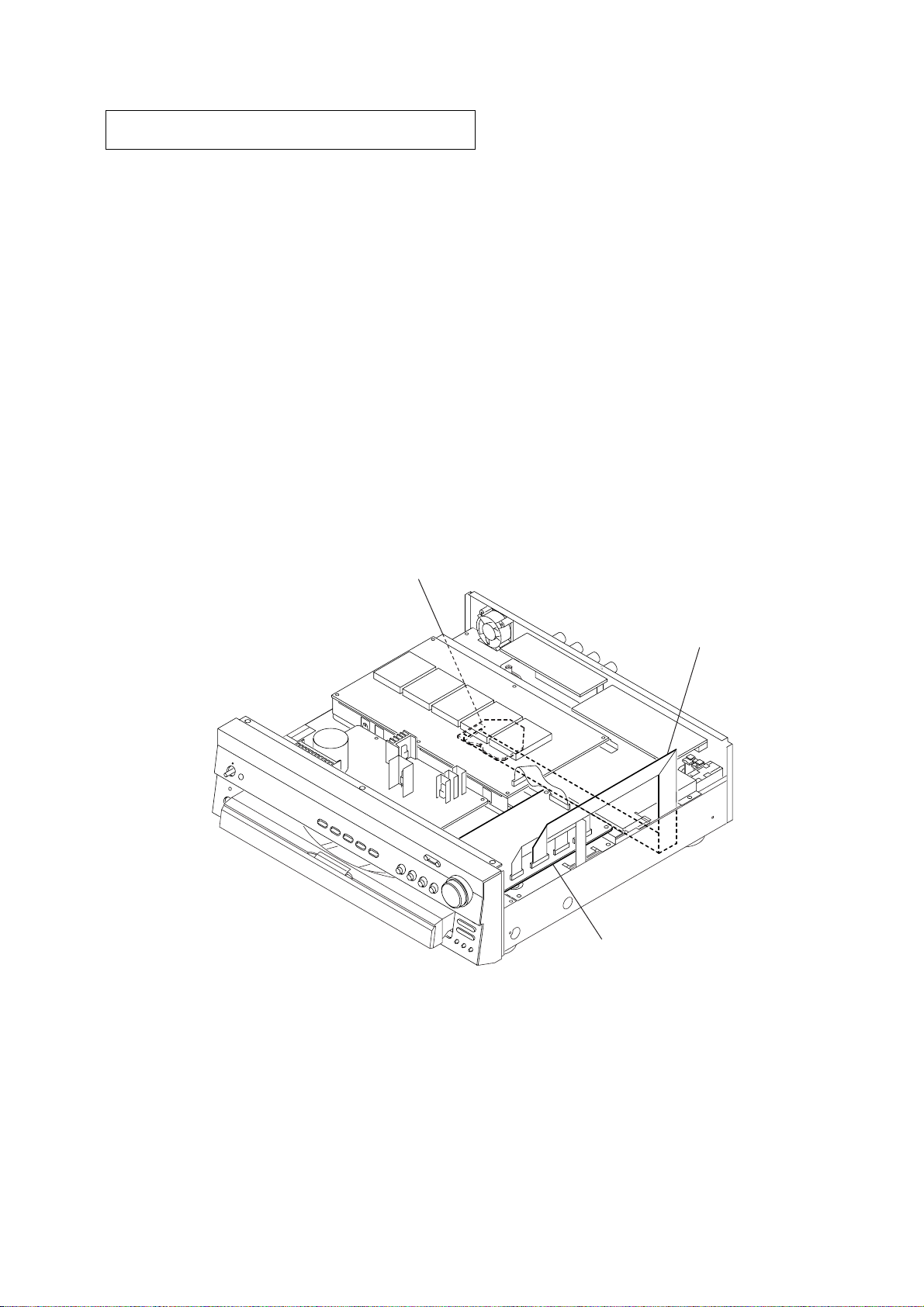
SECTION 1
SERVICING NOTES
AVD-C70ES
Ver 1.2
NOTES ON HANDLING THE OPTICAL PICK-UP
BLOCK OR BASE UNIT
The laser diode in the optical pick-up block may suffer electrostatic break-down because of the potential difference generated
by the charged electrostatic load, etc. on clothing and the human
body.
During repair, pay attention to electrostatic break-down and also
use the procedure in the printed matter which is included in the
repair parts.
The flexible board is easily damaged and should be handled with
care.
NOTES ON LASER DIODE EMISSION CHECK
The laser beam on this model is concentrated so as to be focused
on the disc reflective surface by the objective lens in the optical
pick-up block. Therefore, when checking the laser diode emission, observe from more than 30 cm away from the objecti ve lens.
JIG ON REPAIRING
When repairing this set, etc., connect the extension cable as the
figure shown below.
DISC TRAY LOCK
The disc tray lock function for the antitheft of an demonstration
disc in the store is equipped.
Releasing Procedure:
1. Press two buttons of [FUNCTION ] and [ PREV]
simultaneously.
2. The message “UNLOCKED” is displayed and the tray is
unlocked.
Note:When “LOCKED” is displayed, the tray lock is not released
by turning power on/off with the [POWER] button.
–
.
RF board
J-2501-217-A
DVD board
5
AVD-C70ES
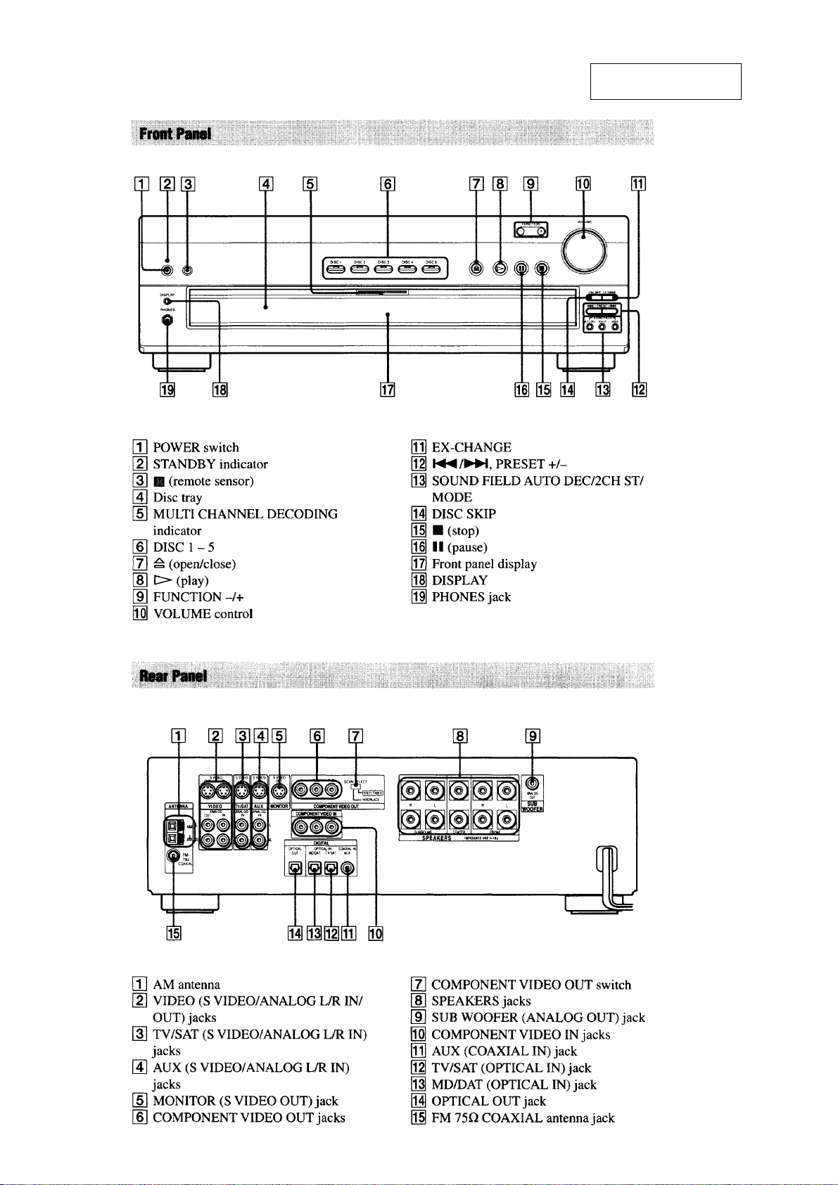
LOCATION OF CONTROLS
SECTION 2
GENERAL
This section is extracted
from instruction manual.
6
AVD-C70ES
7
AVD-C70ES
8

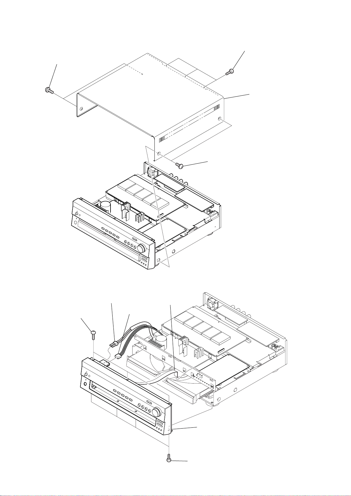
SECTION 3
DISASSEMBLY
Note: This set can be disassemble according to the following sequence.
SET
3-1. CASE
(Page 10)
AVD-C70ES
3-2. FRONT PANEL ASSY
(Page 10)
3-4. DVD BOARD,
POWER BOARD,
DIGITAL AMP
BOARD
(Page 11)
3-12. RF BOARD,
PICK-UP UNIT
(Page 15)
3-3. BACK PANEL ASSY
(Page 11)
3-5. BOARDS SECTION
(Page 12)
3-6. TABLE ASSY
(Page 12)
3-7. ANALOG I/O BOARD,
DVD MECHANISM BLOCK
(Page 13)
3-8. CHASSIS ASSY
(Page 13)
3-11. BELT (TIMING),
MOTOR ASSY (B)
(Page 15)
3-9. DISPLAY BOARD
(Page 14)
3-10. SENSOR BOARD,
BELT (RM),
MOTOR ASSY (ROTARY)
(Page 14)
9
AVD-C70ES
)
Note: Follow the disassembly procedure in the numerical order given.
3-1. CASE
2
two screws
(flat head screw)
1
two screws
(flat head screw)
3
three screws
(screw (BV/RING)
4
case
3-2. FRONT PANEL ASSY
4
three screws
(screw (BV/RING))
3
CNP905
2
CNP904
1
CN005
6
front panel assy
10
5
four screws
(BVTP 3x8)

3-3. BACK PANEL ASSY
)
8
CN305
7
CN306
6
CN307
5
CN308
3
CNP903
9
CN304
qa
screw
(screw (BV/RING))
qs
screw
(screw (BV/RING))
qd
three screws
(screw (BV/RING))
4
CN312
0
screw
(screw (BV/RING)
AVD-C70ES
1
CN003
3-4. DVD BOARD, POWER BOARD, DIGITAL AMP BOARD
qg
three screws
(BVTP 3x8)
6
two screws
(BVTP 3x8)
qs
0
three screws
(BVTP 3x8)
qa
POWER board
qh
two screws
(BVTP 3x8)
8
two screws
(BVTP 3x8)
CN300
9
CN301
qf
2
CN309
1
CN002
CN007
qf
back panel assy
qj
DIGITAL AMP board
3
CN001
4
CN008
5
7
two screws
(BVTP 3x10)
DVD board
qd
insulating sheet (PWB)
2
CN401
11
AVD-C70ES
n
)
3-5. BOARDS SECTION
4
four screws
(BVTP 3x8)
1
CN007
3
CN309
2
CN401
5
four screws
(BVTP 3x8)
6
boards sectio
3-6. TABLE ASSY
7
qs
table assy
two screws
(BVTP 3x8)
0
9
bracket
(guide B1)
qa
CN914
8
bracket
(guide B1)
2
two screws
(BVTP 3x8)
3
bracket (CP)
1
two screws
(BVTP 3x8
12
5
bracket
(guide B1)
6
4
two screws
(BVTP 3x8)
bracket
(guide B1)
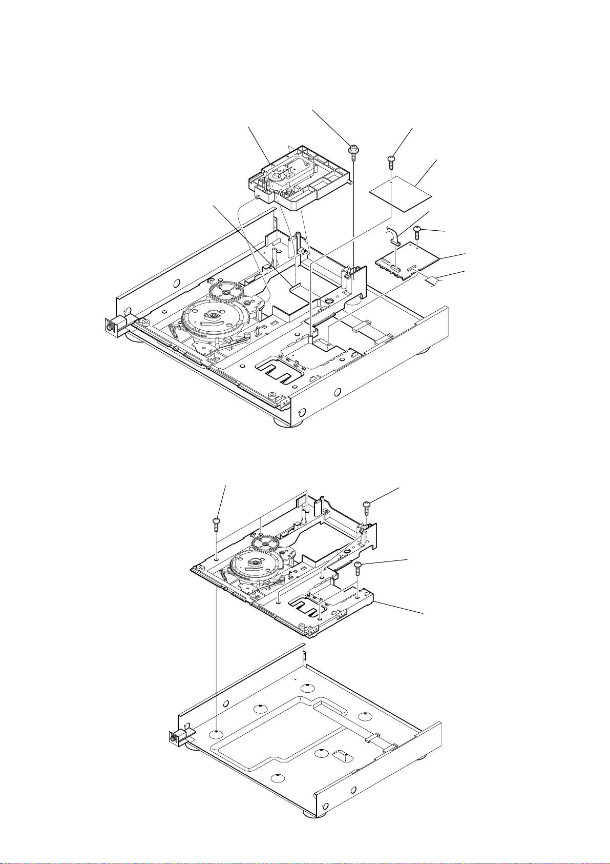
3-7. ANALOG I/O BOARD, DVD MECHANISM BLOCK
y
7
8
DVD mechanism block
9
CN002
screw (M 3x12)
2
screw (BVTP 3x8)
3
sheet (protection)
1
CN913
4
AVD-C70ES
screw (BVTP 3x8)
5
ANALOG I/O board
6
CN911
3-8. CHASSIS ASSY
3
three screws
(BVTP 3x8)
2
three screws
(BVTP 3x8)
1
two screws
(BVTP 3x8)
4
chassis ass
13

AVD-C70ES
d
3-9. DISPLAY BOARD
1
panel (loading) assy
claw
4
CN902
5
DISPLAY boar
3
cover FC
3-10. SENSOR BOARD, BELT (RM), MOTOR ASSY (ROTARY)
6
two screws
1
screw (M 3x12)
2
table (rotary)
8
two screws
(B 2.6x3)
7
bracket (rotary) assy
(BVTP 3x8)
2
three screws
(BVTP 3x10)
qs
T-125 board
qa
0
motor assy (rotary)
9
belt (RM)
Removal the solders.
14
5
SENSOR board
4
two screws
(BVTP 3x8)
3
CN962
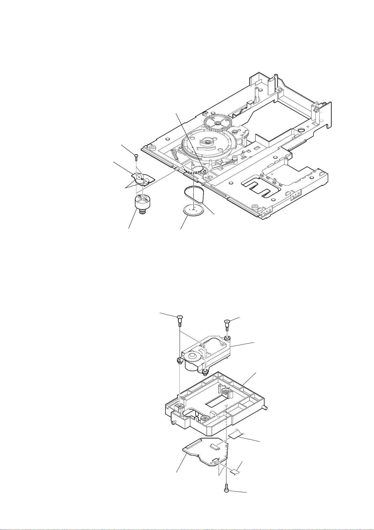
3-11. BELT (TIMING), MOTOR ASSY (B)
2
two screws
(BTTP M2.6)
3
RF board
1
CN003
4
CN001
6
screw
(step screw (M))
7
pick-up unit
holder (73) assy
5
two screws
(step screw (M))
3
two screws
(BVTP 3x8)
6
MOTOR board
5
Removal the solders.
AVD-C70ES
claw
4
3-12. RF BOARD, PICK-UP UNIT
motor assy (B)
1
pulley (flange B)
2
belt (timing)
15

AVD-C70ES
Ver 1.3
SECTION 4
TEST MODE
[GENERAL DESCRIPTION]
The T est Mode allows you to make dia gnosis and adjustment easily
using the remote commander and monitor TV. The instructions,
diagnostic results, etc. are given on the on-screen display (OSD).
[TEST DISC LIST]
Use the following test disc on test mode.
TDV-520CSO (DVD-SL) : PART No. J-2501-236-A
LUV-P01 (CD) : PART No. 4-999-032-01
TDV-540C (DVD-DL) : PART No. J-2501-235-A
Note: Do not use exiting test disc for DVD.
[STARTING TEST MODE]
1. Press the [POWER] button to turn the power on, and set the
function to DVD.
2. While pressing the x and [AUTO DEC] button, turn the
[VOLUME] knob clockwise to enter the test mode.
3. It displays “TEST MODE” on the fluorescent indicator tube,
and displays the Test Mode Menu on the monitor screen as
follows. (At the bottom of the menu screen, the model name
and revision number are displayed)
Test Mode Menu
0. Syscon Diagnosis
1. Drive Auto Adjustment
2. Drive Manual Operation
3. Mecha Aging
4. Emergency History
5. Version Information
6. Video Level Adjustment
Exit: POWER Key
Model :AVD-C70ES
Revision :x.xx
0-0. Quit
Quit the Syscon Diagnosis and return to the Test Mode Menu.
0-1. All (All items continuous check)
This menu checks all diagnostic items continuously. Normally, all
items are checked successively one after another automatically
unless an error is found, but at a certain item that requires judgment
through a visual check to the result, the following screen is displayed
for the key entry.
• Example display
### Syscon Diagnosis ###
Diag All Check
No.2 Version
2-3. ROM Check Sum
Check Sum = 2320
Press NEXT Key to Continue
Press PREV Key to Repeat
For the ROM Check, the check sum calculated by the Syscon is
output, and therefore you must compare it with the specified value
for confirmation.
Following the message, press the [NEXT ] button to go to the
next item, or press the [ PREV] button to repeat the same
operation again.
To quit the diagnosis and return to Check Menu screen, press the
.
>
[RETURN] key on the remote commander to display Check Menu.
4. To execute each function, select the desired menu and press its
number on the remote commander (RM-SS880J).
5. To release from test mode, press the
the power off.
[POWER] button and tur n
[OPERA TING TEST MODE]
0. SYSCON DIAGNOSIS
The same contents as board detail check by serial interface can be
checked from the remote commander operation.
On the Test Mode Menu screen, press [10/0] key on the remote
commander, and the following Check Menu will be displayed.
### Syscon Diagnosis ###
Check Menu
0. Quit
1. All
2. Version
3. EEPROM
4. SPIO
5. SD Bus
6. Video
7. Audio
• Error occurred
If an error occurred, the diagnosis is suspended and error is displayed.
Press the [RETURN] key on the remote commander to quit the
diagnosis, or press the [ PREV] button to repeat the same check
where an error occurred, or press the [NEXT ] button to continue
the check from the item next to faulty item.
General Description of Checking Method
Selecting 2 and subsequent items calls the submenu screen of each
item. And selecting 2 and subsequent items executes respective
menus and outputs the results.
For the contents of each submenu, see “Check Items List” as below .
Check Items List:
0-2. Version
0-2-1. All
0-2-2. Revision
0-2-3. ROM Check Sum
0-2-4. Model Type
0-2-5. Region
0-3. EEPROM Check
0-3-1. Sampling Check
0-3-2. Detail Check
0-4. GP I/O Check
0-5. SD Bus Check
0-6. Video Check
0-7. Audio Check
.
>
16

AVD-C70ES
Ver 1.3
0-2. Version
0-2-2. Revision
The revision number of ROM (IC204) that the program for
the DVD system processor (IC206) is stored.
(4 digits hexadecimal number)
0-2-3. ROM Check Sum
The revision number of ROM (IC204) that the program for
the DVD system processor (IC206) is stored.
0-2-4. Model Type
Model name is displayed.
0-2-5. Region
Model destination code is displayed. (2 digits number)
0-3. EEPROM Check
0-3-1. Sampling Check
EEPROM check at every 64 words.
It compares read data with write data of each address. When
there are discrepancies between two data, it displays error.
0-3-2. Detail Check
EEPROM check at every 1 word.
It compares read data with write data of each address. When
there are discrepancies between two data, it displays error.
0-4. GP I/O Check
Pull up/down setting check of the DVD system processor (IC206)
pin 150, 151 and 154 (for clock setting port).
0-5. SD Bus Check
SD bus data check between DVD decoder (IC701) and D-RAM
(IC706).
0-6. Video Check
Output the color bars for video level adjustment.
0-7. Audio Check
Output the test signal (1kHz sine wave) for 5.1 CH test.
1. DRIVE AUTO ADJUSTMENT
On the Test Mode Men u screen, press the [1] key on the remote
commander, and the Adjustment Menu will be displayed.
## Drive Auto Adjustment ##
Adjustment Menu
0. ALL
1. DVD-SL
2. CD
3. DVD-DL
1-0. ALL
Press the [10/0] key on the remote commander, and the servo set
data in EEPROM will be initialized. Then, 1. DVD-SL disc, 2. CD
disc and 3. DVD-DL disc are adjusted in this order.
Each time one disc was adjusted, it is ejected. Replace it with the
specified disc following the message. Y ou can finish the adjustment
by pressing the [RETURN] button on the remote commander.
Note: During adjustment of each disc, the measurement for disc type judg-
ment is made. As automatic adjustment does not judge the disc
type unlike conventional models, take care not to insert wrong type
discs. Also, do not give a shock during adjustment.
1-1. DVD-SL (single layer)
Press the [1] key on the remote commander and insert a DVD single
layer disc following the message. Then the adjustment will be made
through the steps below, then adjusted values will be written to the
EEPROM.
DVD Single Layer Disc Adjustment Steps:
1. Sled tilt reset
2. Disc check memory SL
3. Wait 300 msec
4. Set disc type SL
5. LD on
6. Spindle start
7. Wait 1 sec
8. Focus servo on 0
9. Auto track offset adjust
10. CLVA on
11. Wait 500 msec
12. Tracking on
13. Wait 1 sec
14. Sled on
15. Check CLV on
16. Auto LFO adjust
17. Auto focus offset adjust
18. Auto tilt position adjust
19. Auto focus gain adjust
20. Auto focus offset adjust
21. EQ boost adjust
22. Auto loop filter offset adjust
23. Auto track gain adjust
Search Check
24. 32 track jump forward
25. 32 track jump reverse
26. 500 track jump forward
27. 500 track jump reverse
28. All servo stop
29. EEP copy loop filter offset
1-2. CD
Press the
following the message. Then the adjustment will be made through
the steps below , then adjusted values will be written to the EEPR OM.
[2] key on the remote commander and insert a CD disc
Exit: RETURN
Normally, [10/0] is selected to adjust DVD (single layer), CD and
DVD (dual layer) in this order . But, individual items can be adjusted
for the case where adjustment is suspended due to an error. In this
mode, the adjustment can be made easily through the operation
following the message displayed on the screen.
The disc used for adjustment must be the one specified for
adjustment.
CD Adjustment Steps
1. Sled tilt rest
2. Disc check memory CD
3. Wait 500 msec
4. Set disc type CD
5. LD on
6. Spindle start
7. Wait 500 msec
8. Focus servo on 0
9. Auto track offset adjust
10. CLVA on
11. Wait 500 msec
17
AVD-C70ES
Ver 1.3
12. Tracking on
13. (TC display start)
14. Wait 1 sec
15. Jitter display start
16. Sled ON
17. Check CLV on
18. Auto loop filter offset adjust
19. Auto focus offset adjust
20. Auto focus gain adjust
21. Auto focus offset adjust
22. EQ boost adjust
23. Auto LFO Adjust
24. Auto track gain adjust
Search Check
25. 32Tj forward
26. 32Tj reverse
27. 500Tj forward
28. 500Tj reverse
29. All servo stop
1-3. DVD-DL (dual layer)
Press the [3] key on the remote commander and insert a DVD dual
layer disc following the message. Then the adjustment will be made
through the steps below, then adjusted values will be written to the
EEPROM.
DVD Dual Layer Disc Adjustment Steps:
1. Sled tilt reset
2. Disc check memory DL
3. Wait 500 msec
4. Set disc type DL
5. LD on
6. Spindle start
7. Wait 1 sec
Layer 1 Adjust
8. Focus servo on 0
9. Auto track offset adjust
10. CLVA on
11. Wait 500 msec
12. Tracking on
13. Wait 500 msec
14. Sled on
15. Check CLV lock
16. Auto loop filter offset adjust, Auto focus adjust
17. Auto focus gain adjust
18. Auto focus offset adjust
19. EQ boost adjust
20. Auto loop filter offset adjust
21. Auto Track Gain Adjust
Search Check
22. 32 track jump forward
23. 32 track jump reverse
24. 500 track jump forward
25. 500 track jump reverse
Layer 0 Adjust
26. Focus jump (L1 t L0)
27. Auto track offset adjust L0
28. CLVA on
29. Wait 500 msec
30. Tracking on
31. Wait 500 msec
32. Sled on
33. Check CLV lock
34. Auto focus filter offset adjust
35. Auto Focus Adjust
36. Auto focus gain adjust
37. Auto focus offset adjust
38. EQ boost adjust
39. Auto Loop Filter Offset
40. Auto track gain adjust
Search Check
41. 32 track jump forward
42. 32 track jump reverse
43. 500 track jump forward
44. 500 track jump reverse
Layer Jump Check
45. Layer jump (L0 ? L1)
46. Layer jump (L1 ? L0)
47. All servo stop
2. DRIVE MANUAL OPERATION
Note: This mode is used for design, and not used in service fundamen-
tally.
On the Test Mode Menu screen, press the [2] key on the remote
commander, and the Operation Menu will be displayed. For the
manual operation, each servo on/off control and adjustment can be
executed manually.
## Drive Manual Operation ##
Operation Menu
1. Disc Type
2. Servo Control
3. Track/Layer Jump
4. Non EEPROM Write Adjust
5. EEPROM Write Adjust
6. Memory Check
7. Disc Check Memory
8. Error Rate Display
9. SACD Water Mark
Exit: RETURN
In using the manual operation menu, take care of the following
points. These commands do not provide protection, thus requiring
correct operation. The sector address or time code field is displayed
when a disc is loaded.
Note:
1. Set correctly the disc type to be used on the Disc Type screen.
2. In case of an alarm, immediately press the x button to stop the
servo operation, and press the [POWER] button to turn the power
off.
Basic operation:
(controllable from front panel or remote commander)
[POWER] :Power OFF (release the Test Mode)
x : Servo stop
Z (DISC1 to 4) : Stop and eject/Loading
[RETURN] : Return to Operation Menu or Test
Mode Menu
[ PREV], [NEXT ] :Transition between sub modes of menu
.
>
[1] to [9], [10/0] : Selection of menu items
Cursor o/
O
: Increase/Decrease in manually
adjusted value
18

AVD-C70ES
2-1. Disc Type
Disc Type
Disc Type Select
1. Disc Type Auto Check
2. Set Disc Type DVD
3. Set Disc Type CD
4. Set Disc Type Hybrid
Exit: RETURN
2-1-1. Disc T ype Auto Check
1) Press the [1] key on the remote commander to display the Disc
Type Auto Check screen.
2) Insert a disc and press the [ENTER] key on the remote
commander.
3) It judges the type of inserted disc automatically and displays
the disc type and so on as below.
Disc Type Auto Check
Disc Type xx
Layer xx
Mirr Time xx
Mirr Count xx
FZC Count xx
PI Reference xx
PI Peak xx
2-1-3. Disc T ype CD
It sets up so that it may judge as a disc type of specification of the
disc with which the set was inserted.
[1]: CD disc (normal speed, 12 cm)
[2]: CD disc (double speed, 12 cm)
[3]: CD disc (normal speed, 8 cm)
[4]: CD disc (double speed, 8 cm)
[5]: CD-RW disc (normal speed, 12 cm)
[6]: CD-RW disc (double speed, 12 cm)
[7]: CD-RW disc (normal speed, 8 cm)
[8]: CD-RW disc (double speed, 8 cm)
2-1-4. Disc T ype Hybrid
It sets up so that it may judge as a disc type of specification of the
disc with which the set was inserted.
[1]: SACD Hybrid disc (SACD layer, 12 cm)
[2]: SACD Hybrid disc (CD layer, normal speed, 12 cm)
[3]: SACD Hybrid disc (CD layer, double speed, 12 cm)
[4]: SACD Hybrid disc (SACD layer, 8 cm)
[5]: SACD Hybrid disc (CD layer, normal speed, 8 cm)
[6]: SACD Hybrid disc (CD layer, double speed, 8 cm)
2-2. Servo Control
Note: Be sure to perform the disc type setup before performing this item.
Servo Control
1.LD off R.Sled FWD
2.Focus off L.Sled REV
3.SPDL off U.Sled Reset
4.CLVA off D.Sled Limit
5.Trk. off
6.Sled off
7.Fcs.Srch off
8.Fcs.OppL off
ENTER.Execute
Exit: RETURN
Disc Type : CD, DVD or Hybrid (SACD)
Layer : SINGLE, DUAL or HYBRID
Mirr Time : Mirror time of between disc surface and record
surface when disc type judgment. (hexadecimal
number)
Mirr Count : The number of times which mirror counts between
disc surface and record surface when disc type
judging. (hexadecimal number)
FZC Count : The number of times which focus zero cross points
of each layer when lens down. (hexadecimal number)
PI Reference : The average of PI reference voltage. (hexadecimal
number)
PI Peak : PI peak level voltage. It performs only when disc
type judgment is successful. (hexadecimal number)
2-1-2. Disc T ype D VD
It sets up so that it may judge as a disc type of specification of the
disc with which the set was inserted.
[1]: DVD single layer disc (12 cm)
[2]: DVD dual layer disc (0 layer, 12 cm)
[3]: DVD dual layer disc (1 layer, 12 cm)
[4]: DVD-RW disc (12 cm)
[5]: DVD single layer disc (8 cm)
[6]: DVD dual layer disc (0 layer, 8 cm)
[7]: DVD dual layer disc (1 layer, 8 cm)
0.All Servo Off
Exit: RETURN
On this screen, the servo on/off control necessary for replay is
executed. Normally, turn on each servo from 1 sequentially and
when CLVA is turned on, the usual trace mode becomes active. In
the trace mode, DVD sector address or CD time code is displayed.
This is not displayed where the spindle is not locked.
The spindle could run overriding the control if the spindle system is
faulty or RF is not present. In such a case, do not operate CLVA.
[1] LD : Turn on/off the laser.
[2] Focus : Search the focus and turn on the focus.
[3] SPDL :Turn on/off the spindle.
[4] CLVA : Turn on/off normal servo of spindle servo.
[5] Trk. : Turn on/off the tracking servo.
[6] Sled : Turn on/off the sled servo.
[7] FCS. Srch : Turn on/off the focus search.
[8] FCS. OppL : Turn on/off the focus search to another layer
of designated layer in Disc T ype setting. (dual
layer disc only)
[10/0] :All servo off.
[R] Sled FWD (right cursor) : Move the sled forward.
[L] Sled REV (left cursor) : Move the sled reverse.
[U] Sled FWD (up cursor) : Reset the sled.
[D] Sled REV (down cursor): Limit in the sled.
19
AVD-C70ES
2-3. Track/Layer Jump
Track/Layer Jump
1. 1Tj FWD R.Lj L0>L1
2. 1Tj REV L.Lj L1>L0
3.500Tj Fine FWD U.Fj L0>L1
4.500Tj Fine REV D.Fj L1>L0
5.10kTj Dirc FWD
6.10kTj Dirc REV
7.20kTj Dirc FWD
8.20kTj Dirc REV
0. All Servo Off
Exit: RETURN
On this screen, track jump, etc. can be performed. Only for the DVD
dual layer disc, the focus jump and layer jump are displayed in the
right field
[1] 1Tj FWD : 1 track jump forward.
[2] 1Tj REV : 1 track jump reverse.
[3] 500Tj FWD: 500 track jump (fine search)forward.
[4] 500Tj REV : 500 track jump (fine search) reverse.
[5] 10kTj FWD: 10k track jump (direct search) forward.
[6] 10kTj REV : 10k track jump (direct search) reverse.
[7] 20kTj FWD: 20k track jump (direct search) forward.
[8] 20kTj REV : 20k track jump (direct search) reverse.
[10/0] : All servo off.
2-4. Non EEPROM Write Adjust
2-5. EEPROM Write Adjust
EEPROM Write Adjust
1. Focus Offset
2. Focus Gain
3. Trk. Offset Coarse
4. ——————
5. Trk. Gain
6. EQ Boost
0.All Servo Off
Exit: RETURN
On this screen, each item can be adjusted automatically. Select the
desired number
selected item is adjusted automatically.
[1] to [10/0] from the remote commander, and
[1] Focus Offset: Adjusts focus offset.
[2] Focus Gain : Adjusts focus gain.
[3] TRK. Offset : Adjusts tracking offset of the RF amp
(IC001) side.
[5] TRK. Gain : Adjusts track gain.
[6] EQ Boost : Adjusts amount of boost of equalizer.
[10/0] : All servo off.
2-6. Memory Check
Display images are shown as follows, and all two screens are able
to switch by theOkey (UP) or okey (DW).
Non EEPROM Write Adjust
1. Focus Offset
2. Focus Gain
3. Trk. Offset Coarse
4. Trk. Offset Fine
5. Trk. Gain
6. EQ Boost
0.All Servo Off
Exit: RETURN
On this screen, each item can be adjusted manually. Select the desired
number
setting for the selected item will be displayed, then increase or
decrease numeric value with theOkey or okey. This value is
stored in the EEPROM. If CLV has been applied, the jitter is
displayed for reference for the adjustment.
[1] to [10/0] from the remote commander, and current
[1] Focus Offset: Adjusts focus offset.
[2] Focus Gain : Adjusts focus gain.
[3] TRK. Offset : Adjusts tracking offset of the RF amp
(IC001) side.
[4] TRK. Offset : Adjusts tracking offset of the DSP (IC401)
side.
[5] TRK. Gain : Adjusts track gain.
[6] EQ Boost : Adjusts amount of boost of equalizer.
[10/0] : All servo off.
EEPROM Data 1/2 CD SL L0 L1
Focus Gain xx xx xx xx
Trk. Gain xx xx xx xx
Focus Offset xx xx xx xx
Trk. Offset xx xx xx xx
EQ. Boost xx xx xx xx
PI Level xx xx -- -Fcs. Balance -- xx -- -Jitter xx xx xx xx
Mirror Time xx xx xx -FE Level -- xx -- -Traverse Lv1. -- xx -- -Next:DW Default:CLR Exit:RET
EEPROM Data 2/2 CDRW DVDRW
Focus Gain xx xx
Trk. Gain xx xx
Focus Offset xx xx
Trk. Offset xx xx
EQ. Boost xx xx
Next:UP Default:CLR Exit:RET
On this screen, current servo adjusted data stored in the EEPROM
are displayed. The adjusted data are initialized by pressing the
[CLEAR] key, but be careful that they are not recoverable after
initialization.
Before clearing the adjusted data, make a note of the set data. This
screen will also appear if [0]-All is selected in the Drive Auto
Adjustment. In this case, default setting cannot be made.
20

AVD-C70ES
2-7. Disc Check Memory
Disc Check Memory
1. SL Disc check
2. CD Disc check
3. DL Disc check
Exit: RETURN
On this screen, measure the mirror time of chucked disc, and write
to the EEPROM.
2-8. Error Rate Display
Error Rate Display
UC CR ADD
PI1 Err Now xx xxxx xxxxxxxx
Max xx xxxx xxxxxxxx
Avg xx xxxx xxxxxxxx
PI2 Err Now xx xxxx xxxxxxxx
Max xx xxxx xxxxxxxx
Avg xx xxxx xxxxxxxx
PO Err Now xx xxxx xxxxxxxx
Max xx xxxx xxxxxxxx
Avg xx xxxx xxxxxxxx
Exit: RETURN
On this screen, measure and display the error rate.
3. MECHA AGING
On the T est Mode Menu screen, selecting [3] executes the aging of
the mechanism deck.
### Aging Test MENU ###
Operation Menu
1. Open/Close Test
Exit: RETURN
1) On the Aging Test MENU screen, press the [1] key on the
remote commander to display the Open/Close Test screen.
2) Insert discs and press the [ENTER] key on the remote
commander.
3) Is starts the aging.
During aging, the disc number, operating status and repeat cyc le
are displayed. Aging can be aborted at any time by pressing
the x key. After the operation is stopped, press the x key or
[RETURN] key aging to return to the Aging Test MENU.
4. EMERGENCY HISTORY
On the Test Mode Menu screen, selecting [4] displays the
information such as servo emergency history.
The history information from last 1 up to 10 can be scrolled with
theOkey orokey. Also, specific information can be displayed
by directly entering that number with ten keys.
UC : Incorrect value
CR : Correct value
Add: Address
2-9. SACD Water Mark Check
SACD Water Mark Check
PSP AMP
PSN
Start: ENTER Exit: RETURN
On this screen, measure the PSP AMP v alue and PSN value of SACD
water mark.
### EMG. History ###
Laser Hours CD xxxxhxxm
DVD xxxxhxxm
a. bb xx xx xx xx xx xx xx
xx xx xx xx xx xx xx xx
a. bb xx xx xx xx xx xx xx
xx xx xx xx xx xx xx xx
Select:1-9 Scroll:UP/DOWN
(1.Latest EMG.) Exit: RETURN
xxxxhxxm: The laser on total hours. Data below minutes are
omitted.
a. : Error number.
bb : Error code.
xx : Not used.
• Clearing History Information
Clearing laser hours:
Press the
Then both CD and DVD data are cleared.
Clearing emergency history:
Press the [DVD TOP MENU] and [CLEAR] keys in this order.
Initializing set up data:
Press [DVD MENU] and [CLEAR] keys in this order.
The data have been initialized when “Set Up Initialized”
message is displayed. The EMG. History screen will be restored
soon.
[DVD DISPLAY] and [CLEAR] keys in this order.
21
AVD-C70ES
Ver 1.2
• Code list of Emergency History
10: Communication to RF AMP (IC001) failed.
11: Each servo for focus, tracking, and spindle is unlocked.
12: Check sum error of EEPROM (IC203).
14: Communication to servo DSP (IC401) failed , or serv o DSP
decoder (IC801) is faulty.
15: Communication to DVD decoder (IC701) failed, or DVD
decoder (IC801) is faulty.
16: Communication to DSD decoder (IC801) failed, or DSD
decoder (IC801) is faulty.
20: Initialization of sled servo failed. It is not placed in the ini-
tial position.
23: Sled servo operation error.
24: Made a request to move the sled servo to wrong position.
30: Tracking balance adjustment error.
31: Tracking gain adjustment error.
33: Focus bias adjustment error.
34: Focus gain adjustment error.
35: Equalizer adjustment error.
40: Focus servo does not operate.
41: With a DVD dual layer disc, focus jump failed.
50: CLV (spindle) servo does not operate.
51: Spindle does not stop.
60: Made a request to seek nonexistent address.
61: Seek error of retry more than regulated times.
70: Control data could not be read.
80: Disc reading failed.
5. MECHA ERROR HISTORY
On the T est Mode Menu screen, selecting [5] displays the information
of mechanism deck error history.
The history information from last 1 up to 8 can be scrolled with the
key orokey. Also, specific information can be displayed by
O
directly entering that number with ten keys.
### Mecha Error History ###
1. aa bb cc dd xx xx xx xx
2. aa bb cc dd xx xx xx xx
3. aa bb cc dd xx xx xx xx
4. aa bb cc dd xx xx xx xx
5. aa bb cc dd xx xx xx xx
6. aa bb cc dd xx xx xx xx
7. aa bb cc dd xx xx xx xx
8. aa bb cc dd xx xx xx xx
Scroll:UP/DOWN
(1.Latest Err.) Exit: RETURN
50 : Disc eject failing in the midst of initializing the mechanism
deck.
5x : Initializing the mechanism deck.
A2 : Disc eject failing in the midst of initializing the mechanism
deck.
Ax : Initializing the mechanism deck.
D3 : Disc eject failing in the midst of initializing the mechanism
deck.
Dx : Initializing the mechanism deck.
Ex : Initializing the mechanism deck.
• Error code (bb)
00 : Initializing the mechanism deck.
10 : Retry over of eject and loading.
30 : Open operation in no disc status.
60 : Retry over of eject and loading.
70 : Disc is chucking position.
81 : Retry failed of disc movement from chucking position to
stocker.
83 : Retry preparation failed of disc movement from chucking
position to stocker.
90 : Disc is stored in the stocker.
A1 : Retry failed of disc movement from stocker to chucking
position.
A3 : Retry preparation failed of disc movement from stocker to
chucking position.
B0 : Just before the release operation.
B1 : Retry failed of the release operation.
• Error code (cc)
10 : Under a stop.
22 : Retry preparation failed.
23 : Retry failed.
• Error code (dd)
10 : Under a stop.
22 : Retry preparation failed.
23 : Retry failed.
6. VERSION INFORMATION
On the Test Mode Menu screen, selecting [6] displays the ROM
version and region code.
The parenthesized hexadecimal number in version field is checksum
value of ROM.
## Version Information ##
IF con. Ver.x. xx
aa : The error in the midst of initializing the mechanism deck.
bb : The error in the midst of loading operation.
cc : The error in the midst of up/down the stocker.
dd : The error in the midst of switching the mechanism deck mode.
xx : Not used.
• Error code (aa)
FF : Complete the initializing. (normal operation)
11 : Stocker movement (to chucking position) failing in the midst
of initializing the mechanism deck.
12 : Stocker movement (to chucking position) failing in the midst
of initializing the mechanism deck.
1x : Initializing the mechanism deck.
2x : Initializing the mechanism deck.
3x : Initializing the mechanism deck.
41 : Disc eject failing in the midst of initializing the mechanism
deck.
4x : Initializing the mechanism deck.
22
SYScon. Ver.x. xx (xxxx)
Model AVD-C70ES
Region 0x
Front End Ver.x.xx
Exit: RETURN
IF con. : The version of system controller (IC901).
SYScon. : The version of DVD system processor (IC206).
Front End: The version of mechanism controller (IC301).
7. VIDEO LEVEL ADJUSTMENT
On the Test Mode Menu screen, selecting [7] displa ys color bars
for video level adjustment. During display of color bars, OSD
disappears but the menu screen will be restored if pressing the
[RETURN] key.
AVD-C70ES
SECTION 5
DIAGRAMS
5-1. IC PIN FUNCTION DESCRIPTION
• DVD BOARD IC301 CXP973064-233R (MECHANISM CONTROLLER)
Pin No. Pin Name I/O Pin Description
1 EEP SO O Not used. (Open)
2SDEN O Serial data enable signal output to DVD/CD RF amplifier
3
4 EEP WC O Not used. (Open)
5 EEP SI I/O Two-way data bus with the EEPROM
6 EEP RDY I EEPROM ready signal input from the DVD decoder
7 FCS JMP 1 O Focus jump 1 signal output to the motor/coil driver
8 FCS JMP 2 O Focus jump 2 signal output to the motor/coil driver
9 SENS CD I Internal status (SENSE) signal input from the digital signal processor
10 LOAD + O Loading motor drive signal (loading in direction) output terminal Not used. (Open)
11 LOAD – O Loading motor drive signal (loading out direction) output terminal Not used. (Open)
12 XCS DVD O Chip select signal output to the DVD decoder
13 VSS — Ground terminal (digital system)
14 to 21 D0 to D7 I/O Two-way data bus with the DVD decoder
22 INIT0 DVD I Interrupt signal input from the DVD decoder
23 INIT1 DVD I Interrupt signal input from the DVD decoder
24 FCOMP H O Serial data transfer clock signal output to the DSD decoder
25 FCOMP L O Reset signal output to the DVD decoder “L”: reset
26 SCOR I Subcode sync (S0+S1) detection signal input from the digital signal processor
27 LAT CD O Serial data latch pulse signal output to the digital signal processor
28 LD ON O
29 MIRR I Mirror signal input from the digital signal processor
30 COUT CD I Numbers of track counted signal input from the digital signal processor
31 INLIM I
32 CS ZIVA O Chip select signal output to the DVD system processor
33 SI ZIVA I Serial data input from the DVD system processor
34 SO ZIVA O Serial data output to the DVD system processor
35 SCK ZIVA O Serial data transfer clock signal output to the DVD system processor
36 DRVIRQ O Interrupt request signal output to the DVD system processor
37 DRVRDY O Ready signal output to the DVD system processor
38 RST I System reset signal input from the DVD system processor “L”: reset
39 VSS — Ground terminal (digital system)
40 XTAL I System clock input terminal (20 MHz)
41 EXTAL O System clock output terminal (20 MHz)
42 VDD — Power supply terminal (+3.3 V) (digital system)
43, 44 SLED A, SLED B O Sled motor drive signal output
45 SCK DSD O Output terminal for offset adjustment of APEO
46 SDOUT DSD O Serial data output to the DSD decoder
47 SDIN DSD I Serial data input from the DSD decoder
48 READY DSD I Ready signal input from the DSD decoder “L”: ready
49 DATA CD O Serial data output to the digital signal processor
50 CLOK CD O Serial data transfer clock signal output to the digital signal processor
51 XMSLAT O Serial data latch pulse signal output to the DSD decoder
52 SQSO I Subcode Q data input from the digital signal processor
DOCTRL/
ISBTEST “L”: digital out off, “H”: digital out on
Digital out on/off contrrol signal output to the digital signal processor
O
Laser diode on/off control signal output to the DVD/CD RF amplifier
“L”: laser diode off, “H”: laser diode on
Detection signal input from limit in switch
The optical pick-up is inner position when “H”
23

AVD-C70ES
Pin No. Pin Name I/O Pin Description
53 MUTE DSD O Muting on/off control signal output to the DSD decoder “H”: muting on
54 SQCK O Subcode Q data reading clock signal output to the digital signal processor
55 VSS — Ground terminal (digital system)
56 TRAY IN I Disc tray in detection signal input terminal Not used. (Fixed at “L” in this set.)
57 TRAY OUT I Disc tray out detection signal input terminal Not used. (Fixed at “L” in this set.)
58 GFS DVD I Guard frame sync signal input from the DVD decoder
59 MUTE CD O Muting on/off control signal output to the digital signal processor “H”: muting on
60 MUTE 2D O Muting on/off control signal output to the motor/coil driver “H”: muting on
61 SLED I Sled motor servo drive PWM signal input terminal
62 FG I Spindle motor control signal input
63 SP ON O Muting on/off control signal output to the motor/coil driver “H”: muting on
64 JIT I Jitter signal input
65 TE I Tracking error signal input from the DVD/CD RF amplifier
66 PI I Pull in signal input from the DVD/CD RF amplifier
67 FE I Focus error signal input from the DVD/CD RF amplifier
68 AVSS — Ground terminal (for A/D converter)
69 AVREF I Reference voltage input terminal (for A/D converter)
70 AVDD — Power supply terminal (+3.3 V) (for A/D converter)
71 GFS CD I Guard frame sync signal input from the digital signal processor
72 SCLK CD O SENSE serial data reading clock signal output to the digital signal processor
73 TSD M O Thermal shut down signal output to the motor/coil driver
74 FOK CD I Focus OK signal input from the digital signal processor
75 LOCK CD I GFS is sampled by 460 Hz “H” input when GFS is “H”
76 LDSEL O Laser diode selection signal output
77 SACD/DVD O SACD/DVD selection signal output “L”: DVD, “H”: SACD
78 I2C SIO I/O Communication data bus with the DVD system processor and system controller
79 I2C SCL I/O
80 RXD I Serial data input from the RS-232C (for check)
81 TXD O Serial data output to the RS-232C (for check)
82 SDCLK RF O Serial data transfer clock signal output to the DVD/CD RF amplifier
83 SDATA RF I/O Two-way data bus with the DVD/CD RF amplifier
84 XWR O Write strobe signal output to the DVD decoder
85 XRD O Read strobe signal output to the DVD decoder
86 (PWE) — Not used.
87 VDD — Power supply terminal (+3.3 V) (digital system)
88 VSS — Ground terminal (digital system)
89 to 96 A0 to A7 O Address signal output to the DVD decoder
97 A8 O Motor/coil driver power save control signal output terminal
98 XDRST O Reset signal output to the digital signal processor and DSD decoder “L”: reset
99 EEP WP O Write protect signal output to the EEPROM
100 EEP CLK O Clock signal output to the EEPROM
Communication data reading clock signal input or transfer clock signal output with
the DVD system processor and system controller
24
AVD-C70ES
• DVD BOARD IC401 CXD3068Q (DIGITAL SIGNAL PROCESSOR, DIGITAL SERVO PROCESSOR)
Pin No. Pin Name I/O Pin Description
1DVDD0 — Power supply terminal (+3.3 V) (digital system)
2 XRST I Reset signal input from the mechanism controller “L”: reset
3 MUTE I Muting on/off control signal input from the mechanism controller “H”: muting on
4DATAISerial data input from the mechanism controller
5 XLAT I Serial data latch pulse signal input from the mechanism controller
6 CLOK I Serial data transfer clock signal input from the mechanism controller
7 SENS O Internal status (SENSE) signal output to the mechanism controller
8 SCLK I SENSE serial data reading clock signal input from the mechanism controller
9ATSK I/O Input/output terminal for anti-shock Not used.
10 WFCK O Write frame clock signal output to the DVD decoder
11 RFCK O RFCK signal output terminal Not used.
12 XPCK O XPCK signal output terminal Not used.
13 GFS O Guard frame sync signal output to the mechanism controller
14 C2PO O C2 pointer signal output to the DVD decoder
15 SCOR O
16 C4M O 4.2336 MHz clock signal output terminal Not used.
17 WDCK O Guard subcode sync (S0+S1) detection signal output to the DVD decoder
18 DVSS0 — Ground terminal (digital system)
19 COUT O Numbers of track counted signal output to the mechanism controller
20 MIRR O Mirror signal output to the mechanism controller
21 DFCT I/O Defect signal input/output terminal Not used.
22 FOK O Focus OK signal output to the mechanism controller
23 PWMI I Spindle motor external control signal input terminal Not used.
24 LOCK O GFS is sampled by 460 Hz “H” output when GFS is “H”.
25 MDP O Spindle motor servo drive signal output to the DVD decoder
26 SSTP I
27 FSTO O 2/3 divider output terminal Not used.
28 DVDD1 — Power supply terminal (+3.3 V) (digital system)
29 SFDR O Sled servo drive PWM signal (+) output
30 SRDR O Sled servo drive PWM signal (–) output
31 TFDR O Tracking servo drive PWM signal (+) output
32 TRDR O Tracking servo drive PWM signal (–) output
33 FFDR O Focus servo drive PWM signal (+) output
34 FRDR O Focus servo drive PWM signal (–) output
35 DVSS1 — Ground terminal (digital system)
36 TEST I Input terminal for the test
37 TES1 I Input terminal for the test
38 VC I Middle point voltage (+1.65 V) input terminal
39 FE I Focus error signal input from the DVD/CD RF amplifier
40 SE I Sled error signal input from the DVD/CD RF amplifier
41 TE I Tracking error signal input from the DVD/CD RF amplifier
42 CE I Middle point servo analog signal input
43 RFDC I RF signal input from the DVD/CD RF amplifier
44 ADIO O Output terminal for the test Not used.
45 AVSS0 — Ground terminal (analog system)
46 IGEN I Stabilized current input for operational amplifiers
Subcode sync (S0+S1) detection signal output to the DVD decoder and mechanism
controller
Detection signal input from limit in switch
The optical pick-up is inner position when “H”
25

AVD-C70ES
Pin No. Pin Name I/O Pin Description
47 AVDD0 — Power supply terminal (+3.3 V) (analog system)
48 ASYO O EFM full-swing output terminal
49 ASYI I Asymmetry comparator voltage input terminal
50 RFAC I EFM signal input from the DVD/CD RF amplifier
51 AVSS1 — Ground terminal (analog system)
52 CLTV I Internal VCO control voltage input terminal
53 FILO O Filter output for master PLL
54 FILI I Filter input for master PLL
55 PCO O Charge pump output for master PLL
56 AVDD1 — Power supply terminal (+3.3 V) (analog system)
57 BIAS I Asymmetry circuit constant current input terminal
58 VCTL I VCO control voltage input terminal for the wideband EFM PLL Not used.
59 V16M O VCO oscillation output terminal for the wideband EFM PLL Not used.
60 VPCO O Charge pump output terminal for the wideband EFM PLL Not used.
61 DVDD2 — Power supply terminal (+3.3 V) (digital system)
62 ASYE I Asymmetry circuit on/off control signal input terminal “L”: off, “H”: on Not used.
63 MD2 I
64 DOUT O Digital audio signal output to the digital audio interface IC
65 LRCK O L/R sampling clock signal (44.1 kHz) output to the DVD decoder
66 PCMD O Serial data output to the DVD decoder
67 BCK O Bit clock signal (2.8224 MHz) output to the DVD decoder
68 EMPH O
69 XTSL I
70 DVSS2 — Ground terminal (digital system)
71 XTAI I System clock input terminal (33.8688 MHz)
72 XTAO O System clock output terminal (33.8688 MHz) Not used.
73 SOUT O Serial data output terminal Not used.
74 SOCK O Serial data reading clock signal output terminal Not used.
75 XOLT O Serial data latch pulse signal output terminal Not used.
76 SQSO O Subcode Q data output to the mechanism controller
77 SQCK I Subcode Q data reading clock signal input from the mechanism controller
78 SCSY I Input terminal for resynchronism of guard subcode sync (S0+S1) Not used.
79 SBSO O Subcode serial data output to the DVD decoder
80 EXCK I Subcode serial data reading clock signal input to the DVD decoder
Digital out on/off control signal input from the mechanism controller
“L”: digital out off, “H”: digital out on
“L” is output when playback disc is emphasis off
“H” is output when playback disc is emphasis on Not used.
Input terminal for the system clock frequency setting
“L”: 16.9344 MHz, “H”: 33.8688 MHz Fixed at “H” in this set.
26
AVD-C70ES
• DVD BOARD IC607 CXD9617R (AUDIO DIGITAL SIGNAL PROCESSOR)
Pin No. Pin Name I/O Pin Description
1 VSS — Ground terminal
2 XRST I Reset signal input from the system controller “L”: reset
3 EXTIN I Master clock signal input terminal Not used. (Fixed at “L” in this set.)
4 FS2 I Sampling frequency selection signal input terminal Not used. (Fixed at “L” in this set.)
5 VDDI — Power supply terminal (+2.6 V)
6 FS1 I Sampling frequency selection signal input terminal Not used. (Fixed at “L” in this set.)
7 PLOCK O Internal PLL lock signal output terminal Not used. (Open)
8 VSS — Ground terminal
9 MCLK1 I System clock signal input terminal (13.5 MHz)
10 VDDI — Power supply terminal (+2.6 V)
11 VSS — Ground terminal
12 MCLK2 O System clock signal output terminal (13.5 MHz)
13 MS I
14 SCKOUT O Internal system clock signal output to the D/A converter and stream processor
15 LRCKI1 I L/R sampling clock signal (44.1 kHz) input from the digital audio processor
16 VDDE — Power supply terminal (+3.3 V)
17 BCKI1 I Bit clock signal (2.8224 MHz) input from the digital audio processor
18 SDI1 I Front L-ch and R-ch audio serial data input from the digital audio processor
19 LRCKO O L/R sampling clock signal (44.1 kHz) output to the D/A conv erter and stream processor
20 BCKO O Bit clock signal (2.8224 MHz) output to the D/A converter and stream processor
21 VSS — Ground terminal
22 KFSIO I Audio clock signal (11.2896 MHz) input from the digital audio processor
23 SDO1 O Front L-ch and R-ch audio serial data output to the stream processor
24 SDO2 O Center and woofer audio serial data output to the stream processor
25 SDO3 O Rear L-ch and R-ch audio serial data output to the stream processor
26 SDO4 O Audio serial data output to the D/A converter
27 SPDIF O S/PDIF signal output terminal Not used. (Open)
28 LRCKI2 I L/R sampling clock signal (44.1 kHz) input from the A/D converter
29 BCKI2 I Bit clock signal (2.8224 MHz) input from the A/D converter
30 SDI2 I Center and woofer audio serial data input from the digital audio processor
31 VSS — Ground terminal
32 HACN O Acknowledge signal output to the system controller
33 HDIN I Write data input from the system controller
34 HCLK I Clock signal input from the system controller
35 HDOUT O Read data output to the system controller
36 HCS I Chip select signal input from the system controller
37 SDCLK O Clock signal output terminal Not used. (Open)
38 CLKEN O Clock enable signal output terminal Not used. (Open)
39 RAS O Row address strobe signal output terminal Not used. (Open)
40 VDDI — Power supply terminal (+2.6 V)
41 VSS — Ground terminal
42 CAS O Column address strobe signal output terminal Not used. (Open)
43 DQM O Output terminal of data input/output mask Not used. (Open)
44 CS0 O Chip select signal output to the S-RAM
45 WE0 O Write enable signal output to the S-RAM
Master/slave selection signal input terminal
“L”: slave, “H”: master (fixed at “L” in this set.)
27

AVD-C70ES
Pin No. Pin Name I/O Pin Description
46 VDDE — Power supply terminal (+3.3 V)
47 WMD1 I S-RAM wait mode setting terminal Fixed at “H” in this set
48 VSS — Ground terminal
49 WMD0 I S-RAM wait mode setting terminal Fixed at “L” in this set
50 PAGE2 O Page selection signal output terminal Not used. (Open)
51 VSS — Ground terminal
52, 53 PAGE1, PAGE0 O Page selection signal output terminal Not used. (Open)
54 BOOT I Boot mode control signal input terminal Not used. (Fixed at “L” in this set.)
55 BTACT O Boot mode state display signal output terminal Not used. (Open)
56 BST I Boot trap signal input from the system controller
57 MOD1 I
58 MOD0 I
59 EXLOCK I PLL lock error and data error flag input from the digital audio interface IC
60 VDDI — Power supply terminal (+2.6 V)
61 VSS — Ground terminal
62, 63 A17, A16 O Address signal output terminal Not used. (Open)
64 to 66 A15 to A13 O Address signal output to the S-RAM
67 GP10 O L/R sampling clock signal (44.1 kHz) output to the D/A converter and stream processor
68 GP9 O Decode signal output to the system controller
69 GP8 I Bit 1 input terminal of channel status from the digital audio interface IC
70 VDDI — Power supply terminal (+2.6 V)
71 VSS — Ground terminal
72 to 75 D15 to D12 I/O Two-way data bus with the S-RAM
76 VDDE — Power supply terminal (+3.3 V)
77 to 80 D11 to D8 I/O Two-way data bus with the S-RAM
81 VSS — Ground terminal
82 to 85 A9, A12 to A10 O Address signal output to the S-RAM
86 TDO O Simple emulation data output terminal Not used. (Open)
87 TMS I Simple emulation data input start/end detection signal input terminal Not used. (Open)
88 XTRST I Simple emulation asychronous break input terminal Not used. (Open)
89 TCK I Simple emulation clock signal input terminal Not used. (Open)
90 TDI I Simple emulation data input terminal Not used. (Open)
91 VSS — Ground terminal
92 to 97 A8 to A3 O Address signal output to the S-RAM
98, 99 D7, D6 I/O Two-way data bus with the S-RAM
100 VDDI — Power supply terminal (+2.6 V)
101 VSS — Ground terminal
102 to 105 D5 to D2 I/O Two-way data bus with the S-RAM
106 VDDE — Power supply terminal (+3.3 V)
107, 108 D1, D0 I/O Two-way data bus with the S-RAM
109, 110 A2, A1 O Address signal output to the S-RAM
111 VSS — Ground terminal
112 A0 O Address signal output to the S-RAM
113 PM I PLL reset signal input from the system controller “L”: reset
114 SDI3 I Rear L-ch and R-ch audio serial data input from the digital audio processor
PLL input frequency selection signal input terminal
“L”: 384fs, “H”: 256fs (fixed at “H” in this set)
Mode setting terminal
“L”: single chip mode, “H”: use prohibition (fixed at “L” in this set)
28

Pin No. Pin Name I/O Pin Description
115 SDI4 I Audio serial data input terminal Not used. (Fixed at “L” in this set.)
116 SYNC I
117 to 119 VSS — Ground terminal
120 VDDI — Power supply terminal (+2.6 V)
Synchronous/asynchronous selection signal input terminal
“L”: synchronous, “H”: asynchronous (fixed at “H” in this set)
AVD-C70ES
29

AVD-C70ES
• DVD BOARD IC701 CXD1882R (DVD DECODER)
Pin No. Pin Name I/O Pin Description
1, 2 D5, D6 I/O Two-way data bus with the mechanism controller
3 VSS — Ground terminal (digital system)
4D7I/O Two-way data bus with the mechanism controller
5A0IAddress signal input from the mechanism controller
6 VDD — Power supply terminal (+3.3 V) (digital system)
7A1IAddress signal input from the mechanism controller
8 VDD5V — Power supply terminal (+5 V)
9 to 14 A2 to A7 I Address signal input from the mechanism controller
15 VSS — Ground terminal (digital system)
16 XWAIT O Wait signal output terminal Not used. (Open)
17 XRD I Read strobe signal input from the mechanism controller
18 XWR I Write strobe signal input from the mechanism controller
19 XCS I Chip select signal input from the mechanism controller
20, 21 XINT0, XINT1 O Interrupt signal output to the mechanism controller
22 VDD — Power supply terminal (+3.3 V) (digital system)
23 XHRS I Not used. (Open)
24 HDB7 O Stream data signal output to the DSD decoder and DVD system processor
25 VSS — Ground terminal (digital system)
26 HDB8 O Error flag signal output to the DSD decoder and DVD system processor
27 HDB6 O Stream data signal output to the DSD decoder and DVD system processor
28 VDDS — Power supply terminal (+5 V) (digital system)
29 HDB9 O Not used. (Open)
30 HDB5 O Stream data signal output to the DSD decoder and DVD system processor
31 HDBA O Not used. (Open)
32 HDB4 O Stream data signal output to the DSD decoder and DVD system processor
33 VSS — Ground terminal (digital system)
34 HDBB O Not used. (Open)
35 HDB3 O Stream data signal output to the DSD decoder and DVD system processor
36 VDD — Power supply terminal (+3.3 V) (digital system)
37 HDBC O Not used. (Open)
38 VDDS — Power supply terminal (+5 V) (digital system)
39 HDB2 O Stream data signal output to the DSD decoder and DVD system processor
40 HDBD O Not used. (Open)
41 HDB1 O Stream data signal output to the DSD decoder and DVD system processor
42 VSS — Ground terminal (digital system)
43 HDBE O Not used. (Open)
44 HDB0 O Stream data signal output to the DSD decoder and DVD system processor
45 HDBF O Not used. (Open)
46 XSAK O Serial data effect flag signal output to the DSD decoder and DVD system processor
47 VDDS — Power supply terminal (+5 V) (digital system)
48 XDCK O Serial data transfer clock signal output to the DSD decoder and DVD system processor
49 XSHD O Header flag signal output to the DSD decoder
50 VDD — Power supply terminal (+3.3 V) (digital system)
51 REDY O Not used. (Fixed at “H” in this set.)
52 VSS — Ground terminal (digital system)
30

AVD-C70ES
Pin No. Pin Name I/O Pin Description
53 XSRQ I
54 HINT O Not used. (Fixed at “H” in this set.)
55 XS16 O Not used. (Fixed at “H” in this set.)
56 HA1 I Not used. (Fixed at “H” in this set.)
57 XPDI I/O Not used. (Fixed at “H” in this set.)
58 VDDS — Power supply terminal (+5 V) (digital system)
59, 60 HA0, HA2 I Not used. (Fixed at “H” in this set.)
61 VSS — Ground terminal (digital system)
62, 63 HCS0, HCS1 I Not used. (Open)
64 VDD — Power supply terminal (+3.3 V) (digital system)
65 DASP I/O Not used. (Open)
66 to 69 MDB0 to MDB3 I/O Two-way data bus with the D-RAM
70 VSS — Ground terminal (digital system)
71 MDB4 I/O Two-way data bus with the D-RAM
72 VDD5V — Power supply terminal (+5 V)
73 to 75 MDB5 to MDB7 I/O Two-way data bus with the D-RAM
76 XMWR O Write enable signal output to the D-RAM
77 VDD — Power supply terminal (+3.3 V) (digital system)
78 XRAS O Row address strobe signal output to the D-RAM
79, 80 MA0, MA1 O Address signal output to the D-RAM
81 VSS — Ground terminal (digital system)
82 to 87 MA2 to MA7 O Address signal output to the D-RAM
88 VDD — Power supply terminal (+3.3 V) (digital system)
89 MA8 O Address signal output to the D-RAM
90 VSS — Ground terminal (digital system)
91 MA9 O Address signal output to the D-RAM
92 MNT1 O EEPROM ready signal output to the mechanism controller
93 MNT2 O Operation clock signal output for PSP physical disc mark detection to DSD decoder
94 XMOE O Output enable signal output to the D-RAM
95 XCAS O Column address strobe signal output to the D-RAM
96, 97 MDB8, MDB9 I/O Two-way data bus with the D-RAM
98 VSS — Ground terminal (digital system)
99 MDBA I/O Two-way data bus with the D-RAM
100 VDD — Power supply terminal (+3.3 V) (digital system)
101, 102 MDBB, MDBC I/O Two-way data bus with the D-RAM
103 VDD5V — Power supply terminal (+5 V)
104 to 106 MDBD to MDBF I/O Two-way data bus with the D-RAM
107 GFS O Guard frame sync signal output to the mechanism controller
108 VSS — Ground terminal (digital system)
109 APEO O Absolute phase error signal output
110 VDD — Power supply terminal (+3.3 V) (digital system)
111 DASYO O RF binary signal output
112 GNDA5 — Ground terminal (analog system)
113, 114 ASF1, ASF2 — Filter connected terminal for selection the constant asymmetry compensation
115 DASY1 I Analog signal input after integrated the RF binary signal
DVD mode: Serial data request signal input from the DVD system processor
SACD mode: Serial data request signal input from the DSD decoder
31

AVD-C70ES
Pin No. Pin Name I/O Pin Description
116 RFDCC I Input terminal for adjusting DC cut high-pass filter for RF signal Not used.
117 RFIN I RF signal input from the DVD/CD RF amplifier
118, 119 VCCA5, VCCA4 — Power supply terminal (+3.3 V) (analog system)
120 VCOR1 — VCO oscillating range setting resistor connected terminal
121 VCOIN I VCO input terminal
122, 123 GNDA4, GNDA3 — Ground terminal (analog system)
124 LPF5 O Signal output from the operation amplifier from PLL loop filter
125 VC1 I Middle point voltage (+1.65 V) input terminal
126, 127 LPF2, LPF1 I Inverted signal input to the operation amplifier from PLL loop filter
128, 129 VCCA3, VCCA2 — Power supply terminal (+3.3 V) (analog system)
130 PDO O Signal output from the charge pump for phase comparator
131 PDHVCC I Middle point voltage input terminal for RF PLL
132 FDO O Signal output from the charge pump for frequency comparator
133, 134 GNDA2, GNDA1 — Ground terminal (analog system)
135 SPO O Spindle motor control signal output
136 VC2 I Middle point voltage (+1.65 V) input terminal
137 MDIN2 I Spindle motor servo drive signal input
138 MDIN1 I MDP input terminal
139 VCCA1 — Power supply terminal (+3.3 V) (analog system)
140 CLVS O Control signal output for selection the spindle control filter constant at CLVS
141 VSS — Ground terminal (digital system)
142 MDSOUT O Frequency error output terminal of internal CLV circuit
143 VDD — Power supply terminal (+3.3 V) (digital system)
144 MDPOUT O Phase error output terminal of internal CLV circuit
145 DFCT I Defect signal input terminal Not used. (Fixed at “L” in this set.)
146 GSCOR I Guard subcode sync (S0+S1) detection signal input from the digital signal processor
147 EXCK O Subcode serial data reading clock signal output to the digital signal processor
148 SBIN I Subcode serial data input from the digital signal processor
149 VSS — Ground terminal (digital system)
150 SCOR I Subcode sync (S0+S1) detection signal input from the digital signal processor
151 WFCK I Write frame clock signal input from the digital signal processor
152 VDD5V — Power supply terminal (+5 V)
153 XRCI I RAM overflow signal input terminal Not used. (Fixed at “L” in this set.)
154 VDDS — Power supply terminal (+5 V) (digital system)
155 C2PO I C2 pointer signal input from the digital signal processor
156 VDD — Power supply terminal (+3.3 V) (digital system)
157 DBCK O Bit clock signal (2.8224 MHz) output terminal Not used. (Open)
158 BCLK I Bit clock signal (2.8224 MHz) input from the digital signal processor
159 DDAT O PCM data output terminal Not used. (Open)
160 MDAT I Serial data input from the digital signal processor
161 VSS — Ground terminal (digital system)
162 DLRC O L/R sampling clock signal (44.1 kHz) output terminal Not used. (Open)
163 LRCK I L/R sampling clock signal (44.1 kHz) input from the digital signal processor
164 XRST I Reset signal input from the mechanism controller “L”: reset
165 IFS0 I Interface selection signal input terminal Fixed at “L” in this set.
166 IFS1 I Interface selection signal input terminal Fixed at “H” in this set.
32

Pin No. Pin Name I/O Pin Description
167 XTAL I 33.8688 MHz clock signal input terminal
168 VSS — Ground terminal (digital system)
169 XTL2 O System clock output terminal (33.8688 MHz)
170 XTL1 I System clock input terminal (33.8688 MHz)
171 VDD — Power supply terminal (+3.3 V) (digital system)
172 to 176 D0 to D4 I/O Two-way data bus with the mechanism controller
AVD-C70ES
33

AVD-C70ES
• DVD BOARD IC801 CXD2752R (DSD DECODER)
Pin No. Pin Name I/O Pin Description
1 VSCA0 — Ground terminal (for core)
2 XMSLAT I Serial data latch pulse signal input from the mechanism controller
3MSCK I Serial data transfer clock signal input from the mechanism controller
4 MSDATI I Serial data input from the mechanism controller
5 VDCA0 — Power supply terminal (+2.5 V) (for core)
6 MSDATO O Serial data output to the mechanism controller
7MSREADY O Ready signal output to the mechanism controller “L”: ready
8 XMSDOE O Serial data output enable signal output terminal Not used. (Open)
9 XRST I Reset signal input from the mechanism controller “L”: reset
10 SMUTE I Soft muting on/off control signal input from the mechanism controller “H”: muting on
11 MCKI I Master clock signal (33.8688 Mhz) input
12 VSIOA0 — Ground terminal (for I/O)
13 EXCKO1 O Master clock signal (33.8688 MHz) output to the digital audio processor
14 EXCKO2 O External clock 2 signal output terminal Not used. (Open)
15 LRCK O L/R sampling clock signal (44.1 kHz) output terminal Not used. (Open)
16 F75HZ O Not used. (Open)
17 VDIOA0 — Power supply terminal (+3.3 V) (for I/O)
18 to 25 MNT0 to MNT7 O Monitor signal output terminal Not used. (Open)
26 TCK I Clock signal input from the DVD system processor
27 TDI I Serial data input from the DVD system processor
28 VSCA1 — Ground terminal (for core)
29 TDO O Serial data output to the DVD system processor
30 TMS I MS signal input from the DVD system processor
31 TRST I Reset signal input from the DVD system processor “L”: reset
32 to 34 TEST1 to TEST3 I Input terminal for the test (normally: fixed at “L”)
35 VDCA1 — Power supply terminal (+2.5 V) (for core)
36 UBIT O Not used. (Open)
37 XBIT O Not used. (Open)
38 to 41 SUPDT0 to SUPDT3 O Supplementary data output terminal Not used. (Open)
42 VSIOA1 — Ground terminal (for I/O)
43, 44 SUPDT4, SUPDT5 O Supplementary data output terminal Not used. (Open)
45 VDIOA1 — Power supply terminal (+3.3 V) (for I/O)
46, 47 SUPDT6, SUPDT7 O Supplementary data output terminal Not used. (Open)
48 SUPEN O Supplementary data enable signal output terminal Not used. (Open)
49 VSCA2 — Ground terminal (for core)
50 NC O Not used. (Open)
51, 52 TEST4, TEST5 I Input terminal for the test (normally: fixed at “L”)
53 NC O Not used. (Open)
54 VDCA2 — Power supply terminal (+2.5 V) (for core)
55, 56 NC O Not used. (Open)
57 BCKASL I
58 VSDSD0 — Ground terminal (for DSD data output)
59 BCKAI I Bit clock signal (2.8224 MHz) input terminal for DSD data output Not used. (Open)
60 BCKAO O Bit clock signal (2.8224 MHz) output terminal for DSD data output Not used. (Open)
Input/output selection signal input terminal of bit clock signal (2.8224 MHz) for
DSD data output “L”: input (slave), “H”: output (master) Fixed at “H” in this set.
34

AVD-C70ES
Pin No. Pin Name I/O Pin Description
61 PHREFI I Bit clock signal (2.8224 MHz) input terminal for DSD data output Not used. (Open)
62 PHREFO O Bit clock signal (2.8224 MHz) output to the digital audio processor
63 ZDFL O Front L-ch Zero data flag detection signal output terminal Not used. (Open)
64 DSAL O Front L-ch DSD data output to the digital audio processor
65 ZDFR O Front R-ch Zero data flag detection signal output terminal Not used. (Open)
66 DSAR O Front R-ch DSD data output to the digital audio processor
67 VDDSD0 — Power supply terminal (+3.3 V) (for DSD data output)
68 ZDFC O Center zero data flag detection signal output terminal Not used. (Open)
69 DSAC O Center DSD data output to the digital audio processor
70 ZDFLFE O Woofer zero data flag detection signal output terminal Not used. (Open)
71 DSALFE O Woofer DSD data output to the digital audio processor
72 VSDSD1 — Ground terminal (for DSD data output)
73 ZDFLS O Rear L-ch zero data flag detection signal output terminal Not used. (Open)
74 DSALS O Rear L-ch DSD data output to the digital audio processor
75 ZDFRS O Rear R-ch zero data flag detection signal output terminal Not used. (Open)
76 DSARS O Rear R-ch DSD data output to the digital audio processor
77 VDDSD1 — Power supply terminal (+3.3 V) (for DSD data output)
78, 79 IOUT0, IOUT1 O Data output terminal for IEEE 1394 link chip interface Not used. (Open)
80 VSCB0 — Ground terminal (for core)
81, 82 IOUT2, IOUT3 O Data output terminal for IEEE 1394 link chip interface Not used. (Open)
83 VDCB0 — Power supply terminal (+2.5 V) (for core)
84, 85 IOUT4, IOUT5 O Data output terminal for IEEE 1394 link chip interface Not used. (Open)
86 VSIOB0 — Ground terminal (for I/O)
87 IANCO O
88 IFULL I
89 IEMPTY I
90 VDIOB0 — Power supply terminal (+3.3 V) (for I/O)
91 IFRM O
92 IOUTE O Enable signal output terminal for IEEE 1394 link chip interface Not used. (Open)
93 IBCK O
94 VSCB1 — Ground terminal (for core)
95 IERR I Not used. (Fixed at “H” in this set.)
96 IANCI I Not used. (Fixed at “L” in this set.)
97 IPLAN I Not used. (Fixed at “H” in this set.)
98 IHOLD O Not used. (Open)
99 VDCB1 — Power supply terminal (+2.5 V) (for core)
100 IVLD I Not used. (Fixed at “H” in this set.)
101 to 105 IDIN0 to IDIN4 I Not used. (Fixed at “H” in this set.)
106 VSIOB1 — Ground terminal (for I/O)
107 to 109 IDIN5 to IDIN7 I Not used. (Fixed at “L” in this set.)
110 VDIOB1 — Power supply terminal (+3.3 V) (for I/O)
111 to 114 WAD0 to WAD3 I External A/D data input terminal for PSP physical disc mark detection Not used. (Open)
115 TESTI I Input terminal for the test (normally: fixed at “L”)
116 VSCB2 — Ground terminal (for core)
117 to 120 WAD4 to WAD7 I External A/D data input terminal for PSP physical disc mark detection Not used. (Open)
121 VDCB2 — Power supply terminal (+2.5 V) (for core)
Transmission information data output terminal for IEEE 1394 link chip interface
Not used. (Open)
Data transmission hold request signal input terminal for IEEE 1394 link chip interface
Not used. (Fixed at “L” in this set.)
High speed transmission request signal input terminal for IEEE 1394 link chip interface
Not used. (Fixed at “L” in this set.)
Frame reference signal output terminal for IEEE 1394 link chip interface
Not used. (Open)
Data transmission clock signal output terminal for IEEE 1394 link chip interface
Not used. (Open)
35

AVD-C70ES
Pin No. Pin Name I/O Pin Description
122 WRFD I Not used. (Fixed at “L” in this set.)
123 WCK I
124, 125 WAVDD0, WAVDD1 — A/D power supply terminal (+2.5 V) (for PSP physical disc mark detection)
126 WARFI I
127 WAVRB I A/D bottom reference terminal for PSP physical disc mark detection
128, 129 WAVSS1, WAVSS0 — A/D ground terminal (for PSP physical disc mark detection)
130 VSIOA2 — Ground terminal (for I/O)
131 to 134 DQ7 to DQ4 I/O Two-way data bus with the SD-RAM
135 VDIOA2 — P ower supply terminal (+3.3 V) (for I/O)
136 to 139 DQ3 to DQ0 I/O Two-way data bus with the SD-RAM
140 VSIOA3 — Ground terminal (for I/O)
141 DCLK O Clock signal output to the SD-RAM
142 DCKE O Clock enable signal output to the SD-RAM
143 XWE O Write enable signal output to the SD-RAM
144 XCAS O Column address strobe signal output to the SD-RAM
145 XRAS O Row address strobe signal output to the SD-RAM
146 VDIOA3 — P ower supply terminal (+3.3 V) (for I/O)
147 NC O Not used. (Open)
148, 149 A11, A10 O Address signal output to the SD-RAM
150 VSCA3 — Ground terminal (for core)
151, 152 A9, A8 O Address signal output to the SD-RAM
153 VDCA3 — Power supply terminal (+2.5 V) (for core)
154 to 157 A7 to A4 O Address signal output to the SD-RAM
158 VSIOA4 — Ground terminal (for I/O)
159 to 162 A3 to A0 O Address signal output to the SD-RAM
163 VDIOA4 — P ower supply terminal (+3.3 V) (for I/O)
164 XSRQ O Serial data request signal output to the DVD decoder
165 XSHD I Header flag signal input from the DVD decoder
166 SDCK I Serial data transfer clock signal input from the DVD decoder
167 XSAK I Serial data effect flag signal input from the DVD decoder
168 SDEF I Error flag signal input from the DVD decoder
169 to 176 SD0 to SD7 I Stream data signal input from the DVD decoder
Operation clock signal input for PSP physical disc mark detection from the DVD
decoder
Analog RF signal input for PSP physical disc mark detection from the DVD/CD RF
amplifier
36

AVD-C70ES
• DVD BOARD IC901 µPD703033BYGF-M14-3BA (SYSTEM CONTROLLER)
Pin No. Pin Name I/O Pin Description
1DAMP-DATA O Serial data output to the stream processors
2DAMP-CLK O Serial data transfer clock signal output to the stream processors
3 I2C-DATA I/O Communication data bus with the DVD system processor and mechanism controller
4 CQ-RST O Reset signal output to the DVD system processor “L”: reset
5 I2C-CLK I/O
6 DSP-DO I Write data input from the audio digital signal processor
7 DIG-DI O
8 DIG-CLK O
9 EVDD — Power supply terminal (+5 V)
10 EVSS — Ground terminal
11 P-PWM O PWM voltage control signal output
12 DSP-RST O Reset signal output to the audio digital signal processor “L”: reset
13 DSP-PM O PLL reset signal output to the audio digital signal processor “L”: reset
14 DSP-CS O Chip select signal output to the audio digital signal processor
15 DSP-HACN I Acknowledge signal input from to the audio digital signal processor
16 DSP-BST O Boot trap signal output to the audio digital signal processor
17 DSP-GP9 I Decode signal input from to the audio digital signal processor
18 DIR-ZERO I Audio serial data input from the digital audio interface IC
19 DIR-ERR I PLL lock error and data error flag input from the digital audio interface IC
20 DIR-CE O Chip enable signal output to the digital audio interface IC
21 VPP — Power supply terminal (for programming)
22 DIR-XST I Source clock switching monitor input from the digital audio interface IC
23 DIR-AD O Source clock switching monitor input from the digital audio interface IC
24 DIR-XMODE I System reset signal input from the digital audio interface IC “L”: reset
25 DIRDO I Write data input from the digital audio interface IC
26 DAMP-RST O Reset signal output to the stream processors “L”: reset
27 DAMP-MUTEG O Muting on/off control signal output to the stream processors “H”: muting on
28 DAMP-MUTEN O Muting on/off control signal output to the stream processors “H”: muting on
29 CS1 O Chip select signal output to the stream processor (for front L-ch and R-ch)
30 CS2 O Chip select signal output to the stream processor (for center and woofer)
31 CS3 O Chip select signal output to the stream processor (for rear L-ch and R-ch)
32 DAC-CS O Chip select signal output to the D/A converter
33 AD-RST O Reset signal output to the A/D converter and D/A converter “L”: reset
34 RESET I
35 XT1 I Sub system clock input terminal Not used. (Open)
36 XT2 O Sub system clock output terminal Not used. (Open)
37 REG0 — Not used. (Open)
38 X2 O Main system clock output terminal (20 MHz)
39 X1 I Main system clock input terminal (20 MHz)
40 VSS — Ground terminal
41 VDD — Power supply terminal (+5 V)
42 CLKOUT O Clock signal output terminal Not used. (Open)
Communication data reading clock signal input or transfer clock signal output with
the DVD system processor and mechanism controller
Read data output to the digital audio interface IC, audio digital signal processor and
D/A converter
Clock signal output to the digital audio interface IC, audio digital signal processor and
D/A converter
System reset signal input “L”: reset For several hundreds msec. after the power
supply rises, “L” is input, then it changes to “H”
37

AVD-C70ES
Pin No. Pin Name I/O Pin Description
43 DRI-RST O Reset signal output to the power amplifier “L”: reset
44 DRI-OCP I Protect signal input from the power amplifier
45 ST-POWER O System power on/off control signal output “H”: power on
46 HP-MUTE O Headphone muting on/off control signal output “L”: muting on
47 AU-MUTE O Audio line muting on/off control signal output “L”: muting on
48 VIDEO MUTE O Audio/video selection signal output
49 COMP MUTE I SCAN SELECT switch input terminal “L”: SELECTABLE, “H”: INTERLACE
50 TU-ON O Power supply for tuner pack on/off control signal output
51 TUNED I Tuning detection signal input from the tuner unit “L”: tuned
52 TUN-DI I Serial data input from the tuner unit
53 TUN-CE O Chip enable signal output to the tuner unit
54 TUN-DO O Serial data output to the tuner unit
55 TUN-CLK O Serial data transfer clock signal output to the tuner unit
56 FL-MUTE O Reset signal output to the fluorescent indicator tube driver “L”: reset
57 FL-CLK O
58 BVDD — Power supply terminal (+5 V) (for bus interface)
59 BVSS — Ground terminal (for bus interface)
60 FL-DATA O Serial data output to the LED driver and fluorescent indicator tube driver
61 FL-CS O Chip select signal output to the fluorescent indicator tube driver “L”: active
62 LED-CS O Standby signal output to the LED driver “L”: standby
63 LED-CLR O Reset signal output to the LED driver “L”: reset
64 HPSW I
65 DA CLK O Reset signal output to the digital audio processor “L”: reset
66 SP RELAY O Relay drive signal output terminal for the speaker protect
67 CKMP I Serial data input from the changer controller (rotary encoder)
68 PARA-RST O
69 PARA-LT1 O Serial data latch pulse signal output to the changer controller (motor, switch)
70 CKMM O Serial data latch pulse signal output terminal
71 PARA-CLK O Serial data transfer clock signal output to the changer controller (motor, switch)
72 PARA-DATA O Serial data output to the changer controller (motor, switch)
73 PARA-DO1 I Serial data input terminal
74 AVDD — Power supply terminal (+5 V) (analog system)
75 AVSS — Ground terminal (analog system)
76 AVREF I Reference voltage (+5 V) input terminal (analog system)
77 S0 — CDM tray position detect 0 signal input
78 S1 I CDM tray position detect 1 signal input
79 S2 I CDM tray position detect 2 signal input
80 AREA1 I Destination setting terminal
81 AREA1 I Destination setting terminal
82 to 84 KEY0 to KEY2 I Key input terminal (A/D input)
85 EN-A I Jog dial pulse input from the rotary encoder (A phase input)
86 EN-B I Jog dial pulse input from the rotary encoder (B phase input)
87 MODEL I Model setting terminal
88 RDS-DATA I RDS serial data input from the RDS decoder
89 DVD-POWER O DVD power on/off control signal output “H”: power on
90 STOP I System stop signal input
Serial data transfer clock signal output to the LED driver and fluorescent indicator
tube driver
Connection detection signal input of the headphone jack
“L”: no connected, “H”: headphone connected
Reset signal output to the changer controller (motor, switch) and changer controller
(rotary encoder) “L”: reset
38

Pin No. Pin Name I/O Pin Description
91 POWER-SW I System power on/off control signal input “H”: power on
92 SIRCS I Remote control signal input
93 WAKE I
94 RDS-CLK I RDS serial data transfer clock signal input from the RDS decoder
95 DSENS O CDM disc detect signal output
96 TSENS O CDM slit edge interruption signal output
97 DF-SW O Selection signal output to the digital audio processor
98 DF-SYNC O Sync signal output to the digital audio processor
99 DF-RST O Reset signal output for the digital audio processor “L”: reset
100 I2HLP I/O Busy signal input/output for the I2C bus Not used. (Open)
System wake up signal input by pressing any key on the front panel or remote
commander or disc insert detect sensor
AVD-C70ES
39

AVD-C70ES
• DVD BOARD IC902 PT8300 (CHANGER CONTROLLER (MOTOR, SWITCH))
Pin No. Pin Name I/O Pin Description
1 VSS — Ground terminal
2 RESET B I Reset signal input from the system controller “L”: reset
3 CLK I Serial data transfer clock signal input from the system controller
4LATCH I Serial data latch pulse signal input from the system controller
5 OUTSW I CDM tray open detect switch input terminal “L”: active
6INSW I CDM tray close detect switch input terminal “L”: active
7 P13 I Disc in (8/12cm) detect switch input terminal “L”: play position Not used. (Open)
8 P12 I Disc in (12cm) detect switch input terminal “L”: play position Not used. (Open)
9 P11 I
10 P10 I“L”: disc is play position side in the midst disc is moving between play position and stocker
11 P9 I
12 P8 I
13 LATCHO O
14 CLKO O
15 DO1 O Serial data output to the changer controller (rotary encoder) Not used. (Open)
16 DI2 I Serial data input terminal Not used. (Fixed at “L” in this set.)
17 TRMP O CDM tray left-roulette signal output “H”: active
18 TRMM O CDM tray right-roulette signal output “H”: active
19 V SEL2 O Video select 2 signal output
20 V SEL1 O Video select 1 signal output
21 V SEL0 O Video select 0 signal output
22 A SEL2 O Audio select 2 signal output
23 A SEL1 O Audio select 1 signal output
24 A SEL0 O Audio select 0 signal output
25 DO2 O Serial data output to the changer controller (rotary encoder)
26 DI1 I Serial data input from the system controller
27 PULLUP — Connected to power supply (+5 V)
28 VCC — Power supply terminal (+5 V)
Stocker in/out detect switch input terminal “L”: in the midst disc is moving between
play position and stocker except the moment disc in/out from stocker Not used. (Open)
Disc position detect switch input terminal Not used. (Open)
“H”: disc is stocker side in the midst disc is moving between play position and stocker
Disc out detect switch input terminal “H”: disc out from play position
Not used. (Open)
Stocking detect switch input terminal Not used. (Open)
“H”: in the midst disc is moving between play position and stocker
Serial data latch pulse signal output to the changer controller (rotary encoder)
Not used. (Open)
Serial data transfer clock signal output to the changer controller (rotary encoder)
Not used. (Open)
40

5-2. CIRCUIT BOARDS LOCATION
d
AVD-C70ES
POWER board
AC SW board
RM board
HEADPHONE board
DISPLAY board
MOTOR board
DIGITAL AMP board
TM-125 board
RF board
SP board
VIDEO board
COMPONENT IN board
DIGITAL I/O boar
TUNER unit
LINK board
DVD board
ANALOG I/O board
JOG board
SENSOR board
41

AVD-C70ES
5-3. NOTE FOR PRINTED WIRING BOARDS AND SCHEMATIC DIAGRAMS
THIS NOTE IS COMMON FOR PRINTED WIRING
BOARDS AND SCHEMATIC DIAGRAMS.
(In addition to this, the necessary note is printed
in each block.)
For schematic diagrams.
Note:
• All capacitors are in µF unless otherwise noted. pF: µµF
50 WV or less are not indicated except for electrolytics
and tantalums.
• All resistors are in Ω and 1/
specified.
f
•
• C : panel designation.
Note:
The components identified by mark 0 or dotted
line with mark 0 are criti-
cal for safety.
Replace only with part
number specified.
• A : B+ Line.
• B : B– Line.
• H : adjustment for repair.
•Voltages and waveforms are dc with respect to ground
no mark : DVD PLAY
: internal component.
under no-signal (detuned) conditions.
(): CD PLAY
[]: SACD PLAY
4
W or less unless otherwise
Note:
Les composants identifiés par
une marque 0 sont critiques
pour la sécurité.
Ne les remplacer que par une
piéce portant le numéro
spécifié.
∗ : Impossible to measure
•Voltages are taken with a VOM (Input impedance 10 MΩ).
Voltage variations may be noted due to normal production tolerances.
•Waveforms are taken with a oscilloscope.
Voltage variations may be noted due to normal production tolerances.
• Circled numbers refer to waveforms.
• Signal path.
J : CD PLAY
c : DVD PLAY
I : SACD PLAY
f : AUX IN
i : OPTICAL DIGITAL IN
d : TUNER
F : AUDIO
L : VIDEO
E : Y
a : CHROMA
r : COMPONENT VIDEO
• Abbreviation
CND : Canadian model.
For printed wiring boards.
Note:
• X : parts extracted from the component side.
• Y : parts extracted from the conductor side.
a
•
• : Pattern from the side which enables seeing.
(The other layers' patterns are not indicated.)
Caution:
Pattern face side: Parts on the pattern face side seen from the
(Side B) pattern face are indicated.
Parts face side: Parts on the parts face side seen from the
(Side A) parts face are indicated.
• Abbreviation
: Through hole.
C
Q
These are omitted
EB
E
CB
These are omitted
C
BE
These are omitted
CND : Canadian model.
42

• Waveforms
– RF Board –
1
IC001 1 (DVDRFP)
2
IC001 el (TE)
3
IC001 r; (FE)
4
Approx.
400mVp-p
Approx.
100mVp-p
Approx.
100mVp-p
Approx.
1.2Vp-p
– DVD Board –
qa
IC401 q; (WFCK)
qs
IC401 el (FE)
qd
IC401 ra (TE)
qf
43.4µsec
3.4Vp-p
Approx.
50mVp-p
Approx.
100mVp-p
Approx.
1.2Vp-p
wa
IC701
ws
IC701
wd
IC801 qa (MCKI)
wf
(LRCK)
<znc>
29.5nsec
(XTAL)
<znm>
29.5nsec
3.5Vp-p
7.4µsec
4.5Vp-p
5.3Vp-p
3Vp-p
(NTSC Color Bars Play)
ea
H
IC206
IC206
H
IC206
<zz.>
H
<zxx>
<zxb>
(NTSC Color Bars Play)
es
(NTSC Color Bars Play)
ed
(NTSC Color Bars Play)
ef
750mVp-p
(VDAC4)
(VDAC3)
(VDAC2)
750
mVp-p
850
mVp-p
900
mVp-p
ra
81nsec
IC606 wa (XOUT)
rs
325nsec
IC612 rd (F2BCK)
rd
20.8µsec
IC612 rf (F2LRCK)
rf
3.9Vp-p
5Vp-p
3.5Vp-p
5Vp-p
ta
IC602 qd (LRCK)
ts
325nsec
IC602 qf (BCK)
20.8µsec
6.3Vp-p
5.9Vp-p
AVD-C70ES
– DIGITAL AMP Board –
1
0.6Vp-p
20nsec
IC325
2
IC001
(RFAC)
tj
IC401
qg
IC401 yg (LRCK)
qh
IC401 yj (BCK)
qj
IC401 ua (XTAI)
qk
IC701
ql
(RFAC)
t;
154nsec
29.5nsec
(RFIN)
<zzm>
3.5Vp-p
7.4µsec
5Vp-p
4.6Vp-p
Approx.
1.2Vp-p
3.4Vp-p
43nsec
IC801 qd (EXCKO1)
wg
354nsec
IC801 ys (PHREFO)
wh
50nsec
IC301 ra (EXTAL)
wj
IC301 yg (TE)
wk
IC301 yj (FE)
wl
5Vp-p
1.6Vp-p
Approx.
100mVp-p
Approx.
50mVp-p
4.3Vp-p
H
IC206
H
IC206
<zx,>
<zcz>
(NTSC Color Bars Play)
eg
eh
37nsec
IC206
<zc.>
ej
81nsec
IC606 qd (CKOUT)
ek
325nsec
IC606 qf (BCK)
el
(VDAC1)
(VDAC0)
(XIN)
4.4Vp-p
1.3Vp-p
4.3Vp-p
4.2Vp-p
3.5Vp-p
81nsec
IC612 rl (CKOUT)
rg
4.2Vp-p
43nsec
IC612 ts (MCK)
rh
3.4Vp-p
74.1nsec
IC607 qs (MCLK2)
rj
4.6Vp-p
81nsec
IC607 qf (SCKOUT)
rk
3.5Vp-p
20.8µsec
IC607 ql (LRCKO)
rl
4.7Vp-p
w;
IC701
154nsec
IC701
43.4µsec
(WFCK)
<zbz>
(BCLK)
<zb,>
5Vp-p
IC303 3 (MO1)
e;
IC303 8 (XTO)
37nsec
37nsec
3.7Vp-p
IC606 qg (LRCK)
r;
81nsec
IC606 w; (XMCK)
20.8µsec
4.4Vp-p
4343
325nsec
IC607 w; (BCKO)
t;
1.8Vp-p
50nsec
IC901 ek (X2)

AVD-C70ES
5-4. PRINTED WIRING BOARD — RF SECTION — • Refer to page 41 for Circuit Boards Location.
A
B
C
D
E
1
A
DVD BOARD
CN401
(Page 46)
234567891011121314
RF BOARD
E
E
(SIDE A)
RF BOARD
FLEXIBLE BOARD
OPTICAL PICK-UP
BLOCK
64 49
1
16
17 32
(SIDE B)
48
IC001
33
F
1-684-822-
(11)
11
1-684-822-
• Semiconductor
Location
Ref. No. Location
D001 C-11
D002 B-11
IC001 D-11
Q001 C-3
Q002 B-3
11
(11)
4444

• Refer to page 43 for Waveforms.
5-5. SCHEMATIC DIAGRAM — RF SECTION — • Refer to page 74 for IC Block Diagram.
R023
JL005
R024
CN001
JL007
R025
C009
R001
R022
C017
C016
C019
C015
C014
R014
R013
R012
R011
R018
R017
R016
R015
C020
C021
C024
C022
C023
C018
C042
JL004
C025
C026
IC001
C030
C029
C031
AVD-C70ES
C006
C049
C013
C005
CN002
C035
(Page 48)
R026C027C028
R027
R028
R029
C032
JL006
JL003
JL002
JL001
C033 C012
R032
CN003
R041
R035
R019 R020
IOP2
Q001 Q002
L001
C002D001
C008
R021
R004R003
R005 R009
C010
C041
C001
C040
R006
IOP1
IC B/D
R033
C036
C037
C039
C038
L002
C004D002
R034
C003
C034
R010R008R007
C011
4545

AVD-C70ES
5-6. PRINTED WIRING BOARD — DVD SECTION — • Refer to page 41 for Circuit Boards Location.
A
B
C
D
E
F
G
1
(Page 68)
234567891011121314
A3
X901
R404
R448
R452
C436
R738
R409
R405
R406
C434
C422
R407
C423
R1022
R408
Q1002
R444
R453
C303
R410
R931
R417
R906
JW900
R305
R306
R420
C417
R959
C901
C809
R436
R424
R907
R432
R431
R442
R1021
R921
C791
R439
R920
D901
C526
C902
R741
R974
R742
R737
C740
D1001
C793
C912
C723
IC902
R1014
R1024
R1023
IC701
CN401
R745
R746
R1016
R1015
C811
R744
C715
C706
R1011
R333
C408
R449
R447
R455
R338
IC301
C428
IC901
R341
R402
C435
C433
C309
R401
IC401
R929
R446
R457
R403
C421
A4
C913
C911
R441
R344
C410
C413
C425
R329
R345
R321
C404
R437
R430
R443
IC402
R440
R426
X301
C525
R318
R330
C409
R445
R553
R425
R554
R926
R340
C914
R361
R438
C432
R320
R324
C420
R412
R429
C427
R332
R413
C419
CN007
R1008
C407
R421
R423
R435
C426
D900
CN009
CN900
R909
C301
C302
C411
R418
CN301
C424
C528
A1
R1017
R930
R799
IC813
C702
C776
FB902
R752
FL704
C812
R755
R756
R753
R765
R766
R771
R754
R759
R830
C837
R804
FL706
C729
C405
C849
C804
C819
R827
C316
R212
C313
C252
C871
C240
C262
C260
C251
C247
C241
C815
C317
R273
R842
R274
R362
R275
C865
IC801
R234
R266
R843
R841
R840
R838
X302
CN003
C318
R210
R837
R265
R836
C818
R209
R835
C867
R264
R834
C269
R846
R833
R263
C866
IC206
R208
C230
R845
R852
C229
R262
C268
R207
R844
R849
R821
R822
R823
R826
R848
R867
C856
R866
R865
R850
C274
C267
C838
R232
R692
R695
C675
R684
C228
R686
R688
C315
C671
C201
R682
R699
C797
C676
R231
R960
C266
R238
R961
C661
R962
R230
R233
R229
C250
C246
IC612
R972
C795
R919
C261
FB601
C356
R243
R675
C314
R248
247
R
R672
R673
C265
C1001
R676
R226
CN201
R674
R1009
CN002
R677
C668
R700
C673
C677
C022
R956
C679
C643
C023
R663
671
R
R625
C651
C623
IC001
C001
R631
R639
C625
C618
C669
C636
R628
C622
C630
C631
R640
R025
IC606
C610
C642
C648
R027
C624
IC607
R642
C672
C640
X600
L600
C628
C646
R613
C654
R612
R618
C670
R610
R615
C637
R629
R680
R634
R669
C614
C609
R609
R679
C652
FB001
C641
R611
R616
C626
R623
C655
C616
C627
R614
C634
C639
C004
C606
C602
C653
R645
C644
C006
C005
C003
R659
IC605
C021
C638
R637
R648
R689
X601
CN001
(Page 58)
C020
(Page 72)
CN008
A2
FB015
H
(Page 68) (Page 44) (Page 62) (Page 64)
I
4646

AVD-C70ES
234567891011121314
1
A
B3
Q909
Q908
Q910
C617
C008
R272
C613
R620
C620
R271
FB901
FL605
C632
C619
C012
C010
R008
R270
FL603
C013
C264
FL604
FL204
R007
R992
C900
CL206
CL202
CL203
IC900
C667
CL205
CL204
CL201
R006
R253
C203
R005
R901
FL606
C319
IC203
IC006
R004
Q302
R903
R003
R002
R905
R687
R242
R239
FB1005
C018
R022
C019
R024
C259
R252
C255
R241
C243
R900
R902
R904
IC215
R249
C204
R250
C235
C355
IC702
R245
FB202
FL203
R246
R213
R211
C225
C263
IC205
IC204
C855
R214
R043
FL812
C796
C258
C857
C841
CL803
R256
R236
R203
C861
C257
R851
R244
C236
FL811
CL801
C271
R206
C840
C848
CL301
R217
R222
R257
R041
FL810
FL807
R223
R1000
C231
C854
R215
C217
R258
R039
C843
C802
C803
R355
C232
R220
R259
R036
R216
R224
C233
FB1004
R218
R219
R221
C270
C242
C245
C249
R260
R015
C219
C234
C239
R202
C839
R261
R013
R018
C237
R354
R225
IC808
R227
R064
R805
R831
C810
R228
C807
FL303
FL202
IC303
IC202
R054
R828
FB1001
FB1002
FB1003
L301
R726
C817
R724
C720
R839
R661
R725
R803
R889
R888
R887
R886
R885
R884
R883
R882
C842
R800
R356
CL302
C253
C248
TP701
C808
R358
R727
IC703
C870
R720
C226
C238
R251
C244
C721
TP702
C728
R357
C254
R829
CL304
CL303
R728
R729
R721
R770
R762
C703
C521
R776
R763
R538
R545
C766
C771
R767
IC814
C774
R707
C523
R757
R758
R541
R544
C768
R847
C767
C769
R540
R550
C764
R777
R750
C773
C775
R709
C781
R769
C406
C813
R778
C765
R764
C709
R711
C780
FL703
C770
C752
R708
FL701
R414
C772
R542
C777
R713
C712
C763
R712
C711
R710
R546
C708
C713
IC812
C714
R717
R719
R716
R781
R428
R714
R780
C718
R715
C717
C778
C722
C716
IC706
R718
C910
C727
C779
C762
FL702
C744
C724
C730
C761
R731
C725
R730
R772
R327
C726
C760
R743
R732
FL705
R702
R328
C741
C745
R703
C742
R705
R704
R735
R706
C743
FL402
R479
R1003
R323
C401
FL401
R581
C442
C416
R998
R662
R664
R666
R655
R658
R028
R034
R026
R029
R032
R031
R051
R050
R049
R048
R046
R045
R044
R042
R040
R038
R037
R035
FB017
R478
R021
R019
R017
FB013
FL006
FB014
B2
R023
C007
FB009
R060
FL004
FB010
C014
R059
FL003
FB007
FB011
C016
FB008
R009
IC005
IC004
C015
IC600
C605
FL005
R1019
Q002
C017
IC601
C601
FB012
C650
C647
C600
Q001
R011
R644
C607
C678
R696
R667
C635
L602
C662
R660 R650
C645
R626
Q004
R067
R651
C658
R656
C659
IC603
Q003
R1020
C612
IC608
IC610
R635
R647
R066
C663
R649
C657
R668
R636
R619
C604
R600
R604
R654
R665
C656
R652
R646
R033
C608
R607
R653
C552
R630
R030
C629
R603
R657
R627
C621
IC604
R602
R605
R624
C633
C615
R606
R622
IC002
C603
R621
C011
C660
C611
C674
R608
R617
IC602
IC003
R020
R001
C402
R326
R917
R918
IC803
IC802
R1001
R580
R477
R908
R322
R916
R583
R582
Q906
C918
IC903
Q301
R427
C527
C519
R911
R912
R913
R331
R307
R534
R533
C925
JW903
C514
R579
Q907
R349
R535
R985
R914
R988
C512
Q1001
R529
R915
D904
R987
R532
IC904
R301
R335
C312
Q901
R352
R964
R910
R922
R309
351
R
R531
IC501
R945
R989
R530
986
R
R304
C311
R339
R528
D902
C1002
R969
935
R
R360
R336
R282
R281
C917
C310
R937
R525
R527
C921
R313
C308
R303
R346
C412
948
R
R685
R950
C908
R939
R342
C510
R991
C905
R941
R319
R337
R334
Q900
R949
C906
R942
R311
R314
R524
C529
R993
R308
R359
C907
R943
R316
R522
R965
R944
R516
C909
R936
R970
R982
R302
R315
R523
C509
R933
R981
C304
R353
R350
R517
R946
963
R
C307
R521
C503
C506
R514
R1002
C508
C504
R283
R284
R1004
IC302
R317
R520
R512
R285
R968
R967
R519
R513
C418
R286
R434
C415
1005
R
R419
C414
R433
R597
R510
R287
R057
R1006
C320
R511
R288
R951
FB006
R289
R056
R450
R053
R047
R058
R055
R052
R061
R062
R065
R069
R068
R063
R070
R1010
FL301
B4
FB271
FB005
B
C
D
E
F
B1
G
H
• Semiconductor Location
Ref. No. Location Ref. No. Location
D900 C-3
D901 C-5
(D902) B-4
(D904) C-4
D1001 C-5
(IC202) F-8
(IC203) E-10
(IC204) F-9
(IC205) E-9
IC206 E-9
(IC215) E-9
IC001 F-11
(IC002) F-11
(IC003) F-11
(IC004) D-12
(IC005) D-12
IC301 D-4
(IC302) D-3
(IC303) D-8
IC401 F-4
IC402 F-3
(IC006) G-10
( ): SIDE B
Ref. No. Location Ref. No. Location Ref. No. Location
(IC501) F-4
(IC600) E-12
(IC601) F-12
(IC602) E-11
(IC603) F-11
(IC604) C-11
IC605 D-12
IC606 D-11
IC607 C-11
(IC608) E-11
(IC610) F-11
IC612 B-10
IC701 E-6
(IC702) C-9
(IC703) G-7
(IC706) F-6
IC801 C-8
(IC802) E-5
(IC803) D-5
(IC808) C-8
(IC812) C-6
IC813 C-6
(IC814) E-7
(IC900) C-10
IC901 C-4
IC902 B-6
(IC903) C-4
(IC904) C-4
(Q001) F-12
(Q002) G-12
(Q003) G-11
(Q004) G-11
Ref. No. Location
(Q301) E-4
(Q302) F-10
(Q900) B-4
(Q901) B-4
(Q906) C-4
(Q907) C-4
(Q908) B-10
(Q909) B-9
(Q910) B-10
(Q1001) H-4
Q1002 H-4
4747
I

AVD-C70ES
• Refer to page 43 for Waveforms.
5-7. SCHEMATIC DIAGRAM — DVD SECTION (1/10) — • Refer to page 74 for IC Block Diagram.
(Page
45)
CN401
C406
JL544
JL537
JL536
JL535
JL531
JL530
JL529
JL527
JL526
JL525
JL524
JL523
JL522
JL501
JL502
JL500
JL511
JL512
JL509
JL510
JL503
JL504
JL505
JL506
JL507
JL508
C405
C527
C526
C529
C528
R414
R597
R510
R511
R514
C442
R477
R582
R583
C504
R513
R479
(Page 55)
R580
C519
C506
R512
R516
C503
R581
IC501
C514
C512
C510 R527
C509
R520
R533
R529
R528
R579
R534
R532
R530
R525
(Page 51)
(Page 57)
R1001
R417
R420
R424
R431
R432
R436
C436C422 C423 R453
R439
R427
FL401
C416
C417
R442
(Page 49)
FL402
C435
C402
C401
R418 C404
R419
C410
R401
R402 R403
C419
R435
R438
C420
C407
C408
C424
C425
R412
R413
R421
R423
R425
R426
R429
R430
R449
R447
R455
C426 C427C418
IC402
C411
R535
C415
C414
R433
R521
R519
R434
R437
R440
C409
C412
C413
R441
R443
R445
R450
R531
R524
R523R522
C508R517
R1002
IC401
C428
C432
C433
R404
R405
R446
R448
C421
R457
R406
R407
R408
R409
R410
IC B/D
R444
R452
C434
R428
R553R554 C525
4848

• Refer to page 43 for Waveforms.
5-8. SCHEMATIC DIAGRAM — DVD SECTION (2/10) — • Refer to page 75 for IC Block Diagram.
AVD-C70ES
(Page
48)
R545
C523
IC703(2/2)
FL706
C729 C702
R546 R542
FL703
FL704
R767
C774
C780
C781
C772
R764 C773
C771
R755
R754
R753
R752
R799
R759
R758
R757
R756
R766
R544
R550
C777
C776
R762
R750
R777
C521
FL701
FL702
R771
R763
R776
R540
R541
R538
C706
C778
C779
C770 C775
R770
C767
R778
C769
C768
C766
C765
R765
C709
R707
IC B/D
R708
C708
R710
R709
C752
R711
R729
R712C711
R714
C712
C703
R713
C715 R726
C717
C716
R781 R718
C714
C713
R715
R716
R719
R717
R725
R724
R720
R780
IC701
TP702
R721 C720
C718 C723
IC703(1/2)
C721
TP701
R727
R728 C728
C722
R772
R730
R731
R706
R741
R742
R732
R702
R703
R735
R704
R737
R705
C730
C740
C741
(Page 50)
C742
C743
C744
C745
C764
R746
C763
(Page 51)
4949
R745
R744
C762
C761
R743
C760

AVD-C70ES
5-9. SCHEMATIC DIAGRAM — DVD SECTION (3/10) — • Refer to page 74 for IC Block Diagrams.
• Refer to page 43 for Waveforms.
(Page
49)
C795
C796
C797
FL810
FL705
C727
C724 C725 C726
C842
R882
R883
R884
R885
R886
R887
R888
R889
IC702
IC B/D
IC808
C840
IC813 IC812
C812
IC B/D
IC706
R826
R850
R849
R848
R821
R822
R823
R867
FL811
R851
C857
C861
(Page 54)
C855
C856
R866
C870
R803
SL812
C849
C837
C811
C804
C819
R830
C854C843
R804
C866C865C867C815C871
SL811SL813
R805
R842
IC801
R843
R841
R840
R838
R837
R836
R835
R834
R833
R846
R845
R844
R852
FL807
FL812
C802
C841
IC B/D
C803
C848
R847
C813
IC B/D
IC B/D
IC814
(Page 51)
C817
C808
R865
C807
C810
R831
CL206
(Page 52)
C818 C839 C838
R800
R829
R839
R827
R828
5050

• Refer to page 43 for Waveforms.
5-10. SCHEMATIC DIAGRAM — DVD SECTION (4/10) — • Refer to page 77 for IC Block Diagrams.
FL301
C320
C301
C302
C303 R305
AVD-C70ES
(Page 50)
(Page 49)
IC302
IC B/D
R302
R316
R361
R309
R311
R738
R1008
R313
R314
R315
R304
R303
R317
R318
R319
R320
R321
R322
R323
IC301
C304
R324
R306
R307
R308
R326
R327
R328
R329
R330
C307
R331
Q301
R332
R333
R352
R351
R350
R349
C312
R345
R340
R339
R338
R334
C309
(Page 52)
IC802
IC B/D
IC803
C310C311
R346
R341
R337
R336
R335
R342
R344
CL301
C308
C317
L301
FL303
R355
5p
C318
X302 R354
C316
C313
FB1004
R362
IC303
IC B/D
FB1001
FB1002
FB1003
R356
R357
R358
100
C809
CL304
CL303
CL302
R353 R359
JL301
JL302
JL303
JL304
JL305
JL306
JL307
CN301
(Page
48)
C791C793
X301
R360
5151

AVD-C70ES
• Refer to page 43 for Waveforms.
5-11. SCHEMATIC DIAGRAM — DVD SECTION (5/10) — • Refer to page 77 for IC Block Diagram.
(Page 54)
FB202
R238
R245
R246
C228
FB1005
R232
C235
C201
R203
C236
R236
R206
R257
R262
R207
R258
R263
R208
R259
R264
R209
R260
R265
R210
R261
R266
R234
C233C232C231C230C229C225
C237R250R249
(Page 56)
(Page 51)
(Page 63)
(Page 57)
CN201
CN003
TP011
TP424
TP425
TP426
TP015
TP026
TP024
TP023
TP029
R064TP076
TP028
TP027
TP025
R054
R273
R274
R275
R018
R041
R039
R036
R015
R013
R043
R239
C255
Q302
R202
R226
C243 C250 C259 C203
IC B/D
IC203
C246
R233
R247
R252R253
R248
IC206
C240
C241
C247
C251
C252
(Page 53)
R1009
CL201
CL202
CL203
CL204
CL205
C260
(Page 50)
(Page 57)
R243
R242
R241
FL204 CL803
C264
C261
R229
R230
R231
C265 C266 C267 R256 C268 C269 C270C271
R244
5252
R215
R216
R217
R218
R219
R220
R221
R222
R223
R224
R225
R227 R228
R212
C262

5-12. SCHEMATIC DIAGRAM — DVD SECTION (6/10) — • Refer to page 78 for IC Block Diagram.
AVD-C70ES
C217
C219
C234
C239
C242
IC202
R251
C226
C238
C244
C253
C254
FL202
FL203
R1000
R214
R211
R213
CL801
FORMER TYPE
32M
C258
C257
NEW TYPE
IC205
IC204
32M OTP
C263
(Page 52)
C245
C249
C204
C248
C274 C314 C315
C319
IC B/D
IC215
C356 C355
5353

AVD-C70ES
• Refer to page 43 for Waveforms.
5-13. SCHEMATIC DIAGRAM — DVD SECTION (7/10) — • Refer to page 78 for IC Block Diagrams.
R600
C608
R608
C603 C604
X600
R602
R603
R604
R605
R606
R607
R687
R614C626 C616
C627
C611 C635
(Page 56)
(Page
50)
R686
R688
R625
R631
FL606
R628
L602
R699
C636
R692
R695
R682
R684
IC B/D
C671 C661
R661
IC B/D
R639
R640
C648
IC606
C646
IC612
R672
FB601
R642
R673
R674
R675
R676
R677
C668
C637
C634
C612
C609
R615
R616
C652
R623
R629
R611
C667
R700R956
C673
R637
X601
R648
R655
R658
R659
R662
R664
R666
R667
R645
C647
C653
C650
R689
C644
IC604
C641
R634
R998
IC607
(Page 52)
IC605
C639
C613C617
C642C640
FL605
R663
R671
FL604
C643
C638
FL603
C674
C651
(Page 57)
(Page 56)
(Page 55)
C675
C676
R960
R961
R962
R972
R919
C679 C677
R680
C670 C672 C669 C660
R679
5454

5-14. SCHEMATIC DIAGRAM — DVD SECTION (8/10) — • Refer to page 43 for Waveform.
(Page 54)
AVD-C70ES
(Page 69)
(Page 69)
CN900
CN009
CN007
TP058
R070
TP054
R063
TP052
R068
TP051
R069
TP053
R065
TP075
R062
TP050
FB005
TP074
R061
FB271
TP059
R052
TP060
TP056
TP055
TP061
TP062
R047
TP057 R053
TP404
R281
TP405
R282
TP406
R283
TP407
R284
TP408
R285
TP409
R286
TP410
R287
TP411
R288
TP412
R289
FB006
R055
R058
R057
R056
JW903
R948
R993
R946
X901
R1011
Q900
R685
R929
R991
R908
R959
R967
R909
R968
R911
IC901
14
R926
R936
R912
R913
C901
R914
R915
TP902
TP903
R916
TP901
JW900
R910
R963
R981
R907 R918
R906
R917
R1004
R1005
R1006
R922
R937
R939
R941
R942
R943
R944
D1001
R969
R935
R1016
R1024R1023
R933
C921
C908
C905
C906
C907
R982
R1014
R1015
C910
(Page 56)
C1002
(Page 57)
(Page 48)
(Page 57)
Q1001
R1022 R1021
Q1002
R985
Q906
R1010
R986
C917
D904
R970R965 C913 C914
R987
Q907
C918
5555
R988
IC903
IC904
R989

AVD-C70ES
• Refer to page 43 for Waveforms.
5-15. SCHEMATIC DIAGRAM — DVD SECTION (9/10) — • Refer to page 78 for IC Block Diagrams.
(Page
55)
IC600 IC601
L600
C606
C607
C610
C615
C621
C629
R621
R622
R624
C631C630
R617 R656
C602
C605 C600 C601
IC B/D
IC602
C620
C618
C632
C622
C619
C623
C614
R620
(Page 54)
IC608
IC B/D
(Page 57)
R657
R626 R610
R609
R635R647 C645R636
C658
R649
R696
IC603
R646R644
C655
C657C625
R650
R653
C654
R651
C663
C656
R652
R660
R665
C678
C552
C662
R654
FB902
R668
C659
IC610
R630
R627
FB901
R669
C925 R931
R613
C624
C633
C628
R612
R619R618
(Page 57)
R035
R037
R038
R040
R042
R044
R045
R046
R048
R049
R050
R051
R031
R032
R034
R029
R028
R026
TP037
TP038
TP039
TP040
TP041
TP042
TP043
TP044
TP045
TP046
TP047
TP048
TP033
TP034
TP035
TP032
TP031
TP030
CN001
(Page 61)
R475
R476
R920
IC902
R1003
R1017
C902
R974
R921
R930
R949
R945
Q901
D902
D901
R964
R024
C900
Q908
C909R950
C911C912
D900
R900
R902
R904
Q909
Q910
R992
IC900
R901
R903
R905
R022
R002
R003
R004
R005
R006
R007
R008
R270
R271
R272
R020
R001
R025
R027
R033
R030
FB001
TP001
TP002
TP003
TP004
TP005
TP006
TP007
TP009
TP010
TP421
TP422
TP423
TP016
TP017
TP018
TP019
TP021
TP020
TP022
CN002
TP008
(Page 54)
(Page 65)
(Page 57)
(Page 57)
(Page 52)
5656

5-16. SCHEMATIC DIAGRAM — DVD SECTION (10/10) —
(Page 55)
(Page 56)
(Page
52)
(Page 54)
C021
C017 C016C015
IC005
C020
IC004
IC006
C014 C018 C019
C1001
AVD-C70ES
(Page 55)
(Page 52)
(Page 56)
(Page 56)
(Page 48)
C008
C023
IC001
C012
C001
C022
C010
IC003
IC002
C011
C013
R067
Q004
R1019R1020
R066
FL003
FB008
FL004
FB010
C005
Q002
R009
R011
Q001Q003
FB014 FB013
C003
FB012
FL006
C004
FL005
FB009
C006
FB011
FB007
FB015
R017
R019
R021
R023
R060 C007
R059
R478
TP401
TP063
TP064
TP065
TP066
TP067
TP068
TP069
TP070
TP071
TP072
TP073
TP402
FB017
CN008
(Page 73)
(Page 56)
5757

AVD-C70ES
5-17. PRINTED WIRING BOARD — DIGITAL AMP SECTION — • Refer to page 41 for Circuit Boards Location.
A
B
C
D
1
234567891011 12 13 14
E
F
G
H
D326
D302
R429
D307
FB301
L302
FB302
D303
D305
IC324
R338
R504
R503
C389
C388
C384
C376
C386
C377
R333
R331
FB320
C367
R339
R470
IC309 IC310
R342
R343
R330
C394
IC311
R332
C385
R347
C383
R341
R340
C391
R344
C500
R404
R405
C507
R406
R407 R408
C497
C496
R409
R413
IC321IC320
R411
C445
C443
C447
R416
C503
Q307
R417
C504
R363
R361
R419
C368
R418
Q308
C433
IC314 IC315
R360
R362
C442
C434
C444
R506
IC313
R507
R508
C432
C436
C451
C449
C453
R371
R369
C369
FB305
IC316 IC317
R368
R370
C450
C448
R469
CN309
D306
R465
R459
R460
R438
R447
R448
R449
R436
IC326
R437
R450
R440
R445
CN315
(Page 46)
R439
C414
D308
329
Q
C416
R458
C415
R435
FB314
C318
C316
C319
R305
R303
D329
C365
C513
X300
IC303IC302
R302
R304
C317
R420
C315
IC325
FB318
R421
C511
C305
R466
C306
R500
R501
C312
IC301
R502
C303
C313
R301
C324
C322
FB319
C325
R313
R311
C309
C366
C308
R468
IC305
IC304
R312
R310
C364
C323
C321
C373
D328
C374
IC308
C372
R505
• Semiconductor Location
Ref. No. Location
I
(D301) E-12
D302 E-13
D303 F-12
(D304) E-13
D305 F-13
D306 F-12
D307 E-12
D308 G-12
(D309) H-8
(D311) H-11
Ref. No. Location
(D312) G-8
(D313) G-11
(D314) G-7
D326 E-13
(D327) E-13
D328 G-6
D329 G-3
IC301 G-4
IC302 G-3
Ref. No. Location Ref. No. Location Ref. No. Location
IC303 F-3
IC304 G-5
IC305 F-5
(IC306) E-3
(IC307) E-5
IC308 G-6
IC309 G-7
IC310 F-7
IC311 G-7
(IC312) E-7
IC313 G-10
IC314 G-9
IC315 F-9
IC316 G-11
IC317 F-11
(IC318) E-9
(IC319) E-11
IC320 H-8
IC321 H-9
(IC322) D-13
(IC323) E-13
IC324 F-12
IC325 G-3
IC326 H-12
(IC327) G-11
(Q301) C-3
(Q302) C-5
(Q303) C-7
(Q305) C-9
Ref. No. Location
(Q306) C-11
Q307 G-9
Q308 G-9
(Q310) F-12
(Q311) F-13
(Q312) G-11
(Q314) G-12
(Q315) G-11
(Q316) G-12
Q329 G-12
(Page 68)
( ): SIDE B
5858

AVD-C70ES
(Page 72)
(Page 72)
234567891011121314
1
A
(Page 70) (Page 70) (Page 70) (Page 70) (Page 70)
D313
C419
FB315
R387
IC327
RY301
C476
IC319
C338
C337
C545
Q312
LP12
CN308
R388
C418
R381
C551
C417
D311
R372
C359
C437
C430
L313
R380
C472
R373
C452
C478
C482
C474
L324
C477
C435
C441
C440
C470
R377
C439
L310
R367
C467
C463
Q305
C457
R366
C438
C431
R386
Q310
R462
Q314
Q316
C479
R385
L311
R375
FB317
C473
R374
Q315
FB316
C483
Q306
R463
L325
C556
C475
C471
R464
R471
EP301
C546
C361
CN300
C362
CN301
C515
FR302
C517
R442
D327
R441
L303
C520
R444
FB323
LP2
R430
R431
C519
D304
Q311
R446
C341
C342
FB325
FB324
FB322
FB321
C521
FB326
R454
D301
R428
C524
C518
R457
R451
R453
C516
R455
R452
R427
L301
L327
R456
IC322
LP1
IC323
C522
C523
R443
L323
C375
C455
R376
C555
R378
C506
C505
LP11
CN307
C461
C550
C544
R379
IC318
FR301
C502
C501
R364
L312
C462
R365
C446
C360
C466
C456
R414
R415
D309
C498
C499
L322
R357
C460
D312
RY302
R410
R412
C454
CN313
R348
R350
R359
C410
L321
C406
L309
C413
R337
C390
C398
R349
C400
R336
D314
Q303
R355
R346
C395
C355 C354
L319
C351
R324
L315
R325
Q302
C345
R317
R316
C343
C380
C379
C307
C371
R334
C405
C399
R335
C387
C409
L320
C403
C401
C397
C382
C381
LP10
C554
R351
C402C458C459
R345
C396
IC312
C549
CN306
C404
EP303
C543
R352
L308
C378
FB304
C370
LP3
L326
C553
C347
C363
R326
L328
C349
LP9
IC307
C302
CN305
C542
R327
C310
C548
R402
R314
L314
C490
C350
C344
R315
C326
C346
C314
R400
L318
C348
C358
C491
C311
C301
R319
R401R403
L307
C304
R309
C340
C328
C336
R318
C330
LP8
CN304
C547
L317
C541
C552
R321
C332
R320
C334
301
Q
L306
C339
C335
EP302
B
L316
LP7
C
C333
C331
D
E
IC306
C329
R308
C514
C510
C512
L305
L304
R306
R307
C320
FB306
L329
LP4
C327
LP6
LP5
F
G
H
(Page 70)
I
5959

AVD-C70ES
• Refer to page 43 for Waveform.
5-18. SCHEMATIC DIAGRAM — DIGITAL AMP SECTION (1/2) — • Refer to page 80 for IC Block Diagrams.
(Page 73)
(Page 73)
CN300
CN301
R429
L302
Q310
R428
D326
IC322
D303
D327
D302
C518
IC324
D305
Q311
IC323
D304
FB301
FB302
FR302
D307
R431
R430
L303
R427
L301
L327
C524
D301
C520
C515
C521
C517
C361
C516
C519
C522
C362
C523
R501
R500
R502
C303
C302
C301
C308
IC B/D
C510
C511
FB318
C304
R466
C305 C512
IC301
R301
C513
FB319
R421
IC325
X300
L305
C306
C309
R420
C514
C310
C313
C314
L304
C311
C312
D329
FB306
L329
R402 R404
R400 C490
R405
IC320
R401 R406
C491
R403
R407 R408 R411 C503
C316 R305 C318
R303
IC302
C315
C322
R311
IC304
R310
C321
R302
C317
R312 C323
C497
R409
C496
R304
C324
R313
R413
C319
C365
C325
C366
R410
R412
C320
C326
C498
C499
D309
R414
R415
C500
C502
C501
C504
R416
R314
R417
R306
R308
R309
R307
R316
R317
R315
C506
C507
R419
IC321
C505
IC303
IC305
C328
C358
C327
C343
R418
C345
C329
C330
C359
C344
R381
D311
R380
IC306
IC307
RY301
Q302
FB317
FB315
C552
C331
C332
C346
R327
C347
R325
R321
Q301
R319
C542
R326
C541
R320
C333
C547
C348
C548
C349
C553
R324
R318
EP302
C546
FB316
FB314
L306
L316
C339
C335
C340
C336C334
L307
L317
L314
L318
C350 C354
C351 C355
L315
L319
CN309
(Page 69)
CN304
(Page 71)
CN305
(Page 71)
(Page 61)
C337
Q312
C338
Q329
R465
R462
IC B/D
C417
C418
IC327
C419
CN313
(Page 71)
R463
D313
R464
R471
Q316
R469
Q315
Q314
R460
D308
D306
(Page 61)
Q308
Q307
C413
C360
R355
47k
R348 R357
FR301
D312
R359
RY302
(Page 61)
6060

5-19. SCHEMATIC DIAGRAM — DIGITAL AMP SECTION (2/2) —
AVD-C70ES
(Page 60)(Page 60)(Page 60)
(Page
56)
CN315
R444
R445
R446
R447
R448
R449
R436
R450
R437
R435
R440
R439
R438
R441
R442
R443
C341C342
C415
C414
FB321
FB322
FB323
FB324
FB325
FB326
R451
R452
R453
R457
IC326
R454
R455
R456
FB304
R505
FB305
R507
C370
C371
R503
R504
C372
C430
C431
R506
R508
C432
R458 R459
C375
C307
C433
C373
C376
IC313
IC308
C435
C377
R468
C436
FB320
C374
R470
L326
C434
L328 D328
C364
C363
C381
C382
C378
C439
C379
C380
C437
C438
C440
C441
C416
IC309
R330
C368
IC314
R360
C369
IC316
R368
C384
R331
C383
R341
R338
R339
C443
R361
C442
C449 R371
R369
C448
C386
R333
C367
C387
C388
R332
C385 R337
C394
R345
R340
C390
C391
R344
R342C389
R343
C445
R363
C447
C446
R362
C444
C451
C452
C453
R370
C450
C395
R346
IC315
IC317
R347
4.7k
D314
IC311
R334
R335
R336
C396
R364
R366
R373
R372
R375
R367
R374
IC310
R365
Q303
C397
C399
C398
C400 C543
C454
C456
C455
C457
C470
C472
C471
C473
IC312
IC318
IC319
Q306
C401
C458
R386
R352
C402
C544
C459
C475
C474
Q305
R350
R377
R379
R388
C545
R349
C554
R351
C549
C404
R376
C555
R378
C550
C461
C477
C551
R387
C556
C476
R385
EP303
C403
L308
C405 C409
C406 C410
L309
C460
L312
C462 C466
C463 C467
L310
L313
C478
C479 C483
L311
L320
L321
L322
L323
L324
C482
L325
CN306
(Page 71)
CN307
(Page 71)
CN308
(Page 71)
EP301
6161

AVD-C70ES
5-20. PRINTED WIRING BOARD — VIDEO SECTION — • Refer to page 41 for Circuit Boards Location.
A
B
C
D
E
F
1
23456789101112
• Semiconductor
Location
S701
Ref. No. Location
IC701 I-8
IC702 H-8
IC703 F-8
IC704 E-9
IC771 I-7
Q711 D-8
Q715 C-8
Q716 C-8
Q717 J-8
Q718 I-8
Q721 I-7
Q722 I-7
(Page 66)
999
JW
CN712
R734
C794
R744
R754
C734
C754
C792
C741
C744
R716
C751
C791
C793
IC703
Q711
C778
R755
R745
R735
Q716
Q715
C777
C731
IC704
C787
R723
R720
C788
R724
R721
R759
R749
R739
C704
R710
R709
C703
R746
R736
R756
J704
J703
C716
G
H
J
L782
IC702
IC701
C774
C785
C775
C783
R708
C773
R707
C726
C786
C712
L781
(Page 46)
CN701
Q721
I
C771
R725
Q722
R726
IC771
R711
C772
C711
Q718
Q717
C776
C784
R727
C723
C710
C709
C708
C707
C706
C705
R706
R705
R704
R703
R702
R701
C702
C701
J702
C715
J701
C714
6262

5-21. SCHEMATIC DIAGRAM — VIDEO SECTION — • Refer to page 80 for IC Block Diagrams.
AVD-C70ES
J701
J702
J703
J704
C716
C714
C715
C701
C702
R701
R702
R703
R704
R705
R706
C703
C704
R736
R707
R708
C705
C706
C707
C708
C709
C710
R709
R710
IC B/D
IC701
IC702
C711
C712
IC B/D
C774
C784
C776
C786
C773
C783
C775
C785
L781
C723
Q722
R727
Q718
Q721
R725R726
C726
Q716
R724
R723
Q717
R711
Q715
R721
R720
IC771
C772 C771
Q711
R716
CN701
(Page 52)
R746
R756
S701
IC B/D
R739
R749
R759
IC704
R735
C741
R745 R755
C777 C787
C778 C788
C731
C751
IC703
C793
R734R754 R744
C792C791
C794
L782
C734
C754
CN712
JW999
C744
(Page 67)
6363

AVD-C70ES
5-22. PRINTED WIRING BOARDS — IN/OUT SECTION — • Refer to page 41 for Circuit Boards Location.
A
B
C
D
E
F
1
(Page 46)
234567891011121314
C621
R622
Q622
R623
R613
C611
R612
C623
C613
42
C693
JW47
JW52
R617
R616
JW50
JW48
JW51
R640
JW49
R641
C618
R631
R630
R635
R634
JW53
C625
C615
C627
Q611
C622
C612
C624
C614
C626
C616
R625
R629
R643
R633
C617
R621
R611
R615
R619
R642
R632
R624
R614
R628
R618
R610 R620
J601
J602
LP651
C659
R656
C660
C658
IC650
91
JW
Q651
R654
R657
R655
IC655
90
JW
C664
IC654
JW
CNP651
R652
C663
R661
89
JW
87
JW
JW85
FB651
R651
88
JW83
LP652
C661
R653
C657
86
JW
84
JW
R659
R662
C651
C652
C653
R658
IC651
IC652
IC653
J651
C654
R683
C683
Q680
C685
Q682
Q681
C684
D681
R681
R694
C686
JW24
JW26
C687
JW
JW25
28
R698
JW38
JW
L680
JW27
R699
JW29
R693
CN601
R680
37
R697
R696
R695
JW
JW
JW
JW
JW30
C633
JW31
32
33
34
35
JW
R682
R638
R639
36
C631
R636
CN651
JW45
C632
R648
JW43
Q691
CN600
R637
JW44
C628
Q692
R646
R649
R692
C641
C642
C692
R691
JW
R647
C643
JW
IC607
JW46
JW
39
40
41
JW
R626
R627
C691
R644
R645
G
• Semiconductor
Location
Ref. No. Location
D681 B-2
IC607 D-4
IC650 D-11
IC651 C-12
IC652 D-12
IC653 E-12
IC654 F-11
IC655 E-11
Q611 B-6
Q622 B-6
Q651 E-10
Q680 B-2
Q681 C-2
Q682 C-2
Q691 E-4
Q692 F-4
6464

5-23. SCHEMATIC DIAGRAM — IN/OUT SECTION — • Refer to page 81 for IC Block Diagrams.
AVD-C70ES
J601
J602
R610
R620
R614
R624
R618
R628
R632
R642
R611
R621
R615
R625
R619
R629
R633
R643
C612
C622
C614
C624
C616
C626
Q611
Q622
C613
C623
C615
C625
C617
C627
R612
R613
R623
R622
R616 R626 R630 R640 R634 R644
R617 R627 R631 R641 R635 R645
C611
C621
CN600
C691
C692
C618
R699
R698
R697
R696
R695
C628
C693
C641
R646
IC B/D
IC607
C642
R647
C632
R637
R692 R691 R638 R648
Q691
Q692
C631
R636
C633C643
R639 R649
C687 C686
Q680
Q681
R683
C683
R693
R694
C684
R682
R681
CN601
C685
681
D
Q682
(Page 56)
L680
R680
J651
IC651
IC652
IC653
R651
C651
C657
R658
C654
C652
C653
R652
R653
R659
R662
FB651
R661
R656
C660 C659
R655
R654
C664
C663
IC650
IC654
IC655
Q651
C658C661
R657
IC B/D
CNP651
CN651
6565

AVD-C70ES
5-24. PRINTED WIRING BOARDS — DISPLAY SECTION — • Refer to page 41 for Circuit Boards Location.
A
B
C
D
E
F
1
234567891011121314
• Semiconductor
Location
Ref. No. Location
D871 C-3
FL851
D872 C-3
D873 C-3
D874 C-3
D875 B-3
C871
R871
FB853
Q871 Q872
JW100
L871
T871
C872
FB851
R852
D874
D872
D873
D871
JW108
JW96
R855
JW107
R873
C876
JW95
JW97
C875
JW98
JW99
JW106
D875
JW94
C856C855
R851
JW101
R872
C874
C852
C851
JW104
CN901
R853
FB852
C858
JW103
JW105
C853
C854
R854
JW92
B6
IC851
JW102
CN902
JW93
B5
PH962
PH961
R961
R963
R962
Q961
R965
R964
R966
C961
CN962
IC851 D-5
PH961 E-8
PH962 E-13
Q871 C-1
Q872 C-2
Q961 E-9
CN961
G
H
R761R762
C761
(Page 68)
(Page 62)
CNP712
J706
M951
R763
CN951
I
6666

5-25. SCHEMATIC DIAGRAM — DISPLAY SECTION — • Refer to page 81 for IC Block Diagram.
PH962
AVD-C70ES
FL851
PH961
R964
M951
(ROTARY)
R963
R966
R962
R961
Q961
CN951 CN962
R965
C961
CN961
(Page 69)
CN902
CN901
R852
R853
FB851
R851
IC B/D
FB852
C851
C852
R855
C858
C856
C855
R854
C854
C853
C871
FB853
IC851
Q871
Q872
R871
L871
C872
T871
D872
D873
D871
D874
C875
C876
C874
R873 R872
D875
J706
R761
R762
R763
C761
CNP712
(Page 63)
6767

AVD-C70ES
5-26. PRINTED WIRING BOARDS — PANEL SECTION — • Refer to page 41 for Circuit Boards Location.
A
B
C
D
1
234567891011121314
(Page 46)
R829
9
JW
S823
C844
8
JW
R827
C847
JW7
6
JW
R843
R822
5
JW
D831D832
JW4
Q842
R828
R833
D842
S822
Q830
C846
C843
R826
R821R823
R842
Q841
D841
3
JW
S821
C845
R841
2
JW
1
JW
CN802
S817
S812
R816
S816
JW23
S811
JW22
C842
R810
RV841
R815
C841
21
JW
20
JW
S806
R800
R801
R805
19
JW
S805
S804S801
R804
R803
S803
JW17
C831
R802
16
JW
JW18
JW15
C832
S802
IC831
C833
R836
C834
JW14
R837
C835
R838
JW13
C836
R835
Q845
R839
D845
C849
S825
JW11
JW12
R845
R824
CN801
JW10
D844 D843
S824
Q847
C848
R844
Q844
R820
Q843
E
F
G
H
R812
S813
I
R813
R811
R814
S815S814
(Page 46)
JW67
JW68
R927
R924
CN911
JW82
66
JW
79
JW
81
JW
RE901
ROTARY
ENCODER
R925
R926
80
JW
78
JW
65
JW
77
JW
JW70
CN913
JW64
JW71
JW72
JW73
JW74
JW75
JW76
JW63
R923
R922
JW61
R921
JW62
C941
IC902
JW60
R928
C942
R930
JW58
C943
JW59
CN914
JW69
R929
R931
(Page 66)
R892
CN891
R825
57
JW
56
JW
R891
M952
CN951
(Page 58)
55
JW
C891
C892
L902
CN900
C905
L903
• Semiconductor Location
Ref. No. Location Ref. No. Location
D831 C-11
D832 C-10
D841 B-12
D842 B-11
D843 B-10
D844 B-9
D845 B-9
IC891
L900
L901
C904
D891
JW54
S826
C903
D891 E-13
IC831 B-7
IC891 F-12
IC902 F-5
Q830 B-1 1
J900
C909
Ref. No. Location
Q841 C-12
Q842 C-11
Q843 C-10
Q844 C-9
Q845 C-8
Q847 C-10
6868

5-27. SCHEMATIC DIAGRAM — PANEL SECTION — • Refer to page 82 for IC Block Diagrams.
AVD-C70ES
(Page
55)
CN911
CN801
R927
R926
R925
R924
IC B/D
R928 R929
R930 R931
C941
C942
R800 R801 R802 R803 R804 R805
S801 S802 S803 S804 S805 S806
IC902
C943
R921
R922
R923
RV841
C842
C841
CN914
CN913
(Page 67)
RE901
ROTARY
ENCODER
M952
CN951
(Page
55)
R810
R811 R812 R813 R814
S811 S812 S813 S814 S815 S816 S817
R820 R821 R822 R823
S821 S822 S823 S824 S825
R836
R837
R838
R839
C831
C832
C836
C834
C833
R835
C835
IC831
R824
R815
IC B/D
R845
R844
D845 D844 D842 D841
R843
D843
R842
C846C847C848C849
C845
R816
R826 R827
R828
C843
R841
Q841Q842Q843Q844Q845
D831
D832
Q830
R833
Q847
R829
C844
CN802
(Page 60)
CN891
R825
R892
IC891
S826
D891
CN900
C892
C891
R891
L901
L903
L900
C905
L902
C904
C903
J900
C909
6969

AVD-C70ES
5-28. PRINTED WIRING BOARD — SPEAKER SECTION — • Refer to page 41 for Circuit Boards Location.
A
B
C
D
1
23456789101112
LP13
R491
Q322
R492
R490
Q327
R498
R497
C538
C535
D318
Q321
D317
(Page 59)
(Page 59)
CN312
FB327
R511
FB328
CN310
C606
J301
C525
TM302
C531
C528
E
F
G
H
J
LP14
LP15
R510
R509
R513
R512
C530
CN311
C532
C526
CN314
C533
C529
C534
C527
TM301
• Semiconductor
Location
Ref. No. Location
D316 F-4
D317 D-4
D318 C-4
D319 I-4
D320 G-4
Q317 F-3
Q318 F-4
Q319 E-4
Q320 E-4
Q321 D-4
Q322 D-3
Q323 I-3
Q324 I-4
Q325 H-4
Q326 H-4
Q327 B-4
C537
C536
C540
C539
Q320
D316
Q318
D320
Q326
D319
Q324
(Page 59)
(Page 59)
(Page 59)
(Page 59)
Q319
R489
R488
Q317
R487
R496
Q325
R495
R494
I
Q323
R493
7070

5-29. SCHEMATIC DIAGRAM — SPEAKER SECTION —
AVD-C70ES
(Page 60)
(Page 61)
(Page 60)
(Page 60)
CN312
CN314
CN310
FB327
FB328
R487
Q318
Q320
R489
R497
C535
R498
C536
C537
R509
82k
R510
82k
C606
Q327
D316
Q317
R488
D317
R490
Q319
J301
C525
470p
C528
470p
470p
TM302
C531
470p
C532
470p
C533C526
470p
(Page 61)
(Page 61)
CN311
Q322
Q324
Q326
R491
R493
R495
C538
C539
C540
R511
82k
R512
82k
R513
82k
D318
Q321
R492
D319
Q323
R494
D320
R496
Q325
C529
470p
C527
470p
TM301
C534
470p
C530
470p
7171

AVD-C70ES
• Refer to page 73 for Semiconductor Location.
5-30. PRINTED WIRING BOARDS — POWER SECTION — • Refer to page 41 for Circuit Boards Location.
A
B
C
D
E
F
G
H
1
234567891011 12 13 14
(Page 46)
CN901
EP904
D930
Q911
(Page 59)
CN301
C950
CNP903
Q920
C954
R957
R942
R948
C934
D931
C946
R951
R956
D928
D924
Q902
IC912
R943
Q918
Q907
Q908
R938
Q909
Q919
IC908
L901
R953
R937
C941
D922
Q913
IC910
C937
C929
C933
C949
R944
C945
R945
(Page 59)
300
N
C
C947
D932
R939
C951
Q916
R935
C958
R952
IC909
R904
C939
R954
Q905
R927
D919
EP902
C953
I
EP903
R925
PC902
R924
C915
C908
R940
C913
IC902
Q904
C927
D910
R933
PC901
C902
D908
R921
R915
Q915
R934
D906
R950
R955
D903
Q910
C921
R910
D909
R941
R911
C955
Q917
R958
D916
D912
D925
Q906
D929
R928
R923
C956
C944
C919
IC905
R931
R932
R908
C916
T901
R906
C932
R905
C930
C923
R922
L903
L902
D911
D923
IC904
R947
Q914
C901
D921
R959
TH901
930
R
D927
C920
R907
R929
D920
D917
FH902
FH901
D918
Q912
D905
F901
C936
R946
C935
D904
D926
R913
C948
T902
D902
D913
R914
IC911
C925
IC903
C918
C906
R926
R912
D907
LF902
LF901
CNP901
C943
R920
C924
C926
C928
C905
918
R
C907
IC906
IC901
D915
C917
C931
R903
Q901
R902
C904
IC907
C922
Q903
R916
R919
R917
R901
D901
C914
909
R
C
9
C
912
C
909
EP901
CP901
D914
C903
C910
S901
11
CNP905
CNP904
J
7272

5-31. SCHEMATIC DIAGRAM — POWER SECTION — • Refer to page 82 for IC Block Diagrams.
AVD-C70ES
CNP1
LF901 LF902
D906
C913
R910
C906
C905
EP901
C956
D929
R915
C907 C912
C909C904
C921
Q904
D909
D902
C911
D905
D911
D916D908
D912
R921
C915
R958
R924
C919
TH901
C916
R911D904
R923
C923
C920
C902
R922
C953
T901
PC901
PC902
EP902
C930
C932
D917
R925
C934
C933
L901
R927
R904
R951
R928
D919
Q905
D921
D920
C937
IC905
R932
R931
R933
Q902
Q906
IC908
R934
D922C929
R955
C941
Q917
C939
IC909
C954
D928
Q907
R953
R954
C958
Q908
R937
R935R952
Q919
Q909
C951
R938
R940
R939
R941
C944
Q918
R956
Q910
C946
D910
R950
D930
D932
Q915
Q916
CN300
CNP903
CN301
CN901
(Page 60)
FAN1
(Page 60)
(Page 57)
Q914
R947
Q912
R946
C947
D925
D931
R957
Q920
R943
D924
R942
10
22k
D926
D927
IC B/D
IC912
R948
C950
CN1
S901
CNP904CNP905
FH901 FH902
CNP901
C901
F901
R907
R902
IC B/D
IC902
D903
C955
R905
R906
R908
C908
C927
EP903
IC B/D
IC901
Q901
R903
R901
C914
D901
R912
R914
C903 C910
R909
R913
• Semiconductor Location
Ref. No. Location Ref. No. Location
D901 E-11
D902 G-10
D903 H-8
D904 G-10
D905 H-10
D906 H-8
D907 F-11
D908 H-8
D909 I-8
D910 D-8
D911 G-9
D912 I-8
D913 D-10
D914 D-11
D915 D-11
D916 I-8
D917 E-10
D918 B-10
D919 E-7
D920 D-10
C922
D915
D913
D914
C925
C926
C924
EP904
IC903
R959
R926
C928
D918C935
R918
D907
R916
R920
Q903
T902
C917
R917
R919
C918
Ref. No. Location Ref. No. Location Ref. No. Location
D921 D-9
D922 C-8
D923 B-9
D924 C-8
D925 D-8
D926 D-10
D927 D-10
D928 C-8
D929 I-8
D930 B-9
D931 B-7
D932 D-7
IC901 F-11
IC902 H-8
IC903 D-10
IC904 C-10
IC905 E-8
IC906 C-11
IC907 C-11
IC908 C-8
IC909 E-7
IC910 C-9
IC911 C-10
IC912 C-8
PC901 F-8
PC902 F-7
Q901 E-11
IC B/D
IC904
R930
L902
C936
R929
Ref. No. Location
Q902 C-8
Q903 D-11
Q904 I-8
Q905 E-7
Q906 E-8
Q907 C-8
Q908 C-8
Q909 C-8
Q910 D-8
Q911 B-9
IC910
IC907
C945
C931
D923
C943 C948
IC906
L903
R944
Ref. No. Location
Q912 D-10
Q913 B-9
Q914 D-9
Q915 D-8
Q916 D-7
Q917 E-8
Q918 B-8
Q919 B-8
Q920 B-7
IC911
R945
Q911
IC B/D
C949
Q913
7373

AVD-C70ES
5-32. IC BLOCK DIAGRAMS
IC001 CXD1881AR (RF Board) IC401 CXD3068Q (DVD Board)
RFDC
DVDRFP
DVDRFN
CD D
CD C
CD B
CD A
RFSIN
64 63 62 61 60 59 58 57 5156
INPUT
SEL
1
2
A2
3
B2
4
C2
5
D2
6
CP
7
CN
8
D
9
C
10
B
11
A
12
13
14
15
16
MUX ATT
2
INPUT
IMPEDANCE
SEL
BUFFER
GCA
EQ
3
FROM
S-PORT
MUX
CD/DVD
17
CD F
3
FROM
S-PORT
D
C
B
A
GCA
FROM
S-PORT
18 19 20 21 22 24 2523 26 27 28 29 31 3230
VC
VPB
CD E
ATOP
ATON
AIN
ATT
4
COMPARATOR
VC
GCA
3
FROM
S-PORT
GCA
W/LPF
3
FROM
S-PORT
GCA
4
3
FROM
S-PORT
VCI FOR SERVO INPUT
VC = VPB/2
DUAL APC
LD H/L
FROM S-PORT
CDLD
DVDLD
AIP
IMPEDANCE
SIGDET
PHASE
DETECTOR
PHASE
DETECTOR
A+D
+
+
+
+
B+C
B+D
+
+
SUM
AMP
+
+
A+C
–
+
DVDPD
INPUT
BIAS
INPUT
SEL
+
–
2
CDPD
CLAMP &
ENVELOPE
2
LEVEL
+
+
VNB
LDON
AGC
DAC
VPA
CD/DVD
APC SEL
DVD/CD
MIRR
PROGRAMMABLE
DIFFERENTIATOR
AGCO
+
–
––
GCA
4
FROM
S-PORT
IMPEDANCE
+
+
HYSTERESISTER
INTERNAL
FDGHG
EQUALIZER
FILTER
TOPHOLD
TOPHOLD
–
+
CP/CN
LOW
GCALPF
& OFFSET
FROM S-PORT
RFAC
BYP
FROM S-PORT
OFFSET
CANSEL
FROM
S-PORT
BCA
DET
MIRR
COMPARATOR
PEAK/BOTTOM
HOLD
OUTPUT
INHIBIT
–
+
GCALPF
SUBGCAMUX GCALPF
CEFDB
5
MP
MB
DIN
DIP
4
5
6
DAC
2
FNP
CE ATT
CEPOL
FROM
S-PORT
HOLDEN
COMPA-
RATOR
–
+
INPUT
IMPEDANCE
FROM S-PORT
INPUT
BUFFER
55 54 53 52 50 49
FULL WAVE
RECTIFER
OFFSET
CANSEL
FROM
S-PORT
OFFSET
CANSEL
FROM
S-PORT
OFFSET
CANSEL
FROM
S-PORT
TOP
HOLD
2
FROM
S-PORT
INPUT GAIN
FROM S-PORT
MLPF
FNN
FAST ATTACK
AGC CHARGE
CONTROL
SIGNALS
TO EACH
BLOCK
3
GCA
GCA
GCA
GCA
GCA
GCAGCA
3
2
MIN
VNA
PUMP
LPF ATT
POL SEL
BUFFER
V25/3
TE
RST
FOR SERVO
SEL
LINKEN
SINK CURRENT
FROM S-PORT
SERIAL
PORT
REGISTER
V33 FOR
OUTPUT
BUFFER
PI
FE
TE
CE
V25
V125
OUTPUT
V25/2
AGCO
MEV
MNTR
CONTROL
GCASEL
2
AGC
HOLD
PH
BOTTOM
ENVELOPE
PH
MUX
MEVO
RX
DVDD2
61
ASYE
62
MD2
63
DOUT
LRCK
PCMD
SDEN
48
SDATA
47
SCLK
46
V33
45
LCP
44
LCN
43
MNTR
42
41
CE
40
FE
39
TE
38
PI
37
V25
36
V125
35
TPH
34
DFT
33
LINK
BCK
EMPH
XTSL
DVSS2
XTAI
XTAO
SOUT
SOCK
XOLT
SQSO
SQCK
SCSY
SBSO
EXCK
IC812 SN74LV245APWR (DVD Board)
IC813 SN74LV245APWR (DVD Board)
CC
V
20 19 18 17
12345678910
DIR
DIGITAL
64
OUT
65
66
67
68
69
70
71
72
73
74
75
76
77
78
79
80
G
ENABLE
A1
D/A DIGITAL
INTERFACE
GENERATOR
1 2 3 4 5 6 7 8 9
XRST
MUTE
DVDD0
B1
B2
B3
16
A2
A3
A4
VPCO
60
32K
RAM
CORRECTOR
CLOCK
SUBCODE
PROCESSOR
SERVO INTERFACE
SERVO
AUTO
SEQUENCER
CPU
INTERFACE
XLAT
DATA
CLOK
SENS
B4
B5
15 14 13 12
A5
B6
A6
A7
AVDD0
IGEN
AVSS0
ADIO
A/D
CONVERTER
GENERATOR
GENERATOR
GENERATOR
PROCESSOR
RFDCCETE
OPERATIONAL
FOCUS
PWM
TRACKING
PWM
SLED
PWM
DIGITAL
MIRR, DFCT,
DETECTOR
AVSS1
RFAC
ASYI
ASYMMETRY
CORRECTOR
COUT
MIRR
ASYO
FOCUS
SERVO
DSP
TRACKING
SERVO
DSP
SLED
SERVO
DSP
BIAS
AVDD1
PCO
FILI
FILO
DIGITAL
PLL
EFM
GFS
C2PO
SCOR
CLTV
C4M
WDCK
DVSS0
V16M
VCTL
59 58 57 56 55 54 53 52 51 50 49 48 474645 44 43 42 41
OSC
DEMODULATOR
ERROR
12 13 14 15 16 17 18 19 20
10 11
ATSK
SCLK
XUGF
XPCK
WFCK
IC814 TC7WH157FK (DVD Board)
B7
B8
11
1
A
2
B
3
Y
4
GND
A8
GND
EN G
A
Y
B
Y
AMPLIFIER &
ANALOG SWITCH
CLV
FOK
8
VCC
117
ST
116
SELECT
5
Y
40
SE
39
TE
38
VC
37
TES1
36
TEST1
35
DVSS1
FRDR
34
FFDR
33
TRDR
32
TFDR
31
SRDR
30
29
SFDR
DVDD1
28
FSTO
27
SSTP
26
MDP
25
LOCK
24
PWMI
23
FOK
22
DFCT
21
7474

GNDA2
GNDA1
SPO
VC2
MDIN2
MDIN1
VCCA1
CLVS
VSS
MDSOUT
VDD
MDPOUT
DFCT/LINK
GSCOR
EXCK
SBIN
VSS
SCOR
WFCK
VDD5V
XRCI
VDDS
C2PO
VDD
DBCK
BCLK
DDAT
MDAT
VSS
DLRC
LRCK
IC701 CXD1882R (DVD Board)
FDO
PDHVCC
PDO
VCCA2
VCCA3
LPF2
VC1
SPINDLE
CONTROL
CDDSP
DAC
LPF1
126125 124
127
I/F
I/F
132131 130129128 123 122 119 118
PLL VCO
133
134
135
136
137
138
139
140
141
142
143
144
145
146
147
148
149
150
151
152
153
154
155
156
157
158
159
160
161
162
163
GNDA3
GNDA4
LPF5
121120 117116115 114113112 111110109 108107 106105 104103 102101100 99 98 97 96 95 94 93 92 91 90 89
VCOIN
VCOR1
VCCA4
VCCA5
RFIN
RFDCC
DASYI
RF ASYMMETRY
SYNC DETECT
EFM+
DEMODULATOR
SELECTOR ID
DETECT
DESCRAMBLE
SUBCODE
DEINTERLEAVE & ECC
SYNC
CONTROL
CD ESP
ASF2
ASF1
GNDA5
DASYO
VDD
APEO
VSS
GFS
MDBF
MDBE
MDBD
VDD5V
MDBC
MDBB
VDD
DVD
MAIN DATA
ECC & EDC
CD-ROM
MAIN DATA
ECC & EDC
MDBA
VSS
MDB9
MDB8
AVD-C70ES
XCAS
XMOE
MA11/MNT2
MA10/MNT1
MA9/MNT0
DMA
CONTROLLER
PRIORITY RESOLVE
& SEQUENSOR
DMA
FIFO
VSS
MA8
88
VDD
87
MA7
MA6
86
MA5
85
MA4
84
MA3
83
MA2
82
VSS
81
MA1
80
MA0
79
XRAS
78
VDD
77
XMWR
76
MDB7
75
MDB6
74
MDB5
73
VDD5V
72
MDB4
71
VSS
70
MDB3
69
MDB2
68
MDB1
67
MDB0
66
XRST
IFS0
IFS1
XTAL
VSS
XTL2
XTL1
VDD
DASP
HDBE
HDB0
65
VDD
64
HCS1
63
HCS0
62
VSS
61
60
HA2
59
HA0
58
VDDS
57
XPDI
56
HA1
55
XS16
54
HINT
53
XHAC
52
VSS
51
REDY
50
VDD
49
XHRD
48
XHWR
47
VDDS
46
HDRQ
45
HDBF
164
165
166
VSS
REGISTERS
XRD
XWAIT
ATAPI
ATAPI
PACKET
FIFO
XWR
XCS
XINT0
XINT1
VDD
XHRS
HDB7
VSS
HDB8
HDB6
VDDS
HDB9
HDB5
HOST I/F
ATAPI
DMA
VIDEO
HDB4
HDBA
OR
OR
VSS
HDBB
HDB3
VDD
HDBC
VDDS
HDB2
HDBD
HDB1
VSS
167
168
169
170
171
D0
172
D1
173
D2
174
D3
175
D4
176
1
2 3 4 5 6 7 8 9 10 11 12 13 14 15 16 17 18 19 20 21 23 24 25 26 27 28 29 30 31 32 33 34 35 36 37 38 39 40 41 42 43 4422
D5
D6
INTERNAL
CLOCK
D7
VSS
AUTHENTICATION
CPU IF, DMA CONTROLLER
A0
A1
A2A3A4A5A6
VDD
VDD5V
A7
75

AVD-C70ES
IC706 MSM51V18165F-60TSKR1 (DVD Board)
VSS
DQ16
DQ15
DQ14
DQ13
VSS
DQ12
DQ11
DQ10
DQ9
4950 4748 4546 4344 4142 35
CONTROLLER
OUTPUT
BUFFER
OUTPUT
BUFFER
VCC
1 43 65 87 109
VCC
DQ1
INPUT
BUFFER
INPUT
BUFFER
VCC VCC
DQ3
DQ4
VCC
DQ5
DQ2
DQ6
DQ7
CONTROLLER
DQ8
NC
40 – 36
I/O
I/O
11 – 16
NC
I/O
SELECTOR
LCAS34UCAS33OE
17 18
WE
RAS
TIMING
GENERATOR
SENSE
AMPLIFIER
MEMORY
CELLS
VBB GENERATOR
IVCC GENERATOR
ON CHIP
ON CHIP
REFRESH
CONTROL
CLOCK
COLUMN
ADDRESS
BUFFERS
COLUMN
DECODERS
WORD
DRIVERS
A9A8A7A6A5A4VSS
3132 2930 262728
INTERNAL
ADDRESS
COUNTER
ROW
ADDRESS
BUFFERS
ROW
DECODERS
VCC
VCC
2019 2221 24 25232
NC
NC
A0A1A2
A3
VCC
IC808 MSM56V16160F-8TK7R1 (DVD Board)
VSS
DQ16
DQ15
VSSQ
DQ14
DQ13
VCCQ
DQ12
DQ11
VSSQ
DQ10
DQ9
VCCQ
4950 4648 4447 45 4243 3940 36
OUTPUT
BUFFERS
READ
DATA
REGISTER
INPUT
DATA
REGISTER
INPUT
BUFFERS
41
38
REGISTER
PROGRAMING
REGISTER
LATENCY
&
BURST
CONTROLLER
I/O
CONTROLLER
TIMING
BANK
CONTROLLER
NC
37
UDQM35CLK34CKE33NC
AMPLIFIER
SENSE
MEMORY
CELLS
INTERNAL
COLUMN
ADDRESS
COUNTOR
WORD
DRIVERS
COLUMN
ADDRESS
BUFFERS
COLUMN
DECODERS
ROW
DECODERS
ROW
ADDRESS
BUFFERS
A9A8A7A6A5A4VSS
3132 2930 262728
INTERNAL
ROW
ADDRESS
COUNTOR
76
VCC
DQ1
DQ2
VSSQ
DQ3
DQ4
VCCQ
DQ5
DQ6
VSSQ
DQ7
DQ8
VCCQ
14
LDQM
16WE15 17CS18
RAS
CAS
A11
212019 2322 252421 43 65 87 109 11 1312
A10
A0A1A2
A3
VCC

IC302 BR24C08F-E2 (DVD Board) IC803 TC7W74FU
(DVD Board)
AVD-C70ES
GND
2048bit EEPROM ARRAY
8bit
ADDRESS
DECODER
A0
1
A1
2
A2
3
4
HIGH–VOLTAGE
GENERATOR
8bit
CONTROL CIRCUIT
VOLTAGE DETECTOR
SLAVE/ WORD
ADDRESS REGISTER
START
STOP
POWER SUPPLY
DATA
REGISTER
ACK
8bit
Vcc
8
7
TEST
SCL
6
5
SDA
VCC
8
1
CK
CLR
PR
6
7
RSQ
QDC
3Q2
D
Q
5
4
GND
IC303 SM8707GV (DVD Board)
NC
16
VDD1
VSS1
MO1
NC
VDD2
VSS2
XTI
XTO
1
2
3
4
5
6
7
8
X'TAL
OSC
REFERENCE
DIVIDER 0
REFERENCE
DIVIDER 1
PHASE
DETECTOR 0
LOOP
DIVIDER 0
PHASE
DETECTOR 1
LOOP
DIVIDER1
CHARGE
PUMP 0
CHARGE
PUMP 1
LPF 0 VCO 0
LPF 1 VCO 1
CONTROL
LOGIC
SO2
15
FSEL
14
SO3
13
12
VDD3
11
VSS3
SO2
10
9
SO1
IC203 BR9040F (DVD Board)
DO
WRITE
DISABLE
POWER
SUPPLY
VOLTAGE
DETECTOR
COMMAND DECODE
CONTROL CLOCK
GENERATION
16bit
R/W
AMP
16bit
DATA
GND
HIGH VOLTAGE
GENERATOR
VCC
WC
8 7 6 5
4096bit
EEPROM ARRAY
8bit
ADDRESS
DECODER
8bit
ADDRESS
BUFFER
1 2 3 4
R/B
REGISTER
DI
COMMAND
REGISTER
CS
SK
77

AVD-C70ES
IC215 SN74ALVCH16841 (DVD Board) IC606 LC89056W (DVD Board)
56
1LELE
1Q1
55
1Q2
54
GND
53
1Q3
52
1Q4
51
VCC
50
1Q5
49
1Q6
48
GND
47
1Q7
46
1Q8
45
1Q9
44
1Q10
43
2Q1
42
2Q2
41
2Q3
40
GND
39
2Q4
38
2Q5
37
2Q6
36
VCC
35
2Q7
34
2Q8
33
GND
32
2Q9
31
2Q10
30
MODE0
MODE1
DOSEL0
DOSEL1
CKSEL0
CKSEL1
XMODE
CE
37
CL
38
39XSEL
40
41
42DGND
43DVDD
44
45
46
47
48
MICROCOMPUTER
INTERFACE
DI
DO
36
35
1 2 3 4
DISEL
1D1
1D2
GND
1D3
1D4
VCC
1D5
1D6
GND
1D7
1D8
1D9
1D10
2D1
2D2
2D3
GND
2D4
2D5
2D6
VCC
2D7
2D8
GND
2D9
2D10
1OE
OE
1
2
3
4
5
6
7
8
9
10
11
12
13
14
15
16
17
18
19
20
21
22
23
24
25
26
27
LATCH
LATCH
BPSYNC
ERROR
3334
DOUT
ERR9P
DINO
31
SAMPLING
FREQUENCY
DGND
LOCK
DETECT
DATA
DEMODULATOR
INPUT
CIRCUIT
DINI
5
30
XSEL
DIN2
6
7
DGND
VF
C BIT
DETECT
DVDD
F2
F1
X’ TAL
TIMING
8 9 10
F0
252627282932
PLL
R
CSFLAG
PA/PB
DETECT
VIN
LPF
11
12
AVDD
24
23
22
21
20
19 DVDD
18 DGND
17
16
15
14
13
AGND
AUDIO
EMPHA
XIN
XOUT
XMCK
XSTATE
DATAO
LRCK
BCK
CKOUT
2OE
LE
28
OE
29
2LE
IC602 PCM1800 (DVD Board)
AGND
VCC
C PR
C NR
C PR
24 23 22 21 20
SINGLE-END
DEFERENTIAL
CONVERTER
1 2
LIN
REFERENCE
3
V REF 1
REFCOM
C NR
19 17
DIGITAL ∑
MODULATOR
DIGITAL ∑
MODULATOR
SINGLE-END
DEFERENTIAL
CONVERTER
4
V REF 2
5 6 87 9
RIN
18
TIMING CONTROL RESET/
DGND
VDD
1/64
DECIMATION
FILTER
&
LOW-CUT
FILTER
CLOCK/
POWER CONTROL
RSTB
SYSCLK
16 15 14 13
SERIAL I/O
INTERFACE
&
MODE/FORMAT
CONTROL
FMT0
BYPASS
FMT1
DOUT
BCK
1110 12
MODE1
MODE0
LRCK
FSYNC
78

IC612 CXD9633Q (DVD Board)
AVD-C70ES
VDD6
DSBCKF
DSIFL
DSIFR
DSICT
DSISW
DSISL
DSISR
DIRDSCK1
DIRDSCK2
SELRAM
SELFIR1
SELFIR2
TEST3
54
TEST/MONITOR
CONTROL
WCK
BCK
FL
FR
CT
ROM
24bit x 720
TEST252MCK
53
INTERNAL
CLOCK
FL
FR
CT
PCM
MUTE
SW
SL
SR
51
CLOCK
SELECT
EXILRCK55EXIBCK
EXID157EXID2
EXIMCK
VSS6
56
58
59
60
61
62
FL
63
FR
64
CT
65
SW
66
SL
67
SR
68
CLOCK
69
70
71
72
73
GENERATOR
CK
SL
SR
FIR FILTER
SAMPLING
COEF. SELECT
RAM
29bit x 240
&
TIMING
CONTROL
CKB
SW
&
DOWN
UNIT
VDD550VSS5
2FS
EXT.
CKOUT48TEST1
49
8FS
SW/SB
SELECT
F2FLREX1
47
2FS I/F
2FS
EXT.
DATA
SELECT
F2CSWEX2
46
F2LRCK43F2BCK42FMT2FS41VDD4
F2SLR
44
45
8FS
I/F
40
39
38
37
36
35
34
33
32
31
30
29
28
27
VSS4
DIR2CK
SELDH1
SELDH2
F8FL
F8FR
F8CT
F8SW
F8BL
VDD3
VSS3
F8BR
F8SL
F8SR
XMTPCM
XMTDSD
SEL8FS
SELEXT
SYNC
INIT
VSS7
74
FL
FR
SW
DSD MUTE
DSD
SW/SB
SELECT
15
14
DSOBL
DSOBR
16
DSOSW
CT
17
18
DSOFR
DSOCT
19
DSOFL
20
VSS2
SL
CKB
75
76
77
78
79
80
1
VDD1
INTERNAL
CONTROL
CPU I/F
CONTROL
2
3
MSHIFT
MLATCH
4
MDATA
5
DSGAIN
6
7
SELSBR
SELSBSW
8
SELMCU
9
MONTOR
10
11
VSS1
DSBCKB
SR
12
DSOSR
13
DSOSL
WCK
BCK
CK
26
25
24
23
22
21
F8WCK
F8BCK
FMT8WCK
FMT8FS
DIR8CK
VDD2
79

AVD-C70ES
IC608 CXD9627A-E2 (DVD Board) IC325 TC7SHU04FU-TE85R
(DIGITAL AMP Board)
MCLK
BICK
SDTI
LRCK
PDN
CSN
CCLK
CDTI
1
2
3
4
5
6
7
8
CLOCK
DIVIDER
DE-EMPHASIS
CONTROL
AUDIO
DATA
INTERFACE
µP
INTERFACE
8X
INTERPOLATOR
8X
INTERPOLATOR
IC327 µPC1237HA (DIGITAL AMP Board)
OVER LOAD DET
OFFSET DET
∆Σ
MODULATOR
∆Σ
MODULATOR
16
DZFL
15
DZER
VDD
14
VSS
13
12
SCF
SCF
CC ON
F/F
V
MUTE
11
10
9
AOUTL+
AOUTL-
AOUTR+
AOUTR-
5 4
1 2 3
LATCH/
AUTORESET
AC OFF
DET
1 2 3 4 5 6 7 8
IC701 NJM2296M (VIDEO Board)
IC702 NJM2296M (VIDEO Board)
V1OUT V2OUT
V+
S6
S5
1 52 3 4 6 7 8
M.OUT
SW5 SW4
V1IN V2IN
GND
S1
S4
S3
SW3
SW2SW1
9
10111213141516
S7
S2
V-
V3INLDINTVIN
CC
V
IC704 LA7104M (VIDEO Board)
1
CR IN
NFB1
MUTE1
CB IN
NFB2
-5V
Y IN
NFB3
2
3
4
5
6
7
8
6dB OR
6dB OR
6dB OR
16
15
14
13
12
11
10
9
+5V
CR OUT
GND
CB OUT
DRCTL
Y OUT
MUTE2
-5V
80

AVD-C70ES
IC607 MC14052BDR2
(ANALOG I/O Board)
1
2X0
2X2
2
3
2XCOM
2X3
4
5
2X1
6
INH
7
VEE
VSS
8
IC655 SN74HC153ANS-E05
(DIGITAL I/O Board)
16
VDD
15
X2
X1
14
XCOM
13
X0
12
X3
11
A
10
9
B
STROBE
VCC 2C3 2C2 2C1 2C0
2G
16 15 14
STROBE1GB
SELECT
2
1
SELECT
DATA INPUTS
A
13 12
2C3 2C2 2C1 2C0 2Y
2G
BBAA
BBAA
1G
1C3 1C2 1C1 1C0 1Y
4 5
3
1C3 1C2 1C1 1C0 OUTPUT1YGND
DATA INPUTS
OUTPUT
2Y
9
10
11
7
6
8
IC851 MSM9202-05GS-KDR1 (DISPLAY Board)
P1
AD2
AD1
SEG1
SEG2
SEG3
SEG4
SEG5
SEG6
SEG7
SEG8
SEG9
SEG10
SEG11
SEG12
SEG13
SEG14
SEG15
SEG16
SEG17
SEG18
SEG19
SEG20
SEG21
SEG22
SEG23
SEG24
SEG25
SEG26
SEG27
SEG28
1
P2
2
3
4
5
6
7
8
9
10
11
12
13
14
15
16
17
18
19
20
21
22
23
24
25
26
27
28
29
30
31
32
PORT
DRIVER
AD
DRIVER
SEGMENT
DRIVER
ADRAM
2bit x 16
CGROM
35bit x 248
CGRAM
35bit x 8
GRID
DRIVER
DCRAM
8bit x 16
ADDRESS
SELECTOR
READ
ADDRESS
COUNTER
DIGIT
CONTROL
DUTY
CONTROL
WRITE
ADDRESS
COUNTER
TIMING
GENERATOR2
CONTROL
CIRCUIT
COMMAND
DECODER
TIMING
GENERATOR1
8bit
SHIFT
REGISTER
OSCILLATOR
VDD
64
DA
63
CP
62
CS
61
RESET
60
OSC1
59
58
OSC0
GND
57
56
VFL
55
COM16
COM15
54
COM14
53
COM13
52
COM12
51
COM11
50
COM10
49
COM9
48
COM8
47
COM7
46
COM6
45
COM5
44
COM4
43
COM3
42
COM2
41
COM1
40
39
SEG35
38
SEG34
37
SEG33
36
SEG32
35
SEG31
34
SEG30
33
SEG29
81

AVD-C70ES
IC902 BA6780 (LINK Board) IC831 NJU3711M (TE2)
(JOG Board)
VIN1
FIN1
RIN1
IOUT
VREF
VREG
VCC
OUT1+
OUT1-
1
2
3
REVERSIBLE DRIVER
4
5
VOLTAGE
REFERENCE
6
LOW VOLTAGE
7
8
+-
9
FWD/REV CONTROLLER
VEE
OUTPUT
OUTPUT
COVERNER
18
17
16
COVERNER DRIVER
FWD/REV CONTROLLER
VEE VCC
15
14
13
AMPLIFIER
DETECTION
12
LOAD CURRENT
11
OUTPUT
10
COVERNER
VIN2
FIN2
RIN2
CT2
VEE
FBIN-
FBIN+
OUT2+
OUT2-
VDD P2
14 13 12 11 10 9 8
1 2 3 4 5 6 7
P1 CLR STB CLK DATA
SHIFT REGISTER
CL STB
8 BIT LATCH
VSSP4P3 P5 P6 P7 P8
IC901 STR-G7421 (POWER Board)
START
REG
LATCH
COMP1
CK DIN
8 BIT
DRIVE
5
4
OCB/FB
VCC
IC902 STR-F6238S (POWER Board)
OVER
CURRENT
PROTECTOR
INH1
LATCH
FEED BACK
INH2
OSC
OVER
VOLTAGE
PROTECTOR
THERMAL
SHUT DOWN
OVER LOAD
PROTECTOR
T.S.D
DRIVE
REGULATOR
START
o.s.c
COMP2
3
GND
S
2
1
D
82
O.C.P
GND
DRIVE
REGULATOR
CURRENT
MIRROR
D
VIN
54321
F.B

IC904 SI-8050JF (POWER Board) IC910 SI-8033S (POWER Board)
AVD-C70ES
1
VIN
OVER
RESET
+
–
COMPARATOR
+
–
CURRENT
PROTECTOR
OVER HEAT
PROTECTOR
VREF
REGULATOR
OSC
ERROR AMP
IC912 M51945BL (POWER Board)
–
+
2
SW OUT
3
GND
LATCH
&
DRIVER
OVER
REGULATOR
ON/OFF
5
4
S.S
VOS
1
VIN
SOFT
START
OSC
CURRENT
PROTECTOR
RESET
COMPARATOR
+
–
+
–
ERROR AMP
OVER HEAT
PROTECTOR
VREF
2
SW OUT
DRIVER
3
GND
LATCH
&
5
4
VOS
ON/OFF
1.25V
INPUT
3
GND
1 2 4
SUPPLY
VOLTAGE
5
NC
OUTPUT
83

AVD-C70ES
NOTE:
• The mechanical parts with no reference
number in the exploded views are not supplied.
• Items marked “*” are not stocked since
they are seldom required for routine service.
Some delay should be anticipated
when ordering these items.
• -XX and -X mean standardized parts, so
they may have some difference from the
original one.
6-1. CASE SECTION
SECTION 6
EXPLODED VIEWS
• Color Indication of Appearance Parts
Example :
KNOB, BALANCE (WHITE) ... (RED)
RR
Parts Color Cabinet’s Color
• Accessories are given in the last of this
parts list.
•Abbreviation
CND : Canadian model
The components identified by
mark 0 or dotted line with mark
0 are critical for safety.
Replace only with part number
specified.
Les composants identifiés par une
marque 0 sont critiques pour
la sécurité.
Ne les remplacer que par une piéce
portant le numéro spécifié.
1
3
1
2
A
3
3
3
3
A
#1
Ref. No. Part No. Description Remark
1 4-227-843-11 SCREW (TP), FLAT HEAD
2 4-239-514-31 CASE
84
Ref. No. Part No. Description Remark
3 3-704-515-21 SCREW (BV/RING)
#1 7-685-646-79 SCREW +BVTP 3X8 TYPE2 IT-3

6-2. FRONT PANEL SECTION
AVD-C70ES
52
not supplied
61
55
56
57
58
59
#1
52
60
52
52
62
63
52
66
64
54
53
52
51 4-239-519-01 PANEL, FRONT
52 4-951-620-01 SCREW (2.6X8), +BVTP
53 X-4954-808-1 KNOB (D37) ASSY
54 4-239-532-01 RING, ORNAMENTAL
55 4-942-568-61 EMBLEM (NO.5), SONY
56 4-239-528-01 INDICATOR
57 4-239-529-01 WINDOW (REMOTE CONTROL)
58 4-239-616-01 BUTTON (DISPLAY)
59 1-685-216-11 RM BOARD
supplied with
V841
67
51
52
Ref. No. Part No. Description RemarkRef. No. Part No. Description Remark
60 X-4954-806-1 BUTTON (POWER) ASSY
61 1-685-241-11 AC SW BOARD
62 1-775-127-11 WIRE (FLAT TYPE) (13 CORE)
63 A-4729-097-A JOG BOARD, COMPLETE
64 X-4954-810-1 BUTTON (FUNCTION) ASSY
65 4-239-535-01 BUTTON (SKIP)
66 X-4954-809-1 BUTTON (DISC) ASSY
67 4-239-525-01 PANEL (BASE)
#1 7-685-646-79 SCREW +BVTP 3X8 TYPE2 IT-3
65
85

AVD-C70ES
6-3. BACK PANEL SECTION
109
114
108
FAN961
not supplied
112
107
106
105
115
110
111
115
115
115
115
115
113
104
103
not supplied
102
101
not supplied
The components identified by
mark 0 or dotted line with mark
0 are critical for safety.
Replace only with part number
specified.
Ref. No. Part No. Description Remark Ref. No. Part No. Description Remark
101 1-769-972-11 WIRE (FLAT TYPE) (13 CORE)
102 A-4726-404-A TUNER UNIT (FM/AM)
103 A-4729-100-A LINK BOARD, COMPLETE
104 1-824-614-11 WIRE (FLAT TYPE) (25 CORE)
105 1-685-211-11 DIGITAL I/O BOARD
106 1-685-631-11 COMPONENT IN BOARD
107 1-824-709-11 WIRE (FLAT TYPE) (23 CORE)
108 A-4729-092-A VIDEO BOARD, COMPLETE
109 A-4729-091-A SP BOARD, COMPLETE
* 110 3-703-244-00 BUSHING (2104), CORD
0 111 1-783-820-21 CORD, POWER
112 1-500-435-11 FILTER, CLAMP (FERRITE CORE)
113 1-500-764-11 CORE, FERRITE
114 1-500-051-21 BEAD, FERRITE (WITH CASE)
115 3-704-515-21 SCREW (BV/RING)
FAN1 1-763-561-31 FAN, D.C.
Les composants identifiés par une
marque 0 sont critiques pour
la sécurité.
Ne les remplacer que par une piéce
portant le numéro spécifié.
86

6-4. BOARDS SECTION
d
#1
151
F901
#1
AVD-C70ES
152
#1
not supplied
#1
#1
156
155
153
#6
#1
155
154
#1
not supplie
The components identified by
mark 0 or dotted line with mark
0 are critical for safety.
Replace only with part number
specified.
Ref. No. Part No. Description Remark Ref. No. Part No. Description Remark
151 A-4729-090-A POWER BOARD, COMPLETE (US)
151 A-4729-107-A POWER BOARD, COMPLETE (Canadian)
152 A-4729-093-A DIGITAL AMP BOARD, COMPLETE
153 1-775-257-11 WIRE (FLAT TYPE) (29 CORE)
154 A-4729-086-A DVD BOARD, COMPLETE
155 1-500-051-21 BEAD, FERRITE (WITH CASE)
* 156 3-703-044-26 LABEL, CAUTION
0 F901 1-533-420-11 FUSE, GLASS CYLINDRICAL (DIA.5)
#1 7-685-646-79 SCREW +BVTP 3X8 TYPE2 IT-3
#6 7-685-647-79 SCREW +BVTP 3X10 TYPE2 IT-3
Les composants identifiés par une
marque 0 sont critiques pour
la sécurité.
Ne les remplacer que par une piéce
portant le numéro spécifié.
(5A/125V)
87

AVD-C70ES
6-5. MECHANISM SECTION (1)
203
#3
204
not supplied
#1
#1
202
205
not supplied
206
#4
#4
211
DVBU18
#1
#4
#4
not supplied
#1
#1
#1
208
210
#3
not
supplied
#1
207
209
supplied with
J900
201
Ref. No. Part No. Description Remark Ref. No. Part No. Description Remark
201 X-4953-882-2 FOOT ASSY
202 1-685-217-11 HEADPHONE BOARD
203 A-4723-351-A PANEL (LOADING) ASSY
204 3-062-119-03 TABLE (ROTARY)
205 4-957-280-31 BRACKET (GUIDE B1)
206 3-056-532-11 PULLEY, CHUCKING
207 A-4729-095-A ANALOG I/O BOARD, COMPLETE
208 1-824-685-11 WIRE (FLAT TYPE) (15 CORE)
#2
not supplied
209 1-776-166-11 WIRE (FLAT TYPE) (19 CORE)
* 210 3-225-496-01 CLAMP (FLAT CLAMP 45)
211 1-469-969-11 CLAMP, FERRITE
#1 7-685-646-79 SCREW +BVTP 3X8 TYPE2 IT-3
#2 7-685-885-09 SCREW +BVTT 4X16 (S)
#3 7-685-648-79 SCREW (M3X12), TAPPING
#4 7-685-870-01 SCREW +BVTT 3X5 (S)
201
#2
88

6-6. MECHANISM SECTION (2)
d
AVD-C70ES
#5
not supplied
not supplied
253
#1
M951
#1
not supplied
(TM-125 board)
255
254
253
253
not supplied
256
257
not supplied
258
not supplie
259
260
253
261
#1
FL851
251
Ref. No. Part No. Description Remark Ref. No. Part No. Description Remark
251 A-4729-096-A DISPLAY BOARD, COMPLETE
252 4-239-539-01 HOLDER (FL)
253 X-4947-960-1 ROLLER ASSY
254 3-051-076-01 BELT (RM)
255 3-070-039-01 PULLEY (MOTOR)
256 3-066-708-01 SCREW (+PTPWH 2.6X10)
257 3-069-092-01 SPRING (RACK DISENGAGEMENT)
258 4-957-868-11 SCREW (+PTPWH 2.6X20)
252
#6
259 4-957-294-11 SPRING (D.T), TENSION
260 3-970-608-11 SUMITITE (B3), +BV
261 A-4729-102-A SENSOR BOARD, COMPLETE
FL851 1-518-821-11 INDICATOR TUBE, FLUORESCENT
M951 1-541-632-12 MOTOR, DC (ROTARY)
#1 7-685-646-79 SCREW +BVTP 3X8 TYPE2 IT-3
#5 7-621-773-93 SCREW +B 2.6X3
#6 7-685-647-79 SCREW +BVTP 3X10 TYPE2 IT-3
not supplied
89

AVD-C70ES
6-7. MECHANISM SECTION (3)
307
306
305
#1
308
310
309
311
312
not supplied
#1
313
317
318
#1
314
313
#1
313
315
#1
#1
RE901
316
not supplied
304
M1
302
303
Ref. No. Part No. Description Remark Ref. No. Part No. Description Remark
301 4-944-490-01 BELT (TIMING)
302 X-3951-493-1 PULLEY ASSY
303 X-3951-492-1 PULLEY ASSY
304 1-685-219-11 MOTOR BOARD
305 4-951-619-01 CUSHION (A)
306 3-061-963-01 LEVER, SET
307 4-962-087-01 SPRING (S), TENSION
308 4-957-281-11 SPRING (LOCK LEVER)
309 3-061-962-01 LEVER, LOCK
310 4-934-375-01 GEAR (LOADING B)
301
312 4-957-288-01 GEAR (MAIN)
313 4-957-283-11 WASHER (5), STOPPER
314 4-957-287-01 GEAR (REV)
315 4-957-286-11 GEAR (U/D)
316 X-3950-723-1 BRACKET (GEAR) ASSY
* 317 4-981-731-01 CUSHION (U/D)
* 318 4-981-731-11 CUSHION (U/D)
M1 1-763-790-11 MOTOR, DC (TRAY OPEN/CLOSE)
RE901 1-466-996-21 ENCODER, ROTARY
#1 7-685-646-79 SCREW +BVTP 3X8 TYPE2 IT-3
305
311 3-064-440-01 GEAR (LOADING C)
90

6-8. BASE UNIT SECTION
(DVBU18)
AVD-C70ES
352
352
353
358
356
357
351
353
358
353
358
352
354
355
359
The components identified by
mark 0 or dotted line with mark
0 are critical for safety.
Replace only with part number
specified.
Ref. No. Part No. Description Remark Ref. No. Part No. Description Remark
0 351 1-477-263-11 PICK-UP UNIT (TDP022W)
352 4-981-923-01 SCREW (M), STEP
353 3-053-847-31 INSULATOR
354 X-4954-873-2 HOLDER (73) ASSY
355 1-824-106-12 CABLE, FLEXIBLE FLAT (24 CORE)
356 1-824-615-11 WIRE (FLAT TYPE) (29 CORE)
357 A-4728-690-A RF BOARD, COMPLETE
358 4-240-044-01 SPRING (DBU), CONE TYPE COIL
359 4-218-253-11 SCREW (M2.6), +BTTP
Les composants identifiés par une
marque 0 sont critiques pour
la sécurité.
Ne les remplacer que par une piéce
portant le numéro spécifié.
91

AVD-C70ES
SECTION 7
ANALOG I/OAC SW
NOTE:
• Due to standardization, replacements in
the parts list may be different from the
parts specified in the diagrams or the
components used on the set.
• -XX and -X mean standardized parts, so
they may have some difference from the
original one.
• RESISTORS
All resistors are in ohms.
METAL:Metal-film resistor.
METAL OXIDE: Metal oxide-film resistor.
F:nonflammable
When indicating parts by reference
number, please include the board.
Ref. No. Part No. Description Remark Ref. No. Part No. Description Remark
1-685-241-11 AC SW BOARD
***********
< CONNECTOR >
* CNP904 1-695-044-11 PIN, CONNECTOR (3.96mm PITCH) 2P
* CNP905 1-580-230-31 PIN, CONNECTOR (PC BOARD) 2P
ELECTRICAL PARTS LIST
• Items marked “*” are not stocked since
they are seldom required for routine service.
Some delay should be anticipated
when ordering these items.
• SEMICONDUCTORS
In each case, u : µ, for example:
uA.. : µA.. uPA.. : µPA..
uPB.. : µPB.. uPC.. : µPC.. uPD.. : µPD..
• CAPACITORS
uF : µF
• COILS
uH : µH
•Abbreviation
CND : Canadian model
CN600 1-784-774-11 CONNECTOR, FFC 13P
CN601 1-779-293-11 CONNECTOR, FFC (LIF(NON-ZIF)) 25P
CN651 1-568-955-11 PIN, CONNECTOR 6P
The components identified by
mark 0 or dotted line with mark
0 are critical for safety.
Replace only with part number
specified.
Les composants identifiés par une
marque 0 sont critiques pour
la sécurité.
Ne les remplacer que par une piéce
portant le numéro spécifié.
< CONNECTOR >
< DIODE >
< SWITCH >
0 S901 1-692-349-11 SWITCH, PUSH (AC POWER) (POWER)
*************************************************************
A-4729-095-A ANALOG I/O BOARD, COMPLETE
**************************
< CAPACITOR >
C611 1-126-965-11 ELECT 22uF 20% 50V
C612 1-162-960-11 CERAMIC CHIP 220PF 10% 50V
C613 1-126-965-11 ELECT 22uF 20% 50V
C614 1-162-960-11 CERAMIC CHIP 220PF 10% 50V
C615 1-126-965-11 ELECT 22uF 20% 50V
C616 1-162-960-11 CERAMIC CHIP 220PF 10% 50V
C617 1-126-965-11 ELECT 22uF 20% 50V
C618 1-126-965-11 ELECT 22uF 20% 50V
C621 1-126-965-11 ELECT 22uF 20% 50V
C622 1-162-960-11 CERAMIC CHIP 220PF 10% 50V
C623 1-126-965-11 ELECT 22uF 20% 50V
C624 1-162-960-11 CERAMIC CHIP 220PF 10% 50V
C625 1-126-965-11 ELECT 22uF 20% 50V
C626 1-162-960-11 CERAMIC CHIP 220PF 10% 50V
C627 1-126-965-11 ELECT 22uF 20% 50V
C628 1-126-965-11 ELECT 22uF 20% 50V
C631 1-126-965-11 ELECT 22uF 20% 50V
C632 1-164-245-11 CERAMIC CHIP 0.015uF 10% 25V
C633 1-126-965-11 ELECT 22uF 20% 50V
C641 1-126-965-11 ELECT 22uF 20% 50V
C642 1-164-245-11 CERAMIC CHIP 0.015uF 10% 25V
C643 1-126-965-11 ELECT 22uF 20% 50V
C683 1-126-933-11 ELECT 100uF 20% 16V
C684 1-107-826-11 CERAMIC CHIP 0.1uF 10% 16V
C685 1-126-960-11 ELECT 1uF 20% 50V
C686 1-107-826-11 CERAMIC CHIP 0.1uF 10% 16V
C687 1-126-960-11 ELECT 1uF 20% 50V
C691 1-126-965-11 ELECT 22uF 20% 50V
C692 1-107-826-11 CERAMIC CHIP 0.1uF 10% 16V
C693 1-107-826-11 CERAMIC CHIP 0.1uF 10% 16V
D681 8-719-056-85 DIODE UDZ-TE-17-8.2B
< IC >
IC607 8-759-385-76 IC MC14052BDR2
< JACK >
J601 1-784-430-11 JACK, PIN 4P (ANALOG VIDEO IN/OUT)
J602 1-784-430-11 JACK, PIN 4P (TV/SAT ANALOG IN,
AUX ANALOG IN)
< JUMPER RESISTOR >
L680 1-216-296-11 SHORT CHIP 0
< TRANSISTOR >
Q611 8-729-141-74 TRANSISTOR 2SC3624A-T2L15L16
Q622 8-729-141-74 TRANSISTOR 2SC3624A-T2L15L16
Q680 8-729-801-93 TRANSISTOR 2SD1387
Q681 8-729-027-23 TRANSISTOR DTA114EKA-T146
Q682 8-729-901-00 TRANSISTOR DTC124EK
Q691 8-729-901-00 TRANSISTOR DTC124EK
Q692 8-729-901-00 TRANSISTOR DTC124EK
< RESISTOR >
R610 1-216-845-11 METAL CHIP 100K 5% 1/10W
R611 1-216-833-11 METAL CHIP 10K 5% 1/10W
R612 1-216-821-11 METAL CHIP 1K 5% 1/10W
R613 1-216-821-11 METAL CHIP 1K 5% 1/10W
R614 1-218-867-11 METAL CHIP 6.8K 5% 1/10W
R615 1-216-841-11 METAL CHIP 47K 5% 1/10W
R616 1-216-833-11 METAL CHIP 10K 5% 1/10W
R617 1-216-833-11 METAL CHIP 10K 5% 1/10W
R618 1-218-867-11 METAL CHIP 6.8K 5% 1/10W
R619 1-216-841-11 METAL CHIP 47K 5% 1/10W
R620 1-216-845-11 METAL CHIP 100K 5% 1/10W
R621 1-216-833-11 METAL CHIP 10K 5% 1/10W
R622 1-216-821-11 METAL CHIP 1K 5% 1/10W
R623 1-216-821-11 METAL CHIP 1K 5% 1/10W
92

AVD-C70ES
ANALOG I/O
Ref. No. Part No. Description Remark Ref. No. Part No. Description Remark
R624 1-218-867-11 METAL CHIP 6.8K 5% 1/10W
R625 1-216-841-11 METAL CHIP 47K 5% 1/10W
R626 1-216-833-11 METAL CHIP 10K 5% 1/10W
R627 1-216-833-11 METAL CHIP 10K 5% 1/10W
R628 1-218-867-11 METAL CHIP 6.8K 5% 1/10W
R629 1-216-841-11 METAL CHIP 47K 5% 1/10W
R630 1-216-833-11 METAL CHIP 10K 5% 1/10W
R631 1-216-833-11 METAL CHIP 10K 5% 1/10W
R632 1-218-867-11 METAL CHIP 6.8K 5% 1/10W
R633 1-216-841-11 METAL CHIP 47K 5% 1/10W
R634 1-216-833-11 METAL CHIP 10K 5% 1/10W
R635 1-216-833-11 METAL CHIP 10K 5% 1/10W
R636 1-218-272-11 METAL CHIP 5.1K 5% 1/10W
R637 1-216-845-11 METAL CHIP 100K 5% 1/10W
R638 1-216-833-11 METAL CHIP 10K 5% 1/10W
R639 1-216-833-11 METAL CHIP 10K 5% 1/10W
R640 1-216-833-11 METAL CHIP 10K 5% 1/10W
R641 1-216-833-11 METAL CHIP 10K 5% 1/10W
R642 1-218-867-11 METAL CHIP 6.8K 5% 1/10W
R643 1-216-841-11 METAL CHIP 47K 5% 1/10W
R644 1-216-833-11 METAL CHIP 10K 5% 1/10W
R645 1-216-833-11 METAL CHIP 10K 5% 1/10W
R646 1-218-272-11 METAL CHIP 5.1K 5% 1/10W
R647 1-216-845-11 METAL CHIP 100K 5% 1/10W
R648 1-216-833-11 METAL CHIP 10K 5% 1/10W
R649 1-216-833-11 METAL CHIP 10K 5% 1/10W
R680 1-216-864-11 METAL CHIP 0 5% 1/10W
R681 1-216-864-11 METAL CHIP 0 5% 1/10W
R682 1-216-809-11 METAL CHIP 100 5% 1/10W
R683 1-216-823-11 METAL CHIP 1.5K 5% 1/10W
R691 1-216-833-11 METAL CHIP 10K 5% 1/10W
R692 1-216-833-11 METAL CHIP 10K 5% 1/10W
R693 1-216-809-11 METAL CHIP 100 5% 1/10W
R694 1-216-809-11 METAL CHIP 100 5% 1/10W
R695 1-216-813-11 METAL CHIP 220 5% 1/10W
R696 1-216-813-11 METAL CHIP 220 5% 1/10W
R697 1-216-813-11 METAL CHIP 220 5% 1/10W
R698 1-216-813-11 METAL CHIP 220 5% 1/10W
R699 1-216-813-11 METAL CHIP 220 5% 1/10W
*************************************************************
1-685-631-11 COMPONENT IN BOARD
********************
< CAPACITOR >
COMPONENT IN
A-4729-093-A DIGITAL AMP BOARD, COMPLETE
****************************
< CAPACITOR >
C301 1-165-319-11 CERAMIC CHIP 0.1uF 50V
C302 1-135-671-11 ELECT 2200uF 10V
C303 1-125-926-11 TANTAL. CHIP 4.7uF 20% 6.3V
C304 1-162-962-11 CERAMIC CHIP 470PF 10% 50V
C305 1-165-319-11 CERAMIC CHIP 0.1uF 50V
C306 1-125-926-11 TANTAL. CHIP 4.7uF 20% 6.3V
C307 1-162-962-11 CERAMIC CHIP 470PF 10% 50V
C308 1-165-319-11 CERAMIC CHIP 0.1uF 50V
C309 1-125-926-11 TANTAL. CHIP 4.7uF 20% 6.3V
C310 1-109-857-11 ELECT 47uF 20% 63V
C311 1-165-319-11 CERAMIC CHIP 0.1uF 50V
C312 1-165-319-11 CERAMIC CHIP 0.1uF 50V
C313 1-165-319-11 CERAMIC CHIP 0.1uF 50V
C314 1-165-319-11 CERAMIC CHIP 0.1uF 50V
C315 1-162-926-11 CERAMIC CHIP 82PF 5% 50V
C316 1-162-926-11 CERAMIC CHIP 82PF 5% 50V
C317 1-162-926-11 CERAMIC CHIP 82PF 5% 50V
C318 1-162-926-11 CERAMIC CHIP 82PF 5% 50V
C319 1-165-319-11 CERAMIC CHIP 0.1uF 50V
C320 1-135-682-11 ELECT 220uF 25V
C321 1-162-926-11 CERAMIC CHIP 82PF 5% 50V
C322 1-162-926-11 CERAMIC CHIP 82PF 5% 50V
C323 1-162-926-11 CERAMIC CHIP 82PF 5% 50V
C324 1-162-926-11 CERAMIC CHIP 82PF 5% 50V
C325 1-165-319-11 CERAMIC CHIP 0.1uF 50V
C326 1-135-682-11 ELECT 220uF 25V
C327 1-109-857-11 ELECT 47uF 20% 63V
C328 1-109-857-11 ELECT 47uF 20% 63V
C329 1-165-319-11 CERAMIC CHIP 0.1uF 50V
C330 1-165-319-11 CERAMIC CHIP 0.1uF 50V
C331 1-136-850-11 MYLAR 0.1uF 5% 63V
C332 1-136-850-11 MYLAR 0.1uF 5% 63V
C333 1-109-857-11 ELECT 47uF 20% 63V
C334 1-109-857-11 ELECT 47uF 20% 63V
C335 1-100-188-11 FILM 0.75uF 250V
C336 1-100-188-11 FILM 0.75uF 250V
C337 1-165-319-11 CERAMIC CHIP 0.1uF 50V
C338 1-165-319-11 CERAMIC CHIP 0.1uF 50V
C339 1-100-187-11 FILM 0.27uF 250V
C340 1-100-187-11 FILM 0.27uF 250V
DIGIT AL AMP
C761 1-107-826-11 CERAMIC CHIP 0.1uF 10% 16V
< CONNECTOR >
* CNP712 1-568-943-11 PIN, CONNECTOR 5P
< JACK >
J706 1-816-548-11 JACK, PIN 3P (COMPONENT VIDEO IN)
< RESISTOR >
R761 1-218-285-11 METAL CHIP 75 5% 1/10W
R762 1-218-285-11 METAL CHIP 75 5% 1/10W
R763 1-218-285-11 METAL CHIP 75 5% 1/10W
*************************************************************
C341 1-165-319-11 CERAMIC CHIP 0.1uF 50V
C342 1-165-319-11 CERAMIC CHIP 0.1uF 50V
C343 1-109-857-11 ELECT 47uF 20% 63V
C344 1-165-319-11 CERAMIC CHIP 0.1uF 50V
C345 1-165-319-11 CERAMIC CHIP 0.1uF 50V
C346 1-136-850-11 MYLAR 0.1uF 5% 63V
C347 1-136-850-11 MYLAR 0.1uF 5% 63V
C348 1-109-857-11 ELECT 47uF 20% 63V
C349 1-109-857-11 ELECT 47uF 20% 63V
C350 1-100-188-11 FILM 0.75uF 250V
C351 1-100-188-11 FILM 0.75uF 250V
C354 1-100-187-11 FILM 0.27uF 250V
C355 1-100-187-11 FILM 0.27uF 250V
C358 1-109-857-11 ELECT 47uF 20% 63V
93

AVD-C70ES
DIGIT AL AMP
Ref. No. Part No. Description Remark Ref. No. Part No. Description Remark
C359 1-165-319-11 CERAMIC CHIP 0.1uF 50V
C360 1-165-319-11 CERAMIC CHIP 0.1uF 50V
C361 1-135-774-51 ELECT 470uF 63V
C362 1-135-774-51 ELECT 470uF 63V
C363 1-109-857-11 ELECT 47uF 20% 63V
C433 1-165-319-11 CERAMIC CHIP 0.1uF 50V
C434 1-125-926-11 TANTAL. CHIP 4.7uF 20% 6.3V
C435 1-165-319-11 CERAMIC CHIP 0.1uF 50V
C436 1-125-926-11 TANTAL. CHIP 4.7uF 20% 6.3V
C437 1-109-857-11 ELECT 47uF 20% 63V
C364 1-125-926-11 TANTAL. CHIP 4.7uF 20% 6.3V
C365 1-165-319-11 CERAMIC CHIP 0.1uF 50V
C366 1-165-319-11 CERAMIC CHIP 0.1uF 50V
C367 1-165-319-11 CERAMIC CHIP 0.1uF 50V
C368 1-165-319-11 CERAMIC CHIP 0.1uF 50V
C369 1-165-319-11 CERAMIC CHIP 0.1uF 50V
C370 1-135-671-11 ELECT 2200uF 10V
C371 1-165-319-11 CERAMIC CHIP 0.1uF 50V
C372 1-165-319-11 CERAMIC CHIP 0.1uF 50V
C373 1-165-319-11 CERAMIC CHIP 0.1uF 50V
C374 1-125-926-11 TANTAL. CHIP 4.7uF 20% 6.3V
C375 1-162-962-11 CERAMIC CHIP 470PF 10% 50V
C376 1-165-319-11 CERAMIC CHIP 0.1uF 50V
C377 1-125-926-11 TANTAL. CHIP 4.7uF 20% 6.3V
C378 1-109-857-11 ELECT 47uF 20% 63V
C379 1-165-319-11 CERAMIC CHIP 0.1uF 50V
C380 1-165-319-11 CERAMIC CHIP 0.1uF 50V
C381 1-165-319-11 CERAMIC CHIP 0.1uF 50V
C382 1-165-319-11 CERAMIC CHIP 0.1uF 50V
C383 1-162-926-11 CERAMIC CHIP 82PF 5% 50V
C384 1-162-926-11 CERAMIC CHIP 82PF 5% 50V
C385 1-162-926-11 CERAMIC CHIP 82PF 5% 50V
C386 1-162-926-11 CERAMIC CHIP 82PF 5% 50V
C387 1-135-682-11 ELECT 220uF 25V
C388 1-165-319-11 CERAMIC CHIP 0.1uF 50V
C438 1-165-319-11 CERAMIC CHIP 0.1uF 50V
C439 1-165-319-11 CERAMIC CHIP 0.1uF 50V
C440 1-165-319-11 CERAMIC CHIP 0.1uF 50V
C441 1-165-319-11 CERAMIC CHIP 0.1uF 50V
C442 1-162-926-11 CERAMIC CHIP 82PF 5% 50V
C443 1-162-926-11 CERAMIC CHIP 82PF 5% 50V
C444 1-162-926-11 CERAMIC CHIP 82PF 5% 50V
C445 1-162-926-11 CERAMIC CHIP 82PF 5% 50V
C446 1-135-682-11 ELECT 220uF 25V
C447 1-165-319-11 CERAMIC CHIP 0.1uF 50V
C448 1-162-926-11 CERAMIC CHIP 82PF 5% 50V
C449 1-162-926-11 CERAMIC CHIP 82PF 5% 50V
C450 1-162-926-11 CERAMIC CHIP 82PF 5% 50V
C451 1-162-926-11 CERAMIC CHIP 82PF 5% 50V
C452 1-135-682-11 ELECT 220uF 25V
C453 1-165-319-11 CERAMIC CHIP 0.1uF 50V
C454 1-135-682-11 ELECT 220uF 25V
C455 1-135-682-11 ELECT 220uF 25V
C456 1-165-319-11 CERAMIC CHIP 0.1uF 50V
C457 1-165-319-11 CERAMIC CHIP 0.1uF 50V
C458 1-136-850-11 MYLAR 0.1uF 5% 63V
C459 1-136-850-11 MYLAR 0.1uF 5% 63V
C460 1-135-771-51 ELECT 100uF 63V
C461 1-135-771-51 ELECT 100uF 63V
C462 1-100-188-11 FILM 0.75uF 250V
C389 1-164-492-11 CERAMIC CHIP 0.15uF 10% 16V
C390 1-135-681-11 ELECT 100uF 25V
C391 1-162-927-11 CERAMIC CHIP 100PF 5% 50V
C394 1-162-971-11 CERAMIC CHIP 0.001uF 10% 50V
C395 1-162-927-11 CERAMIC CHIP 100PF 5% 50V
C396 1-119-799-11 ELECT 47uF 20% 25V
C397 1-109-857-11 ELECT 47uF 20% 63V
C398 1-109-857-11 ELECT 47uF 20% 63V
C399 1-165-319-11 CERAMIC CHIP 0.1uF 50V
C400 1-165-319-11 CERAMIC CHIP 0.1uF 50V
C401 1-136-850-11 MYLAR 0.1uF 5% 63V
C402 1-136-850-11 MYLAR 0.1uF 5% 63V
C403 1-109-857-11 ELECT 47uF 20% 63V
C404 1-109-857-11 ELECT 47uF 20% 63V
C405 1-100-188-11 FILM 0.75uF 250V
C406 1-100-188-11 FILM 0.75uF 250V
C409 1-100-187-11 FILM 0.27uF 250V
C410 1-100-187-11 FILM 0.27uF 250V
C413 1-128-834-11 ELECT 470uF 20% 10V
C414 1-125-926-11 TANTAL. CHIP 4.7uF 20% 6.3V
C415 1-162-971-11 CERAMIC CHIP 0.001uF 10% 50V
C416 1-165-319-11 CERAMIC CHIP 0.1uF 50V
C417 1-126-964-11 ELECT 10uF 20% 50V
C418 1-162-995-11 CERAMIC CHIP 0.022uF 50V
C419 1-126-964-11 ELECT 10uF 20% 50V
C463 1-100-188-11 FILM 0.75uF 250V
C466 1-100-187-11 FILM 0.27uF 250V
C467 1-100-187-11 FILM 0.27uF 250V
C470 1-135-682-11 ELECT 220uF 25V
C471 1-135-682-11 ELECT 220uF 25V
C472 1-165-319-11 CERAMIC CHIP 0.1uF 50V
C473 1-165-319-11 CERAMIC CHIP 0.1uF 50V
C474 1-136-850-11 MYLAR 0.1uF 5% 63V
C475 1-136-850-11 MYLAR 0.1uF 5% 63V
C476 1-135-771-51 ELECT 100uF 63V
C477 1-135-771-51 ELECT 100uF 63V
C478 1-100-188-11 FILM 0.75uF 250V
C479 1-100-188-11 FILM 0.75uF 250V
C482 1-100-187-11 FILM 0.27uF 250V
C483 1-100-187-11 FILM 0.27uF 250V
C490 1-162-957-11 CERAMIC CHIP 220PF 5% 50V
C491 1-162-957-11 CERAMIC CHIP 220PF 5% 50V
C496 1-162-927-11 CERAMIC CHIP 100PF 5% 50V
C497 1-162-927-11 CERAMIC CHIP 100PF 5% 50V
C498 1-162-927-11 CERAMIC CHIP 100PF 5% 50V
C499 1-162-927-11 CERAMIC CHIP 100PF 5% 50V
C500 1-126-206-11 ELECT CHIP 100uF 20% 6.3V
C501 1-162-971-11 CERAMIC CHIP 0.001uF 10% 50V
C502 1-162-971-11 CERAMIC CHIP 0.001uF 10% 50V
C503 1-162-927-11 CERAMIC CHIP 100PF 5% 50V
C430 1-135-671-11 ELECT 2200uF 10V
C431 1-165-319-11 CERAMIC CHIP 0.1uF 50V
C432 1-165-319-11 CERAMIC CHIP 0.1uF 50V
94
C504 1-162-927-11 CERAMIC CHIP 100PF 5% 50V
C505 1-128-832-11 ELECT 220uF 20% 10V
C506 1-128-832-11 ELECT 220uF 20% 10V

AVD-C70ES
DIGIT AL AMP
Ref. No. Part No. Description Remark Ref. No. Part No. Description Remark
C507 1-126-204-11 ELECT CHIP 47uF 20% 16V
C510 1-109-857-11 ELECT 47uF 20% 63V
C511 1-125-926-11 TANTAL. CHIP 4.7uF 20% 6.3V
C512 1-162-915-11 CERAMIC CHIP 10PF 0.5PF 50V
C513 1-162-908-11 CERAMIC CHIP 3PF 0.25PF 50V
D327 8-719-049-09 DIODE 1SS367-T3SONY
D328 8-719-049-09 DIODE 1SS367-T3SONY
D329 8-719-049-09 DIODE 1SS367-T3SONY
< EARTH TERMINAL >
C514 1-162-971-11 CERAMIC CHIP 0.001uF 10% 50V
C515 1-128-201-11 ELECT 100uF 20% 63V
C516 1-128-197-11 ELECT 10uF 20% 63V
C517 1-109-857-11 ELECT 47uF 20% 63V
C518 1-128-197-11 ELECT 10uF 20% 63V
C519 1-135-682-11 ELECT 220uF 25V
C520 1-135-682-11 ELECT 220uF 25V
C521 1-128-201-11 ELECT 100uF 20% 63V
C522 1-128-197-11 ELECT 10uF 20% 63V
C523 1-115-197-11 ELECT 100uF 20% 25V
C524 1-115-197-11 ELECT 100uF 20% 25V
C541 1-128-197-11 ELECT 10uF 20% 63V
C542 1-128-197-11 ELECT 10uF 20% 63V
C543 1-128-197-11 ELECT 10uF 20% 63V
C544 1-128-197-11 ELECT 10uF 20% 63V
C545 1-128-197-11 ELECT 10uF 20% 63V
C546 1-136-850-11 MYLAR 0.1uF 5% 63V
C547 1-136-850-11 MYLAR 0.1uF 5% 63V
C548 1-136-850-11 MYLAR 0.1uF 5% 63V
C549 1-136-850-11 MYLAR 0.1uF 5% 63V
C550 1-136-850-11 MYLAR 0.1uF 5% 63V
C551 1-136-850-11 MYLAR 0.1uF 5% 63V
C552 1-165-319-11 CERAMIC CHIP 0.1uF 50V
C553 1-165-319-11 CERAMIC CHIP 0.1uF 50V
C554 1-165-319-11 CERAMIC CHIP 0.1uF 50V
* EP301 1-537-738-21 TERMINAL, EARTH
* EP302 1-537-738-21 TERMINAL, EARTH
* EP303 1-537-738-21 TERMINAL, EARTH
< FERRITE BEAD >
FB301 1-469-835-21 INDUCTOR, FERRITE BEAD
FB302 1-469-835-21 INDUCTOR, FERRITE BEAD
FB304 1-469-760-21 FERRITE, EMI (SMD)
FB305 1-469-760-21 FERRITE, EMI (SMD)
FB306 1-469-760-21 FERRITE, EMI (SMD)
FB314 1-500-283-11 INDUCTOR, FERRITE BEAD
FB315 1-500-283-11 INDUCTOR, FERRITE BEAD
FB316 1-500-283-11 INDUCTOR, FERRITE BEAD
FB317 1-500-283-11 INDUCTOR, FERRITE BEAD
FB318 1-500-283-11 INDUCTOR, FERRITE BEAD
FB319 1-500-283-11 INDUCTOR, FERRITE BEAD
FB320 1-500-283-11 INDUCTOR, FERRITE BEAD
FB321 1-500-283-11 INDUCTOR, FERRITE BEAD
FB322 1-500-283-11 INDUCTOR, FERRITE BEAD
FB323 1-500-283-11 INDUCTOR, FERRITE BEAD
FB324 1-500-283-11 INDUCTOR, FERRITE BEAD
FB325 1-500-283-11 INDUCTOR, FERRITE BEAD
FB326 1-500-283-11 INDUCTOR, FERRITE BEAD
< RESISTOR >
C555 1-165-319-11 CERAMIC CHIP 0.1uF 50V
C556 1-165-319-11 CERAMIC CHIP 0.1uF 50V
< CONNECTOR >
CN301 1-564-507-11 PLUG, CONNECTOR 4P
CN304 1-564-321-00 PIN, CONNECTOR (3.96mm PITCH) 2P
* CN305 1-564-321-21 PIN, CONNECTOR (3.96mm PITCH) 2P
CN306 1-770-128-11 PIN, CONNECTOR (3.96mm PITCH) 2P
CN307 1-564-321-00 PIN, CONNECTOR (3.96mm PITCH) 2P
* CN308 1-564-321-21 PIN, CONNECTOR (3.96mm PITCH) 2P
CN309 1-778-063-11 PIN, CONNECTOR (PC BOARD) 4P
CN315 1-778-957-11 CONNECTOR, FFC/FPC 29P
< DIODE >
D301 8-719-049-09 DIODE 1SS367-T3SONY
D302 8-719-049-09 DIODE 1SS367-T3SONY
D303 8-719-049-09 DIODE 1SS367-T3SONY
D304 8-719-049-09 DIODE 1SS367-T3SONY
D305 8-719-049-09 DIODE 1SS367-T3SONY
D306 8-719-016-74 DIODE 1SS352
D307 8-719-049-09 DIODE 1SS367-T3SONY
D308 8-719-016-74 DIODE 1SS352
D309 8-719-049-09 DIODE 1SS367-T3SONY
D311 8-719-016-74 DIODE 1SS352
0 FR301 1-212-849-00 FUSIBLE 4.7 5% 1/4W F
0 FR302 1-212-849-00 FUSIBLE 4.7 5% 1/4W F
< IC >
IC301 6-702-673-01 IC CXD9730Q
IC302 8-759-523-08 IC TC74AC08FT(EL)
IC303 8-759-523-08 IC TC74AC08FT(EL)
IC304 8-759-523-08 IC TC74AC08FT(EL)
IC305 8-759-523-08 IC TC74AC08FT(EL)
IC306 1-804-522-11 MODULE
IC307 1-804-522-11 MODULE
IC308 6-702-673-01 IC CXD9730Q
IC309 8-759-523-08 IC TC74AC08FT(EL)
IC310 8-759-523-08 IC TC74AC08FT(EL)
IC311 8-759-636-55 IC M5218AFP
IC312 1-804-522-11 MODULE
IC313 6-702-673-01 IC CXD9730Q
IC314 8-759-523-08 IC TC74AC08FT(EL)
IC315 8-759-523-08 IC TC74AC08FT(EL)
IC316 8-759-523-08 IC TC74AC08FT(EL)
IC317 8-759-523-08 IC TC74AC08FT(EL)
IC318 1-804-522-11 MODULE
IC319 1-804-522-11 MODULE
IC320 8-759-636-55 IC M5218AFP
D312 8-719-016-74 DIODE 1SS352
D313 8-719-016-74 DIODE 1SS352
D314 8-719-049-09 DIODE 1SS367-T3SONY
D326 8-719-049-09 DIODE 1SS367-T3SONY
IC321 8-759-636-55 IC M5218AFP
IC322 8-759-450-47 IC BA05T
IC323 8-759-445-59 IC BA033T
IC324 8-759-711-85 IC NJM4580E-D
The components identified by
mark 0 or dotted line with mark
0 are critical for safety.
Replace only with part number
specified.
Les composants identifiés par une
marque 0 sont critiques pour
la sécurité.
Ne les remplacer que par une piéce
portant le numéro spécifié.
95

AVD-C70ES
DIGIT AL AMP
Ref. No. Part No. Description Remark Ref. No. Part No. Description Remark
IC325 8-759-271-88 IC TC7SHU04FU
IC326 8-759-679-05 IC TC7WH34FU(TE12R)
IC327 8-759-111-68 IC uPC1237HA
< COIL >
R307 1-216-797-11 METAL CHIP 10 5% 1/10W
R308 1-216-797-11 METAL CHIP 10 5% 1/10W
R309 1-216-810-11 METAL CHIP 120 5% 1/10W
R310 1-216-815-11 METAL CHIP 330 5% 1/10W
R311 1-216-815-11 METAL CHIP 330 5% 1/10W
L301 1-412-010-41 INDUCTOR 22uH
L302 1-412-010-41 INDUCTOR 22uH
L303 1-412-010-41 INDUCTOR 22uH
L304 1-412-006-31 INDUCTOR 10uH
L305 1-410-993-42 INDUCTOR 1uH
L306 1-428-923-11 COIL, CHOKE 10uH
L307 1-428-923-11 COIL, CHOKE 10uH
L308 1-428-923-11 COIL, CHOKE 10uH
L309 1-428-923-11 COIL, CHOKE 10uH
L310 1-428-923-11 COIL, CHOKE 10uH
L311 1-428-923-11 COIL, CHOKE 10uH
L312 1-428-923-11 COIL, CHOKE 10uH
L313 1-428-923-11 COIL, CHOKE 10uH
L314 1-428-923-11 COIL, CHOKE 10uH
L315 1-428-923-11 COIL, CHOKE 10uH
L316 1-428-923-11 COIL, CHOKE 10uH
L317 1-428-923-11 COIL, CHOKE 10uH
L318 1-428-923-11 COIL, CHOKE 10uH
L319 1-428-923-11 COIL, CHOKE 10uH
L320 1-428-923-11 COIL, CHOKE 10uH
L321 1-428-923-11 COIL, CHOKE 10uH
L322 1-428-923-11 COIL, CHOKE 10uH
L323 1-428-923-11 COIL, CHOKE 10uH
L324 1-428-923-11 COIL, CHOKE 10uH
L325 1-428-923-11 COIL, CHOKE 10uH
R312 1-216-815-11 METAL CHIP 330 5% 1/10W
R313 1-216-815-11 METAL CHIP 330 5% 1/10W
R314 1-216-810-11 METAL CHIP 120 5% 1/10W
R315 1-216-797-11 METAL CHIP 10 5% 1/10W
R316 1-216-797-11 METAL CHIP 10 5% 1/10W
R317 1-216-810-11 METAL CHIP 120 5% 1/10W
R318 1-216-833-11 METAL CHIP 10K 5% 1/10W
R319 1-216-809-11 METAL CHIP 100 5% 1/10W
R320 1-216-819-11 METAL CHIP 680 5% 1/10W
R321 1-245-274-21 RES-CHIP 50M 1% 1W
R324 1-216-833-11 METAL CHIP 10K 5% 1/10W
R325 1-216-809-11 METAL CHIP 100 5% 1/10W
R326 1-216-819-11 METAL CHIP 680 5% 1/10W
R327 1-245-274-21 RES-CHIP 50M 1% 1W
R330 1-216-815-11 METAL CHIP 330 5% 1/10W
R331 1-216-815-11 METAL CHIP 330 5% 1/10W
R332 1-216-815-11 METAL CHIP 330 5% 1/10W
R333 1-216-815-11 METAL CHIP 330 5% 1/10W
R334 1-216-810-11 METAL CHIP 120 5% 1/10W
R335 1-216-797-11 METAL CHIP 10 5% 1/10W
R336 1-216-797-11 METAL CHIP 10 5% 1/10W
R337 1-216-810-11 METAL CHIP 120 5% 1/10W
R338 1-216-833-11 METAL CHIP 10K 5% 1/10W
R339 1-216-833-11 METAL CHIP 10K 5% 1/10W
R340 1-216-829-11 METAL CHIP 4.7K 5% 1/10W
L326 1-412-006-31 INDUCTOR 10uH
L327 1-410-682-31 INDUCTOR 470uH
L328 1-410-682-31 INDUCTOR 470uH
L329 1-410-682-31 INDUCTOR 470uH
< TRANSISTOR >
Q301 8-729-216-22 TRANSISTOR 2SA1162-G
Q302 8-729-216-22 TRANSISTOR 2SA1162-G
Q303 8-729-216-22 TRANSISTOR 2SA1162-G
Q305 8-729-216-22 TRANSISTOR 2SA1162-G
Q306 8-729-216-22 TRANSISTOR 2SA1162-G
Q307 8-729-027-23 TRANSISTOR DTA114EKA-T146
Q308 1-801-806-11 TRANSISTOR DTC144EKA
Q310 8-729-202-05 TRANSISTOR 2SC2873-O
Q311 8-729-202-05 TRANSISTOR 2SC2873-O
Q312 8-729-027-38 TRANSISTOR DTA144EKA-T146
Q314 1-801-806-11 TRANSISTOR DTC144EKA
Q315 8-729-027-38 TRANSISTOR DTA144EKA-T146
Q316 8-729-027-38 TRANSISTOR DTA144EKA-T146
Q329 8-729-027-23 TRANSISTOR DTA114EKA-T146
< RESISTOR >
R301 1-216-801-11 METAL CHIP 22 5% 1/10W
R302 1-216-815-11 METAL CHIP 330 5% 1/10W
R303 1-216-815-11 METAL CHIP 330 5% 1/10W
R304 1-216-815-11 METAL CHIP 330 5% 1/10W
R305 1-216-815-11 METAL CHIP 330 5% 1/10W
R306 1-216-810-11 METAL CHIP 120 5% 1/10W
R341 1-216-827-11 METAL CHIP 3.3K 5% 1/10W
R342 1-216-833-11 METAL CHIP 10K 5% 1/10W
R343 1-216-833-11 METAL CHIP 10K 5% 1/10W
R344 1-216-837-11 METAL CHIP 22K 5% 1/10W
R345 1-216-823-11 METAL CHIP 1.5K 5% 1/10W
R346 1-216-837-11 METAL CHIP 22K 5% 1/10W
R347 1-216-829-11 METAL CHIP 4.7K 5% 1/10W
R348 1-216-797-11 METAL CHIP 10 5% 1/10W
R349 1-216-833-11 METAL CHIP 10K 5% 1/10W
R350 1-216-809-11 METAL CHIP 100 5% 1/10W
R351 1-216-819-11 METAL CHIP 680 5% 1/10W
R352 1-245-274-21 RES-CHIP 50M 1% 1W
R355 1-216-841-11 METAL CHIP 47K 5% 1/10W
R357 1-216-809-11 METAL CHIP 100 5% 1/10W
R359 1-216-864-11 METAL CHIP 0 5% 1/10W
R360 1-216-815-11 METAL CHIP 330 5% 1/10W
R361 1-216-815-11 METAL CHIP 330 5% 1/10W
R362 1-216-815-11 METAL CHIP 330 5% 1/10W
R363 1-216-815-11 METAL CHIP 330 5% 1/10W
R364 1-216-810-11 METAL CHIP 120 5% 1/10W
R365 1-216-797-11 METAL CHIP 10 5% 1/10W
R366 1-216-797-11 METAL CHIP 10 5% 1/10W
R367 1-216-810-11 METAL CHIP 120 5% 1/10W
R368 1-216-815-11 METAL CHIP 330 5% 1/10W
R369 1-216-815-11 METAL CHIP 330 5% 1/10W
R370 1-216-815-11 METAL CHIP 330 5% 1/10W
R371 1-216-815-11 METAL CHIP 330 5% 1/10W
R372 1-216-810-11 METAL CHIP 120 5% 1/10W
96

AVD-C70ES
DIGIT AL AMP DIGITAL I/O
Ref. No. Part No. Description Remark Ref. No. Part No. Description Remark
R373 1-216-797-11 METAL CHIP 10 5% 1/10W
R374 1-216-797-11 METAL CHIP 10 5% 1/10W
R375 1-216-810-11 METAL CHIP 120 5% 1/10W
R376 1-216-833-11 METAL CHIP 10K 5% 1/10W
R377 1-216-809-11 METAL CHIP 100 5% 1/10W
R453 1-216-811-11 METAL CHIP 150 5% 1/10W
R454 1-216-811-11 METAL CHIP 150 5% 1/10W
R455 1-216-813-11 METAL CHIP 220 5% 1/10W
R456 1-216-815-11 METAL CHIP 330 5% 1/10W
R457 1-216-803-11 METAL CHIP 33 5% 1/10W
R378 1-216-819-11 METAL CHIP 680 5% 1/10W
R379 1-245-274-21 RES-CHIP 50M 1% 1W
R380 1-216-805-11 METAL CHIP 47 5% 1/10W
R381 1-216-805-11 METAL CHIP 47 5% 1/10W
R385 1-216-833-11 METAL CHIP 10K 5% 1/10W
R386 1-216-809-11 METAL CHIP 100 5% 1/10W
R387 1-216-819-11 METAL CHIP 680 5% 1/10W
R388 1-245-274-21 RES-CHIP 50M 1% 1W
R400 1-216-833-11 METAL CHIP 10K 5% 1/10W
R401 1-216-833-11 METAL CHIP 10K 5% 1/10W
R402 1-216-833-11 METAL CHIP 10K 5% 1/10W
R403 1-216-833-11 METAL CHIP 10K 5% 1/10W
R404 1-216-833-11 METAL CHIP 10K 5% 1/10W
R405 1-216-833-11 METAL CHIP 10K 5% 1/10W
R406 1-216-833-11 METAL CHIP 10K 5% 1/10W
R407 1-216-833-11 METAL CHIP 10K 5% 1/10W
R408 1-216-837-11 METAL CHIP 22K 5% 1/10W
R409 1-216-837-11 METAL CHIP 22K 5% 1/10W
R410 1-216-837-11 METAL CHIP 22K 5% 1/10W
R411 1-216-823-11 METAL CHIP 1.5K 5% 1/10W
R412 1-216-837-11 METAL CHIP 22K 5% 1/10W
R413 1-216-823-11 METAL CHIP 1.5K 5% 1/10W
R414 1-216-829-11 METAL CHIP 4.7K 5% 1/10W
R415 1-216-827-11 METAL CHIP 3.3K 5% 1/10W
R416 1-216-837-11 METAL CHIP 22K 5% 1/10W
R417 1-216-837-11 METAL CHIP 22K 5% 1/10W
R418 1-216-845-11 METAL CHIP 100K 5% 1/10W
R419 1-216-845-11 METAL CHIP 100K 5% 1/10W
R420 1-259-987-11 CARBON MELF 220 2% 1/8W
R421 1-260-032-11 CARBON MELF 1M 2% 1/8W
R458 1-216-833-11 METAL CHIP 10K 5% 1/10W
R459 1-216-821-11 METAL CHIP 1K 5% 1/10W
R460 1-216-821-11 METAL CHIP 1K 5% 1/10W
R462 1-216-809-11 METAL CHIP 100 5% 1/10W
R463 1-216-853-11 METAL CHIP 470K 5% 1/10W
R464 1-216-821-11 METAL CHIP 1K 5% 1/10W
R465 1-216-821-11 METAL CHIP 1K 5% 1/10W
R466 1-216-817-11 METAL CHIP 470 5% 1/10W
R468 1-216-801-11 METAL CHIP 22 5% 1/10W
R469 1-216-827-11 METAL CHIP 3.3K 5% 1/10W
R470 1-216-805-11 METAL CHIP 47 5% 1/10W
R471 1-216-833-11 METAL CHIP 10K 5% 1/10W
R500 1-216-797-11 METAL CHIP 10 5% 1/10W
R501 1-216-797-11 METAL CHIP 10 5% 1/10W
R502 1-216-797-11 METAL CHIP 10 5% 1/10W
R503 1-216-797-11 METAL CHIP 10 5% 1/10W
R504 1-216-797-11 METAL CHIP 10 5% 1/10W
R505 1-216-797-11 METAL CHIP 10 5% 1/10W
R506 1-216-797-11 METAL CHIP 10 5% 1/10W
R507 1-216-797-11 METAL CHIP 10 5% 1/10W
R508 1-216-797-11 METAL CHIP 10 5% 1/10W
< RELAY >
RY301 1-515-614-11 RELAY
RY302 1-515-614-11 RELAY
< QUARTZ CRYSTAL UNIT >
X300 1-795-660-21 CRYSTAL UNIT, QUARTZ (49.152MHz)
*************************************************************
R427 1-216-805-11 METAL CHIP 47 5% 1/10W
R428 1-216-797-11 METAL CHIP 10 5% 1/10W
R429 1-216-829-11 METAL CHIP 4.7K 5% 1/10W
R430 1-216-829-11 METAL CHIP 4.7K 5% 1/10W
R431 1-216-797-11 METAL CHIP 10 5% 1/10W
R435 1-216-864-11 METAL CHIP 0 5% 1/10W
R436 1-216-814-11 METAL CHIP 270 5% 1/10W
R437 1-216-864-11 METAL CHIP 0 5% 1/10W
R438 1-216-809-11 METAL CHIP 100 5% 1/10W
R439 1-216-809-11 METAL CHIP 100 5% 1/10W
R440 1-216-809-11 METAL CHIP 100 5% 1/10W
R441 1-216-803-11 METAL CHIP 33 5% 1/10W
R442 1-216-803-11 METAL CHIP 33 5% 1/10W
R443 1-216-803-11 METAL CHIP 33 5% 1/10W
R444 1-216-820-11 METAL CHIP 820 5% 1/10W
R445 1-216-820-11 METAL CHIP 820 5% 1/10W
R446 1-216-820-11 METAL CHIP 820 5% 1/10W
R447 1-216-814-11 METAL CHIP 270 5% 1/10W
R448 1-216-814-11 METAL CHIP 270 5% 1/10W
R449 1-216-814-11 METAL CHIP 270 5% 1/10W
R450 1-216-814-11 METAL CHIP 270 5% 1/10W
R451 1-216-815-11 METAL CHIP 330 5% 1/10W
R452 1-216-813-11 METAL CHIP 220 5% 1/10W
1-685-211-11 DIGITAL I/O BOARD
****************
< CAPACITOR >
C651 1-107-826-11 CERAMIC CHIP 0.1uF 10% 16V
C652 1-107-826-11 CERAMIC CHIP 0.1uF 10% 16V
C653 1-107-826-11 CERAMIC CHIP 0.1uF 10% 16V
C654 1-107-826-11 CERAMIC CHIP 0.1uF 10% 16V
C657 1-107-826-11 CERAMIC CHIP 0.1uF 10% 16V
C658 1-126-947-11 ELECT 47uF 20% 16V
C659 1-107-826-11 CERAMIC CHIP 0.1uF 10% 16V
C660 1-107-826-11 CERAMIC CHIP 0.1uF 10% 16V
C661 1-126-947-11 ELECT 47uF 20% 16V
C663 1-107-826-11 CERAMIC CHIP 0.1uF 10% 16V
C664 1-126-947-11 ELECT 47uF 20% 16V
< CONNECTOR >
CNP651 1-568-955-11 PIN, CONNECTOR 6P
< JUMPER RESISTOR >
FB651 1-216-864-11 METAL CHIP 0 5% 1/10W
97

AVD-C70ES
DIGITAL I/O DISPLAY DVD
Ref. No. Part No. Description Remark Ref. No. Part No. Description Remark
< IC >
< FERRITE BEAD >
IC650 8-759-094-53 IC TA7805S(LBSONY)
IC651 8-749-017-31 IC GP1FA550TZ (OPTICAL OUT)
IC652 6-600-006-01 IC GP1FA551RZ (MD/DAT OPTICAL IN)
IC653 6-600-006-01 IC GP1FA551RZ (TV/SAT OPTICAL IN)
IC654 8-759-242-70 IC TC7WU04F
IC655 8-759-926-17 IC SN74HC153ANS
< JACK >
J651 1-770-905-21 JACK, PIN 1P (COAXIAL IN AUX)
< TRANSISTOR >
Q651 8-729-901-00 TRANSISTOR DTC124EK
< RESISTOR >
R651 1-216-809-11 METAL CHIP 100 5% 1/10W
R652 1-216-809-11 METAL CHIP 100 5% 1/10W
R653 1-216-809-11 METAL CHIP 100 5% 1/10W
R654 1-216-809-11 METAL CHIP 100 5% 1/10W
R655 1-216-809-11 METAL CHIP 100 5% 1/10W
R656 1-216-833-11 METAL CHIP 10K 5% 1/10W
R657 1-216-809-11 METAL CHIP 100 5% 1/10W
R658 1-218-285-11 METAL CHIP 75 5% 1/10W
R659 1-216-821-11 METAL CHIP 1K 5% 1/10W
R661 1-216-837-11 METAL CHIP 22K 5% 1/10W
R662 1-216-864-11 METAL CHIP 0 5% 1/10W
*************************************************************
FB851 1-414-813-11 FERRITE, EMI (SMD)
FB852 1-414-813-11 FERRITE, EMI (SMD)
FB853 1-414-813-11 FERRITE, EMI (SMD)
< FLUORESCENT INDICATOR >
FL851 1-518-821-11 INDICATOR TUBE, FLUORESCENT
< IC >
IC851 6-700-112-01 IC MSM9202-05GS-KDR1
< COIL >
L871 1-408-978-21 INDUCTOR 47uH
< TRANSISTOR >
Q871 8-729-808-42 TRANSISTOR 2SD1624-T
Q872 8-729-808-42 TRANSISTOR 2SD1624-T
< RESISTOR >
R851 1-216-809-11 METAL CHIP 100 5% 1/10W
R852 1-216-809-11 METAL CHIP 100 5% 1/10W
R853 1-216-809-11 METAL CHIP 100 5% 1/10W
R854 1-216-827-11 METAL CHIP 3.3K 5% 1/10W
R855 1-216-833-11 METAL CHIP 10K 5% 1/10W
R871 1-218-867-11 METAL CHIP 6.8K 5% 1/10W
R872 1-216-809-11 METAL CHIP 100 5% 1/10W
R873 1-216-840-11 METAL CHIP 39K 5% 1/10W
A-4729-096-A DISPLAY BOARD, COMPLETE
************************
4-239-539-01 HOLDER (FL)
< CAPACITOR >
C851 1-164-505-11 CERAMIC CHIP 2.2uF 16V
C852 1-107-826-11 CERAMIC CHIP 0.1uF 10% 16V
C853 1-107-826-11 CERAMIC CHIP 0.1uF 10% 16V
C854 1-162-923-11 CERAMIC CHIP 47PF 5% 50V
C855 1-107-826-11 CERAMIC CHIP 0.1uF 10% 16V
C856 1-162-964-11 CERAMIC CHIP 0.001uF 10% 50V
C858 1-162-927-11 CERAMIC CHIP 100PF 5% 50V
C871 1-126-796-11 ELECT 22uF 20% 50V
C872 1-100-356-11 CERAMIC CHIP 0.0082uF 250V
C874 1-162-995-11 CERAMIC CHIP 0.022uF 50V
C875 1-126-796-11 ELECT 22uF 20% 50V
C876 1-162-995-11 CERAMIC CHIP 0.022uF 50V
< CONNECTOR >
CN901 1-784-737-11 CONNECTOR, FFC 15P
* CN902 1-568-944-11 PIN, CONNECTOR 6P
< DIODE >
D871 8-719-041-97 DIODE MA113-(TX)
D872 8-719-041-97 DIODE MA113-(TX)
D873 8-719-041-97 DIODE MA113-(TX)
D874 8-719-041-97 DIODE MA113-(TX)
D875 8-719-977-28 DIODE DTZ10B
< TRANSFORMER >
T871 1-437-884-11 TRANSFORMER, DC-DC CONVERTER
*************************************************************
A-4729-086-A DVD BOARD, COMPLETE
********************
< CAPACITOR >
C001 1-126-206-11 ELECT CHIP 100uF 20% 6.3V
C003 1-126-206-11 ELECT CHIP 100uF 20% 6.3V
C004 1-126-204-11 ELECT CHIP 47uF 20% 16V
C005 1-126-246-11 ELECT CHIP 220uF 20% 4V
C006 1-126-204-11 ELECT CHIP 47uF 20% 16V
C007 1-164-850-11 CERAMIC CHIP 10PF 0.5PF 50V
C008 1-107-820-11 CERAMIC CHIP 0.1uF 16V
C010 1-107-820-11 CERAMIC CHIP 0.1uF 16V
C011 1-107-820-11 CERAMIC CHIP 0.1uF 16V
C012 1-107-820-11 CERAMIC CHIP 0.1uF 16V
C013 1-107-820-11 CERAMIC CHIP 0.1uF 16V
C014 1-107-820-11 CERAMIC CHIP 0.1uF 16V
C015 1-107-820-11 CERAMIC CHIP 0.1uF 16V
C016 1-107-820-11 CERAMIC CHIP 0.1uF 16V
C017 1-107-820-11 CERAMIC CHIP 0.1uF 16V
C018 1-107-820-11 CERAMIC CHIP 0.1uF 16V
C019 1-107-820-11 CERAMIC CHIP 0.1uF 16V
C020 1-126-205-11 ELECT CHIP 47uF 20% 6.3V
C021 1-126-205-11 ELECT CHIP 47uF 20% 6.3V
C022 1-126-205-11 ELECT CHIP 47uF 20% 6.3V
98

AVD-C70ES
DVD
Ref. No. Part No. Description Remark Ref. No. Part No. Description Remark
C023 1-126-205-11 ELECT CHIP 47uF 20% 6.3V
C201 1-126-246-11 ELECT CHIP 220uF 20% 4V
C203 1-164-947-11 CERAMIC CHIP 0.01uF 50V
C204 1-164-943-11 CERAMIC CHIP 0.01uF 10% 16V
C217 1-164-947-11 CERAMIC CHIP 0.01uF 50V
C309 1-164-874-11 CERAMIC CHIP 100PF 5% 50V
C310 1-164-874-11 CERAMIC CHIP 100PF 5% 50V
C311 1-164-943-11 CERAMIC CHIP 0.01uF 10% 16V
C312 1-117-370-11 CERAMIC CHIP 10uF 10V
C313 1-107-820-11 CERAMIC CHIP 0.1uF 16V
C219 1-164-947-11 CERAMIC CHIP 0.01uF 50V
C225 1-107-820-11 CERAMIC CHIP 0.1uF 16V
C226 1-164-947-11 CERAMIC CHIP 0.01uF 50V
C228 1-164-947-11 CERAMIC CHIP 0.01uF 50V
C229 1-164-947-11 CERAMIC CHIP 0.01uF 50V
C230 1-164-947-11 CERAMIC CHIP 0.01uF 50V
C231 1-164-947-11 CERAMIC CHIP 0.01uF 50V
C232 1-164-947-11 CERAMIC CHIP 0.01uF 50V
C233 1-164-947-11 CERAMIC CHIP 0.01uF 50V
C234 1-164-947-11 CERAMIC CHIP 0.01uF 50V
C235 1-164-947-11 CERAMIC CHIP 0.01uF 50V
C236 1-164-947-11 CERAMIC CHIP 0.01uF 50V
C237 1-164-947-11 CERAMIC CHIP 0.01uF 50V
C238 1-164-947-11 CERAMIC CHIP 0.01uF 50V
C239 1-164-947-11 CERAMIC CHIP 0.01uF 50V
C240 1-164-947-11 CERAMIC CHIP 0.01uF 50V
C241 1-164-947-11 CERAMIC CHIP 0.01uF 50V
C242 1-164-947-11 CERAMIC CHIP 0.01uF 50V
C243 1-164-947-11 CERAMIC CHIP 0.01uF 50V
C244 1-164-947-11 CERAMIC CHIP 0.01uF 50V
C245 1-164-947-11 CERAMIC CHIP 0.01uF 50V
C246 1-164-947-11 CERAMIC CHIP 0.01uF 50V
C247 1-164-947-11 CERAMIC CHIP 0.01uF 50V
C248 1-164-947-11 CERAMIC CHIP 0.01uF 50V
C249 1-164-947-11 CERAMIC CHIP 0.01uF 50V
C314 1-164-947-11 CERAMIC CHIP 0.01uF 50V
C315 1-164-947-11 CERAMIC CHIP 0.01uF 50V
C316 1-124-779-00 ELECT CHIP 10uF 20% 16V
C317 1-164-850-11 CERAMIC CHIP 10PF 0.5PF 50V
C318 1-164-845-11 CERAMIC CHIP 5PF 0.5PF 50V
C319 1-164-862-11 CERAMIC CHIP 33PF 5% 50V
C320 1-164-947-11 CERAMIC CHIP 0.01uF 50V
C355 1-164-947-11 CERAMIC CHIP 0.01uF 50V
C356 1-164-947-11 CERAMIC CHIP 0.01uF 50V
C401 1-125-777-11 CERAMIC CHIP 0.1uF 10% 10V
C402 1-117-370-11 CERAMIC CHIP 10uF 10V
C404 1-125-777-11 CERAMIC CHIP 0.1uF 10% 10V
C405 1-124-779-00 ELECT CHIP 10uF 20% 16V
C406 1-164-939-11 CERAMIC CHIP 0.0022uF 10% 50V
C407 1-117-370-11 CERAMIC CHIP 10uF 10V
C408 1-125-777-11 CERAMIC CHIP 0.1uF 10% 10V
C409 1-164-939-11 CERAMIC CHIP 0.0022uF 10% 50V
C410 1-124-779-00 ELECT CHIP 10uF 20% 16V
C411 1-125-777-11 CERAMIC CHIP 0.1uF 10% 10V
C412 1-164-939-11 CERAMIC CHIP 0.0022uF 10% 50V
C413 1-164-939-11 CERAMIC CHIP 0.0022uF 10% 50V
C414 1-164-943-11 CERAMIC CHIP 0.01uF 10% 16V
C415 1-164-943-11 CERAMIC CHIP 0.01uF 10% 16V
C416 1-117-370-11 CERAMIC CHIP 10uF 10V
C417 1-125-777-11 CERAMIC CHIP 0.1uF 10% 10V
C250 1-164-947-11 CERAMIC CHIP 0.01uF 50V
C251 1-164-947-11 CERAMIC CHIP 0.01uF 50V
C252 1-164-947-11 CERAMIC CHIP 0.01uF 50V
C253 1-164-947-11 CERAMIC CHIP 0.01uF 50V
C254 1-117-370-11 CERAMIC CHIP 10uF 10V
C255 1-164-947-11 CERAMIC CHIP 0.01uF 50V
C257 1-117-370-11 CERAMIC CHIP 10uF 10V
C258 1-164-947-11 CERAMIC CHIP 0.01uF 50V
C259 1-164-947-11 CERAMIC CHIP 0.01uF 50V
C260 1-164-947-11 CERAMIC CHIP 0.01uF 50V
C261 1-164-947-11 CERAMIC CHIP 0.01uF 50V
C262 1-164-947-11 CERAMIC CHIP 0.01uF 50V
C263 1-164-947-11 CERAMIC CHIP 0.01uF 50V
C264 1-117-370-11 CERAMIC CHIP 10uF 10V
C265 1-164-947-11 CERAMIC CHIP 0.01uF 50V
C266 1-164-947-11 CERAMIC CHIP 0.01uF 50V
C267 1-164-947-11 CERAMIC CHIP 0.01uF 50V
C268 1-164-947-11 CERAMIC CHIP 0.01uF 50V
C269 1-164-947-11 CERAMIC CHIP 0.01uF 50V
C270 1-164-947-11 CERAMIC CHIP 0.01uF 50V
C271 1-164-947-11 CERAMIC CHIP 0.01uF 50V
C274 1-164-947-11 CERAMIC CHIP 0.01uF 50V
C301 1-117-370-11 CERAMIC CHIP 10uF 10V
C302 1-164-943-11 CERAMIC CHIP 0.01uF 10% 16V
C303 1-164-943-11 CERAMIC CHIP 0.01uF 10% 16V
C418 1-125-777-11 CERAMIC CHIP 0.1uF 10% 10V
C419 1-119-923-81 CERAMIC CHIP 0.047uF 10% 10V
C420 1-164-939-11 CERAMIC CHIP 0.0022uF 10% 50V
C421 1-125-777-11 CERAMIC CHIP 0.1uF 10% 10V
C422 1-164-874-11 CERAMIC CHIP 100PF 5% 50V
C423 1-125-777-11 CERAMIC CHIP 0.1uF 10% 10V
C424 1-107-819-11 CERAMIC CHIP 0.022uF 10% 16V
C425 1-164-939-11 CERAMIC CHIP 0.0022uF 10% 50V
C426 1-164-943-11 CERAMIC CHIP 0.01uF 10% 16V
C427 1-125-891-11 CERAMIC CHIP 0.47uF 10% 10V
C428 1-164-940-11 CERAMIC CHIP 0.0033uF 10% 16V
C432 1-164-874-11 CERAMIC CHIP 100PF 5% 50V
C433 1-164-938-11 CERAMIC CHIP 0.0015uF 10% 50V
C434 1-117-370-11 CERAMIC CHIP 10uF 10V
C435 1-125-777-11 CERAMIC CHIP 0.1uF 10% 10V
C436 1-125-777-11 CERAMIC CHIP 0.1uF 10% 10V
C442 1-164-943-11 CERAMIC CHIP 0.01uF 10% 16V
C503 1-127-772-81 CERAMIC CHIP 0.033uF 10% 10V
C504 1-127-772-81 CERAMIC CHIP 0.033uF 10% 10V
C506 1-164-934-11 CERAMIC CHIP 330PF 10% 50V
C508 1-164-937-11 CERAMIC CHIP 0.001uF 10% 50V
C509 1-164-934-11 CERAMIC CHIP 330PF 10% 50V
C510 1-164-937-11 CERAMIC CHIP 0.001uF 10% 50V
C512 1-164-943-11 CERAMIC CHIP 0.01uF 10% 16V
C514 1-164-943-11 CERAMIC CHIP 0.01uF 10% 16V
C304 1-164-943-11 CERAMIC CHIP 0.01uF 10% 16V
C307 1-164-943-11 CERAMIC CHIP 0.01uF 10% 16V
C308 1-127-772-81 CERAMIC CHIP 0.033uF 10% 10V
C519 1-164-943-11 CERAMIC CHIP 0.01uF 10% 16V
C521 1-164-938-11 CERAMIC CHIP 0.0015uF 10% 50V
C523 1-164-938-11 CERAMIC CHIP 0.0015uF 10% 50V
99

AVD-C70ES
DVD
Ref. No. Part No. Description Remark Ref. No. Part No. Description Remark
C525 1-125-777-11 CERAMIC CHIP 0.1uF 10% 10V
C526 1-126-395-11 ELECT 22uF 20% 16V
C527 1-125-777-11 CERAMIC CHIP 0.1uF 10% 10V
C528 1-126-395-11 ELECT 22uF 20% 16V
C529 1-107-820-11 CERAMIC CHIP 0.1uF 16V
C653 1-107-820-11 CERAMIC CHIP 0.1uF 16V
C654 1-117-681-11 ELECT CHIP 100uF 20% 16V
C655 1-126-206-11 ELECT CHIP 100uF 20% 6.3V
C656 1-107-820-11 CERAMIC CHIP 0.1uF 16V
C657 1-107-820-11 CERAMIC CHIP 0.1uF 16V
C552 1-107-820-11 CERAMIC CHIP 0.1uF 16V
C600 1-107-820-11 CERAMIC CHIP 0.1uF 16V
C601 1-107-820-11 CERAMIC CHIP 0.1uF 16V
C602 1-117-681-11 ELECT CHIP 100uF 20% 16V
C603 1-164-858-11 CERAMIC CHIP 22PF 5% 50V
C604 1-164-868-11 CERAMIC CHIP 56PF 5% 50V
C605 1-107-820-11 CERAMIC CHIP 0.1uF 16V
C606 1-126-206-11 ELECT CHIP 100uF 20% 6.3V
C607 1-107-820-11 CERAMIC CHIP 0.1uF 16V
C608 1-107-820-11 CERAMIC CHIP 0.1uF 16V
C609 1-107-820-11 CERAMIC CHIP 0.1uF 16V
C610 1-126-205-11 ELECT CHIP 47uF 20% 6.3V
C611 1-107-820-11 CERAMIC CHIP 0.1uF 16V
C612 1-117-370-11 CERAMIC CHIP 10uF 10V
C613 1-117-370-11 CERAMIC CHIP 10uF 10V
C614 1-124-779-00 ELECT CHIP 10uF 20% 16V
C615 1-107-820-11 CERAMIC CHIP 0.1uF 16V
C616 1-107-820-11 CERAMIC CHIP 0.1uF 16V
C617 1-107-820-11 CERAMIC CHIP 0.1uF 16V
C618 1-124-779-00 ELECT CHIP 10uF 20% 16V
C619 1-107-820-11 CERAMIC CHIP 0.1uF 16V
C620 1-107-820-11 CERAMIC CHIP 0.1uF 16V
C621 1-164-935-11 CERAMIC CHIP 470PF 10% 50V
C622 1-124-779-00 ELECT CHIP 10uF 20% 16V
C623 1-164-850-11 CERAMIC CHIP 10PF 0.5PF 50V
C658 1-164-935-11 CERAMIC CHIP 470PF 10% 50V
C659 1-164-882-11 CERAMIC CHIP 220PF 5% 16V
C660 1-107-820-11 CERAMIC CHIP 0.1uF 16V
C661 1-107-820-11 CERAMIC CHIP 0.1uF 16V
C662 1-164-882-11 CERAMIC CHIP 220PF 5% 16V
C663 1-164-935-11 CERAMIC CHIP 470PF 10% 50V
C667 1-117-370-11 CERAMIC CHIP 10uF 10V
C668 1-107-820-11 CERAMIC CHIP 0.1uF 16V
C669 1-107-820-11 CERAMIC CHIP 0.1uF 16V
C670 1-107-820-11 CERAMIC CHIP 0.1uF 16V
C671 1-107-820-11 CERAMIC CHIP 0.1uF 16V
C672 1-107-820-11 CERAMIC CHIP 0.1uF 16V
C673 1-107-820-11 CERAMIC CHIP 0.1uF 16V
C674 1-117-370-11 CERAMIC CHIP 10uF 10V
C675 1-164-947-11 CERAMIC CHIP 0.01uF 50V
C676 1-107-820-11 CERAMIC CHIP 0.1uF 16V
C677 1-107-820-11 CERAMIC CHIP 0.1uF 16V
C678 1-164-882-11 CERAMIC CHIP 220PF 5% 16V
C679 1-107-820-11 CERAMIC CHIP 0.1uF 16V
C702 1-117-370-11 CERAMIC CHIP 10uF 10V
C703 1-107-820-11 CERAMIC CHIP 0.1uF 16V
C706 1-107-820-11 CERAMIC CHIP 0.1uF 16V
C708 1-164-943-11 CERAMIC CHIP 0.01uF 10% 16V
C709 1-107-820-11 CERAMIC CHIP 0.1uF 16V
C711 1-164-943-11 CERAMIC CHIP 0.01uF 10% 16V
C624 1-107-820-11 CERAMIC CHIP 0.1uF 16V
C625 1-124-779-00 ELECT CHIP 10uF 20% 16V
C626 1-164-947-11 CERAMIC CHIP 0.01uF 50V
C627 1-164-947-11 CERAMIC CHIP 0.01uF 50V
C628 1-124-779-00 ELECT CHIP 10uF 20% 16V
C629 1-164-935-11 CERAMIC CHIP 470PF 10% 50V
C630 1-117-370-11 CERAMIC CHIP 10uF 10V
C631 1-107-820-11 CERAMIC CHIP 0.1uF 16V
C632 1-164-947-11 CERAMIC CHIP 0.01uF 50V
C633 1-107-820-11 CERAMIC CHIP 0.1uF 16V
C634 1-107-820-11 CERAMIC CHIP 0.1uF 16V
C635 1-107-820-11 CERAMIC CHIP 0.1uF 16V
C636 1-107-820-11 CERAMIC CHIP 0.1uF 16V
C637 1-164-947-11 CERAMIC CHIP 0.01uF 50V
C638 1-107-820-11 CERAMIC CHIP 0.1uF 16V
C639 1-107-820-11 CERAMIC CHIP 0.1uF 16V
C640 1-107-820-11 CERAMIC CHIP 0.1uF 16V
C641 1-107-820-11 CERAMIC CHIP 0.1uF 16V
C642 1-107-820-11 CERAMIC CHIP 0.1uF 16V
C643 1-126-246-11 ELECT CHIP 220uF 20% 4V
C644 1-164-947-11 CERAMIC CHIP 0.01uF 50V
C645 1-164-882-11 CERAMIC CHIP 220PF 5% 16V
C646 1-164-947-11 CERAMIC CHIP 0.01uF 50V
C647 1-107-820-11 CERAMIC CHIP 0.1uF 16V
C648 1-107-820-11 CERAMIC CHIP 0.1uF 16V
C712 1-164-874-11 CERAMIC CHIP 100PF 5% 50V
C713 1-107-820-11 CERAMIC CHIP 0.1uF 16V
C714 1-107-820-11 CERAMIC CHIP 0.1uF 16V
C715 1-164-938-11 CERAMIC CHIP 0.0015uF 10% 50V
C716 1-125-891-11 CERAMIC CHIP 0.47uF 10% 10V
C717 1-164-943-11 CERAMIC CHIP 0.01uF 10% 16V
C718 1-107-820-11 CERAMIC CHIP 0.1uF 16V
C720 1-125-777-11 CERAMIC CHIP 0.1uF 10% 10V
C721 1-125-777-11 CERAMIC CHIP 0.1uF 10% 10V
C722 1-107-820-11 CERAMIC CHIP 0.1uF 16V
C723 1-107-820-11 CERAMIC CHIP 0.1uF 16V
C724 1-107-820-11 CERAMIC CHIP 0.1uF 16V
C725 1-107-820-11 CERAMIC CHIP 0.1uF 16V
C726 1-107-820-11 CERAMIC CHIP 0.1uF 16V
C727 1-117-370-11 CERAMIC CHIP 10uF 10V
C728 1-125-777-11 CERAMIC CHIP 0.1uF 10% 10V
C729 1-117-370-11 CERAMIC CHIP 10uF 10V
C730 1-107-820-11 CERAMIC CHIP 0.1uF 16V
C740 1-107-820-11 CERAMIC CHIP 0.1uF 16V
C741 1-107-820-11 CERAMIC CHIP 0.1uF 16V
C742 1-107-820-11 CERAMIC CHIP 0.1uF 16V
C743 1-107-820-11 CERAMIC CHIP 0.1uF 16V
C744 1-107-820-11 CERAMIC CHIP 0.1uF 16V
C745 1-107-820-11 CERAMIC CHIP 0.1uF 16V
C752 1-107-820-11 CERAMIC CHIP 0.1uF 16V
C650 1-107-820-11 CERAMIC CHIP 0.1uF 16V
C651 1-107-820-11 CERAMIC CHIP 0.1uF 16V
C652 1-126-246-11 ELECT CHIP 220uF 20% 4V
100
C760 1-107-820-11 CERAMIC CHIP 0.1uF 16V
C761 1-107-820-11 CERAMIC CHIP 0.1uF 16V
C762 1-107-820-11 CERAMIC CHIP 0.1uF 16V
 Loading...