

Page 1
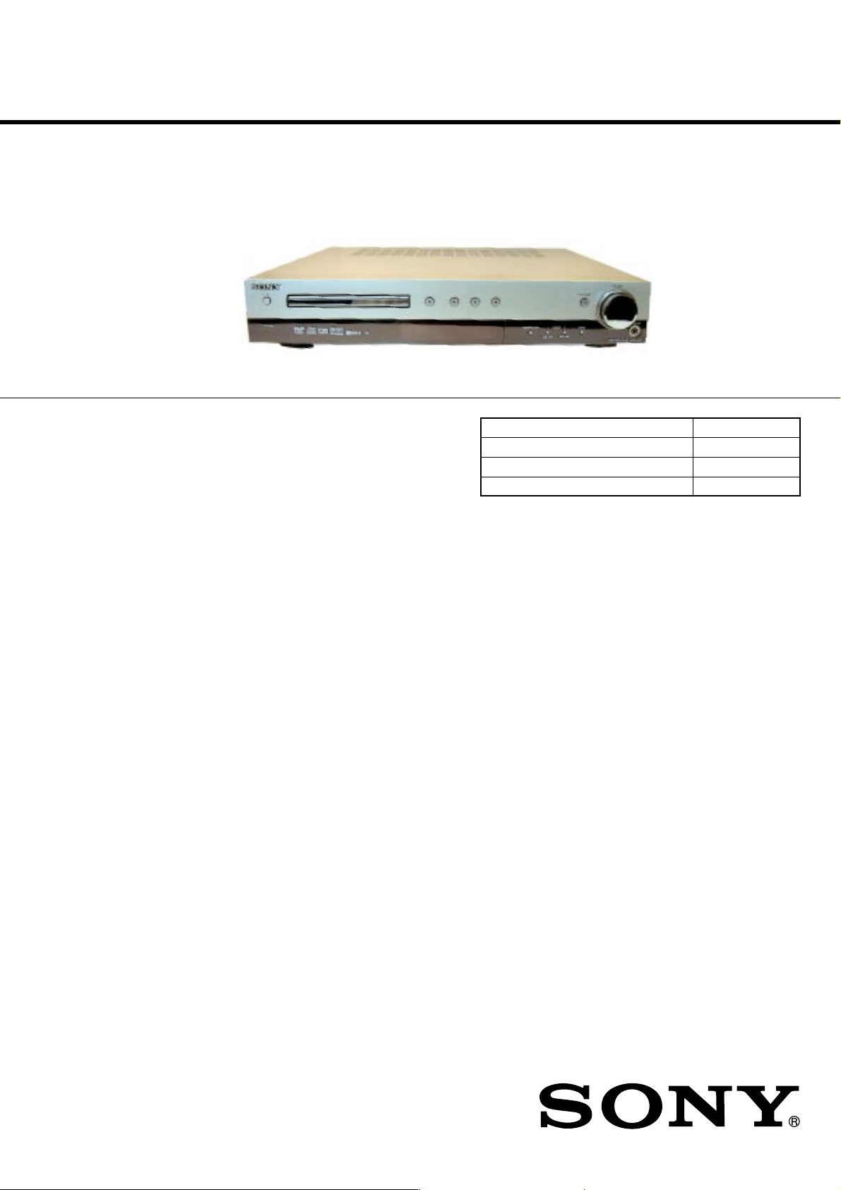
AVD-LS10
SERVICE MANUAL
Ver 1.1 2004. 05
SPECIFICATIONS
Amplifier section
Stereo mode 40 W + 40 W (8 ohms at 1 kHz, THD 0.7 %)
Surround mode Front: 40 W + 40 W (THD 0.7 %)
Center*: 40 W
Rear*: 40 W + 40 W (8 ohms at 1 kHz, THD
0.7 %)
* Depending on the source, there may be no sound output.
Inputs (Analog) VIDEO 1, VIDEO 2, TV-AUDIO:
Sensitivity: 150 mV
Impedance: 50 kilohms
Inputs (Digital) VIDEO 2 (Optical):
Sensitivity: –
Outputs (Analog) VIDEO 1 (AUDIO OUT):
Voltage: 2 V
Impedance: 1 kilohms
SUBWOOFER AUDIO OUT:
Voltage: 3 V
Impedance: 1 kilohms
PHONES:
Accepts low- and high-impedance
headphones
Outputs (Digital) DIGITAL OUT OPTICAL (CD/DVD)
Sensitivity: –
CD/DVD system
Laser Semiconductor laser
(CD: λ = 780 nm, DVD: λ = 650 nm)
Emission duration: continuous
Signal format system NTSC/PAL
Frequency response (at 2 CH STEREO mode)
DVD (PCM): 20 Hz to 20 kHz (+0.5 dB, -3.0
dB)
CD: 20 Hz to 20 kHz (+0.5 dB, -3.0 dB)
Signal-to-noise ratio More than 75 dB (VIDEO 1 (AUDIO)
connectors only)
Harmonic distortion Less than 0.5 %
AEP Model
UK Model
Model Name Using Similar Mechanism NEW
Mechanism Type DP-5RM
Base Unit Name NEW
Optical Pick-up Name NEW
FM tuner section
System PLL quartz-locked digital synthesizer system
Tuning range: 87.5 – 108.0 MHz (50 kHz step)
Antenna FM wire antenna
Antenna terminals 75 ohms, unbalanced
Intermediate frequency 10.7 MHz
AM tuner section
System Tuner section:
PLL quartz-locked digital synthesizer system
Tuning range
North American model: 531 – 1,602 kHz (with the interval set at 9 kHz)
Antenna Loop antenna
Intermediate frequency 450 kHz
Video section (EURO AV)
Outputs Video: 1 Vp-p 75 ohms
General
Power requirements 230 V AC, 50/60 Hz
Power consumption 70 W
1.3 W (in the standby mode)
Dimensions (approx.) 430 x 83 x 355 mm (17 x 3 x 14 inches) (w/h/d)
incl. projecting parts
Mass (approx.) 5.0 kg (11 lb 7 oz)
Operating temperature 5°C to 35°C (41°F to 95°F)
Operating humidity 5 % to 90 %
Supplied accessories See page 14.
— Continued on next page —
AUDIO CD/DVD RECEIVER
9-877-629-02
2004E02-1
© 2004.05
Sony Corporation
Home Audio Company
Published by Sony Engineering Corporaton
Page 2
AVD-LS10
Supplied accessories
• AM loop antenna (1)
• FM wire antenna (1)
• Remote Commander (remote) RM-LS10 (1)
• R6 (size AA) batteries (2)
• Video cord (PINPLUG X 1 y PINPLUG X 1) (1)
Design and specifications are subject to change without notice.
Laser component in this product is capable of emitting radiation
exceeding the limit for Class 1.
This appliance is classified as
a CLASS 1 LASER product.
The CLASS 1 LASER
PRODUCT MARKING is
located on the rear exterior.
This caution label is
located inside the unit.
NOTES ON HANDLING THE OPTICAL PICK-UP BLOCK
OR BASE UNIT
The laser diode in the optical pick-up block may suffer electrostatic
break-down because of the potential difference generated by the
charged electrostatic load, etc. on clothing and the human body.
During repair, pay attention to electrostatic break-down and also
use the procedure in the printed matter which is included in the
repair parts.
The flexible board is easily damaged and should be handled with
care.
NOTES ON LASER DIODE EMISSION CHECK
The laser beam on this model is concentrated so as to be focused on
the disc reflective surface by the objective lens in the optical pickup block. Therefore, when checking the laser diode emission,
observe from more than 30 cm away from the objective lens.
LASER DIODE AND FOCUS SEARCH OPERATION
CHECK
Carry out the “S curve check” in “CD section adjustment” and check
that the S curve waveform is output several times.
CAUTION
Use of controls or adjustments or performance of procedures
other than those specified herein may result in hazardous
radiation exposure.
Notes on chip component replacement
• Never reuse a disconnected chip component.
• Notice that the minus side of a tantalum capacitor may be
damaged by heat.
Flexible Circuit Board Repairing
• Keep the temperature of soldering iron around 270˚C
during repairing.
• Do not touch the soldering iron on the same conductor of the
circuit board (within 3 times).
• Be careful not to apply force on the conductor when soldering
or unsoldering.
SAFETY-RELATED COMPONENT WARNING!!
COMPONENTS IDENTIFIED BY MARK 0 OR DOTTED LINE WITH
MARK 0 ON THE SCHEMATIC DIAGRAMS AND IN THE PARTS
LIST ARE CRITICAL TO SAFE OPERATION. REPLACE THESE
COMPONENTS WITH SONY PARTS WHOSE PART NUMBERS
APPEAR AS SHOWN IN THIS MANUAL OR IN SUPPLEMENTS
PUBLISHED BY SONY.
2
Page 3

TABLE OF CONTENTS
1. SERVICING NOTE ·························································· 4
2. GENERAL ·········································································· 6
3. DIAGRAMS
3-1. Block Diagrams – DVD Section (1/2) – ······················ 9
3-2. Block Diagrams – DVD Section (2/2) – ···················· 10
3-3. Block Diagrams – IN/OUT Section – ························ 11
3-4. Block Diagrams – POWER AMP Section –··············· 12
3-5. Block Diagrams – DISPLAY/POWER Section – ······ 13
3-6. Printed Wiring Board – DVD Section (Side A)– ······· 14
3-7. Printed Wiring Board – DVD Section (Side B)– ······· 15
3-8. Schematic Diagram – DVD Section (1/4) – ··············· 16
3-9. Schematic Diagram – DVD Section (2/4) ·················· 17
3-10.Schematic Diagram – DVD Section (3/4) ·················· 18
3-11.Schematic Diagram – DVD Section (4/4) ·················· 19
3-12.Printed Wiring Board – Main Section (Side A) –······· 20
3-13.Printed Wiring Board – Main Section (Side B) –······· 21
3-14.Schematic Diagram – Main Section (1/5) – ··············· 22
3-15.Schematic Diagram – Main Section (2/5) – ··············· 23
3-16.Schematic Diagram – Main Section (3/5) – ··············· 24
3-17.Schematic Diagram – Main Section (4/5) – ··············· 25
3-18.Schematic Diagram – Main Section (5/5) – ··············· 26
3-19.Schematic Diagram – Panel Section – ······················· 26
3-20.Printed Wiring Board – Panel Section –····················· 27
3-21.Printed Wiring Board – Power Section – ··················· 28
3-22.Schematic Diagram – Power Section – ······················ 29
AVD-LS10
Ver 1.1
4. EXPLODED VIEWS
4-1. Chassis Section ···························································· 31
4-2. Deck Section ······························································· 32
5. ELECTRICAL PARTS LIST ······································· 33
3
Page 4
AVD-LS10
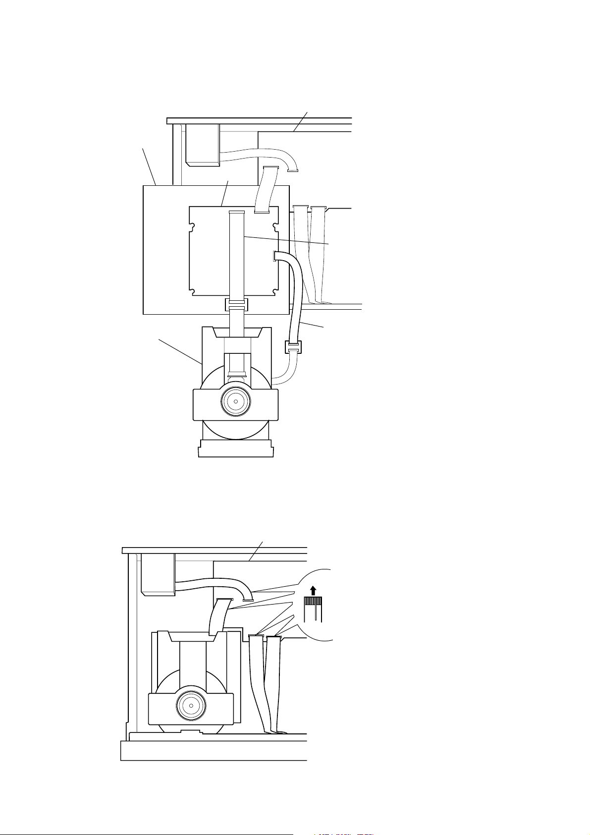
SERVICE POSITION
• DVD MECHANISM
Isolation sheet
SECTION 1
SERVICING NOTE
MAIN BOARD
DVD BOARD
PMD02
Extention Jig: J-2501-245-A (23 core, 300mm)
PMD03
DVD MECHANISM
• NOTE FOR FLAT CABLE CONNECTION
PN103
MAIN BOARD
PN104
PN102
PN101
Extention Jig: J-2501-102-A (13 core, 300mm)
MAIN BOARD
These four flat cables have a direction.
Be sure to connect the side peeled off
the coating to the main board.
In case of connecting the other side
to the main board, the set doesn't operate.
4
Page 5

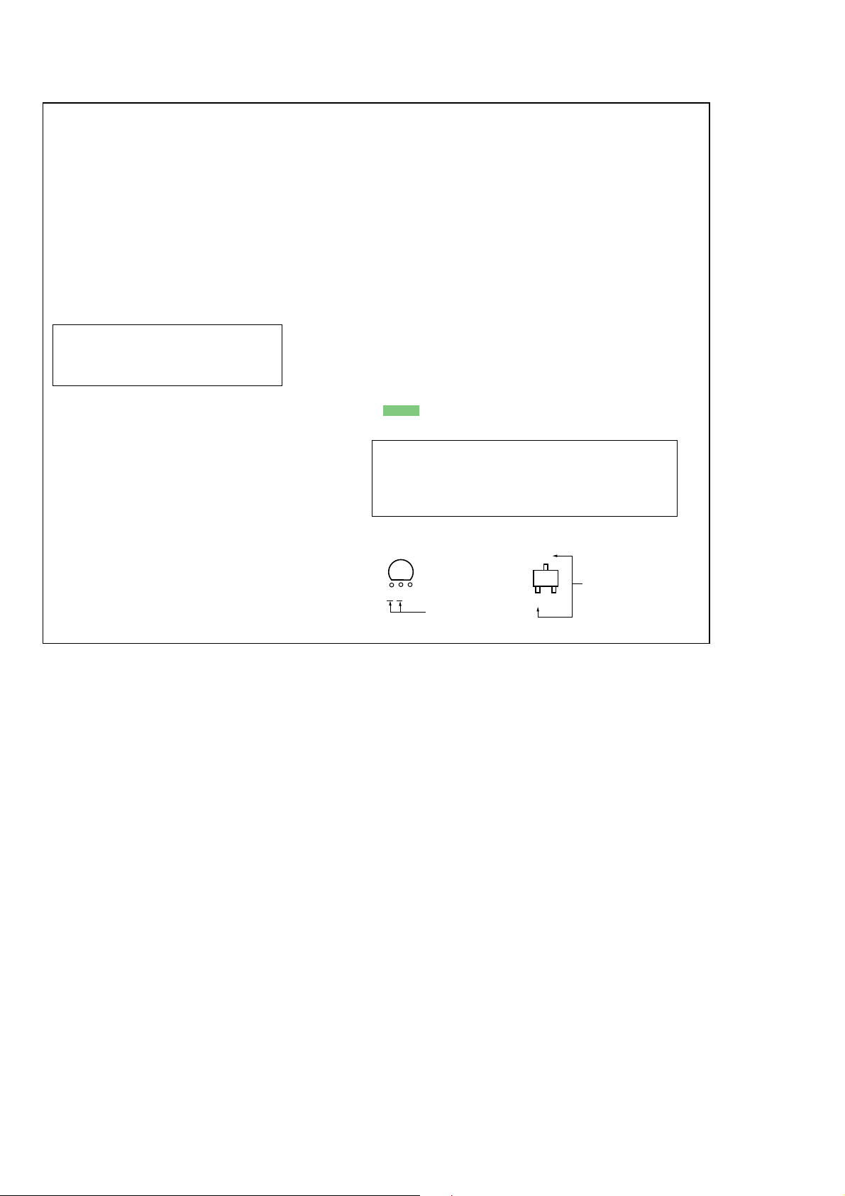
• CLEANING THE OPTICAL PICK-UP
Note 1: In cleaning the lens, do not apply an excessive force
As the optical pick-up is vulnerable, application of
excessive force could damage the lens holder.
Note 2: In cleaning, do not use a cleaner other than exclusive
cleaning liquid. (KK-91 or isopropyl alcohol)
Note 3: Wipe the obujective lens spirally from center toward
outside. (See Figure A)
(Figure A)
AVD-LS10
Ver 1.1
• DISC TRAY LOCK
The disc tray lock function for the antitheft of an demonstration
disc in the store is equipped.
Setting Procedure :
1. Press the \/1 button of the main unit.
2. Put the disc into the tyay.
3. Press two buttons of Z and x simultaneously for five
seconds.
4. The message “LOCKED” is displayed and the tray is locked.
Releasing Procedure :
1. Press two buttons of Z and x simultaneously for five
seconds again.
2. The message “UNLOCKED” is displayed and the tray is
unlocked.
Note : When “LOCKED” is displayed, the tray lock is not released
by turning power on/off with the \/1 button.
5
Page 6
AVD-LS10
Index to Parts and Controls
For more information, refer to the pages indicated in parentheses.
Front Panel
SECTION 2
GENERAL
This section is extracted
from instruction manual.
1 2
I / O
STANDBY MEMORY/CLEAN - +TUNING BAND
34
DIGITAL
PCM
RDS REPEAT 1 ALL
STEREO TUNED
PL II DTS TITLE CHP/TRK
DVD
CD
VCD
MP3
A-B REMAIN MUTEMEMORYPROGRAM SHUFFLE
6
5
ms
dB
MHz
KHz
14
1 POWER switch
2 Disc tray
3 A (open/close)
4 H (play)
5 X (pause)
6 x (stop)
7 FUNCTION
8 VOLUME control
9 PHONES jack
q; BAND
qa TUNING +/–
qs MEMORY/CLEAR
(remote sensor)
qd
qf STANDBY indicator
7
FUNCTION
111213
8
VOLUME
PHONES
DVD RECEIVER AVD-LS10
910
Rear Panel
1 SPEAKERS jacks
2 SUBWOOFER AUDIO OUT jack
3 VIDEO 1/2 jacks
4 MONITOR OUT jack
5 AM antenna
6 FM 75Ω COAXIAL antenna
7 EURO AV OUTPUT (TO TV) jack
8 DIGITAL IN/OUT OPTICAL jacks
6
Page 7
AVD-LS10
This section is extracted
from instruction manual.
Remote
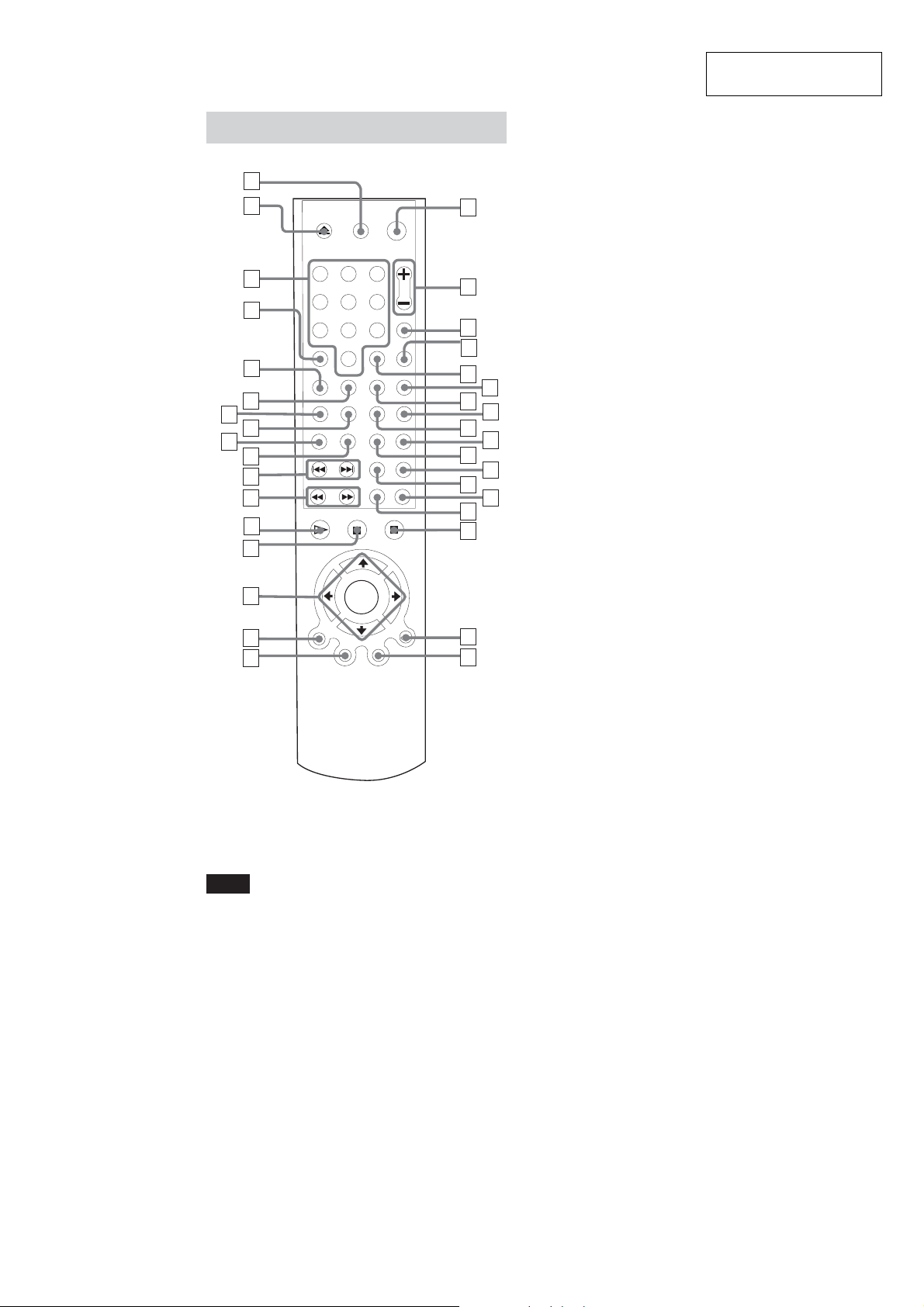
1
2
3
4
5
6
7
8
9
10
11
12
13
14
15
16
17
12
456
78
3
9
0
18
19
20
21
22
24
26
28
30
32
33
34
35
23
25
27
29
31
1 TV [/1 (on/standby)
2 OPEN/CLOSE
3 Number buttons
4 CLEAR
5 FUNCTION
6 BAND
7 PLAY MODE
8 REPEAT
9 DIMMER
0 TEST TONE
qa ./>, PRESET +/–
qs mM SLOW SCAN +/–
qd H (play)
qf X (pause)
qg C/X/x/c/ENTER
qh DVD DISPLAY
qj DVD TOP MENU
qk [/1 (on/standby)
ql VOLUME +/–
w; MUTING
wa TV/VIDEO
ws RDS
wd DOLBY PL/PLII
wf STEREO/MONO
wg 2CHANNEL
wh REPEAT A-B
wj LEVEL
wk DELAY
wl ANGLE
e; SUBTITLE
ea AUDIO
es DVD SETUP
ed x (stop)
ef O RETURN
eg DVD MENU
Note
This remote control glows in the dark. However, before glowing, the remote must be exposed to light for awhile.
7
Page 8
AVD-LS10
d
d
Ver 1.1
THIS NOTE IS COMMON FOR PRINTED WIRING
BOARDS AND SCHEMATIC DIAGRAMS.
(In addition to this, the necessary note is printed
in each block.)
For schematic diagrams.
Note:
• All capacitors are in µF unless otherwise noted. pF: µµF
50 WV or less are not indicated except for electrolytics
and tantalums.
• All resistors are in Ω and 1/
specified.
f
•
• C : panel designation.
• A : B+ Line.
• B : B– Line.
• H : adjustment for repair.
•Voltages and waveforms are dc with respect to ground
•Voltages are taken with a VOM (Input impedance 10 MΩ).
: internal component.
Note:
The components identified by mark ! or dotted
line with mark ! are critical for safety.
Replace only with part number specified.
under no-signal (detuned) conditions.
DVD board section
no mark: DVD STOP
( ) : DVD PLAY
: Inpossible to measure
*
Other board section
no mark: FM
( ) : DVD PLAY
: Inpossible to measure
*
Voltage variations may be noted due to normal production tolerances.
4
W or less unless otherwise
SECTION 3
DIAGRAMS
•Waveforms are taken with a oscilloscope.
Voltage variations may be noted due to normal production tolerances.
no mark : STOP
• Circled numbers refer to waveforms.
• Signal path.
F : FM
J : CD
c : DVD
g : VIDEO
For printed wiring boards.
Note:
• X : parts extracted from the component side.
a
•
• : Pattern from the side which enables seeing.
(The other layers' patterns are not indicated.)
Caution:
Pattern face side: Parts on the pattern face side seen from
(Side B) the pattern face are indicated.
Parts face side: Parts on the parts face side seen from
(Side A) the parts face are indicated.
• Indication of transistor
: Through hole.
CEB
These are omitte
C
Q
EB
These are omitte
8
Page 9
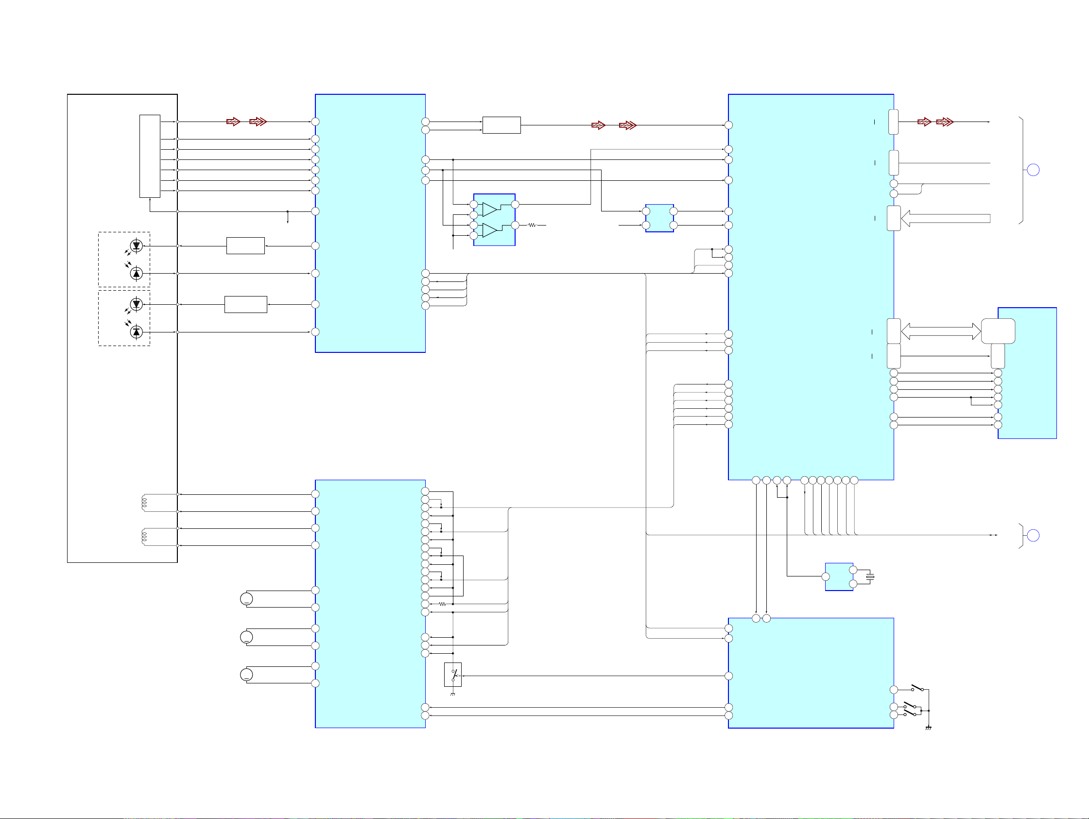
3-1. BLOCK DIAGRAM – DVD SECTION (1/2) –
AVD-LS10
Ver 1.1
OPTICAL PICK-UP
BLOCK
LD (CD)
PD (CD)
LD (DVD)
PD (DVD)
RF
A
B
C
D
DETCTOR
E
BAF
VC INPUT
CD LD
CD PD
DVD LD
DVD PD
Q2A2
CD APC DRIVE
Q2A1
DVD APC DRIVE
VREF1
IC2A1
RF SIGNAL PROCESSOR
3 13
RF IP
52
MA
51
MB
50
MC
47
MD
TRN
55
56
TRP
46
VREF1
41
LD2
40
MD2
LD1
44
43
MD1
EQON
EQOP
TE
PE
FE
SDEN
SDATA
SCLK
MRSTB
MIRR
Q2A5, 2A6
5
+
6
3
+
-
2
IC2A4
ERROR AMP
AMP
7
1
12
36
38
39
VREF1
RF LAT
31
SDATA
30
SCLK
29
/SXRST
28
MIRR
27
RF0
TZC
+5VD +3.3V
5
3
/DSPCS
/RD
/PWEO
IC2A2
BUFFER
7
1
MON
MDP
D REF
FMO
TDO
FDO
VREF
MIRR
SCLK
SDATA
165
RF
TZC
150
TE
CH3
96
FE
93
CH0
EI
CH2
95
97
CH4
69
151
54
53
175
173
174
170
169
79
80
84
88
GPI04
MIRR
E CLK
E SIN
ZCE
ZRD
ZWR
MON
MDP
REF OUT
AOUT2
AOUT1
AOUT0
IC201
CD/DVD DSP
MPEG0
MPEG7
LA0
LA3
A4
A5
PS0
PS7
DATA0
DATA15
ADD0
ADD10
RAS
UCAS
WE
SDRAM CLK
197 - 204
LA0-3
179 - 182
LADD4
183
LADD5
184
187,
AD0-AD7
189 - 195
D0 - 15
1 - 8,
10 - 17
A0 - 10
19 - 23,
25 - 30
33
34
35
OE
36
84
BS
88
RAS
UCAS
SDRAM CLK
BANK SEL
DVD0 - 7
LA BUS
LADDBUS
AD BUS AD
WE
OE
DVD
DATA
LA
LADD
2, 3, 5, 6
8, 9, 11,12
21 - 24,
17
16
15
14
36
35
19
IC203
SDRAM
45,46,48,49
39,40,42,43,
27-32,20
A
TO
DVD
(2/2)
SECTION
(Page 10)
FOCUS
COIL
TRACKING
COIL
IC2M1
MOTOR DRIVER
F+
F-
T+
T-
SPM+
SPINDLE
M
MOTOR
SLED
MOTOR
LOADING
MOTOR
SPM-
FM+
M
FM-
LM+
M
LM-
DO1.2
37
DO1.1
38
DO2.2
35
DO2.1
36
DO3.2
32
DO3.1
33
DO4.2
28
DO4.1
29
DO5.1
27
DO5.2
26
ALL MUTE
OUT1
IN1.2
IN1.1
OUT2
IN2.2
IN2.1
OUT3
IN3.2
IN3.1
OUT4
IN4.2
IN4.1
OPOUT
OPIN(+)
OPIN(-)
MUTE 1.2
MUTE 3
MUTE 4
REV
FWD
46
1
48
47
4
3
2
9
8
5
12
11
10
17
20
21
24
23
22
MUTE SWITCH
15
14
Q2M1
FDO
TDO
FMO
DREF
MDP
MON
ACT MUTE
/S XRST
RF LAT
LOAD OPEN
LOAD CLOSE
82
11
90
4
3
TEST OUT5
46 43
CLK
CDC2PO
77 76
IN SP1
TEST OUT2
59
XTI
SERVO CLK
138
MCK
IC301 (1/2)
MAIN MICOM
ESOUT
GPIO6
60 67
153 105 121 172 152
ESOUT
DSP SENSE
DVD
DEFECT
LOCK
DEFECT
LOCK
IC206
CLOCK OSC
5
SENS
SENS
Z INT
FOK
DSP INT
FOK
1
7
33.8688MHz
MODE SW1
MODE SW2
X201
B
TO
DVD
(2/2)
SECTION
(Page 10)
SYS
CONT
87
85
86
(LIMIT)
(OPEN)
(CLOSE)
• Signal path
J : CD
c : DVD
9
9
Page 10
AVD-LS10
Ver 1.1
3-2. BLOCK DIAGRAM – DVD SECTION (2/2) –
LA0-3
LA
LADD4,LADD5
LADD
AD0-7
AD
DVD(1/2)
SECTION
(Page 9)
A
DVD DATA
DVD0-7
LA BUS
LADD BUS
AD BUS
217,219-223,225,226
IC501
NS PANTERA
SPDIF
CVBS/C
Y/G
C/CB/B
CR/R
68
CVBS
118
Y/Y(G)
114
C/PB
112
PR
110
AD 4-21
IC3F1
SDRAM
15-18,20,22,
23,25,27-30,
32,33,35-37,
39-42
10
DVD SPDIF
C/V
16:9
C
D
POWER AMP
SECTION
(Page 12)
IN/OUT
SECTION
(Page 11)
DVD(1/2)
SECTION
(Page 9)
IN/OUT
SECTION
(Page 11)
AD 0-21
180-178,
176-172,
168-163,
158-157,
155,
153-149
LA0
LA3
184-187
/DSC CS
FOK
DSP INT
SENS
LOCK
DEFECT
DSP SENSE
E SOUT
SCLK
SYS CONT
B
IC502
EEPROM
S DATA
203
XI08
127
VI06
205
XI09
197
XI03
130
VI03
128
VI05
129
VI04
131
VI02
209
XI013
211
XI014
MD0
MD31
200
XI012
193
PCS0
194
XI01
195
XI02
206
XI010
229,231,232,
234-236,238-240,
2,3,5,7,8,9,
43,45,46,48,
CD E OUT
/FLASH CS1
XI01
XI02
XI010
50-52,54-56,
58,61,63,64
LA 0-3
MD0
AD 0-15
LA 0-3
D 0-31
2,4,5,7,8,10,11,
A 0-13
MD13
12,13,15,16,
18,20,21,25,
26,28,29,32,
CSSKDI
EECS
DO
COMM DATA
COMM CLK
F IN
/MRESET
/STROBE
/RD
/PWEO
/PPCS
84
SSP IN1
86
SSP OUT1
87
SSP CLK
81
RSTP
267
XI011
189
RD
182
PWEO
198
XI04
1 432
HDATAO
HDATAI
E
HCLK
/HREQ
/HEST
+
3.3VM
(DVD)
IC506
+
1.8V
REGULATOR
+
1.8V
/HREQ
DQM0
DQM1
DQM2
DQM3
CKE
WE
CAS
RAS
CSO
MCLK
203
127
205
197
130
128
129
131
209
211
33
/DQM0
/DQM1
/DQM2
/DQM3
CKE
/WE
/CAS
/RAS
/CSO
MCLK2
/DQM0
/DQM1
/DQM2
MCLK2
/WE
/CAS
/RAS
/CSO
/DQM3
CKE
IO0
IO15
29-36,
38-45
A0
25-22
A3
13,85,83,82,80,
79,77,76,74,56,
54,53,51,50,48,
47,45,31,33,34,
A0-9
BA0-1
22-27,60-66
16
DQM0
71
DQM1
59
DQM2
68
CLK
17
/WE
18
/CAS
19
/RAS
20
/CS
28
DQM3
67
CKE
A4
A16
CE
IC305
SDRAM
DQ0
DQ31
36,37,39,40,42
21-16,9-1,48
LADD 4,5
LADD 4-21
/FLASH CS0
/FLASH CS1
CD E OUT
/HREQ
/EE CS
XI01
XI02
XI010
40-42,49,50,
52-56,58-61,
63,64
7026
74
72
71
68
81
OUT SP2
95
96
IC301(2/2)
DVD MICOM
/PPCS
/PWEO
93
/DL SW
/RD
/STROBE
AD0-7
PB301
14
13
12
11
2-9
FOR CHECK
1
10
• Signal path
J : CD
c : DVD
g : VIDEO
10
Page 11
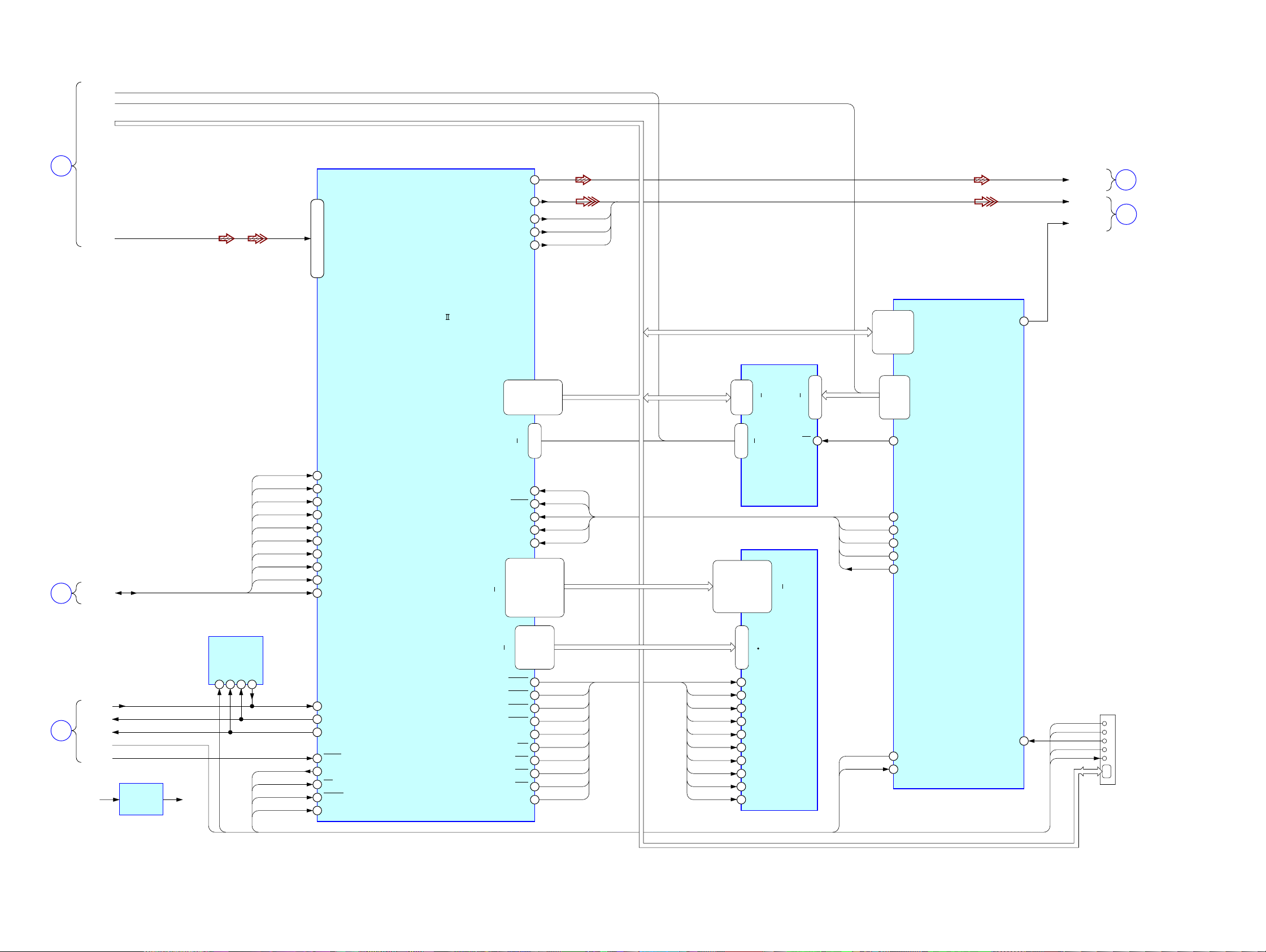
3-3. BLOCK DIAGRAM – IN/OUT SECTION –
TUNER
TUNER-L
VIDEO2
VIDEO1
EURO AV
FM
7552
AM
AUDIO IN
VIDEO IN
AUDIO IN
VIDEO IN
AUDIO OUT
VIDEO OUT
AUDIOSUBWOOFER
VIDEOMONITOR
A OUT R
A IN R
A IN L
SCART CONTROL
R/G/B SELECT
V.OUT(COMPOSITE)
DVD(2/2)
SECTION
(Page 10)
D
TUNER-R
PLL CLK
RDS CLK
RDS DATA
JK601
L
R
L
R
L
R
JK602
1
2
3
6
B
7
8
G
11
R
15
16
19
TMUTE
PLL CE
PLL DI
PLL DO
C/V
16:9
3
5
1
6
7
8
9
11
12
NC
NC
R-CH
R-CH
R-CH
R-CH
C/PB
Y/Y(G)
R-CH
RDS CLK
RDS DATA
CVBS
Q608
RGB SELECT
PR
TMUTE
P CE
P DI
P CLK
P DO
RGB
VIDEO
Q502
MUTE
Q505
MUTE
Q609
BUFFER
16/9
IC502
BUFFER
57
Q501
16:9 SWITCH
Q501.504
MUTE DRIVE
Q504
Q602
IC501
AUDIO SELECT
2
TUNER
3
VCR2
4
VCR1
6
12
COM3
IC102
VIDEO SELECT
V OUT 2
5
V OUT 1
10
V IN 2
3
V IN 1
12
V IN 3
1
+
12V
Q601,603
B+ SWITCH
Q604
TV MODE SWITCH
5
COM1
9
COM2
10
11
17
DATA
16
CK
14
ST
2
SW1
13
SW2
D601
X101
9.8304MHZ
+
5V
DATA
CLK
STB
REC MUTE
SW MUTE
SW1
SW2
15
CF1
16
CF2
77
TV MODE
H/P DET
H/P MUTE
IC503
2 1 2 1
AMP
IC505
7 6 7 6
AMP
TMUTE
HP DET
68
8 3 4 5 6
TMUTE
HP DET
IC504
AMP
IC506
LPF
IC507(2/2)
7 6 1 2
AMP
P DI
P CE
P DO
P CLK
RDS CLK
27 26 81 82
PLL DI
PLL CE
PLL DO
PLL CLK
ANL
ANL
F/L
RDS DATA
REC MUTE
R/M
RDS CLK
RDS DATA
IC101(1/3)
MAIN MICOM
Q902
MUTE DRIVE
+
-
IC507(1/2)
LPF
SW MUTE
H/P MUTE
2
S/M
AMUTE
IC508
3 1
LPF
HP/L
R-CH
R-CH
R-CH
WOOFER
CLK
SW1
SW2
DATA
RGB VIDEO
78 21 22 20 19 10
7312 CLK
2279 SW1
2279 SW2
RGB VIDEO
7312 DATA
SCK
SCLK
LRCK
65
LRCK
R-CH
2
SD IN 2
3
SD IN 1
4
SD OUT
1
SD IN 3
MCLK
10
MCLK
205 CD IN,SCK,LRCK,MCLK
PN105
SDO
SCL
Q101
INITIAL RESET
DATA2
C/W
DATA95
3
DATA96
2
RESET11
6
CLK97
1
Q508
MUTE
R-CH
IC205
SURROUND SOUND,CODEC
25
A OUT 3
26
A OUT 4
+
20
A IN L
-
19
A IN L
+
16
A IN R
-
17
A IN R
23
A OUT 1
24
A OUT 2
28
A OUT 6
CDIN
12
205 CD IN
STB
98
DVD SO
99
DVD SI
100
DVD CK
7312 STB
28
DVD CE
97
DVD RES
11
RESET 5.6V CPU
AVD-LS10
Ver 1.1
JK001
PHONES
XMT958
C/W,DATA2
SDO,SCL
FOR CHECK
HDATA O
HDATA I
HCLK
/HREQ
/HRST
CLOCK
E
• R-ch is omitted due to same as L-ch.
• Signal path
F : FM
J : CD
g : VIDEO
POWER AMP
F
POWER AMP
G
DVD(2/2)
SECTION
(Page 10)
SECTION
(Page12)
SECTION
(Page 12)
11
11
Page 12

AVD-LS10
Ver 1.1
3-4. BLOCK DIAGRAM – POWER AMP SECTION –
IN/OUT
SECTION
(Page 11)
DVD (2/2)
SECTION
(Page 10)
IN/OUT
SECTION
(Page 11)
JK201
OPTICAL
IN
XMT958
F
DVD SPDIF
C
CLOCK
G
OPTICAL
RECEIVER
C/W, DATA2
SCK, LRCK, MCLK, 205 CDIN
SDO, SCL
206 INT
SPDIF MUTE
D O MUTE
2
11
18
9
8415 INT
9702 SDI
505 TH WAR
4
16
WAR
MCLK
Q201
SWITCH
RXP1
12
RXP0
4
RMCK
10
16 17 21 1 28 919
INTEO
6
14
4926 INT
D O MUTE
OSCLK
SCK
SDOOSDI
8
12
+5V
IC206
DIGITAL AUDIO
INTERFASE/RECEIVER
OLRCK
OMCK
INT
206 INT
CK1
LRCK
IC207
BUFFER
CDOUT
SDOO
SDOUT
CCLK
SCL
IC208
BUFFER
18
RST
206 RST
SCD OUT
493SDI
14
6119
493SDO
Q203
SWITCH
SPDIF MUTE
DATA2
505 PDNO
18
2
505PDN
3
3
22
27
3
17
9702SDO
OPTICAL
TRANSMITTER
XMT958
DTS DECODER
SDATA IN
SDATA IN 2
SCLK IN 1
LRCK IN 1
SCLK IN 2
25 26 28 7 36 3029
LRCK
SCK
SCL
205 CDIN
SD OO
SCL
7
5
13
15
SCL
SDO
IC201
AC-3/
LRCK IN 2
LRCK
SCL
205 RST
206 RST
AUDATA 0
AUDATA 1
AUDATA 2
7SCCLK
JK202
OPTICAL
RESET
116
84
OUT
SCLK
LRCK
MCLK
CK0
9702 PDN
41
40
39
43
42
44
CLK IN
9702 RST
C/W
9702 SCL
CEN PD
75878586849596887371657976 91 71 93 94
SCK
LRCK
MCLK
SDO
SCL
FRONT
REAR
C/W
SCK
LRCK
INTEO
SCDOUT
9702 SCL
9702 RST
9702 PDN
CK2
505 FAULT
D301
17
21
26
22
23
79
20
19
80
92
4
86
76
SSDIN0
SSDIN1
SSDIN 2
SDCK 1
SLKCK 1
SO/SDA
INTEO
SCDOUT
SCK/SCL
/RESET
PLL PDN
CLK IN
O/L
IC301
DIGITAL AUDIO
PROCESSOR
PWM2+
PWM2-
PWM1+
PWM1-
PWM4+
PWM4-
PWM6+
PWM6-
PWM5+
PWM5-
IC710
POWER AMP
IN 2B
56
57
53
54
505TH WAR
505 FAULT
505 PDNO
63
64
505TH WAR
505 FAULT
CEN PD
70
71
67
68
505TH WAR
505 FAULT
505 PDNO
32
31
30
29
28
27
26
25
32
31
28
27
26
25
32
31
30
29
28
27
26
25
IN 2A
IN 1B
IN 1A
TH WAR
FAULT
TRISTATE
PWRON
POWER AMP
IN 2B
IN 2A
TH WAR
FAULT
TRISTATE
PWRON
IN 2B
IN 2A
IN 1B
IN 1A
TH WAR
FAULT
TRISTATE
PWRON
IC750
IC730
POWER AMP
OUT 2B
OUT 2B
OUT 2A
OUT 2A
OUT 1B
OUT 1B
OUT 1A
OUT 1A
OUT 2B
2
3
OUT 2B
8
OUT 2A
OUT 2A
9
OUT 1B
10
OUT 1B
11
OUT 1A
16
OUT 1A
17
BIAS +3.3V
23
VCC
OUT 2B
2
3
OUT 2B
8
OUT 2A
OUT 2A
9
BIAS
23
VCC
2
3
8
9
10
11
16
17
BIAS
23
VCC
+32.5V
+3.3V
+32.5V
+3.3V
+32.5V
JK700
+
-
+
-
+
-
+
-
+
-
L
FRONT
R
CENTER SPEAKER
L
SURROUND
R
D O MUTE
SPDIF MUTE
8415 INT
9702 SDI
4926 INT
505 TH WARN
4228 SDI
4926/8415/
IC101 (2/3)
MAIN
MICOM
493 SDI
493 SDO
505 PDN
9702 SDO
4228 SCL
4926/8415/
4228 SDO
4926/8415/
4228 RST
4926/8415/
9702 RST
9702 PDN
12
CEN PD
9702 SCL
12
CK 0
CK 1
X201
12.288MHz
CK 2
505 PDNO
• Signal path
F : FM
J : CD
Page 13

3-5. BLOCK DIAGRAM – DISPLAY/POWER SECTION –
-12V
+32.5V
+8V(DVD)
+12VA
+5V
+5V(DVD)
+3.3V
+3.3VM(DVD)
+8V REGULATOR
+3.3V REGULATOR
IC962
IC965
IC971
-12V REGULATOR
IC961
+12V REGULATOR
IC963
+5V REGULATOR
IC964
+3.3V REGULATOR
D936 RECT
D931
RECT
D933
RECT
D934
RECT
D935
RECT
T901
POWER SWITCHING
TRANFORMER
MAIN
F902
D902,911
AVD-LS10
Ver 1.1
1
5
2
LD001
STANDBY
RMC001
RMC
RECEIVER
KEY NETWORK
SW002-009
LED DRIVER
VR001
VOLUME
SW011
SW010
Q002
D102
+5.6V CPU
RMC
29
KEY1
12
KEY2
18
STBY LED
9
VOL UP
70
VOL DN
69
IC101(3/3)
MAIN MICON
P1
P16
PWR SNS
OPTION
42-45
G1
G9
VP
P CTL
VDD
60
47-50
52-59
30-41
51
26
80
D001-007
SEG1-16
GD1-12
VFD001
FLUORE SCENT
INDUCTOR TUBE
SEG5-11
SEG1
20-5
SEG16
GD1
38-27
GD12
+5.6V CPU
V1
421(-27.5V)
V2
+5.6V CPU
MUTE 5V
(-23V)
(-34V)
D955 D953
Q972,974
-23V REGULATOR
Q982,973
BUFFER
D954
Q950
PROTECT
Q971,975
-34V REGULATOR
IC972
POWER DETECT
IC951
SHUNT REGULATOR
1
SHUNT REGULATOR
D941 RECT
D952 RECT
D951
3
2
ISOlATION BUFFER
3
IC952
2
POWER SWITCHING
F903D942 RECT
ISOlATION BUFFER
1
D912
ISOlATION BUFFER
1
2
TRANFORMER
1
2
1
2
4
3
PC910
T902
SUB
4
3
PC920
4
3
PC921
D921
4
3
IC901
SWITCHING
REGULATOR
A1268
START SWITCH
81
D922
7
2
IC902
SWITCHING
REGULATOR
3
4
5
6
BD901
RECT
LF901 LF902
PD901
AC IN
F901
13
13
Page 14

AVD-LS10
Ver 1.1
3-6. PRINTED WIRING BOARD – DVD SECTION (SIDE A) –
1
A
DVD BOARD (SIDE A)
2
3 4 5 6
R2P1
11
10
1
2
PMD03
• Semiconductor
Location
Ref. No. Location
D201 D-3
D2A1 C-2
D2A2 D-2
D2A3 E-2
C536
C524
C518
C519
IC203
C534
C535
IC501
C295
C293
C533
C520
L206
C521
R522
R523
R521
25
1
R350
C540
2
1
C532
C541
R353
R351
R505
C543
R352
C531
C522
R591
C3F1
L3F1
R354
R590
L301
C302
181
120
R589
25
48
R355
R356
R506
C539
R309
1
25
C3F2
R357
14
180
121
R504
R588
C301
100
R358
R359
15
C530
C529
26
C303
R3F4
R360
C528
C527
C526
C525
C503
R317
R306
IC301
IC3F1
R3F3
R362
P3301
C306
R363
R307
R597
R308
C304
R501
R367
R366
76
R310
50
R3F2
R365
R3F5
R364
75
51
R368
C305
24
1
R318
R319
R320
R303
R302
R3F1
R321
C316
IC201 E-4
IC203 E-5
IC206 D-4
IC2A1 E-2
IC2A2 D-2
IC2A4 E-2
IC2M1 C-2
IC301 D-6
IC305 B-4
IC3F1 E-6
IC501 B-5
IC502 B-2
IC506 B-3
Q2A1 C-2
Q2A2 D-2
Q2A5 E-2
Q2A6 E-2
Q2M1 C-2
4
1
R2P3
8
5
R202
R2F6
C2C4
C2C8
R2C5
R2C4
R2D5
D2A3
R2F2
R2F4
R2F3
C544
R2P8
R2Q1
13
12
48
C2N1
L2A1
IC506
2
C2N4
R2N4
R2N3
R2N2
R2N0
R2M9
R2M7
R2M6
R269
C538
R2P9
R2P0
1
R535
C551
R533
R532
B
MAIN
1
C555
2
BOARD
(Page 20)
R539
C553
A
P5501
22
23
R2B2
R2B3
Q2A1
BCE
2
C2D3
R2B7
Q2A2
C2E3
R2D9
R2D8
C2C3
22
R2B6
BCE
C2E2
C2A6
49
64
R2B1
C2D6
R2A1
PMD02
R2D6
10
R2E9
R2B9
1
4
C2D2
L2A2
R2B5
C2C6
R2G3
C2C1
R2F5
48
IC2A1
C2A7
C2A8
D2A1
C
R2B0
R2B4
1
OPTICAL
PICK-UP
BLOCK
23
R2B8
D
D2A2
C2C2
C2E4
R2D2
R2D1
R2C9
R2C8
R2C7
R2C6
C2B0
C2D9
C2A5
E
R531
C554
R534
C2M9C2M8
R2F8
R2F9
C2A9
C2A3
C2D7
C202
33
16
R2A6
Q2A6
C2B3
8
5
5
8
C552
R537
Q2M1
BCE
25
C2M7
36
IC2A2
R203
1
4
R204
R2G1
32
17
C2B5
Q2A5
IC502
C542
L505
R536
C2M6
24
R2P2
IC2M1
37
R2F7
R2G4
C2C7
R2G2
R2G7
R2E8
C2B4
R2E6
BCEBCE
R2E7
R2F1
C2B8
R2D0
R2A9
R2C0
C2B9
R2M3
D201
C260
L201
3
1
R2P7
R2M2
L203
C240
C207
L504
C2N3
R2N7
R2N6
R2N5
R2N1
C2M5
R2M8
C2M4
C2M3
R2M5
C2M2
R2M1
C230
L503
R282
C208
C209
L207 C229
105
C231
C214
R252
156
R276
IC2A4
C309
L502
C205
C215
C238
C320
C319
L302
C318
C273
104
157
R217
C523
R278
C245
R277
1
43
C506
C210
R201
C286
R275
R279
C239
R279
IC305
C226
C258
IC201
C242
R218
R274
C225
R219
C255
C201
R220
C254
C216
86
C307
C314
44
C253
C251
R229
IC206
C252
C206
C224
4
5
R241
R236
R234
R232
R230
C510
C511
R525
1
R291
53
208
C509
L506
C512
C513
C514
C515
C516
C517
8
C292
52
R290
C290
R207
C291
1
R281
R239
C204
C203
R2N8
1
60
R237
R235
R233
R231
R2N9
240
61
C508
R242
R243
R240
26
C296
C294
50
FOR
F
14
14
CHECK
Page 15

3-7. PRINTED WIRING BOARD – DVD SECTION (SIDE B) –
AVD-LS10
Ver 1.1
1
2
3 4 5
POWER
BOARD
B
P5101
(Page 28)
112
C308
C317
C504
DVD BOARD (SIDE B)
A
B
C501
C507
C2M1
C2D0
C204
C205
X501
C
X201
C212
C213
D
C261
C264
C263
E
C262C265
C272
C274
C287
C280
C211
C288
C232
C278
C284
C2C9
C2A0
C2D1
C2C2
C2A4
C285
C281
C279
F
15
15
Page 16

AVD-LS10
Ver 1.1
3-8. SCHEMATIC DIAGRAM – DVD SECTION (1/4)– • See page 30 for waveforms.
L2A2
HB
C2D6
0.1
C2M1
100
16V
R2M1 1k
R2M8 1k
C2M2
6800P
R2M5
51k
C2M3
4700P
R2M2 10k
R2M9
C2M4
0.1
R2N1
1k
C2M5
0.1
R2N4 15k
R2N5 12k
R2M6
10k
10k
R2N2
5.6k
R2N6 1k
R2N7 1k
R2M3
7.5k
R2M7 10k
R2N0 12k
R2N3
10k
R2P0
4.7k
R2P8 1.2k
R2P9
4.7k
C2N1
0.1
IC2M1
KA3032
MOTOR DRIVER
R2P7
22k
C2N3
0.022
R2Q1
C2N4
10k
2.2
Q2M1
KRC103S
MUTE
SW
C2M
0.1
OPEN SW
CLOSE SW
LIMIT SW
RP2P
10k
R2P3
10k
ITCH
6
R2N9 10k
R2N8 10k
R2P1 10k
C2M9 0.1
C2M7 0.1
MDP
MON
C2M8 0.1
FDO
TDO
FMO
LOAD CLOSE
LOAD OPEN
ACT MUTE
D VREF
(Page19)
(Page18)
(Page17)
T+
R2
R2
C2D2
0.1
CD LD
CD PD
F-
F-
D8
D9
VCC
20
5.6K
56K
GND
CD LD
A3
D2
R2D5 6.8k
R2B0
1k
CD PD
R2D6
91
VOL(LCD)
PMD02
23
DAN202K
R2B1
B
5V D
C
B
A
F
E
5.6k
R2D4
R2B3
18
VREF1
R2E8 0
D2A1
DAN202K
0
0
R2D1
R2D2
5.6k
5.6k
R2C6
R2C7
HD153702TF
RF SIGNAL
PROCESSOR
R2C4 1k
C2
C2
R2B4
0
C2D0
47
16V
1k
5.6k
5.6k
R2C8
R2C9
IC2A1
R2C5 1k
B9
C3
R2B2
18
0.1
0.1
5.6k
R2D3
Q2A1
2SA1037K
DVD APC
DRIVE
R2B5
1k
CD PD
C2D1
47
16V
EQOP
R2B6
18
R2B8
0
R2F8
R2F9
R2G1
R2G2
Q2A5
KTC3882
AMP
C2C1
C2C2
R2F5
C2C9
10
16V
R2F1
220
0.1
10 16V
22k
2.2k
2.2k
2.2k
2.2k
C2C8
0.1
R2B7
18
Q2A2
2SA1037K
CD APC
DRIVE
R2F2
220
R2F3
100
R2G7 10k
5.6k
R2G4
RFO
R2F4
100
R2G9
150
1000p
1000p
C2C4
C2C6
5.6k
5.6k
R2F6
R2G3
D2A2
DAN202K
L2A1
Q2A6
KTC3882
AMP
3300p
C2C5
DVD PD
5.6k
R2F7
RF LAT
S DATA
S CLK
/S XRST
MIRR
FE
PE
TE
C2D3
0.1
EQON
C2A0
47
16V
D
BAF
C
D
A
E
A
0.068
0.1
1500P
0.1
12K
3900P
100
100
0.068
0.033
15
T-
T+
B
F+
D
C
R2A9
56k
R2C0
5.6k
C2D7
1500P
10
E
A5
A7
A8
A9
A6
B3
E7
E6
B4
B5
VCC
VC INPUT
GND
DVD LD
VOL(DVD)
VCC(HF)
DVD PD
RF
5
1
DVD LD
DVD PD
R2A1
C2D4
16V
FF+
TT+
47
1000P
A6
C2
EQOP
EQON
VREF1
TZC
DVD LD
CD LD
91
C2A4
10
16V
C2A3
0.1
R2B9
IC2A4
KIA393F
5.6k
VREF
C2D5
10
16V
C2D9
0.1
R2D0
5.6k
F
C2
C2
C2
C2
R2
C2
R2
R2
C2
C2
T-
F+
B
PMD03
GND
GND
SW(LEAD IN)
LM+
SW(OPEN)
SW(CLOSE)
LM-
FM-
FM+
SPM-
SPM+
M GND
(Page17)
8V
A.GND
16
16
Page 17

3-9. SCHEMATIC DIAGRAM – DVD SECTION (2/4)– • See page 30 for waveforms.
AVD-LS10
Ver 1.1
C504
(Page18)
10
16V
3.3V M
IC506
BA18BCOFP
+1.8V REG
R521
4.7k
R522
10k
R523
4.7k
C506
2.2
/PWEO
E ENB
(Page19)
L502
/RD
A GND
L503
L504
C501
16V
C507
16V
COMM CLK
COMM DATA
F IN
/MRESET
C524
0.1
C518
C519
0.1
0.1
SPDIF
/DQM3
MD31
MD30
MD29
C517
0.1
L506
R525
MD28
MD27
MD26
MD25
MD24
MD23
MD22
MD21
MD20
MD19
MD18
MD17
MD16
/DQM2
/DQM0
/WE
/CAS
/RAS
/CSO
MA13
MA12
MA10
MA0
MA1
MA2
CKE
180
MCLK2
MA3
MA4
MA5
MA6
MA7
MA8
MA9
/DQM1
MD15
MD14
MD13
MD12
MD11
MD10
EE CS
COMM CLK
COMM DATA
F IN
C516
0.1
C515
0.1
C513
0.1
C514
0.1
C512
0.1
C511
0.1
C510
0.1
C509
0.1
C508
0.1
CVBS
Y/Y/G
C/PB/B
R588
R589
75
75
R590
R504
100
C503
47
C538
2.2
C523
47
2.2
FOK
DEFECT
DSP SENSE
LOCK
E SOUT
E DR
E ENB
C525
0.1
C526
0.1
AD21
AD20
AD19
AD18
AD17
AD16
AD15
AD14
AD13
AD12
AD11
AD10
AD9
AD8
AD7
AD6
AD5
AD4
AD3
AD2
AD1
AD0
R501
3.3k
C527
C528
C529
0.1
0.1
0.1
AD4
0.1
R506
1k
CVBS/PR/R
R591
75
75
R505
C543
10
C540
18p
X501
C541
27MHz
27p
C522
0.1
0.1
R597
0
C521
IC501
NDV8602
C520
0.1
0.1
IC502
SPDIF
COMM CLK
COMM DATA
F IN
/HREQ
/MRESET
VIDEO SW
16:9
C/PB/B
CVBS/PR/R
Y/Y/G
CVBS
3.3V M1
R531
R532
R533
R534
R535
R536
R537
R539
1.2k
1.2k
1.2k
1.2k
1.2k
1.2k
1.2k
10k
C542
0.1
0.1
C551
L505
220p
C552
220p
C553
220p
C554
C544
2.2
220p
C555
B
5V D
D GND
3.3V
M GND
8V
A.GND
P5101
P5501
1
5
10
15
20
23
(Page16)
(Page18)
(Page19)
(Page18)
(Page16)
(Page29)
(Page19)
(Page25)
C530
0.1
/PWEO
LA0
ALE
LA2
LA1
LA3
/FLASH CSI
/RD
C531
XIO1
/PP CS
XIO2
SENSE
0.1
C532
0.1
MPEG ERROR
/DSP CS
XIO10
DSP INT
CD E OUT
/STROBE
C533
0.1
S CLK
S DATA
C534
0.1
PSYNC
REQZI
SDCLKI
ZISENB
17
DVD0
DVD1
DVD2
DVD3
DVD4
C535
0.1
DVD5
DVD6
DVD7
MD0
17
MD1
MD2
C536
MD4
MD5
MD6
MD7
MD8
MD9
MD3
0.1
Page 18

AVD-LS10
Ver 1.1
3-10. SCHEMATIC DIAGRAM – DVD SECTION (3/4)–
(Page16)
(Page17)
(Page19)
FOR
CHECK
P3301
5V D
C304
0.1
7
D17
LADD
LAD
LADD18
LADD19
LADD8
LADD9
LADD10
LADD11
LADD12
LADD13
C305
0.1
R321
1k
C316
0.1
10k
R350
100
R351
R352
R353
R354
R355
R356
R357
R358
R359
R360
R361
R362
R363
B
/STROBE
100
AD0
100
AD1
100
AD2
100
AD3
100
AD4
100
AD5
100
AD6
100
AD7
100
/RD
0
/DL SW
100
/PWEO
100
/PP CS
LADD14
LADD15
LADD16
/FLASH CSI
/FLASH CSO
XIO10
XIO2
XIO1
R320
4.7k
R303
R319
4.7k
0
R318
4.7k
0
R365
C2PO
CD
D10
M
D11
M
C306
0.1
D12
M
0
R366
CD E OUT
0
364
R
CLK
C307
0.1
9
D8
D
M
M
1k
R367
ST
/S XR
C314
0.1
D13
M
D14
M
LADD6
4
D5
AD21
LADD
LAD
HS353106HYNIX
DVD MAIN MICOM
1k
1k
1k
310
307
R
R
R308
SE SW
IT SW
CLO
OPEN SW
LIM
D15
M
IC301
1
QM
/D
C301
0.1
AD20
AD19
UTE
ACT M
AD18
CLK2
M
4.7k
306
R
CKE
AD17
10k
317
R
/DL SW
A9
M
C303
0.1
AD16
VIDEO SW
/HREQ
A8
A7
M
M
AD15
EE CS
A6
M
AD14
A5
M
10k
R309
C302
L301
2.2
L3F1
13
AD
AD12
LADD15
LADD14
LADD13
AD11
AD10
AD9
AD8
AD7
AD6
AD5
AD4
ALE
RF LAT
16:9
LOAD OPEN
LOAD CLOSE
2
A4
A3
M
M
QM
/D
18
16
17
D
D
D
M
M
M
D19
M
22
D21
M
23
D
D
M
M
20
D
M
LADD12
LADD11
LADD10
LADD9
LADD8
LADD19
/PWEO
LADD18
LADD17
LADD7
LADD6
LADD5
LADD4
LA3
LA2
LA1
R3F5 10k
R3F2 1k
IC3F1
MBM29LV800BA-90PFTN
SDRAM
LADD16
/FLASH CSO
AD15
AD7
AD14
AD6
AD13
AD5
AD12
AD4
AD11
AD3
AD10
AD2
AD9
AD1
AD8
AD0
LA0
C3F1
2.2
C3F2
0.1
R3F4
10k
/RD
(Page17)
(Page17)
(Page19)
3.3V M
D GND
3.3V
C309
L302
33uH
C317
C308
2.2
47
16V
47
16V
0
1
2
D
D
D4
D
D3
D5
D6
M
M
M
M
M
D7
M
M
M
C320
0.1
IC305
HY57V652220
SDRAM
0
E
AS
QM
/D
/W
/CAS
A12
A13
/R
/CSO
M
M
C319
0.1
3
QM
A10
A1
A0
A2
M
M
/D
M
M
18
24
D
M
C318
0.1
26
25
D
D
M
M
D27
M
30
D29
M
31
D
D
M
M
28
D
M
18
Page 19

3-11. SCHEMATIC DIAGRAM – DVD SECTION (4/4)– • See page 30 for waveforms.
L203
DVD6
DVD7
DVD4
DVD5
DVD2
DVD3
DVD0
DVD1
C265
16V
C295
C264
16V
C293
PSYNC
ZISENB
R290
SDCLKI
MPEG ERROR
0
D201
C261
C284
10
47
6.3V
16V
L206
IC203
ICDATA00
ICDATA01
ICDATA02
ICDATA03
10
ICDATA04
ICDATA05
0.1
ICDATA06
ICDATA07
OE
E
W
UCAS
10
RAS
BANK SEL
0.1
ICADDR10
ICADDR0
ICADDR1
ICADDR2
ICADDR3
IC2A2
BUFFER
ICDATA15
ICDATA14
ICDATA13
ICDATA12
ICDATA11
ICDATA10
ICDATA09
ICDATA08
SDRAMCLK
ICADDR9
ICADDR8
ICADDR7
ICADDR6
ICADDR5
ICADDR4
R202
0
C262
10
16V
C296
0.1
C263
10
16V
OE
C294
0.1
PI
PE
C232
10
10V
ICDATA00
ICDATA01
ICDATA02
ICDATA03
ICDATA04
ICDATA05
ICDATA06
ICDATA07
ICDATA08
ICDATA09
ICDATA10
ICDATA11
ICDATA12
ICDATA13
ICDATA14
ICDATA15
ICADDR0
ICADDR1
ICADDR2
ICADDR3
ICADDR4
ICADDR5
ICADDR6
ICADDR7
ICADDR8
ICADDR9
ICADDR10
BANK SEL
RAS
UCAS
E
W
OE
SDRAM
C203
0.1
C204
0.1
CLK
CDC2PO
CLK
REQZI
AD7
100
R237
AD6
100
R236
AD5
100
R235
AD4
100
R234
100
R233
AVD-LS10
Ver 1.1
R218
470
R219
C201
10k
0.1
R220
C216
10k
0.1
MDP
VREF
AD3
AD2
AD1
AD0
100
100
100
R231
R232
R230
/S XRST
1k
R229
LADD5
IC201
LADD4
LA3
LA0
LA1
LA2
/PWEO
/DSP CS
/RD
DSP INT
MON
6.3V
10
C278
6.3V
10
C279
0.1
C239
RFO
6.3V
10
C285
L201
0.1
C286
2200p
C240
C207
1
R277
R217
C245
R275
R273
1.5k
C242
0.1
C238
1.5k
A GND
C280
10
0.1
R274
6.3V
620
MIRR
R252
SENSE
FOK
TZC
MCK
CNIN
C215
0.1
C214
0.1
C208
0
0.1
C209
0.1
DEFECT
(Page17)
1
150
R276
910
10
C281
10
6.3V
(Page17)
(Page18)
R204
VREF
R203
1k
C202
0.1
1k
1
C254
D VREF
FMO
1
C225
TDO
19
1
C226
1
6.3V
6.3V
6.3V
C258
0
10
10
10
C212
C211
C213
R201
R279
0
FDO
FE
C210
0.1
C273
0.1
0.1
6.3V
10
C288
C230
C231
6.3V
10
C287
C205
0.1
2.2
R278
0
TE
PI
VREF
D GND
0
0
0
0
0
0
R281
R239
R240
R243
R242
R241
S CLK
S DATA
E DR
E ENB
3.3V
L207
C206
E SOUT
MCK
0.1
C224
CNIN
DSP SENSE
MIRR
0.1
1
C251
C272
C255
6.3V
10p
C252
47
0.1
1
C253
19
C229
C290
18p
0.1
LOCK
X201
33.8688M
C274
47
6.3V
IC206
04FU
TC7W
CLOCK OSC
Hz
R207
1M
R291
C291
5V D
MCK
0
C292
0.1
18p
B
(Page16)
(Page17)
(Page18)
Page 20

AVD-LS10
Ver 1.1
3-12. PRINTED WIRING BOARD – MAIN SECTION (SIDE A) –
3 4 5 6 7
L305
L306
L307
C314
R324
R323
R310
R752
R345
100
R311
C751
C312
R321
R318
R316
C309
C308
R317
R314
R346
R312
C318
R753
L308
R750
R313
C752
R754
C317
R322
C310
C325
R319
R320
R793
C315
R307
R306
L750
C324
R308
C754
C313
1
R309
19
IC750 IC730
18
C769
R768
C769
R713
C713
C710
2
L710
L304
L770
C307
L303
C988
C302
C303
C322
C321
C306
C326
C304
C305
26
C316
R331
R330
R332
R328
R329
R327
R326
R325
25
IC301
50 76
51 75
C310
C320
R304
R301
R302
R303
R305
R791
R790
1
A
MAIN BOARD (SIDE A)
B
C714
C711
R712
C712
R711
R714
C
19
36
IC710
18
C727
C725
D
C717
1
C715
C719
R718
E
R728
C729
R727
C728
R717
C718
R315
R792
L302
C753
1
36
C750
L310
L202
C756
R748
R215
R217
R216
C745
R220
C734
19
18
C201
R767
R732
R733
C731
C747
R731
C758
C215
R734
L205
L204
R231
R232
R233
C210
C212
R234
R235
C732
36
1
C733
C730
C737
R747
C748
L203
L730
C735
R734
29
39
R236
C982
28
40
R237
C738
R238
R739
R239
C739
FB509
IC201
44
R242
R241
R240
FB507
8
9
• Semiconductor
R544
C567
D
PN102
R144
8
1
R535
R281
C216
(Page 27)
L101
5
IC503
4
C521
R533
R531
L216
PANEL
BOARD
R116
C109
R160
C518
C517
R519
5
8
C569
R513
R515
R285
1
R582
R580
R581
R136
R137
R138
R135
L105 L104
C570
4
1
IC502
R517
R516
L214
C242
R583
R139
R518
R140
R520
C513
FB604
R284
R141
R514
R605
C515
R621
R142
C514
R622
R123
R593
C581
D601
R591
FB510
R592
R594
C582
R587
C576
IC508
R585
C580
1
R525
C584
C594
4
R599
R549
R547
C537
R551
C541
R555
R553
C543
8
C551
R545
1
2
C605
R603
R565
R614
R613
FB607 FB609 FB608
FB511
R557
R559
R561
C547
R610
C549
R611
R563
C608
R604
C612
IC505
5
8
L601
R606
8
5
IC506
5
R612
C617
C606
C583
1
PN103
14
1
4
C538
R556
R554
C544
4
C552
R558
1
IC102
R615
C593
R598
R586
R585
R584
C579
R500
R546
R560
R122
C619
R548
R550
R552
C542
R562
C548
7
A
23
22
R564
R566
R608
R609
R620
R589
R609
R619
C604
R607
R588
R617R618
8
DVD
BOARD
(Page 14)
PANEL
BOARD
C
(Page 27)
IC504
C5423
R527
16
R522
30
R512
R530
R508
R506
C504
R502
C502
R504
C104
C532
C103
R538
8
1
R537
IC501
1
R115
C524
C508
E
R163
5
4
24
R112
R108
R107
R111
R106
R110
R109
R105
C531
R501
C243
Q102
L103
R162
R161
R101
R130
R143
R536
1
FB501
15
C501
R532
R511
R503
R534
C507
C217
C522
R539
R528
R521
R529
C568
R543
23
31
100
R147
R121
10
C231
R267
C233
R270
R268
30
1
R120
R509 R579
R119
R104
R103
R102
R114
R118
R541
R540
C530
R542
C503
R507
PN101
R113
L209
R526
R505
L106
FB508
L201
C203
R230
R206
L102
R229
R227
R228
R225
18
R214
17
R213
7
1
6
R204
R203
R202
R201
C208
C220
C223
R245
R244
C558
R571
R569
R573
R572
R570
R578
R577
FB602
FB601
L208
FB502
R212
R211
C205
R210
R209
R208
R207
FB605
L213
L212
R150
L207
R226
R282
R347
R567
C561
R159
11
20
5
R132
R131
C240
R264
R263
R262
R261
R260
R269
L210
R252
R251
C224
4
IC507
R576
50
51
80
R117
81
R129
R128
R126
R127
R125
R155
10
R219
IC208
1
R218
15
R283
28
R259
R257
C229
1
R253
L206
R249
14
R254
R248
C559
1
C565
R568
10
C577 C578
FB505FB506 FB603
IC101
R124
R154
R156
R153
11
20
C238
R257
R579
R574
R152
R148
R149
R151
IC207
14
C237
IC206
1
R256
28
C227
L211
C529
IC205
15
R250
R510
R146
1
C230
R266
R265
Location
Ref. No. Location
IC101 B-6
IC102 D-9
IC201 B-4
IC205 D-5
IC206 D-5
IC207 C-6
IC208 C-5
IC301 B-3
IC501 E-6
IC502 D-7
IC503 D-7
IC504 D-6
IC505 D-8
IC506 C-8
IC507 E-5
IC508 B-8
IC710 C-2
IC730 C-4
IC750 C-3
Q102 C-6
F
20
20
Page 21

3-13. PRINTED WIRING BOARD – MAIN SECTION (SIDE B) –
1
2
3 4 5 6 7
AVD-LS10
Ver 1.1
8
9
R963
R726
C792
E
R725
C824
(Page 28)
4
C821
POWER
BOARD
1
C726
L721
L722
C823
C825
PN901
C793
C822
• Semiconductor
Location
Ref. No. Location
D101 C-4
D102 C-4
D103 C-4
D104 C-4
D105 C-4
D301 C-7
D302 C-7
D601 D-2
D981 A-6
IC965 B-9
IC971 B-2
IC972 A-6
Q101 C-3
Q203 C-3
Q501 D-4
Q502 D-4
Q503 D-4
Q504 D-4
Q507 B-3
Q508 B-3
Q601 D-2
Q602 E-2
Q603 D-2
Q604 E-2
Q605 C-2
Q606 C-2
Q607 C-2
Q608 E-1
Q609 D-1
Q610 D-1
Q971 A-8
Q972 A-7
Q974 A-7
Q975 A-8
Q982 A-7
ZD201 B-7
ZD601 D-1
ZD971 A-7
ZD972 B-8
ZD973 A-8
ZD974 B-8
POWER
BOARD
F
MAIN BOARD (SIDE B)
(Page 28)
A
PN902
R980
ZD974
C845
C864
C974
1
ZD973
C987
C975
L700
C791
IC972
TUNER
MODULE
IC971
E
PN104
D601
2
1
C971
C623
Q607
12
C572
C512
3
1
C101
1
C511
C519
Q201
E
C614
C108
C571
C107
CHECK
6
C525
1
SW101
FOR
1
PN105
C526
C520
C533
C534
C505
3
Q507
Q508
E
E
C624
R524
R523
Q203
E
11
C602
FB604
C510
C601
1
Q101
2
C516
C509
L215
3
C585
C611
Q608
E
ZD601
C607
C589
C546
C573
FB612
C606
C610
C553
C616
C539
D549
Q601
E
E
Q604
FB613
C986
B
C591
C586
C536
C540
C
C554
C550
FB606
Q609
C603
C618
Q610
E
E
C609
D
E
10
10
FB611
C535
E
C574
C590
C592
Q606
Q605
E
C545
C620
C621
Q603
E
Q602
E
Q102
C112
X101
C206
E
C102
D104
D105
D103
D101
D102
C506
C236
C226
C528
C527
Q504 E
Q501
E
FB503 FB504
C232
Q502
C225
E
C555
E
Q503
C222
C562
C564
C563
C235
C557
C229
C560
C566
C241
C239
C228
C221
C556
L731
Q505
E
C204
C736
L732
R983
C214
R735
C843
C209
R736
C211
C841
C111
L742
Q973
R977
3
1
E
C207
R745
L741
C110
C213
R746
C796
C794
R976
D981
ZD201
C202
C861
Q982
C746
C749
E
E
Q974
R978
R333
C323
C311
D301
R766
C755
L761
L762
C831
C833
C834
R974
C301
D302
R765
C862
C863
L762
E
Q972
C327
C832
R979
10
C973
C795
C835
ZD971
C79A
C844
C79B
Q975
R973
E
Q971
C812
C865
10
R972
C813
C815
ZD972
C716
C790
L712
L711
C968
1
R716
IC965
R715
C811
C814
E
JK202 JK201
OPTICAL
OUT
JK202
F
t
EURO AV
OPTICAL
IN
MONITOR
OUT
R
JK601
L
VIDEO
IN
OUT
VIDEO 1
VIDEO 2
IN
21
SUB
WOOFER
21
LR LR
SURROUND
CENIER
FRONT
SPEAKERS
Page 22

AVD-LS10
Ver 1.1
3-14. SCHEMATIC DIAGRAM – MAIN SECTION (1/5) –
C710
0.1
C713
0.1
VSS
VCCV-SIGN
VCCV-SIGN
2B
2B
OUT
GND-SUB
OUT
FRONT L-
FRONT L+
2B
VSS
IN
2B
2B
VCC
GND
FRONT R-
FRONT R+
2A
1B
IN
IN
STA505
(FL,FR)
2A
2A
GND
VCC
1A
IN
IC710
2A
OUT
AR
TH W
2A
OUT
C712
0.1
R711
220
R713
10k
R714
10k
FAULT
TRI STATE
1B
1B
OUT
OUT
RON
PW
1B
VCC
IBIAS
CONFIG
1A
1B
GND
GND
C711
0.1
R712
C714
0.1
VDD
1A
VCC
0
VDD
1A
OUT
GND-REG
GND-CLEAN
1A
NC
OUT
L710
POWER
AMP
(FRONT)
C730
0.1
C733
0.1
VSS
VCCV-SIGN
VCCV-SIGN
2B
2B
GND-SUB
OUT
OUT
REAR L+
2B
VSS
IN
2B
2B
GND
VCC
REAR L-
REAR R+
2A
IN
2A
GND
REAR R-
1B
1A
IN
IN
IC730
STA505
(RL,RR)
2A
2A
VCC
OUT
AR
TH W
2A
OUT
C732
0.1
R731
220
R733
10k
R734
10k
FAULT
1B
OUT
RON
CONFIG
PW
TRI STATE
1B
1B
1B
OUT
GND
VCC
C731
0.1
IBIAS
1A
GND
R732
C734
0.1
VDD
1A
VCC
0
VDD
1A
OUT
GND-REG
GND-CLEAN
1A
OUT
NC
L730
POWER
AMP
(REAR)
C750
0.1
C753
0.1
VSS
VCCV-SIGN
VCCV-SIGN
2B
2B
OUT
GND-SUB
OUT
CENTER+
2B
VSS
IN
2B
2B
VCC
GND
CENTER-
2A
1B
IN
IN
(CENTER)
2A
2A
GND
VCC
AR
505 TH W
1A
IN
IC750
STA505
2A
OUT
505 FAULT
C752
0.1
R750
220
R753
10k
R754
10k
FAULT
TH WAR
1B
2A
OUT
OUT
CEN PD
RON
CONFIG
PW
TRI STATE
1B
1B
1B
VCC
OUT
GND
505 PDN O
C751
0.1
R752
0
C754
0.1
VDD
IBIAS
1A
1A
GND
VCC
VDD
1A
OUT
GND-REG
GND-CLEAN
1A
NC
OUT
L750
POWER
AMP
(CENTER)
B 1-3
3.3V
AGND
32.5V
(Page24)
(Page26)
R715
R716
L711
22uH
C814
815
C790
682
47
47
0.1
C811
0.1
C718
5.6
R717
C813
474
C717
330p
L712
22uH
5.6
R718
C815
C791
C716
10
50V
0.1
C719
815
682
0.1
C812
C715
R725
R726
L721
22uH
C824
C792
1
47
47
815
682
0.1
C821
C726
10
50V
0.1
C728
5.6
R727
C823
474
C727
330p
L722
22uH
5.6
R728
C825
C793
815
682
0.1
C729
0.1
C822
C725
0.1
C768
C863
474
5.6
R767
C755
C767
330p
L761
22uH
5.6
R768
C865
C79B
50V
815
682
10
0.1
C769
0.1
C862
C756
C765
10
1
50V
C766
1
-
+
-
+
-
+
-
+
-
+
L
SURROUND
R
CENTER
L
FRONT
R
SPEAKER
C736
0.1
C738
C833
474
5.6
R737
C737
330p
L732
22uH
5.6
R738
C835
C795
10
50V
0.1
C739
815
682
0.1
C832
1
R735
47
R736
47
L731
22uH
0.1
C831
C834
815
C794
682
C735
1
R745
47
R746
47
L742
22uH
0.1
C841
C844
815
C796
682
C746
10
50V
0.1
C748
C843
474
5.6
R747
C747
330p
L741
22uH
5.6
R748
C845
C797
815
682
0.1
C749
0.1
C842
C745
1
R765
47
R766
47
L762
22uH
0.1
C866
474
C861
C864
815
C79A
682
22
22
Page 23

3-15. SCHEMATIC DIAGRAM – MAIN SECTION (2/5) – • See page 30 for waveforms.
R511
4.7
TUN L
SCART-L
VIDEO1-L
VIDEO2-L
C505
C507
47
0.1
16V
FB502
R602
FB511
FB612
C614
47
16V
75
R619
R618
180k
560
R620
10k
VIDEO1-L
C503
120p
C504
120p
VIDEO1-R
C513
0.1
C621
10V
VIDEO2-L
120p
120p
VIDEO2-R
SCART-R
C581
120p
C582
120p
SCART-L
C/PB
R607
Y/Y(G)
PR
Q609
A1266
BUFFER
C603
16V
75
470
C501
C502
R593
470k
10V
R505
R506
R501
R502
FB609
FB613
FB507
FB510
R592
330
330
330
330
Q610
A1266
VIDEO
AMP
R503
R507
R508
R504
C601
470k
470k
470k
470k
R591
330
R594
330
470k
470
C602
470
10V
FB605
FB606
47
C608
100p
C612
100p
R605
R604
75
75
FB604
R512
C506
C508
47
0.1
16V
4.7
VIDEO1-R
C611
VIDEO2-R
TUN R
C571
Q502
Q503
R615
47
16V
R509
330
R510
330
Q608
A103M
RGB
SELECT
75
KTD1302
MUTE
FB505
C577
1000p
KTD1302
MUTE
FB506
C578
1000p
FB603
C606
4.7
50V
C620
R603
4.7
75
50V
C605
100p
C610
4.7
50V
R606
75
C607
470
10V
47
16V
R617
560
R588
180k
C604
0.1
R589
10k
C609
220
16V
R516
1.5k
Q604
KRC103M
TV MODE
SWITCH
C569
0.1
R515
1.5k
BUFFER
NJM2279
R518
100k
IC102
SCART-R
R517
100k
C509
4.7
50V
C510
4.7
50V
VIDEO SELECT
VIDEO 2
VIDEO 1
MONITOR
SUB WOOFER
VIDEO
VIDEO IN
AUDIO IN
VIDEO OUT
AUDIO OUT
VIDEO IN
AUDIO IN
AUDIO
SCART CONTROL
R/G/B SELECT
V.OUT(COMPOSITE)
A OUT R
A IN R
A IN L
JK601(1/2)
JK601(2/2)
L
R
L
R
L
R
GND
GND
B
GND
N.C
G
N.C
GND
GND
R
GND
GND
N.C
GND
FB503
FB504
FB501
1
5
FB607
FB611
10
FB608
15
20
21
JK602
R613
C572
47
16V
IC502
1k
7
1
NJM4560M
8
C570
0.1
4
(1/2)
Q602
KRC103M
16:9
SWITCH
5
6
2
R611
IC502
3
1k
NJM4560M
C619
0.1
Q601
KTA1267
B+ SWITCH
Q603
KRC103M
B+ SWITCH
(2/2)
R519
470k
R520
470k
C617
C618
AVD-LS10
Ver 1.1
C547
100p
IC505(2/2)
NJM4560M
1k
LPF
C548
100p
R562
12k
1
R524
330
R529
8
47k
C515
0.1
R580
100
R523
330
R581
100
R530
47k
6
5
C566
4.7
50V
R577
220k
C565
0.1
4
IC505
R559
12k
C514
0.1
C563
0.103
R576
C564
47
16V
NJM4560M
R560
12k
2
3
R582
100k
R583
100k
C519
10
50V
C520
50V
IC503(2/2)
NJM072M
12k
7
(1/2)
R561
R579
C549
10
16V
100
AMP
KTD1302
KTD1302
R563
220k
FB508
Q507
MUTE
FB509
Q508
MUTE
12k
4.7
50V
7
LPF
R578
Q505
KTD1302
MUTE
C550
4.7
50V
R564
220k
LPF
R565
100
AMP
AMP
C622
330
R566
R528
0
STB
IC501
NJU7312AM
AUDIO SELECT
R527
R526
C512
50V
0.1
47
16V
470
470
DATA
CLK
R513
4.7
R521
100
C511
4.7
50V
R522
R514
100
4.7
4.7
CVBS
SW1
100
R109
R110
R112
R609
SW2
100
MUT2
100
VIDEO SW
1k
R111
100
KRA102M
REC MUTE
R610
R614
2.2k
C616
47
16V
L602
10k
D601
1SS133
Q501
C568
0.1
R612
220
L601
ZD601
5.1V
MUT1
C567
0.1
Q504
KRA102M
MUTE DRIVE
C545
10
50V
R557
47k
R531
C516
1000
6.3V
R532
10
8
R568
C546
10
50V
R558
C573
100
10V
IC508
NJM4560M
C574
100
10V
IC508
NJM4560M
IC506(2/2)
NJM072M
20k
IC503(1/2)
NJM072M
20k
IC507
NJM072M
6
5
10
47k
(2/2)
(1/2)
7
R575
C544
120p
1
C575
100p
R584
7
C576
100p
R585
1
C543
R553
120p
18k
C539
R551
10
10k
4
(1/2)
C541
5600p
R535
IC504(2/2)
NJM072M
R536
R572
2
3
R556
1.2k
C589
2.2
50V
C583
100p
C590
2.2
50V
C584
100p
50V
C537
0.01
10k
2
3
4
C533
C531
47
0.1
16V
10k
6
5
8
18k
R573
1.2k
(1/2)
IC507
NJM072M
R552
10k
C542
5600p
R586
10k
C586
10
50V
C593
562
R587
10k
C585
10
50V
C594
562
6
R555
1.2k
5
8
C521
47p
R533
10k
2
1
3
4
C517
0.1
C522
47p
R534
10k
6
7
5
8
C518
0.1
C532
0.1
(2/2)
C559
120p
C562
10
12k
50V
1
R574
47k
R554
18k
IC506
NJM072M
2
3
4
18k
6
C579
100p
5
8
R500
220k
18k
2
C580
100p
3
4
R525
220k
C523
R537
R538
10p
10k
10k
R549
560
R547
100k
1
IC504(1/2)
NJM072M
C524
10p
7
C540
10
50V
C538
0.01
C591
47
16V
C592
47
16V
R598
R599
C525
C527
C526
C528
R571
5.6k
C558
5600p
10
10
C535
3.3
50V
C553
C551
R545
47
10
0.1
16V
22
16V
R539
150
C529
2200p
R541
22
150
16V
R543
10
R540
150
22
16V
22
16V
C561
C530
2200p
R542
150
C534
R544
47
10
16V
C557
10
50V
C556
0.22
C560
47
0.1
16V
R550
560
R548
100k
R621
100k
R622
100k
C554
C555
R570
3.3
560
50V
R569
100k
R567
10
C536
3.3
50V
C552
R546
47
16V
10
0.1
C624
3.3
50V
C623
3.3
50V
ANL-
ANL+
ANR-
ANR+
WOOFER
HP/R
HP/L
F/L
F/R
DGND
5V
12VA
(Page26)
-12V
+5VA
B 2-3
(Page24)
RGB VIDEO
ODE
TV M
16:9
L
TE
/P
UTE 5V
M
H/P R
UTE
H
H/P M
U
M
SW
23
23
TE
U
REC M
B2-4
(Page25)
Page 24

AVD-LS10
Ver 1.1
3-16. SCHEMATIC DIAGRAM – MAIN SECTION (3/5) – • See page 30 for waveforms.
C307
C306
505 TH WAR
CEN PD
CEN PD
R SNS
PW
505 FAULT
505 FAULT
R346
1.2k
C318
0.01
0.1
0.1
C320
C321
C322
C319
0.01
0.01
C305
0.01
0.1
0.1
(Page22)
REAR LREAR L+
REAR RREAR R+
CENTERCENTER+
S/WOOFERS/WOOFER+
FRONT LFRONT L+
FRONT RFRONT R+
505 PDN O
B 1-3
R312
R311
R310
R309
R308
R307
R306
R305
R304
R303
R302
R301
100
100
100
100
100
100
100
100
100
100
100
100
D301
C308
102
D302
1SS133
O/L
VSS
PWM INVT
VSS
VDD
PWM
PWM
VSS
PWM
PWM
VSS
VDD
PWM
PWM
VSS
PWM
PWM
VSS
VDD
PWM
PWM
VSS
PWM
PWM
VSS
VDD
VSS
C309
0.1
VDD
-
6
+
6
-
5
+
5
-
4
+
4
-
3
+
3
-
2
+
2
-
1
+
1
LM
REC PW
VSS
L+
M
REC PW
C326
0.1
9702SCL
SO/SDA
VSS
R317
100
R318
0
SCK/SCL
SI/I2C/ ADO
RM
VDD
REC PW
R316
100
C325
R319
0
VDD
SPI/I2C
/CS/I2C AD2
R+
M
REC PW
EXT MUTE
VSS
C304
0.1
VSS
CLK IN
DIGITAL AUDIO
PROCESSOR
VDD
VSS
0.1
R321
0
NC
IC301
PS9702B
REC SDO
C310
0.1
VSS
OSC OUT
MCLK
VSS
VDD
PLL BYPASS
IC BCK
MIC LRCK
M
9702RST
R322
100
/RESET
IC SDIN
M
C303
0.1
C311
0.1
VSS
SCAN TEST
VDD
VSS
NC
SCAN ENA
RAM TEST
PLL DVSS
PLL DVDD
PLL EXT LPF SEL
PLL AVDD
PLL EXT LPF
AD GAIN0
AD GAIN1
VSS
C317
0.1
VDD
IOTST EN
PLL TEST
PLL PDN
PLL AVSS
MSDIN2
MSDIN1
MSDIN0
MBCK
MLRCK
VDD
SSDIN0
SBCK0
SLRCK0
SSDIN1
SBCK1
SLKCK1
VDD
SLRCK2
SBCK2
R332
10k
C301
470
10V
C302
0.1
L302
VSS
VSS
VSS
VSS
VSS
SSDIN2
L304
C324
473
9702PDN
R345
100
C327
35V
R324
10k
R325
100
SOUND,CODEC
ANR+
C225
10
35V
CK2
MUTEC
C220
C223
C224
R244
C205
C206
R209
R210
RST
R245
2.2k
C222
0.1
0.1
0.1
1
50V
10k
0.1
1
50V
R207
R208
10k
10k
R211
R212
R213
R214
10
C312
0.1
L308
L307
C313
R323
0.1
0
L306
L305
C314
1000p
C323
100
10V
C315
0.1
FRONT
R330
R326
10k
100
REAR
SCK
100
L303
L310
R327
R328
C316
LRCK
100
R331
0.1
10k
R329
100
C/W
R333
100
SURROUND
ANR-
FILT
AINR-
AINR+
CDIN
CS
CCLK
R249
C221
1
50V
C208
0.1
10k
10k
10k
10k
10k
10k
ANL-
ANL+
AINL-
CS4228A-KSR
MCLK
100
R250
CLK
M
100
C207
1
50V
AINL+
VL
C226
VA
IC205
VD
47
16V
L206
F/L
AGND
DGND
100
R251
LRCK
10k
R204
SCDIN
7SCCLK
EMAD7
EMAD6
EMAD5
EMAD4
VD2
DGND2
EMAD3
EMAD2
EMAD1
EMAD0
AOUT
LRCK
F/R
100
R252
R248
L207
10k
R203
SCK
100
AOUT
SCLK
-OE
EM
C227
HP/L
100
R253
DAT2
0.1
HP/R
AOUT
SDOUT
10k
R202
R
EM-W
L211
10uH
OOFER
W
R268
AOUT
AOUT
AOUT
SDIN2
SDIN1
SDIN3
33k
R282
C/W
100
R201
VD1
DGND1
XMT958
IC201
CS493264-CLR
AC-3/DTS DECODER
+5VA
B 2-3
27
R266
47k
R347
330
33
R256
CLK
M
SCK
LRCK
MCLK
47
R242
CLK
SCLK
M
LRCLK
R265
47k
CDOUT
CCLK
33
R257
R254
FRONT
AUDATA0
AUDATA2
LRCLKIN2
CS
CDIN
47k
R258
0
REAR
AUDATA1
RESET
AGND
FILT1
FILT2
CLKSEL
CLKIN
PH
EM
RXP6
R241
R240
R239
R238
DC
DD
VA
(Page23)
R267
1.2k
R270
150
C233
0.01
C230
0.01
VA+
RXP0
RXNO
IC206
CS8415A-CZR
RXP5
H/S
VD+
10k
R259
C228
47
16V
47
47
47
47
AGND
DGND
C229
0.1
CK1
0
R260
C232
0.1
C231
472
C235
0.1
RST
FILT
RXP1
RXP2
PERR
RMCK
CK
OM
INT
OLRCK
U
SDOUT
OSCLK
100
100
100
100
R261
R263
R262
R264
DAT1
LRCK
SCK
R236
4.7k
R235
4.7k
C212
C214
22
10k
R232
R231
0
C236
C237
47
L209
0.1
16V
R269
0
RXP3
DIGITAL
AUDIO
INTERFACE
RXP4
RECEIVER
L208
L210
R283
10k
R237
47
C/W
C209
R234
0.1
0.1
50V
C213
0
C210
L204
470p
R233
C211
0.01
33k
47
16V
CK0
R219
3.9k
R218
3.9k
IC207
74VHC244
BUFFER
GND
GND
IC208
74VHC244
BUFFER
SPDIF MUTE
D O MUTE
Q203
2SC3198
SWITCH
R284
47k
R281
100
L215
L214
C238
VCC
VCC
0.1
R285
C216
L216
10p
C242
0.1
C217
10p
C243
0.1
Q201
2SC3198
SWITCH
47k
C239
47
16V
L212
9702SDI
WAR
4926INT
SDI
8415 INT
493 SDO
505 PDN
C241
C240
0.1
R227
3.9k
47
16V
R146
100
R147
100
L213
9702SDO
SCL
SDO
JK202
OPTICAL
OUT
JK201
OPTICAL
IN
X201
12.288MHz
L202
L205
C202
EXTMEM
SCDOUT
SDATAIN
DGND3
VD3
SCLKIN1
LRCKIN1
SCLKIN2
SCK
24
LRCK
SDATAIN2
DAT2
L201
L203
ZD201
493 SDI
R220
3.3
2.7V
PWR SNS
B 3-4
49/84/42RST
DVD SPDIF
P SENS
5V
DGND
AGND
3.3V
(Page25)
(Page26)
INTEO
CK0
CK2
CK1
R216
R215
470
10V
100
R217
100
C201
100
0.1
R226
4.7k
R225
R206
10k
10k
C203
CS
33
R229
R228
33
33
0.1
1
C204
R230
DAT1
50V
24
Page 25

3-17. SCHEMATIC DIAGRAM – MAIN SECTION (4/5) – • See page 30 for waveforms.
PN103
23P
1
DGND
SPDIF
DGND
KCLK
H CE
DGND
DGND
DGND
16:9
AGND
AGND
AGND
AGND
Y/Y(G)
AGND
CVBS
AGND
PN104
12P
9V(A)
AGND
DGND
H/P R
CE
DI
CLK
DO
B2-4
H/P L
5
10
15
20
23
11
17
14
95
96
97
R160
R135
R136
R137
R138
R139
R140
L104
R141
R142
R121
100
VIDEO SW
16:9
C/PB
493 SDO
S LED
STB
KEY1
X101
9.8304MHz
KEY2
CLK
DATA
SW1
SW2
MUT1
MUT2
RMC
G1
493 SDI
PR
Y/Y(G)
CVBS
KRA102M
MUTE DRIVE
SDO
SCL
0
1k
TUN L
1k
TUN R
1k
P CE
1k
P DI
1k
P CLK
1k
P DO
1k
1k
L105
180
R161
L103
180
R162
C109
0.1
C108
180
R130
220
16V
180
R143
180
R101
C102
0.1
Q101
KRC103M
RESET
C103
33p
R102
R103
R104
R105
R106
R107
R108
Q102
C104
33p
R144
10
R116
10k
C107
0.1
5.5V
10k
10k
10k
10k
10k
10k
10k
R113
100
P CE
P CLK
P DO
P DI
R115
1M
D104
1SR35
C101
SW101
RESET
2.2
50V
R114
10k
KEY2
DATA
SW1
SW2
MUT1
MUT2
R163
22k
CLK
(Page17)
TUNER
FOR
CHECK
(Page23)
HDATA I
HDATA O
H RESET
VIDEO SW
C/PB(B)
CBVS/PR(R)
RESET
VDD
VSS
DATA1
DATA0
CLK
PN105
6PIN
TMUTE
TUNER L
TUNER R
PLL
PLL
PLL
PLL
RDS CLK
RDS DATA
REC MUTE
SW MUTE
H/P MUTE
MUTE 5V
493 SDI
AMUTE
CE
PLL
CLK
PLL
DI
PLL
DO
PLL
493 SDO
TMUTE
STBY
7312
RESET
KEY1
NC
VSS1
CF1
CF2
VDD1
KEY2
7312
7312
2279
2279
2279
2279
RDS
PWRSNS
RDS
DVD
RMC
G1
LED
STB
CLK
DATA
SW1
SW2
MUTE1
MUTE2
DATA
CLK
CE
100
R118
G2
CK
DVD
G2
100
R119
G3
100
R120
SI
DVD
G3
SO
DVD
G4
G4
G5
R156
10k
SDO
SCL
SDO
100
R148
SCL
RST
SDO
DVD
4926/8415/4228
4926/8415/4228
G6
G7
G5
G6
G7
C112
SDI
4926INT
9702SDI
505 FAULT
100
100
100
R150
R151
R149
INT
SDI
FAULT
4926
505
4926/8415/4228
IC101
LC876748C-52F9
MAIN MICOM
G10
G8
G9
G10
G8
G11
G9
0.1
SDI
9702
G11
G12
VDD2
G12
L101
VSS2
P1
P1
9702SCL
9702SDO
100
100
R152
R153
SDO
9702
P2
P2
P3
9702PDN
100
R154
SCL
PDN
9702
9702
P4
P3
P4
9702RST
100
R155
RST
RST
9702
4926/8415/4228
P5
VDD3
P5
D102
MUTE
BGM
P6
P6
S/M
SPDIF
RGB
D
505 TH
P7
P7
1SS133
R/M
TV
O
CEN
505
VOL
VOL
HP
8415 INT
P8
P8
P
MUTE
VIDEO
MODE
MUTE
PDN
PDN
VDD4
WARN
OPTION
P16
P15
P14
P13
P12
P11
P10
CTL
DET
AVD-LS10
Ver 1.1
DVD SPDIF
49/84/42RST
24P
B 3-4
DGND
G1
G2
G3
G4
G5
G6
G7
G8
G9
G10
G11
G12
SEG
SEG
SEG
SEG
SEG
SEG
SEG
SEG
SEG
SEG
DGND
10k
10k
10k
10k
10k
10k
10k
PN101
23P
1
VKK
SEG
SEG
SEG
5
SEG
SEG
SEG
V1
V2
10
5V
RMC
VOL
VOL
KEY1
15
OPTION
STBY
DGND
DGND
HP
20
KEY2
H/P L
AGND
H/P R
23
DET
(Page24)
1
2
(Page26)
3
4
5
6
7
8
9
10
11
12
13
14
15
16
IN
UP
DN
(Page26)
LED
PN102
D105
1SS133
10k
R126
10k
R127
10k
R124
SPDIF MUTE
RGB VIDEO
TV MODE
D O MUTE
NC
UP
DN
NC
NC
NC
NC
NC
NC
P9
VP
D101
1SS133
V UP
V DN
H DET
P16
P15
P14
P13
P12
P11
P10
P9
CEN PD
505 PDN
WAR
8415 INT
SPDIF MUTE
RGB VIDEO
TV MODE
D O MUTE
CEN PD
505 PDN
D103
1SS133
L102
R132
10k
L106
G1
G2
G3
G4
G5
G6
G7
G8
G9
G10
G11
G12
P1
P2
P3
P4
P5
P6
P7
P8
P9
P10
R128
R123
R122
R129
R117
R159
R131
P11
P12
P13
P14
P15
P16
RMC
V UP
V DN
KEY1
S LED
H DET
KEY2
25
25
12VA
DGND
P SENS
5.6V CPU
-34V
P CTL
(Page26)
-23V
-27.5V
Page 26

AVD-LS10
Ver 1.1
3-18. SCHEMATIC DIAGRAM – MAIN SECTION (5/5) – 3-19. SCHEMATIC DIAGRAM – PANEL SECTION –
IC971
KA7912TSTU
-12V REG
PN002
STBY
SEG
SEG
SEG
SEG
SEG
SEG
SEG
RMC
VOL
VOL
OPTION
HP
DGND
SEG
SEG
SEG
SEG
SEG
SEG
SEG
SEG
SEG
DGND
KEY1
DGND
DGND
KEY2
H/P L
AGND
H/P R
24P
PN001
23P
1
5
10
15
20
23
SEG7
SEG8
SEG9
SEG10
SEG11
SEG12
SEG13
SEG14
SEG15
SEG16
GD10
GD11
GD12
SEG1
SEG2
SEG3
SEG4
SEG5
SEG6
GD1
GD2
GD3
GD4
GD5
GD6
GD7
GD8
GD9
RMC001
TPOP4840SJ1
RCM RECEIVER
R020
10k
V1
V2
C005
C007
C006
0.1
0.1
0.1
R050
5V G R
C003
220
330
10V
R024
1k
R025
C004
0.1
4.7k
C008
0.022
C001
0.001
SW010
VR001
VOLUME
R023
C002
0.001
1k
G1
G2
G3
G4
G5
G6
G7
G8
G9
G10
G11
G12
1
2
3
4
5
6
7
8
9
10
VKK
11
12
13
14
15
16
V1
V2
5V
IN
UP
DN
LED
DET
(Page29)
(Page29)
PN901
-12VF
+32.5VF
+32.5VF
+32.5VF
PN902
+5VF
+12VF
5.6VCPU
P-SENS
START GND
START
-34VF
+5.7VF
GND
GND
GND
GND
GND
GND
FL+
FL-
C971
C986
100
0.01
25V
R973
560
Q973
KTC3198
BUFFER
Q982
KRA103M
BUFFER
C968
1000
6.3V
IC965
78R33
+3.3V REG
C974
100
50V
C111
0.1
C975
47
10V
ZD974
4.7V
R977
560
R978
10k
ZD972
5.1V
C110
0.1
C987
0.01
C988
0.01
ZD973
5.1V
32.5V
AGND
3.3V
-12V
12VA
DGND
5V
5V
AGND
3.3V
DGND
P SENS
12VA
-34V
-23V
-27.5V
DGND
P CTL
5.6V CPU
P SENS
(Page25)
(Page22)
(Page23)
(Page25)
(Page24)
(Page25)
R963
470
Q971
2SA1281
Q971,975
R972
2.7k
-34V REGULATOR
Q975
2SC3205
10P
C700
2200
50V
C701
L700
2200
20uH
50V
R980
390k
R974
C973
ZD971
47
33V
50V
Q972
2SC3205
-23V
REGULATOR
82
Q974
2SC3205
-23V
R979
REGULATOR
330k
R976
22k
10P
D981
1SS133
R021
150
JK001
PHONES
Q002
KRA103M
LED DRIVER
R034
R033
R032
R031
R030
8.2k
4.7k
3.3k
2.2k
1.5k
R029
R028
R027
1.2k
820
680
SW009
MEMORY/CLEAR
SW008
TUNING -
SW007
TUNING +
SW006
BAND
SW005
FUNCTION
SW004
SW003
SW002
PN003
PN004
4P
4P
LD001
LTL-1CHES-112A
STANDBY
I/
SW011
V2
GD1
GD10
GD11
GD12
SEG1
SEG2
SEG3
SEG4
SEG5
SEG6
SEG7
SEG8
SEG9
SEG10
SEG11
SEG12
SEG13
SEG14
SEG15
SEG16
SEG5
SEG6
SEG7
SEG8
SEG9
SEG10
SEG11
GD1
GD2
GD2
GD3
GD3
GD4
GD4
GD5
GD5
GD6
GD6
GD7
GD7
GD8
GD8
GD9
GD9
GD10
GD11
GD12
VFD001
FLUORESCENT
INDICATOR
SEG1
SEG2
SEG3
SEG4
SEG5
SEG6
SEG7
SEG8
SEG9
SEG10
SEG11
SEG12
SEG13
SEG14
SEG15
SEG16
V1
TUBE
R041
R042
R043
R044
R045
R046
R047
R048
R049
R001
R002
R003
R004
R005
R006
R007
R008
R009
R010
R011
R012
R013
R014
R015
R016
R017
R018
R019
D001
D002
D003
D004
D005
D006
D007
10k
10k
10k
10k
10k
10k
10k
10k
10k
10k
10k
10k
10k
10k
10k
10k
10k
10k
10k
10k
10k
10k
10k
10k
10k
10k
10k
10k
1SS133
1SS133
1SS133
1SS133
1SS133
1SS133
1SS133
R983
10k
IC972
7042
POWER
DETECT
C982
0.1
26
26
Page 27

3-20. PRINTED WIRING BOARD – PANEL SECTION –
AVD-LS10
Ver 1.1
1
2
3 4 5 6 7
8
9 10
MAIN
BOARD
D
PN001
MEM/CLR
(Page 20)
1
PN002
R019
R018
R017
R029
R015
R014
Xx
R106
D007
SW004 SW003
1
VFD001
R013
D006
D005
R012
R028
R011
D004
SW002
D003
H
R010
R009
D002
D001
R027
R008
R007
R006
R005
R004
SW010
EJECT
R003
R002
R001
R049
R048
R047
R046
R045
R043
R044
R050
R042
R041
RMC001
PN003 PN004
C003
SW001
I/
STANDBY
LD001
A
B
PANEL BOARD
C008
C007
VR001
PHONES
C002
C006 C005
R025
R020
R021
R024
R023
R030
C004
R031
C001
E
R026
R032
Q002
SW005
FUNCTION
SW006
BAND
R033
23
SW007
TUNING (+) TUNING (-)
SW008 SW009
24
R034
MAIN
C
JK001
BOARD
(Page 20)
C
PHONES
• Semiconductor
Location
Ref. No. Location
D001 B-7
D002 B-7
D003 B-7
D004 B-7
D005 B-6
D006 B-6
D007 B-6
27
27
Page 28

AVD-LS10
Ver 1.1
3-21. PRINTED WIRING BOARD – POWER SECTION –
1
2
3 4 5 6
A
B
C
D
E
AC IN
(CHASSIS)
MAIN
BOARD
C957
PN903
LF901
(Page 21)
10
C905
D931
R931
C930
T901
C904
POWER BOARD
11
CN901
R930
F901
VR901
R901
CM901
LF902
CM902
TH901
C931
R913
FE
CN902
D911
MAIN
BOARD
(Page 21)
C932
F902
C912
R912
C966
D936
D902
10
C929
R911
+
C906
C903
C901
C902
BD901
–
R964
D935
IC964
R963 R962
C938
D934
C913FB901
C910
L933
D933
D955
1
4
ZD910
4
2
C983
C911
5
3
1
C939
C934
2
PC910
3
IC901
C965
C936
D954
L931
D953
E
Q950
R941
1
IC963
L932
T902
R961
C937
C935
C956
D942
R921
R923
C921
3
C955
F903
C925
4
IC961
C942
D941
1
IC902
8
C964
IC962
1
3
1
1
IC952
C941
D920
R910
C985
3
C963
C962
R943
R945
R944
D952 D951
4
5
C964
C952
C953
E
Q920
CN903
1
12
L951
C951
C927
C926
1
4
R924
D922
D921
R927
R925
D912
R953
IC951
R952
1
2
PC920
4
3
C923
C924
R956
R954
C954
13
R951
2
PC921
3
B
DVD
BOARD
(Page 15)
• Semiconductor
Location
Ref. No. Location
D902 E-3
D911 E-3
D912 C-6
D920 E-5
D921 E-6
D922 E-6
D931 C-2
D933 C-4
D934 C-4
D935 C-3
D936 C-3
D941 D-5
D942 D-5
D951 D-6
D952 D-5
D953 C-5
D954 B-4
D955 B-4
IC901 E-4
IC902 E-5
IC951 D-6
IC952 C-5
IC961 C-5
IC962 B-5
IC963 B-5
IC964 B-4
Q920 E-5
Q950 D-5
VR901 C-1
ZD910 D-4
28
28
Page 29

3-22. SCHEMATIC DIAGRAM – POWER SECTION –
AVD-LS10
Ver 1.1
C902
2200p
400V
TH901
LF901
902
CM
0.1
LF902
CM901
0.1
R900
1.5M
VR901
C901
2200p
400V
C903
2200p
400V
C910
1.2n
1000V
IC901
KA5Q1265RF-YDTU
ITCHING
SW
REGULATOR
C913
BD901
GBU6J
R913
330
C911
0.047
0.1
PC910
LTV817
ISOLATION BUFFER
D911
1SS133
ZD910
4.7V
C906
270
450V
R941
470
C912
0.0047
FB901
R912
560
D902
EU01W
R911
47
T901
ER SW
POW
TRANSFORMER
MAIN
ITCHING
RU4YXLF
D934
SB340
F902
D933
C934
1000
25V
D936
EU01W
L932
20uH
C936
1000
16V
D935
SB340
L931
20uH
C935
330
25V
C929
C930
470p
D931
20A/200V
220
25V
1N4148
C931
2200
50V
D953
D954
1N4148
C932
2200
50V
R961
470
IC961
7812
+12V REG
C937
470
10V
C938
1000
16V
C933
2200
50V
L933
20uH
C939
470
10V
C957
103
C962
220
16V
KA378R05
5+V REG
IC964
FAN1804T-3.3
+3.3V REG
C966
100
6.3V
IC963
R930
10W
470
C964
1000
6.3V
R962
R931
470
10W
+8V REG
120
IC962
7808
R964
C963
C985
103
R963
180
15
R943
18k
100
25V
C965
1000
6.3V
C984
103
C983
103
CN903
12P
-12VF
GND
GND
GND
GND
GND
GND
+32.5VF
+32.5VF
+32.5VF
CN901
(Page17)
(Page26)
10P
PN903
3P
F901
T5L
250V
PD901
AC IN
(CHASSIS)
R910
C925
47
50V
10
C926
4700p
Q920
A1268
R927
R925
47k
47k
C924
47
50V
R921
470k
2W
D921
EU01W
IC902
FSDH165
ITCHING
SW
REGULATOR
C927
0.1
C904
2200p
400V
C905
2200p
400V
R923
56k
2W
C921
103
630V
C923
10
50V
PC920
LTV817
ISOLATION BUFFER
PC921
LTV817
ISOLATION BUFFER
D920
EG01CW
D912
1SS133
D922
EU01W
R951
56
R924
CN902
10P
+5VF
D942
F903
EU01W
C942
100
25V
C954
2.2
50V
C941
100
50V
C951
1000
10V
R953
R954
2k
R955
150
2.7k
L951
22uH
C952
100
10V
IC952
KA431
SHUNT
REGULATOR
C953
2.2
50V
C955
50V
R944
1.2k
R945
330
D955
1N4148
1
Q950
A1268
PROTECT
C956
0.0027
D941
EU01W
D951
10
T902
ITCHING
ER SW
R952
4.7k
POW
TRANSFORM
SUB
ER
IC951
KA431
SHUNT
REGULATOR
SB140
D952
EU01W
+12VF
5.6VCPU
P-SENS
START GND
START
FL+
FL-
-34VF
+5.7VF
(Page26)
29
29
Page 30

AVD-LS10
p
p
p
p
p
p
p
p
p
p
p
Ver 1.1
•WAVEFORMS
– DVD BOARD –
IC2A1 3 RF IP
1
IC2A1 el FE
2
IC2A1 eh TE
3
0.8Vp-
VOL/DIV : 0.2 V AC
TIME/DIV : 200 nsec
0.5 Vp-
VOL/DIV : 0.5 V AC
TIME/DIV : 1 msec
0.3 Vp-
VOL/DIV : 0.2 V AC
TIME/DIV : 0.5 msec
6
7
8
IC501
H
IC501
H
IC501
H
112
Cb/B
VOL/DIV : 0.5 V AC
TIME/DIV : 20 µsec
114
Y/G
VOL/DIV : 0.5 V AC
TIME/DIV : 20 µsec
118
CVBS/C
VOL/DIV : 0.5 V AC
TIME/DIV : 20 µsec
1.4Vp-
1.4Vp-p
1.3 Vp-
– MAIN BOARD –
IC102 1 VIN3
1
H
IC102 0 VOUT1
2
H
Q610 E
3
H
1.3 Vp-
VOL/DIV : 0.5 V AC
TIME/DIV : 20 µsec
1.6 Vp-
VOL/DIV : 0.5 V AC
TIME/DIV : 20 µsec
1.6 Vp-
VOL/DIV : 0.5 V AC
TIME/DIV : 20 µsec
IC201 rd SCLK
6
0.354 µsec
IC201 rf MCLK
7
89 nsec
IC101 qh CF2
8
9.8304 MHz
4.5 Vp-p
VOL/DIV : 1 V AC
TIME/DIV : 0.1 µsec
4.5 Vp-
VOL/DIV : 1 V AC
TIME/DIV : 20 nsec
4.7 Vp-
VOL/DIV : 1 V AC
TIME/DIV : 50 nsec
IC501 ok CX1
4
IC501
5
H
VOL/DIV : 1 V AC
TIME/DIV : 20 nsec
110
Cr/R
VOL/DIV : 0.5V AC
TIME/DIV : 20 µsec
1.3Vp-p
1.4Vp-p
IC206 5 MCK
9
33.8688MHz
4.8Vp-p
VOL/DIV : 2 V AC
TIME/DIV : 20 nsec
IC201 e; CLKIN
4
12.288 MHz
IC201 rs LRCLK
5
22.7 µsec
4.0 Vp-
VOL/DIV : 2 V AC
TIME/DIV : 20 nsec
4.5 Vp-p
VOL/DIV : 1 V AC
TIME/DIV : 10 µsec
30
30
Page 31

SECTION 4
d
EXPLODED VIEWS
AVD-LS10
Ver 1.1
NOTE:
• -XX, -X mean standardized parts, so they may
have some difference from the original one.
• Items marked “*” are not stocked since they
are seldom required for routine service. Some
delay should be anticipated when ordering
these items.
4-1. CHASSIS SECTION
not
supplied
not
supplied
7
6
• The mechanical parts with no reference
number in the exploded views are not
supplied.
• Aaccessories are given in the last of this parts
list.
9
9
not
supplied
a
8
b
not
supplied
The components identified by mark 0 or
dotted line with mark 0 are critical for safety.
Replace only with part number specified.
not
supplied
10
9
9
not
supplied
5
deck section
4
not
supplied
not
11
supplie
3
15
17
18
16
c
12
not
supplied
c
not
supplied
not
supplied
13
14
b
a
2
1
2
1
not
supplied
not
supplied
Ref. No. Part No. Description Remark Ref. No. Part No. Description Remark
1 9-885-054-40 RUBBER FOOT
2 9-885-054-39 HOLDER (FOOT)
3 9-885-054-49 DVD MOUNT
4 9-885-054-36 DOOR ASSY
5 9-885-054-38 KNOB VOLUME
6 9-885-054-37 HOLDER (VOLUME)
7 9-885-054-33 FRONT PANEL ASSY
8 9-885-054-52 PANEL MOUNT
9 9-885-054-51 SCREW 3X10
10 9-885-054-32 CASE TOP
11 9-885-054-55 TUNER
12 9-885-054-53 MAIN MOUNT
013 9-885-054-41 POWER CORD (AEP)
013 9-885-054-42 POWER CORD (UK)
14 9-885-054-54 POWER MOUNT
15 9-885-054-59 CABLE, FLEXIBLE FLAT (23 CORE) (120mm)
16 9-885-054-56 CABLE, FLEXIBLE FLAT (12 CORE)
17 9-885-054-58 CABLE, FLEXIBLE FLAT (24 CORE)
18 9-885-054-57 CABLE, FLEXIBLE FLAT (23 CORE) (310mm)
31
Page 32

AVD-LS10
d
4-2. DECK SECTION
not
supplied
54
55
not
supplied
53
not
supplied
not
supplied
56
not
supplied
57
not
supplie
not
supplied
not
supplied
52
51
not
supplied
not
supplied
not
supplied
The components identified by mark 0 or
dotted line with mark 0 are critical for safety.
Replace only with part number specified.
Ref. No. Part No. Description Remark Ref. No. Part No. Description Remark
51 9-885-054-45 BASE ASSY
52 9-885-054-50 BELT LOADING
53 9-885-054-46 TRAY
54 9-885-054-48 HOLDER CLAMP
55 9-885-054-47 CLAMP ASSY
056 9-885-054-44 PU BASE ASSY
57 9-885-054-60 CABLE, FLEXIBLE FLAT (11 CORE)
32
Page 33

AVD-LS10
SECTION 5
Ref. No. Part No. Description Remarks Ref. No. Part No. Description Remarks
ELECTRICAL PARTS LIST
NOTE:
• Due to standardization, replacements in the
parts list may be different from the parts
specified in the diagrams or the components
used on the set.
• -XX, -X mean standardized parts, so they
may have some difference from the original
one.
• Items marked “*” are not stocked since they
are seldom required for routine service.
Some delay should be anticipated when
ordering these items.
• CAPACITORS:
uF: µF
Ref. No. Part No. Description Remarks Ref. No. Part No. Description Remarks
9-885-054-49 DVD MOUNT
*********
• RESISTORS
All resistors are in ohms.
METAL: metal-film resistor
METAL OXIDE: Metal Oxide-film resistor
F: nonflammable
• COILS
uH: µH
•SEMICONDUCTORS
In each case, u: µ, for example:
uA...: µA... , uPA... , µPA... ,
uPB... , µPB... , uPC... , µPC... ,
uPD..., µPD...
9-885-054-53 MAIN MOUNT
DVD
The components identified by
mark 0 or dotted line with mark
0 are critical for safety.
Replace only with part number
specified.
When indicating parts by reference
number, please include the board
name.
**********
MAINPANEL
< IC >
IC201 9-885-054-65 IC HDC25D811B
IC203 9-885-054-66 IC M12L1616A-7T-L
IC301 9-885-054-70 IC HS353106HYNIX
IC501 9-885-054-72 IC NDV8602
IC502 9-885-054-73 IC CAT93C56S
IC2A1 9-885-054-67 IC HD153702TF
IC2A4 9-885-054-68 IC KIA393F
IC2M1 9-885-054-69 IC KA3032
IC3F1 9-885-054-71 IC MBM29LV800BA-90PFTN
< TRANSISTOR >
Q2A5 9-885-054-74 TRANSISTOR KTC3882
Q2A6 9-885-054-74 TRANSISTOR KTC3882
< VIBRATOR >
X201 9-885-054-75 VIBRATOR, CRYSTAL (33.8688MHz)
X501 9-885-054-76 VIBRATOR, CRYSTAL (27MHz)
************************************************************
9-885-054-52 PANEL MOUNT
***********
< DIODE >
LD001 9-885-054-99 DIODE LTL-1CHES-112A (STANDBY)
< CAPACITOR >
C107 9-885-054-77 ELECT 0.1F 5.5V
C715 9-885-054-78 CERAMIC CHIP 1uF 50V
C725 9-885-054-78 CERAMIC CHIP 1uF 50V
C735 9-885-054-78 CERAMIC CHIP 1uF 50V
C745 9-885-054-78 CERAMIC CHIP 1uF 50V
C756 9-885-054-78 CERAMIC CHIP 1uF 50V
< IC >
IC101 9-885-054-82 IC LC876748C-52F9
IC201 9-885-054-84 IC CS493264-CLR
IC205 9-885-054-86 IC CS4228A-KSR
IC206 9-885-054-85 IC CS8415A-CZR
IC301 9-885-054-83 IC PS9702B
IC501 9-885-054-80 IC NJU7312AM
IC710 9-885-054-79 IC STA505
IC730 9-885-054-79 IC STA505
IC750 9-885-054-79 IC STA505
IC971 9-885-054-81 IC KA7912TSTU
< JACK >
JK201 9-885-054-91 IC PLR131 (OPTICAL IN)
JK202 9-885-054-92 IC PLT131 (OPTICAL OUT)
JK601 9-885-054-93 PIN JACK 11PIN (ANALOG IN/OUT)
JK602 9-885-054-94 JAC SCART (EURO AV)
JK700 9-885-054-95 TERMINAL BLOCK (SPEAKER)
< IC >
RMC001 9-885-055-00 IC TPOP4840SJ1
< INDICAROE TUBE >
VFD001 9-885-054-98 INDICAROE TUBE, FLUORESCENT
< JACK >
JK001 9-885-055-01 JACK, HEADPHONE (PHONES)
< ROTARY ENCORDER >
VR001 9-885-055-02 ENCODER, ROTARY (VOLUME)
************************************************************
< COIL >
L700 9-885-054-88 COIL, CHOKE
L711 9-885-054-87 COIL
L712 9-885-054-87 COIL
L721 9-885-054-87 COIL
L722 9-885-054-87 COIL
L731 9-885-054-87 COIL
L732 9-885-054-87 COIL
L741 9-885-054-87 COIL
L742 9-885-054-87 COIL
L761 9-885-054-87 COIL
L762 9-885-054-87 COIL
< CONNECTOR >
PN104 9-885-054-96 CONNECTOR FFC 12P
PN901 9-885-054-97 CONNECTOR PIN 10P
PN902 9-885-054-97 CONNECTOR PIN 10P
33
Page 34

AVD-LS10
Ver 1.1
MAIN POWER
Ref. No. Part No. Description Remarks Ref. No. Part No. Description Remarks
< VIBRATOR >
< TRANSISTOR >
X101 9-885-054-89 VIBRATOR, CRYSTAL (9.8304MHz)
X201 9-885-054-90 VIBRATOR, CRYSTAL (12.288MHz)
************************************************************
9-885-054-54 POWER MOUNT
***********
< CAPACITOR >
0C901 9-885-055-05 CERAMIC 2200PF 400V
0C902 9-885-055-05 CERAMIC 2200PF 400V
0C903 9-885-055-05 CERAMIC 2200PF 400V
0C904 9-885-055-05 CERAMIC 2200PF 400V
0C905 9-885-055-05 CERAMIC 2200PF 400V
0C906 9-885-055-03 ELECT 220MF 450V
0C910 9-885-055-04 FILM 1.2nF 1kV
0C911 9-885-055-07 FILM 0.1MF 100V
0C927 9-885-055-07 FILM 0.1MF 100V
C930 9-885-055-06 CERAMIC 470PF 1KV
< CONNECTOR >
CN901 9-885-055-31 CONNECTOR, BOARD TO BOARD 10PIN
CN902 9-885-055-31 CONNECTOR, BOARD TO BOARD 10PIN
CN903 9-885-055-30 CONNECTOR PIN 12P
< DIODE >
0D920 9-885-055-08 DIODE EG01CW
D931 9-885-055-12 DIODE FFPF10U20STU
D933 9-885-055-09 DIPDE RU4YXLF M20
D934 9-885-055-11 DIODE SR340
D935 9-885-055-11 DIODE SR340
D951 9-885-055-10 DIODE SR140
D952 9-885-055-10 DIODE SR140
< FUSE >
0F901 9-885-055-20 FUSE (5A/250V)
< FUSE HOLDER >
FH900A 9-885-055-18 HOLDER, FUSE
FH900B 9-885-055-18 HOLDER, FUSE
0Q920 9-885-055-24 TRANSISTOR KTA1268
Q950 9-885-055-24 TRANSISTOR KTA1268
< RESISTOR >
0R900 9-885-055-21 CARBON 1.5M
0R921 9-885-055-23 METAL OXIDE 470K 1W
R930 9-885-055-22 CEMENT 470 10W
R931 9-885-055-22 CEMENT 470 10W
< TRANSFORMER >
0T901 9-885-055-25 TRANSFORMER, POWER
0T902 9-885-055-26 TRANSFORMER, POWER
< THERMISTOR >
0TH901 9-885-055-27 THERMISTOR, NTPDB5R0LD7B0
< VARIABLE RESISTOR >
0VR901 9-885-055-28 VARISTOR, SVR10D-471 SW-D-204B
1/2W
******************************************************
MISCELLANEOUS
*************
11 9-885-054-55 TUNER
013 9-885-054-41 POWER CORD (AEP)
013 9-885-054-42 POWER CORD (UK)
15 9-885-054-59 CABLE, FLEXIBLE FLAT (23 CORE) (120mm)
16 9-885-054-56 CABLE, FLEXIBLE FLAT (12 CORE)
17 9-885-054-58 CABLE, FLEXIBLE FLAT (24 CORE)
18 9-885-054-57 CABLE, FLEXIBLE FLAT (23 CORE) (310mm)
056 9-885-054-44 PU BASE ASSY
57 9-885-054-60 CABLE, FLEXIBLE FLAT (11 CORE)
******************************************************
ACCESSORIES
9-885-054-61 REMOTE COMMANDER (RM-LS10)
9-885-054-62 ANTENNA, LOOP (AM)
9-885-054-63 FM-ANTENNA
9-885-054-64 CORD, CONNECTION (for TV CONNECTION)
4-248-217-11 MANUAL, INSTRUCTION (ENGLISH)
< IC >
0IC901 9-885-055-15 IC KA5Q1265RF-YDTU
0IC902 9-885-055-14 IC FSDH0165
IC963 9-885-055-17 IC KA378R05
IC964 9-885-055-16 IC FAN1084T-3.3
< COIL >
L931 9-885-055-13 COIL, CHOKE
L932 9-885-055-13 COIL, CHOKE
L933 9-885-055-13 COIL, CHOKE
L951 9-885-055-13 COIL, CHOKE
< LINE FILTER >
0LF901 9-885-055-19 FILTER, LINE
0LF902 9-885-055-19 FILTER, LINE
< PIN CONNECTOR >
PN903 9-885-055-29 CONNECTOR PIN 3P
34
4-248-217-21 MANUAL, INSTRUCTION
(FRENCH, SPANISH) (AEP)
4-248-217-31 MANUAL, INSTRUCTION
(GERMAN, DUTCH, ITARIAN) (AEP)
4-248-217-41 MANUAL, INSTRUCTION
(SWEDISH, POLISH) (AEP)
The components identified by
mark 0 or dotted line with mark
0 are critical for safety.
Replace only with part number
specified.
Page 35

MEMO
AVD-LS10
35
Page 36

AVD-LS10
REVISION HISTORY
Clicking the version allows you to jump to the revised page.
Also, clicking the version at the upper right on the revised page allows you to jump to the next revised
page.
Ver. Date Description of Revision
1.0 2004.02 New
1.1 2004.05 Addition of block diagram.
Correction of schematic diagram.
Addition part No. for instruction manual.
 Loading...