

Page 1
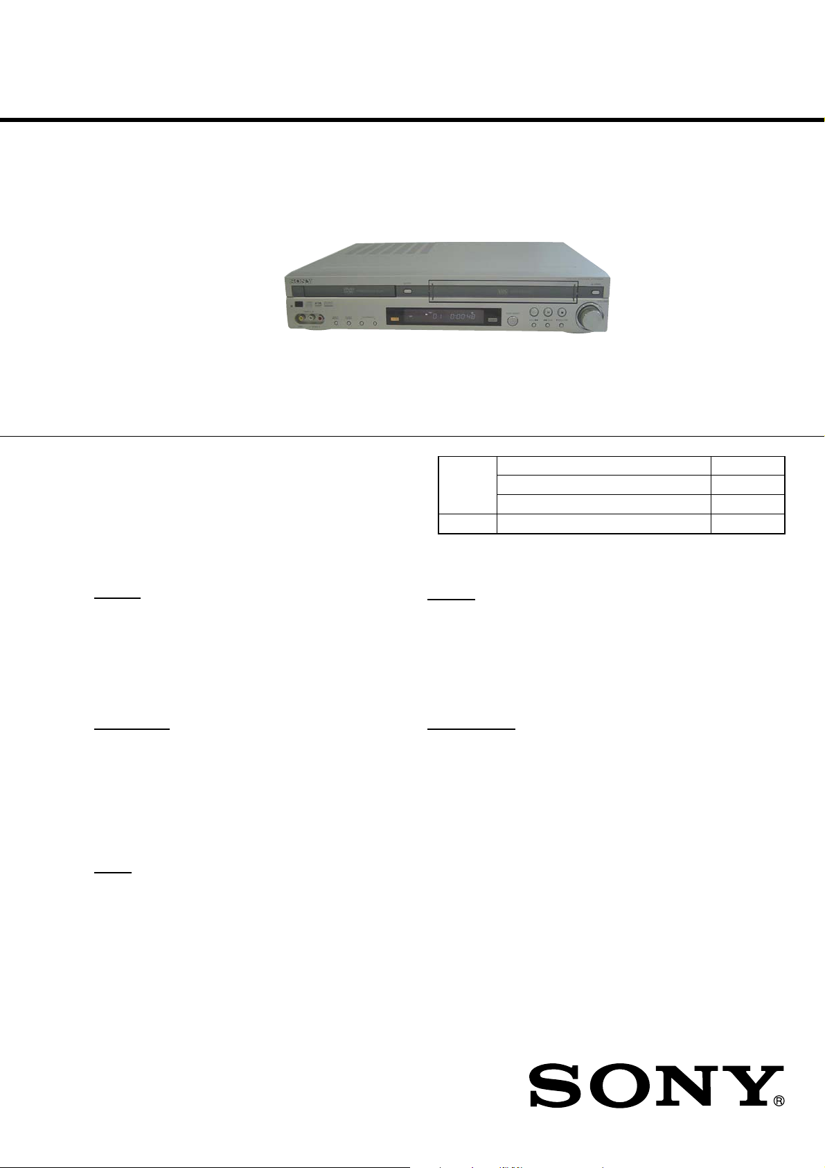
AVD-K700P
SERVICE MANUAL
Ver 1.0 2004.06
AVD-K700P is the amplifier, DVD/VIDEO
player and tuner section in HT-V700DP.
• Manufactured under license from Dolby Laboratories. "Dolb y",
"Pro Logic", and the double-D symbol are trademarks of Dolby
Laboratories.
Confidential unpublished works. Copyright 1992 -1997 Dolby
Laboratories. All rightsreserved.
• DTS and DTS Digital Surround are registered trademarks of
Digital Theater Systems, Inc.
SPECIFICATIONS
General
Power requirements AC 120V, 60 Hz
Power consumption 110 W
Dimensions (approx.) 430 x 83 x 376 mm (17 x 3
Mass (approx.) 6.2 kg (13 lb11 oz)
Operating temperature 5˚C to 35˚C (41˚F to 95˚F)
Operating humidity 5 % to 90 %
Signal system NTSC
DVD Section
Laser system Semiconductor laser (Wavelength
Frequency response DVD (PCM 48 kHz): 8 Hz to 22 kHz,
Signal-to-noise ratio More than 80 dB (AUDIO OUT
Harmonic distortion Less than 0.3%
Dynamic range More than 85 dB (AUDIO OUT
Inputs
ANTENNA IN Antenna or CATV input, 75 ohms
VIDEO IN 1 Vp-p 75 ohms, sync negative,
AUDIO IN -6.0 dBm more than 47 kohms,
FM ANTENNAIN FM antenna input, 75 ohms
AM ANTENNAIN AM antenna input, 300 ohms
OPTICAL IN Optical connector x 1
7
/8inches) (W x H x D)
14
DVD : 650 nm, CD : 780nm)
CD: 8 Hz to 20 kHz
jacks)
jacks)
RCA jack x 2
RCA jack (L, R) x 2
3
/8 x
DVD Mechanism T ype DP-7C
VCR Mechanism T ype D-37
Outputs
COMPONENT VIDEO OUT
Audio output (analog audio) 2.0 Vrms (1 KHz, 0 dB), 330 ohms,
VIDEO Section
Maximum recording time SP: 2 HOURS (T-120), EP: 6 HOURS
US Model
Model Name Using Similar Mechanism AVD-K600P
Optical Pick-up Name PVR-502W
VIDEO OUT 1 Vp-p 75 ohms, sync negative
ANTENNA OUT Channel 3 or 4 (Switchable)
Head system 4 heads helical scan azimuth system
Timer 12-hour display type with AM, PM
Tape speed SP: 33.35 mm/sec, EP: 11.12 mm/sec
Tape width 12.7 mm
Rewind time About 150 seconds (T-120)
Antenna 75 ohms (VHF/UHF)
Channel coverage VHF: 2-13, UHF: 14-69, CATV: 1-125
Frequency range 20Hz to 20kHz
Signal-to-noise ratio More than 43dB
Dynamic range More than 85 dB (AUDIO OUT jacks)
Channel separation More than 55 dB (AUDIO OUT jacks)
(Y) 1.0 V (p-p), 75 ohms, negative
sync, RCA jack x 1
(P
B/CB
)/(PR/CR) 0.7 V (p-p), 75 ohms,
RCA jack x 2
RCA jack (L, R) x 1
(T-120)/8 HOURS (T-160)
(4A, A-W, W+1 - W+84, A-5 - A-1)
– Continued on next page –
9-879-041-01
2004F1678-1
© 2004.06
DVD/VCR RECEIVER
Sony Corporation
Home Audio Company
Published by Sony Engineering Corporation
Page 2
AVD-K700P
FM Tuner
Intermediate Frequency
Tuning Range
87.5 - 108.0 MHz
10.7 MHz
AM Tuner
Intermediate Frequency
Tuning Range
530 - 1,720 kHz
450 kHz
AUDIO POWER SPECIFICATION
POWER OUTPUT AND TOTAL
HARMONIC DISTORTION:
With 6 ohm loads, both channels
driven, from 120 - 20,000 Hz; rated
90 watts per channel minimum RMS
power, with no more than 10 % total
harmonic distortion from 250 milli
watts to rated output (USA model
only).
Amplifier
Stereo mode 90 W + 90 W (6Ω at 1 kHz, THD
Surround mode Front: 90 W/ch (6Ω at 1 kHz, THD
Inputs VIDEO 1, VIDEO 2, OPTICAL IN
Design and specifications are subject to change without notice.
10 %)
10 %)
Center*: 90 W (6Ω at 1 kHz, THD
10 %)
Surround*: 90 W/ch (6Ω at 1 kHz,
THD 10 %)
Subwoofer*: 150 W (4Ω at 30 Hz,
THD 10 %)
*
Depending on the sound mode settings
and the source, there may be no sound
output.
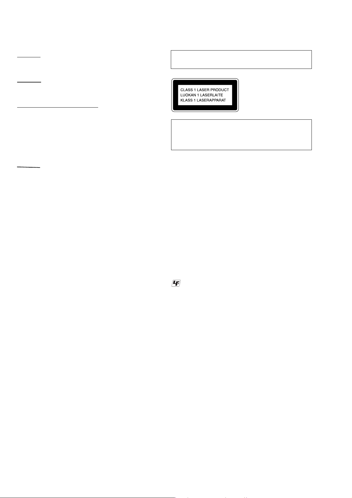
Laser component in this product is capable of emitting radiation
exceeding the limit for Class 1.
This appliance is classified as
a CLASS 1 LASER product.
The CLASS 1 LASER
PRODUCT MARKING is
located on the rear exterior.
CAUTION
Use of controls or adjustments or performance of procedures
other than those specified herein may result in hazardous radiation
exposure.
Notes on chip component replacement
• Never reuse a disconnected chip component.
• Notice that the minus side of a tantalum capacitor may be
damaged by heat.
Flexible Circuit Board Repairing
• Keep the temperature of the soldering iron around 270 °C
during repairing.
• Do not touch the soldering iron on the same conductor of the
circuit board (within 3 times).
• Be careful not to apply force on the conductor when soldering
or unsoldering.
UNLEADED SOLDER
Boards requiring use of unleaded solder are printed with the leadfree mark (LF) indicating the solder contains no lead.
(Caution: Some printed circuit boards may not come printed with
the lead free mark due to their particular size)
SAFETY-RELATED COMPONENT WARNING!!
COMPONENTS IDENTIFIED BY MARK 0 OR DOTTED LINE
WITH MARK 0 ON THE SCHEMATIC DIAGRAMS AND IN
THE PARTS LIST ARE CRITICAL TO SAFE OPERATION.
REPLACE THESE COMPONENTS WITH SONY PARTS WHOSE
PART NUMBERS APPEAR AS SHOWN IN THIS MANUAL OR
IN SUPPLEMENTS PUBLISHED BY SONY.
: LEAD FREE MARK
Unleaded solder has the following characteristics.
• Unleaded solder melts at a temperature about 40 °C higher
than ordinary solder.
Ordinary soldering irons can be used but the iron tip has to be
applied to the solder joint for a slightly longer time.
Soldering irons using a temperature regulator should be set to
about 350 °C.
Caution: The printed pattern (copper foil) may peel away if
the heated tip is applied for too long, so be careful!
• Strong viscosity
Unleaded solder is more viscou-s (sticky, less prone to flow)
than ordinary solder so use caution not to let solder bridges
occur such as on IC pins, etc.
• Usable with ordinary solder
It is best to use only unleaded solder but unleaded solder may
also be added to ordinary solder.
2
Page 3
AVD-K700P
r
SAFETY CHECK-OUT
After correcting the original service problem, perform the following
safety check before releasing the set to the customer:
Check the antenna terminals, metal trim, “metallized” knobs, screws,
and all other exposed metal parts for AC leakage.
Check leakage as described below.
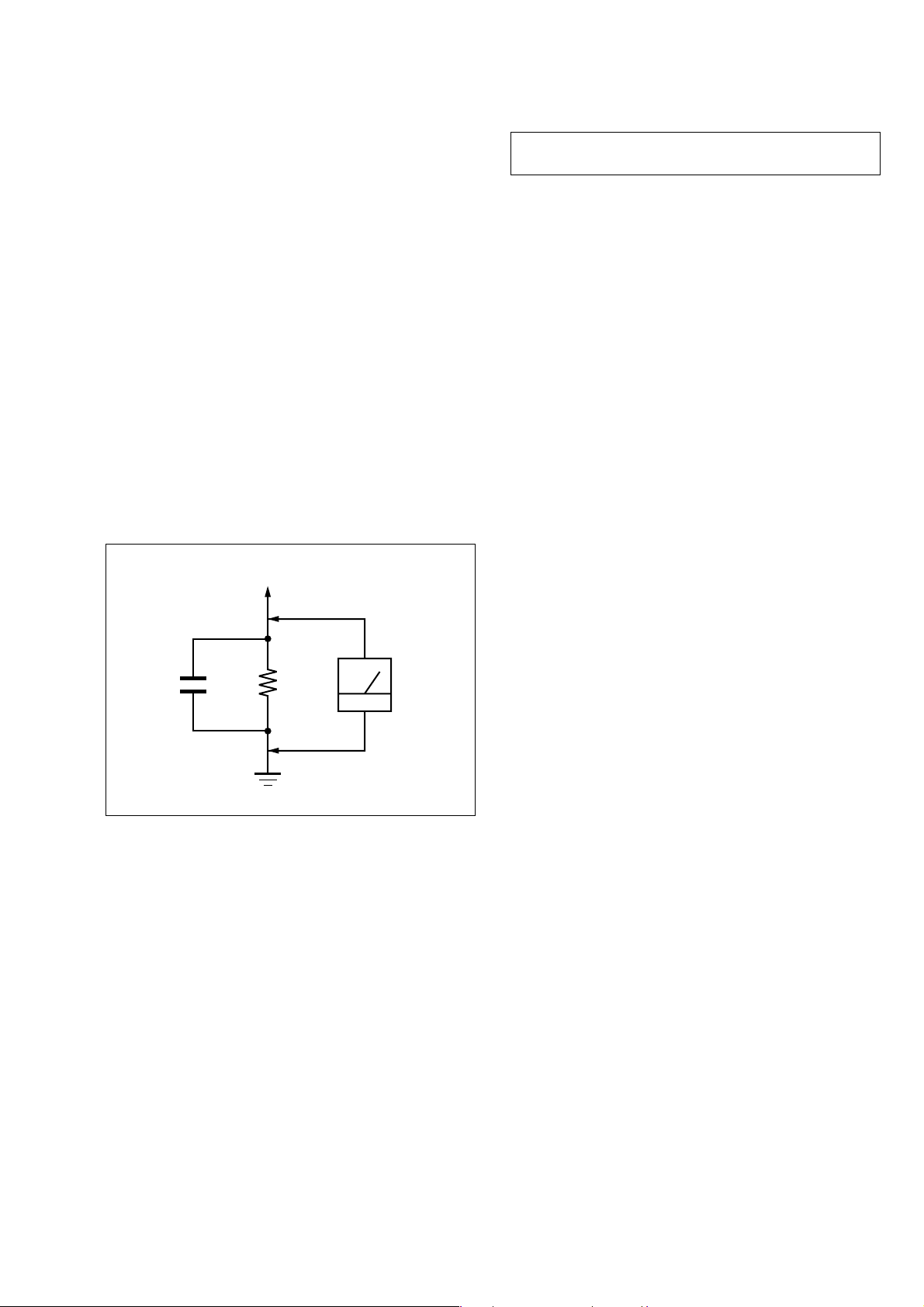
LEAKAGE TEST
The AC leakage from any exposed metal part to earth ground and
from all exposed metal parts to any exposed metal part having a
return to chassis, must not exceed 0.5 mA (500 microamperes.).
Leakage current can be measured by any one of three methods.
1. A commercial leakage tester, such as the Simpson 229 or RCA
WT -540A. Follow the manuf acturers’ instructions to use these
instruments.
2. A battery-operated A C milliammeter . The Data Precision 245
digital multimeter is suitable for this job.
3. Measuring the voltage drop across a resistor by means of a
VOM or battery-operated AC v oltmeter. The “limit” indication
is 0.75 V, so analog meters must have an accurate low-v oltage
scale. The Simpson 250 and Sanwa SH-63Trd are examples
of a passive VOM that is suitable. Nearly all battery operated
digital multimeters that have a 2 V A C range are suitable. (See
Fig. A)
To Exposed Metal
Parts on Set
NOTES ON HANDLING THE OPTICAL PICK-UP
BLOCK OR BASE UNIT
The laser diode in the optical pick-up block may suffer electrostatic
break-down because of the potential difference generated by the
charged electrostatic load, etc. on clothing and the human body.
During repair, pay attention to electrostatic break-down and also
use the procedure in the printed matter which is included in the
repair parts.
The flexible board is easily damaged and should be handled with
care.
NOTES ON LASER DIODE EMISSION CHECK
The laser beam on this model is concentrated so as to be focused on
the disc reflective surface by the objective lens in the optical pickup block. Therefore, when checking the laser diode emission,
observe from more than 30 cm away from the objective lens.
LASER DIODE AND FOCUS SEARCH OPERATION
CHECK
Carry out the “S curve check” in “CD section adjustment” and check
that the S curve waveform is output several times.
AC
0.15 µF
1.5 k
Ω
Earth Ground
voltmete
(0.75 V)
Fig. A. Using an AC voltmeter to check AC leakage.
3
Page 4

AVD-K700P
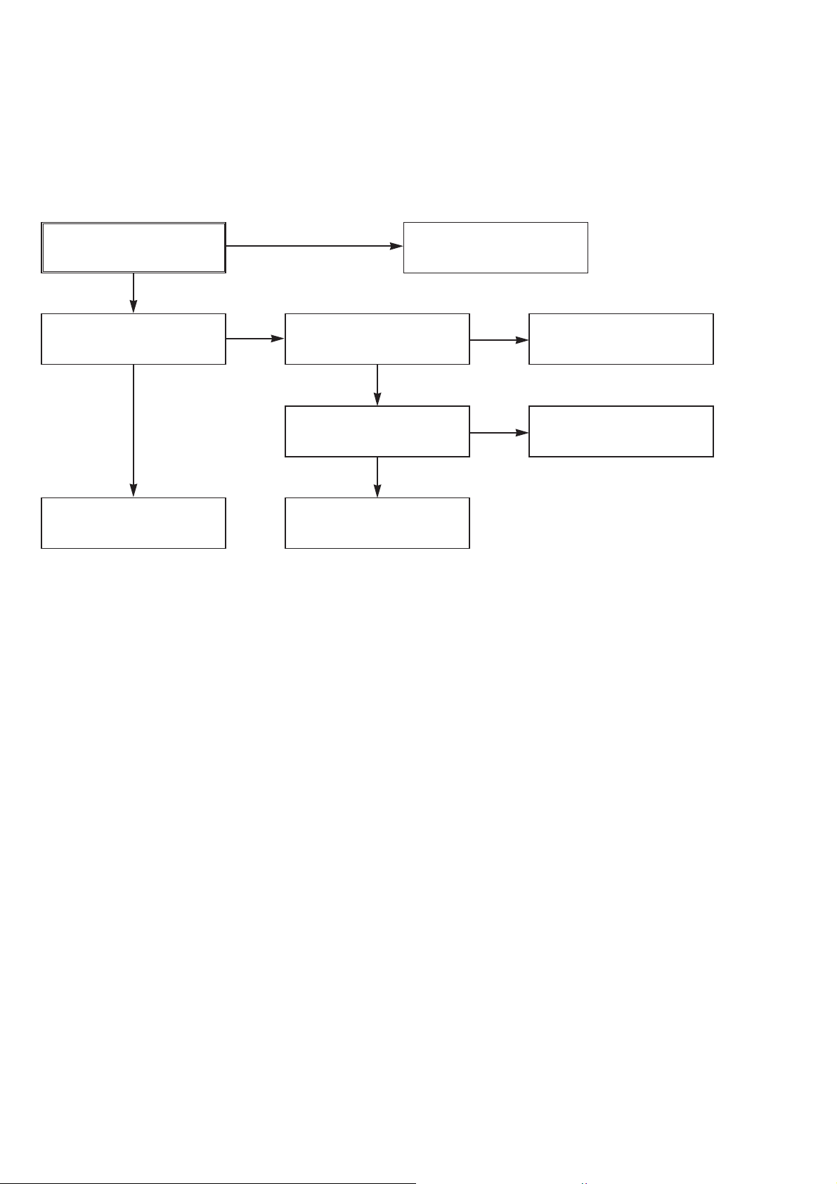
TABLE OF CONTENTS
1. GENERAL ................................................................... 5
2. ELECTRICAL ADJUSTMENT
2-1. VCR Section Electrical Adjustment ................................ 9
2-2. Electrical Troub leshooting Guide.................................... 10
2-3. DVD & AMP Section
Electrical Troubleshooting Guide.................................... 24
3. MECHANICAL ADJUSTMENT
3-1. Video Mechanism Deck Section ..................................... 32
3-2. Maintenance/Inspection Procedure ................................. 39
4. EXPLODED VIEWS
4-1. Block Diagram – POWER (SMPS) Section-1 – ............. 44
4-2. Block Diagram – POWER (SMPS) Section-2 – ............. 45
4-3. Block Diagram – Y/C Section – ...................................... 46
4-4. Block Diagram – NORMAL AUDIO Section –.............. 47
4-5. Block Diagram – HI-FI Section – ................................... 48
4-6. Block Diagram – SYSTEM Section –............................. 49
4-7. Schematic Diagram – POWER Section-1 – ................... 50
4-8. Schematic Diagram – POWER Section-2 – ................... 51
4-9. Schematic Diagram – SYSTEM Section –..................... 52
4-10. Schematic Diagram – AVCP Section – .......................... 53
4-11. Schematic Diagram – HI-FI/TUNER Section –............. 54
4-12. Schematic Diagram – A/V JACK, SCART Section – .... 55
4-13. Schematic Diagram – KEY/TIMER Section –............... 56
4-14. Schematic Diagram – MPEG & VIDEO Section – ........ 57
4-15. Schematic Diagram – RF & SERVO Section –.............. 58
4-16. Schematic Diagram – AUDIO MICOM Section – ......... 59
4-17. Schematic Diagram – DIGITAL AMP Section – ........... 60
4-18. Schematic Diagram – PWM & CODEC Section – ........ 61
4-19. Schematic Diagram – INTERFACE Section – ............... 62
4-20. Printed Wiring Board – VCR Section –........................... 63
4-21. Printed Wiring Board – DISPLAY Section – .................. 64
4-22. Printed W iring Board
– DVD & AMP Section (Component Side) – ................. 65
4-23. Printed W iring Board
– DVD & AMP Section (Conductor Side) – ................... 66
4-24. Printed Wiring Board – SMPS Section – ........................ 67
4-25. Printed Wiring Board – KEY Section – .......................... 68
5. EXPLODED VIEWS
5-1. Overall Section ................................................................ 69
5-2. DVD Mechanism Deck ................................................... 70
5-3. Front Loading Mechanism Section ................................. 71
5-4. Moving Mechanism Section (1)...................................... 72
5-5. Moving Mechanism Section (2)...................................... 73
6. ELECTRICAL PARTS LIST .................................. 74
4
Page 5
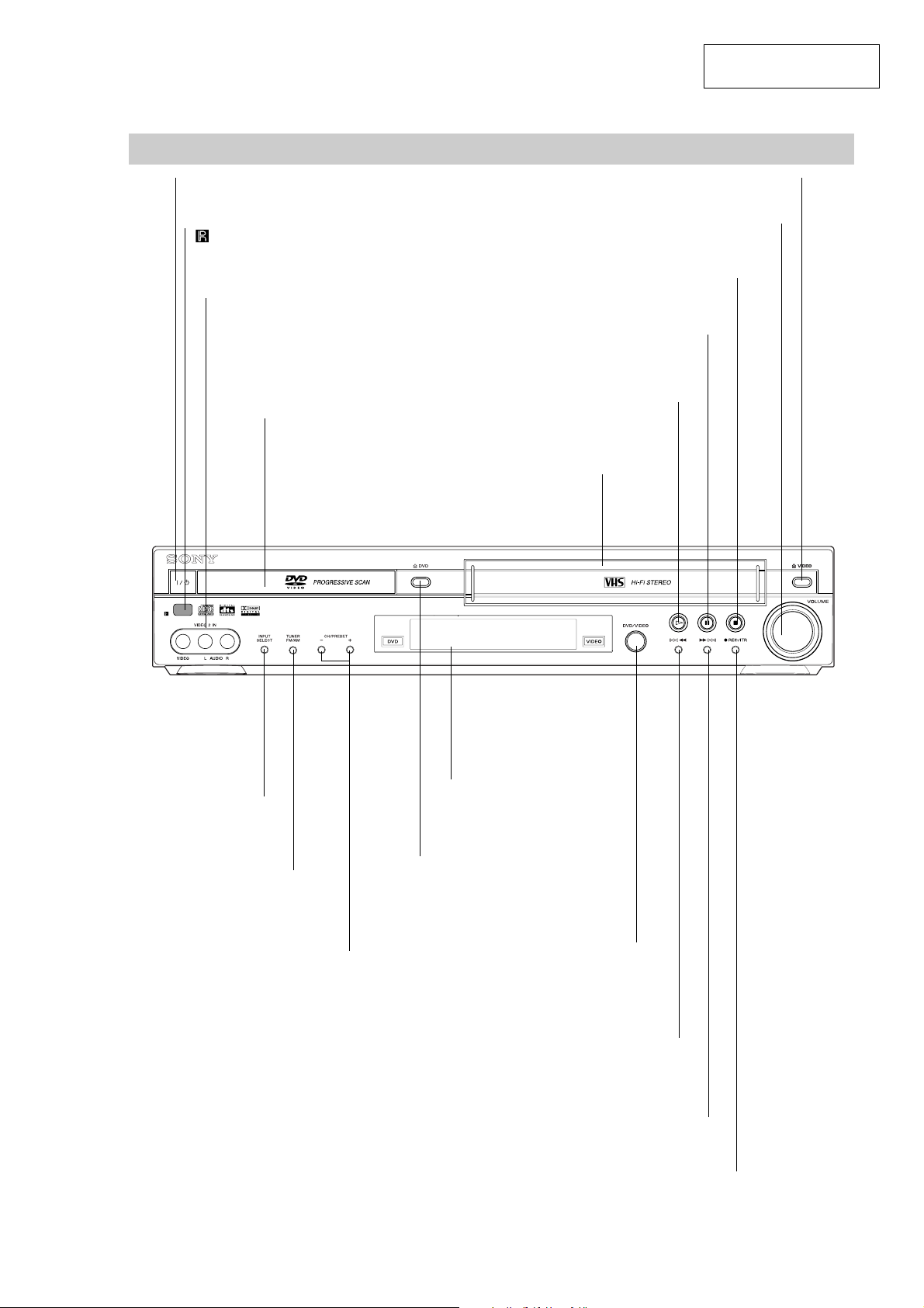
Front Panel
ML
DVD: Go to NEXT chapter/track. Press and hold for a fast forward search.
VIDEO: Advances the tape from STOP mode or for fast forward picture search.
X (PAUSE)
Pause playback or recording
temporarily.
z REC/ITR
To record normally or to activate Instant Timer Recording.
A DVD
Opens or closes
the disc tray.
Remote Sensor
Point the DVD/VCR Receiver remote
control here.
Display window
Shows the current status of the DVD/VCR
Receiver.
Disc Tray (DVD deck)
Insert a disc here.
@ / 1
Switches the DVD/VCR Receiver ON and OFF.
lm
DVD: Go to beginning of current chapter/track or to previous chapter/track.
Press and hold for a fast reverse search.
VIDEO: Rewinds the tape from STOP mode or for fast reverse picture search.
H (PLAY)
To play back a disc or
a recorded tape.
x (STOP)
Stops playback or recording.
INPUT SELECT
Selects the VIDEO
deck’s source
(Tuner, LINE 1 or
LINE 2).
CH/PRESET (+/–)
Scans up or down through
memorized channels or radio
frequencies (stations).
TUNER FM/AM
Selects Radio opera-
tion mode.
VIDEO 2 IN(VIDEO/AUDIO IN (Left/Right))
- Connect the audio/video output of an
external source (Audio system, TV/ Monitor,
another VCR).
- Use the left channel when external source is
MONO.
Video Cassette Compartment (VIDEO deck)
Insert a video cassette here.
A VIDEO
Ejects the tape in the VIDEO deck.
VOLUME
Adjusts sound level of speakers.
DVD/VIDEO
Toggles control
between the DVD deck
and the VIDEO deck.
SECTION 1
GENERAL
AVD-K700P
This section is extracted
from instruction manual.
5
Page 6
AVD-K700P
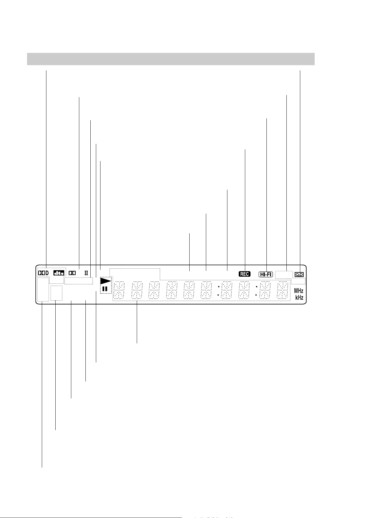
Display Window
Indicates encoding format of the
current disc.
Indicates sound mode is
DOLBY PROLOGIC II.
Indicates repeat mode
Lights when TV mode is
active.
VIDEO DVD/VCR
Receiver is recording.
A cassette is in the VIDEO deck.
SP EP Displays the recording
and playback speed.
HI-FI Indicates the unit is
playing back a tape record-
ed in Hi-Fi.
REC DVD/VCR Receiver
is Recording.
TIMER DVD/VCR Receiver is in
timer recording or a timer recording
is programmed.
TUNED Indicates a AM or FM
broadcast is being received.
ST (STEREO) Indicates a
stereo broadcast is being
received.
PL
PCM
MP3
DVD
VCD
MP3 MP3 disc inserted
DVD DVD inserted.
VCD Video CD inserted
REP 1A - B TV
PROGRESSIVE
PBC
SAP
SHUF PGM
SHUFFLE Random playback active
PBC Indicates PBC On mode
SAP Indicates when a SAP BILINGUAL broadcast
is being received.
VIDEO
PGM Programmed playback active.
TITLE CHAP
Indicates when the Progressive scan playback is in progress.
TRK ST TUNED
Indicates clock, total playing time, elapsed time, chapter number, track
number, channel, radio frequency, volume, channel or current deck
status (Playback, Pause, etc).
TIMER
SP
EP
6
Page 7
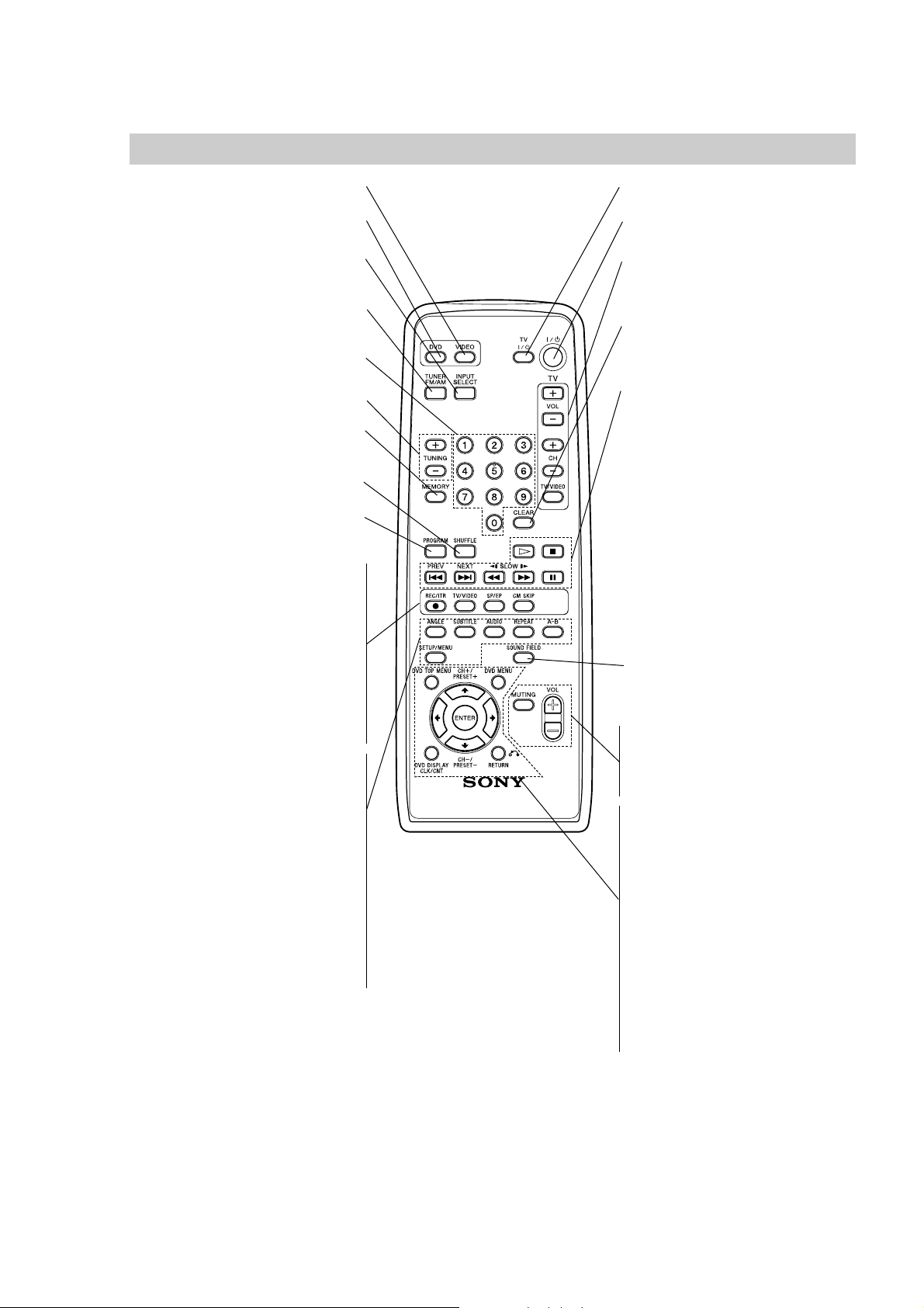
Remote Control
AVD-K700P
VIDEO
Select the output source to VIDEO.
DVD
Sets the output source to DVD.
INPUT SELECT
Selects the VIDEO deck’s source
(L1 OPT, LINE1, LINE2, Tuner).
TUNER FM/AM
Selects the DVD/VCR Receiver’s tuner as
the listening choice. (FM and AM bands)
0-9 numerical buttons
Selects numbered options in a menu.
TUNING (+/–)
To tune in the desired station.
MEMORY
Memorize a radio station frequency into
the tuner.
SHUFFLE
Plays tracks in random order.
PROGRAM
Enters to the program edit mode or exits
from that.
z REC/ITR
Records normally or activates Instant
Timer Recording.
TV/VIDEO
To view channels selected by the VIDEO
tuner or by the TV tuner.
SP/EP
Selects recording speed.
CM SKIP
Fast forwards picture search through 30
seconds of recording.
ANGLE
Selects a DVD camera angle if available.
SUBTITLE
Selects a subtitle language.
AUDIO
Selects an audio language (DVD) or an
audio channel (CD).
REPEAT
Repeat chapter, track, title, all.
A-B
Repeats sequence.
SETUP/MENU
Accesses or returns DVD setup menu
and VIDEO setup menu.
TV @ / 1
Switches TV ON and OFF.
@ / 1
Switches DVD/VCR Receiver ON and OFF.
TV Control Buttons (see page 40)
• VOL +/–: Adjusts TV’s volume.
• CH +/–: Selects TV’s channel.
• TV/VIDEO: Selects the TV’s source.
CLEAR
Removes a track number on the program
menu. To clear preset stations from the
tuner memory.
Playback Control Buttons
• H (PLAY)
Starts playback.
• x (STOP)
Stops playback.
• . (PREV) (DVD mode only)
Go to beginning of current chapter or
track or go to previous chapter or track.
• > (NEXT) (DVD mode only)
Go to next chapter or track.
• m/M (SLOW t/T)
DVD: For picture search or slow playback backward or forward.
VIDEO: Rewinds or advances the tape
in STOP mode or for picture search.
• X (PAUSE)
Pause playback or recording temporarily.
SOUND FIELD
Selects sound mode between AUTO,
PRO LOGIC, PRO LOGIC II (MOVIE,
MUSIC, MATRIX) and 3D SURROUND.
VOL (+/-)
Adjusts speaker volume.
MUTING
Momentarily silence the speaker of the
DVD/VCR Receiver.
DVD TOP MENU
Displays the disc’s Title menu, if available.
DVD MENU
Accesses menu on a DVD disc.
B/b/V/v (left/right/up/down)
Selects an option in the menu.
CH/PRESET(+/–): Selects a program of
VIDEO or Tuner. Adjusts manually the
tape’s picture onscreen.
ENTER
Acknowledges menu selection.
DVD DISPLAY, CLK/CNT
Accesses On-Screen display. Switches
among the clock and tape counter.
RETURN
Returns the setup menu.
Note
This remote control uses the same buttons for VIDEO and DVD
functions (ex. PLAY).
To use the VIDEO, first press the VIDEO button.
To use the DVD, first press the DVD button.
7
Page 8
AVD-K700P
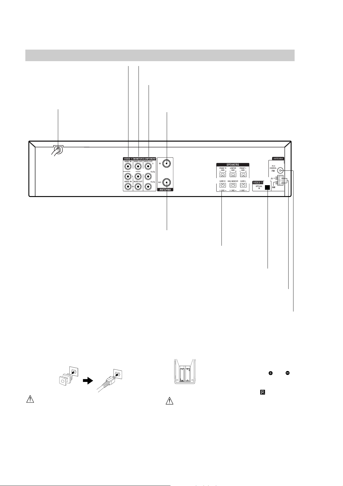
Rear Panel
VIDEO 1 (VIDEO/AUDIO IN (Left/Right))
Connect the audio/video output of an
external source (Audio system, TV/Monitor,
Another VCR).
AC Power Cord
Plug into the power
source.
ANTENNA OUT (DVD/VIDEO OUT)
Connect to a TV with RF coaxial inputs.
Connect the six supplied speakers to these terminals.
MONITOR (VIDEO / AUDIO OUT (Left/Right))
Connect to a TV with video and audio inputs.
COMPONENT VIDEO OUT (Y P
B/CBPR/CR
(DVD OUT)
Connect to a TV with Y P
B/CBPR/CR
inputs. FOR DVD
VIEWING ONLY.
ANTENNA IN
Connect the VHF/UHF/CATV
antenna to this terminal.
SPEAKERS Connectors
)
Connect to a digital audio output on a digital device.
Dust Protection Cap
Remove the dust protection cap from the OPTICAL IN
jack and connect the optical digital cable (not supplied)
securely so that the configurations of both the cable
and the connector match. Keep the dust protection cap
and always reattach the cap when not using the connector to protect against dust intrusion.
Do not touch the inner pins of the jacks on the rear
panel. Electrostatic discharge may cause permanent
damage to the unit.
OPTICAL IN
AM ANTENNA Connectors
Connect the AM antenna to this terminal.
FM ANTENNA Connectors
Connect the FM antenna to this terminal.
Remote control battery installation
Detach the battery cover on the rear
of the remote control, and insert two
AA
AA
Caution
Do not mix old and new batteries. Never mix different
types of batteries (standard, alkaline, etc.).
R6 (size AA) batteries with and
aligned correctly.
When using the remote control, point
it at the remote sensor on the unit.
8
Page 9
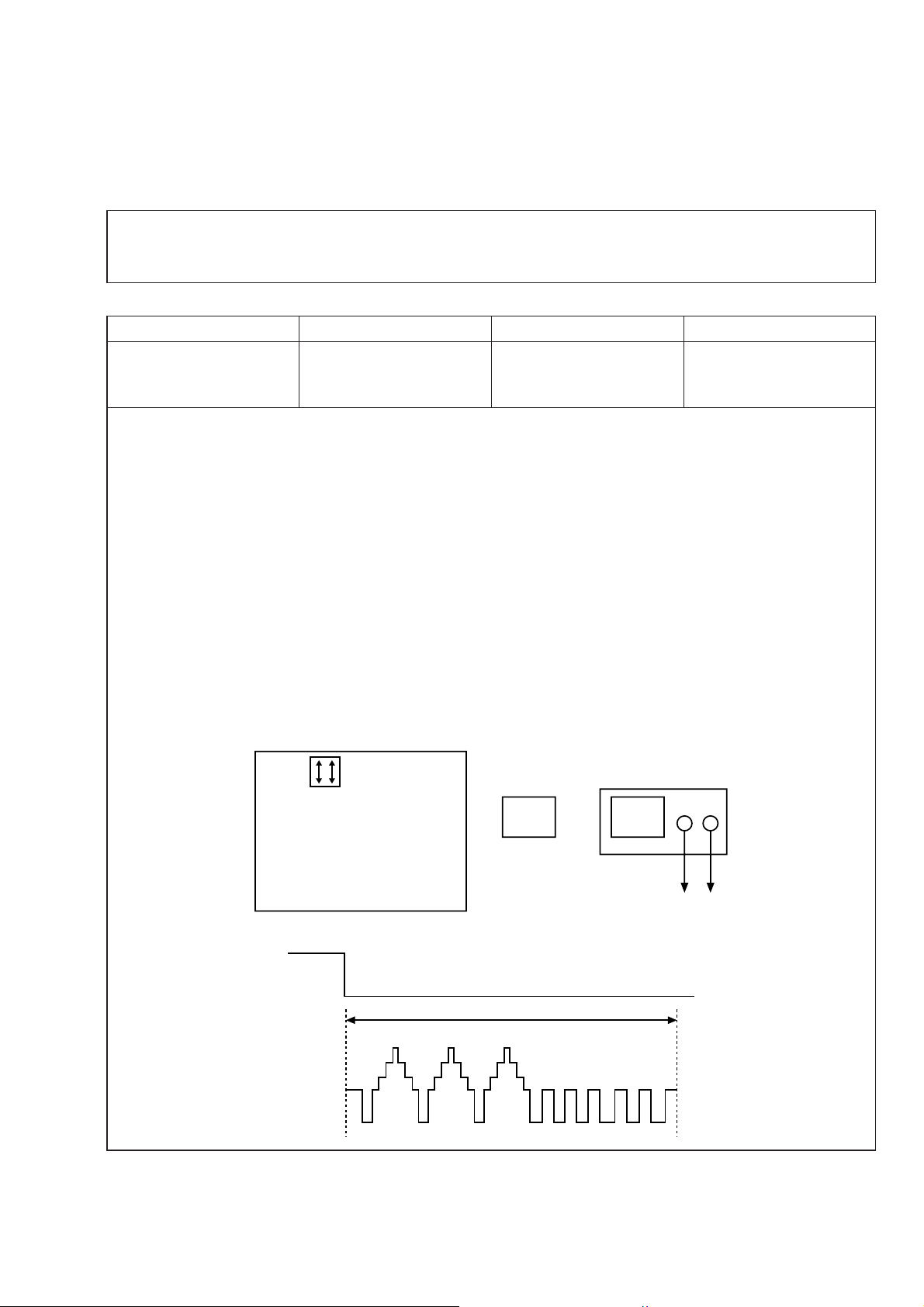
SECTION 2
ELECTRICAL ADJUSTMENT
2-1. VCR SECTION ELECTRICAL ADJUSTMENT
1. Servo Adjustment
1) PG Adjustment
• Test Equipment
a) OSCILLOSCOPE
b) NTSC MODEL : NTSC SP TEST TAPE
• Adjustment And Specification
AVD-K700P
MODE
PLAY
MEASUREMENT POINT ADJUSTMENT POINT SPECIFICATION
V.Out
H/SW(W373, W374)
R/C TRK JIG KEY 6.5 ± 0.5H
• Adjustment Procedure
a) Insert the SP Test Tape and play.
b) Press the “O” key on the Remote controller and the “PLAY” key on the Front Panel the same time, the
unit then goes in to Tracking initial mode.
c) Trigger the mixed Combo Video Signal of CH2 to the CH1 H/SW(W373, W374), and then check the dis-
tance (time difference), which is from the selected A(B) Head point of the H/SW(W373, W374) signal to
the starting point of the vertical synchronized signal, to 6.5H ± 0.5H (412µs, 1H=63µs).
Note - Press FRONT CH UP KEY and FRONT PLAYKEYon Deck playback, and it goes in to ATR PRE-
SET. after the SP Test Tape is inserted.
• PG Adjustment Method
a-1) Playback the SP standard tape
b-2) Press the “O” key on the Remote controller and the “PLAY” key on the Front Panel the same time,
Tracking initial mode.
c-3) Repeat the above step(No.b-2), the unit will then finish the PG adjusting automatically.
d-4) Stop the playback, the unit then exits PG adjusting mode after saving the PG data.
• CONNECTION
V.Out
•WAVEFORM
H/SW(W373, W374)
H/SW
Composite
VIDEO
6.5H(412µs)
R/C KEY
OSCILLOSCOPE
CH1 CH2
H/SW
(W373, W374)
V.out
9
Page 10
AVD-K700P
2-2. ELECTRICAL TROUBLESHOOTING GUIDE
1. Power(SMPS) CIRCUIT
(1) No 5.3VA (SYS/Hi-Fi/TUNER)
NO 5.3VA.
YES
Is the F101 normal?
YES
Is the BD101
NO
NO
Replace the F101.
(Use the same Fuse)
normal?
YES
Is the TH101
normal?
YES
Is Vcc(8.5~21V) sup-
NO
NO
Replace the TH101.
plied to IC104 Pin3?
YES
Check or Replace
the D105.
Replace the
BD101.
Is the D105
normal?
NO
(2) No 12VA (TO CAP, DRUM MOTOR)
NO 12VA.
YES
Is the Vcc(13V) supplied
NO
to (+) terminal in D126?
YES
Check or Replace
the D126.
Check or Replace
the Motor Vcc.
(3) No 5.0V (SYS/Hi-Fi/TUNER)
Is the D129
normal?
YES
Is there about 2.5V
at the IC106 Vref?
YES
Check the Main PCB
5.3VA/5.0V Line short?
NO
NO
Replace the D129.
Replace the IC106.
NO 5.0VA.
YES
Is 5.3VA put into
the Q167 Emitter?
YES
Is the Q169 Base
“H”?
YES
Is about 5V put into
the Q167 Base?
YES
Check or Replace
the Q167/Q169.
NO
NO
NO
5.3VA Line Check.
Check the Power
Control.
Check or Replace the
Q169, R175, R176, R177.
10
Page 11
AVD-K700P
(4) No 5V (TO DVD)
NO 5V.
YES
Is 5.3VA put into
the Q168 Emitter?
YES
Is the Q169 Base
“H”?
YES
Is about 5V put into
the Q168 Base?
YES
Check or Replace
the Q168/Q169
NO
NO
NO
5.3VA Line Check.
Check the Power
Control.
Check or Replace the
Q169, R175, R176, R177.
(5) No 33V (TUNER)
No 33V.
YES
Is Q163 Base “H”?
YES
Check or Replace
Q163, R168, R169.
NO
Check the Power
Control.
(6) No 8V(TO DVD)
NO 8V.
YES
Is Vcc(13V) supplied to
(+) terminal in D126?
YES
Is Vcc(12V) supplied
to IC160 Pin1?
YES
Check or Replace
IC161, C163.
NO
NO
Check or Replace
the D126.
Check or Replace
the D163.
11
Page 12
AVD-K700P
2. SYSTEM/KEY CIRCUIT
(1) AUTO STOP
Auto Stop
YES
Does the SW30 waveform
appear at the IC501
Pin18?
YES
Do the T-UP Reel Pulses
appear at the IC501 Pin80?
YES
Replace the IC501.
NO
NO NO
Check the Drum Motor
signal.
Do T/UP Reel Pulses
appear at the point
between R556 and R536?
YES YES
Replace the T/UP Reel
Sensor (RS501).
(2) The unstable loading of a Cassette tape
The unstable loading of a
Cassette tape
YES
Does 5V appear at the
RS501?
NO
Check the Q160 Power
Circuit.
Is 12V applied to the
PMC01 Pin8?
YES
Does the “H” signal appear
at the IC501 Pin58 during
inserting the CST ?
YES
Does the “L” signal appear
at the IC501 Pin60 during
inserting the CST?
YES
Check the Deck
Mechanism.
Caution :
Auto stop can occur because Grease or Oil has dried up
NO
NO
NO
Check the CST SW and
the peripheral circuitry.
Refer to “SMPS DRUM
12 Volt Trouble Shooting”.
Is 5V applied to the
R531 ?
YES
Refer to SMPS 5.3VA
troubleshooting.
Check the IC501
Pins22, 23, 24, 25.
NO
12
Page 13
3. SERVO CIRCUIT
(1) Unstable Video in PB MODE
Unstable Video in
PB Mode.
YES
Does the Noise level of the
screen change
periodically?
YES
AVD-K700P
Do the CTL pulses appear
at the IC501 Pin97?
YES
Does the CFG waveform
appear at the IC501
Pin87?
YES
On tracking do the CTL
pulses move?
YES
Does the Video Envelope
waveform appear at the
IC501 Pin9?
YES
Replace the IC501.
(2) When the Drum Motor
(2) doesn’t run.
When the Drum Motor
doesn’t run,
Does 12V appear at the
PMC01 Pin8?
NO
NO
NO
NO
Is adjusting the height of
the CTL Head accurate?
Replace the IC501.
Refer to “When the Y signal
doesn’t appear on the
screen in PB Mode”.
Refer to “(2)
No 12VA of Power section”
Do the Drum PWM Pulses
appear at the IC501
Pin76?
YES
Aren’t the foil patterns and
the Components between
IC501 Pin76 and PMC01
Pin12 short?
NO
Readjust the height of the
CTL Head.
NO
Do the DFG Pulses appear
at the PMC01 Pin11?
YES
NO
Replace the Cap M.
YES
Does 2.8V appear at the
PMC01 Pin12?
YES
Check the connector
(PMC01) and the Drum
Motor Ass’y .
NO
Do the DFG Pulses appear
at the IC501 Pin90?
YES
Do the Drum PWM Pulses
appear at the IC501
Pin76?
YES
Aren’t the connecting patterns and the Components
between IC501 Pin76 and PMC01 Pin12 short?
NO
NO
Aren’t the foil patterns and
the Components between
IC501 Pin 90 and PMC01
Pin11 short?
Replace the IC501.
13
Page 14
AVD-K700P
(3) When the Capstan Motor doesn’t run,
When the Capstan Motor doesn’t run,
Does 12VA appear at the PMC01?
YES
Is “DRUM CTL” 2.8V appear at the
PMC01?
YES
Check the PMC01 and the Capstan
Motor Ass’y .
Aren’t the foil patterns and Components
between IC501 Pin77 and PMC01
Pin9 short?
Does the CFG signal come into the
IC501 Pin87?
NO
NO
YES
YES
Refer to “SMPS(CAPSTAN/12Volt)
Trouble Shooting”.
Does the PWM signal appear at the
IC501 Pin77?
NO
Does the CFG signal appear at the
PMC01 Pin1?
NO
Check the Capstan Motor Ass’y.
YES
Does the Capstan PWM signal appear at
the IC501 Pin77?
YES
Aren’t the foil patterns and Components
between IC501 Pin77 and PMC01
Pin9 short?
NO
Aren’t the foil patterns and component
between IC501 Pin87 and PMC01
Pin1 short?
NO
Replace the IC501.
14
Page 15
(4) KEY doesn’t working
KEY doesn’t working.
AVD-K700P
Is 5V applied to the IC501
Pin2, 3?
YES
Does LED or FLD change
when a function button is
pressed?
4. OSD CIRCUIT
(1) No OSD display.
No OSD or F.OSD display.
Is 5.3V applied to the
IC501 Pin53?
YES
Does oscillation occur at
the IC501 Pins44, 45?
YES
NO
NO
NO
NO
Refer to “SMPS 5.3VA
Trouble Shooting”.
Replace the defective
switches.
Refer to “SMPS 5.3VA
Trouble Shooting”.
Check or Replace the pheripheral Circurity.(L511,
R598, C596, C595)
Replace the IC501.
2
C BUS CHECK
(2) I
The I2C waves don’t
come out.
Does Power appear at the
Pull up impedence
(R569, R507)?
YES
Replace the IC501.
NO
Refer to “SMPS 5.3VA
Trouble Shooting”.
15
Page 16
AVD-K700P
5. Y/C CIRCUIT
(1) No Video in EE Mode,
No Video in EE Mode
Does the Video signal
appear at the IC301
Pins28, 30, 32?
YES
Is REG 5.0V applied to the
IC301Pins23, 44, 45, 52, 68,
77?
YES
Does the Video signal
appear at the IC301 Pin26?
NO
NO
NO
Does the Video signal
appear at the IC302
Pins1, 5?
YES
Is there 5V at the IC302
Pin6?
YES
Replace the IC302.
Check the REG 5V Line.
(Power Circuit)
Is I2C BUS signal applied to
the IC301 Pins53, 54, 55?
NO
NO
Check DVD Video Input
(IC602, Pin4), Tuner Video
Input (TU701 Pin16), Line
Video Input (JK601),
respectively.
Check the System Circuit.
(Refer to ‘SYSTEM I
CHECK Trouble Shooting’)
2
C BUS
YES
Does the Video signal
appear at the IC501 Pin52?
YES
Does the Video signal
appear at the IC602 Pin7?
NO
NO
YES
Check the path of the signal between the IC301 Pin
26 and IC501 Pins50, 52.
Is there 5V on the plus
terminal of the C614?
YES
Replace the IC602.
NO
Replace the IC301.
Check the REG 5V Line.
(Power Circuit)
16
Page 17
AVD-K700P
(2) When the Y(Luminance) signal doesn’t appear on the screen in PB Mode,
Is 5V applied to the IC301
Pins23, 44, 45, 52, 68, 77?
Is the Y/C Bus siganl
applied to the IC301
Pins53, 54, 55?
Does the normal RF signal
appear at the IC301 Pin14?
Check the line of the REG
5V Line. (Power Circuit)
Check the System Circuit.
(IC501 Pin18)
Check the V.H.S/W level.
Refer to ‘SYSTEM Y/C
BUS CHECK Trouble
Shooting’.
Is the V.H.S/W signal
applied to the IC301 Pin57?
Does the Rectangular
waveform(5V) appear at
the IC301 Pin57(V.H.S/W)
Clean the Drum.
Check the C324.
Check the R328, R347,
C322, C323.
Does the Y(Luminance)
signal appear at the IC301
Pin20?
Is the Y(Luminance) Video
waveform showed up at the
IC301 Pin22?
Replace the IC301.
NO
YES
YES
YES
YES
YES
YES
YES
NO
NO
NO
NO
NO
NO
17
Page 18
AVD-K700P
(3) When the C(Color) signal doesn’t appear on the screen in PB Mode,
Is 5V applied to the IC301
Pins23, 44, 45, 52, 68, 77?
YES
Does the fsc signal appear
at the IC301 Pins41, 50?
YES
Replace the IC301.
NO
NO
Check the line of the REG
5V Line. (Power Circuit)
Is normal the X301
(3.58MHZ) of oscillation
Frequency?
Does the Color signal
appear at the IC301 Pin48?
YES
Replace the IC301.
NO
NO
Replace the X301.
Check the C342, C341,
R333.
18
Page 19
(4) When the Video signal doesn’t appear on the screen in REC Mode,
YES
YES
YES
YES
YES
YES
NO
NO
YES
YES
YES
YES
YES
Check system part
(V.H/SW)
Replace the IC301.
Check the drum
*OPTION
Pins72, 73, 74(SP)
Pins65, 66, 67(EP)
REC mode
Check the EE mode
NO
Is EE mode normal?
Is color
normal?
A
A
YES YES
Is brightness normal?
Does signal appear at
IC301 Pins41, 50?
NO
Check X301 oscillation
frequency.
YES
Is the brightness signal supplied to IC301 Pins18?
Is 5V supplied to IC301
Pins23, 44, 45, 68, 77?
Check the power of Pins23,
44, 45, 52, 68, 77.
Check the 5V power
NO
NO
NO
NO
NO
Is Y/C Bus applied to
IC301 Pins53, 54, 55?
Check the REG 5V power
Check system part
Do X301 and X-TAL
oscillate?
Check X301.
Is V.H SW supplied to
IC301 Pin57?
Does the FM signal appear
at IC301 Pins73(SP)/
66(EP)?
AVD-K700P
19
Page 20
AVD-K700P
6. Tuner/IF CIRCUIT
(1) No Picture on the TV screen
No picture on the TV
screen
YES
Does the Video signal at
the TU701 Pin16.
YES
NO
Is +33V applied to TU701
Pin14?
YES
Is +5V applied to TU701
Pin3?
YES
Does the Clock signal
appear at TU701 Pin9?
YES
Does the data signal
appear at TU701 Pin10?
YES
Replace Tuner.
NO
NO
NO
NO
Check 33V line.
Check 5V line.
Check the lIC Clock Signal
of µ-COM Pin71.
Check the lIC Data Signal
of µ-COM Pin72.
Does the video signal
appear at IC302 Pin7.
YES
Does the Video signal at
the IC501 Pin 52.
YES
Does the Video signal at
the IC602 Pin 7.
YES
Check the signal flow from IC602
Pin7 to JK601 Pin Video out.
NO
NO
NO
Check the signal flow from
IC501 Pin27.(Pin27 is ‘L’
state in Tuner Mode)
Check the signal from IC301
Pin26 to IC501 Pin50.
Check the signal from IC501 Pin52 to IC602 Pin1 and IC602 Pin2.
(IC602 Pin2 is ‘L’state in VHS mode)
20
Page 21
AVD-K700P
(2) No Sound
No Sound.
Check the Vcc of TU701 Pins3, 14.
YES
Check 5.2V, 33V Line.
NO
Check the Tuner SiF signal at IC801
Pin57.
YES
Check the Audio of IC801 Pins78, 80.
YES
Check the Signal flow from IC801 Pins78,
80 to JK601 Audio out(L), (R)
YES
Check the Tuner SIF of TU701 Pin13.
NO
1. Check the Vcc(5.3VA, 9V) of IC801
Pins3, 5, 36, 54.
2. Check the IIC Clock and Data at IC801
Pins37, 38.
NO
21
Page 22
AVD-K700P
7. Hi-Fi Circuit
A.
Hi-Fi Playback.
No sound
Check the Hi-Fi Selection
Switch and the Tape quality.
YES
Is the RF waveform at
IC801 Pin 23 over 3V
Vp-p?
YES
NO
Is Pin 30 of IC801 over
3.5V ?
YES
Check the Vcc of IC801.
(Pins 3, 15, 32, 46)
YES
NO
YES
Is the Head switching signal
IC801 Pin 39 O.K?
YES
NO
NO
Check power.
Check REC start “H” signal
of µ-COM.
Check IC501 Pin 19.
(Audio Swich 30)
Check IC801 Pin 37(Data),
Pin 38(Clock).
YES
Is IC801 Pin 49(A.Mute)
“High”?
YES
Do Audio signals appear at
IC801 Pin 80(L-CH),
78 (R-CH)?
YES
Check the Contact point
of Audio Output.
Check the connection at
P3D01 if good then
Replace IC801.
NO
Check Ports of µ-COM.
Check A.MUTE port of
µ-COM (Pin High of
IC501).
NO
Replace IC801.
22
Page 23
B.
Hi-Fi REC.
It is impossible to record and playback
Hi-Fi Audio signal.
YES
Check Vcc of IC801. (Pins 3, 15, 32, 46)
AVD-K700P
YES
Check IC801 Pin 37(Data),Pin 38(CLOCK).
YES
Is IC501 Pin 84(A.Mute) “High”?
YES
Are Audio signals present at IC801
Pins 78, 80?
YES
Do FM Audio signals appear at IC801
Pin 26?
YES
Is IC801 Pin 17(REC “H”) “High”?
NO
Check Power.
NO
Check ports of µ-COM.
NO
Check the Port of µ-COM.
NO
Check Audio Input signal Line
(9, 11, 12, 71, 73, 74), Tuner(57).
NO
Replace IC801.
YES
Check the Contact Points of Drum
Connector if good then Replace the Drum.
NO
Check the Port of u-COM.
23
Page 24
AVD-K700P
2-3. DVD & AMP SECTION ELECTRICAL TROUBLESHOOTING GUIDE
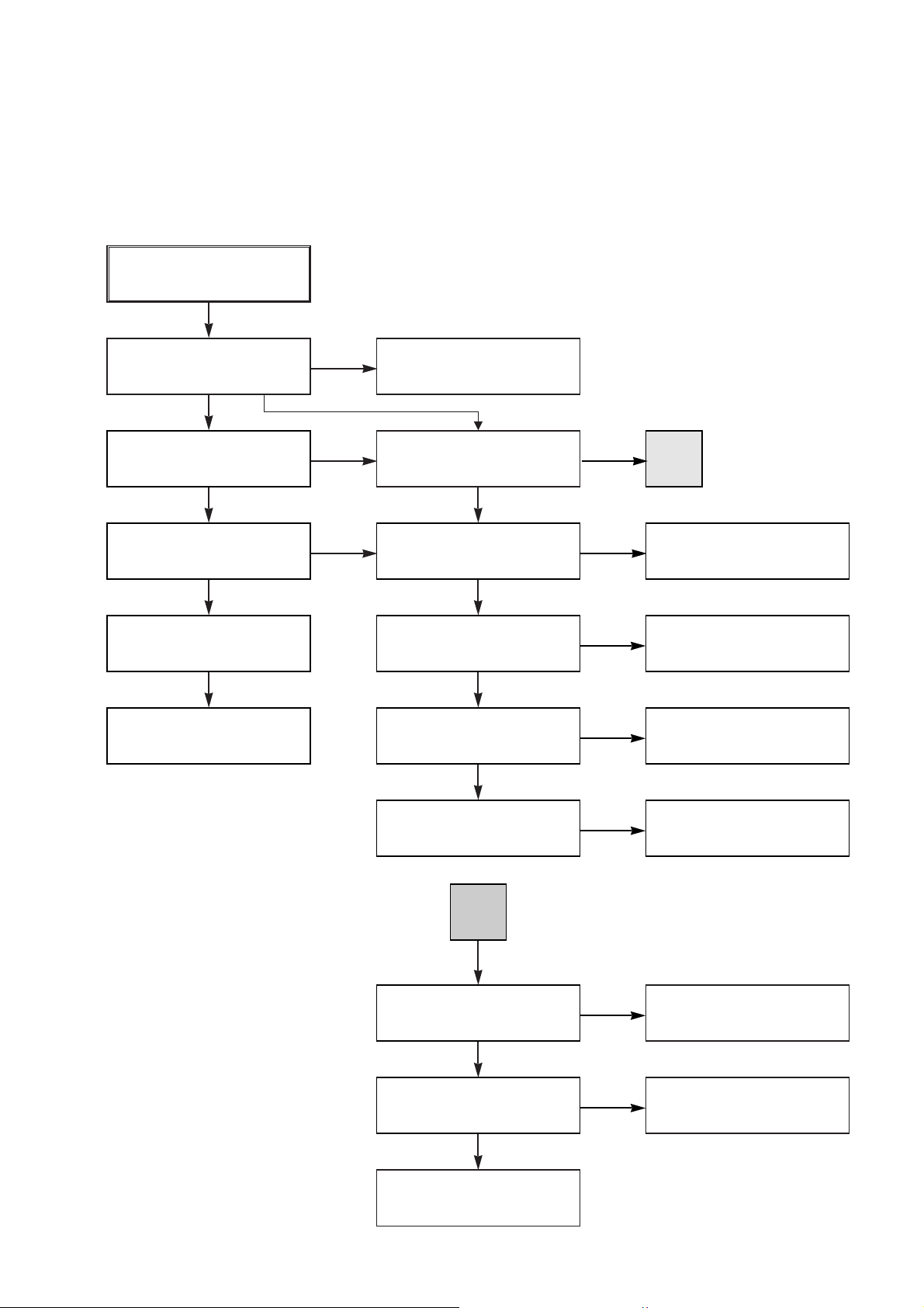
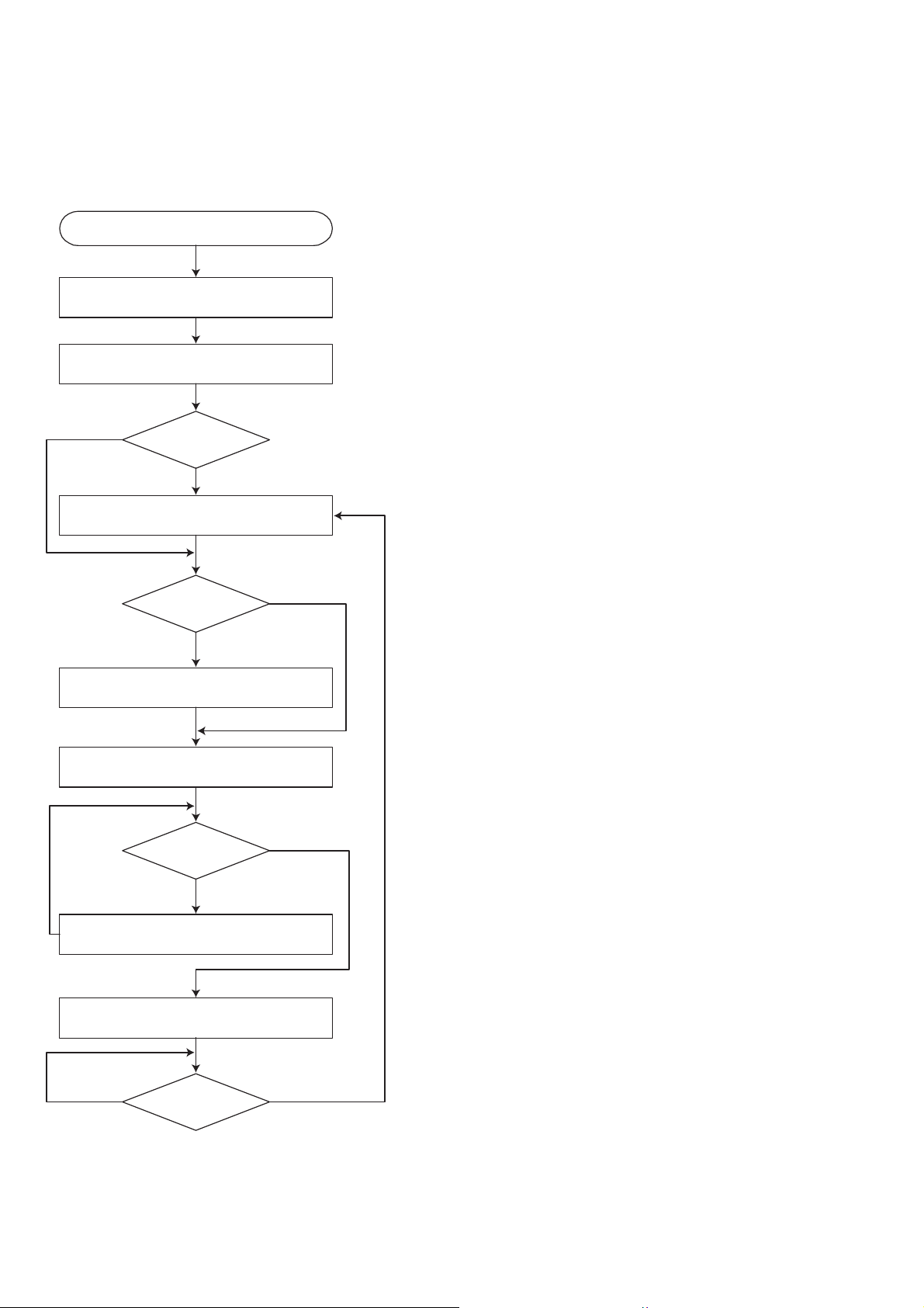
1. System operation flow
Power On
1. 8032 initializes SERVO, DSP & RISC registers
2. Write RISC code to SDRAM
3. Reset RISC
Show LOGO
Yes
SLED Moves to Inner Position
1. Judge whether have disc and disc type
2. Jump to related disc reading procedure
Tray Closed?
No
Tray Close to Closed position
SLED at Inner
Side?
No
Recieve
OPEN/ CLOSE
Key?
Yes
No
1. Execute Pressed Key & IR Key
2. Systemoperati on Routi ne Loop
1. Stop Playback & Open Tray
2. Display tray open message & LOGO
No
Receive
CLOSE Key?
24
Yes
Page 25

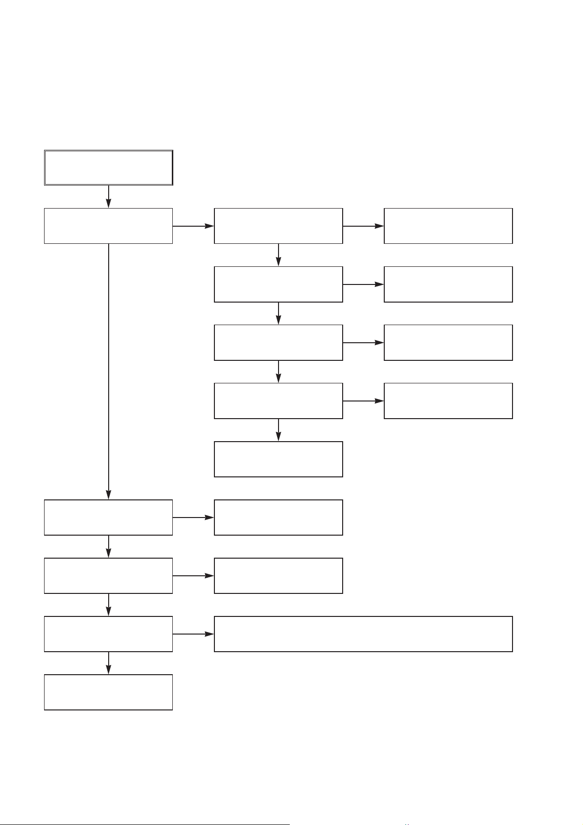
2. Test & debug flow
TEST
AVD-K700P
Check the
AC Voltage
Power PCBA (110V
or 220V)
Yes
Switch on the Power PCBA
Is
the DC Voltage
outputs OK?
(5V, 3.3V, 8V, 12V)
Yes
Is 3.3V and 2.5V DC
outputs normal on main
PCBA?
Yes
Communication between
VCR & DVD is normally?
Yes
No
No
No
No
Check the POWER PART
Check the POWER PART
Check the regulators or diode(D501).
Check the cable connection.
(PDV03)
Connect to PC RS232 Cable and
update the FLASH memory code.
Update
FLASH(IC5A1)
successfully?
Yes
A
No
1. Check 27MHz system clock.
2. Check systemreset circuit.
3. Check FLASH R/Wenable signal PRD,
RWR.
4. Check RS232 SIGNALS.
5. Check FLASH Memory related circuit.
Replace FLASH( IC5A1)
25
Page 26

AVD-K700P
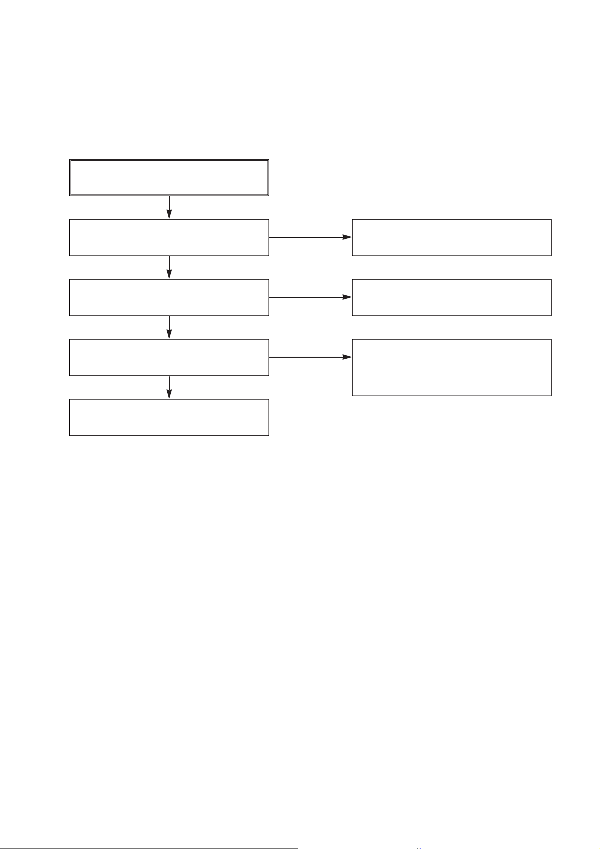
A
RESET or Power On.
Show LOGO?
YES
NO NO
Flash
Memory operates
properly?
YES
SDRAM
works properly?
NO
YES
MT1379
VIDEO outputs
properly?
NO
YES
Have
TV signal output?
NO
YES
Check AV cable
connection to TV set .
Check connection lines between FLASH
& MT1379 and the FLASH access time
whether is sui table or not.
Check connection lines between
SDRAM(IC502,IC503) & MT1379 and the
SDRAM is damaged.
Check the related circuit of MT1379.
(IC501 PIN 161,166, 168 check)
Check the filtering and amp circuit of
TV signal .(IC507)
Does
Tray move inside
when it is not at
closed position?
YES
B
NO
Normal
TROUT & TRIN
signals?
YES
Normal
TRCLOSE &
TROPEN signal?
YES
Normal
LOAD+ & LOAD-
signal ?
YES
Check the cable connection between
main PCBA and loader. (MECHA)
NO
NO
NO
Check the load OPEN &
CLOSE switch
Check the Tray control IO pins
on MT1376 & MT1379.
Check the Tray control amplifying
circuit on Motor driver.(IC402)
26
Page 27

B
Does
the SLED move
to inner side when it is at
outer position?
No
Motor Driver STBY
Pin is High?
No
AVD-K700P
Check the connection line of
STBY signal .
Do not put in disc and tray
close.
Yes
Motor Driver STBY
Pin is High?
Yes
SL+ and SL- output
properly?
Yes
Check the cable connection
with MECHA.
No
No
OKYes
Check the related circuit of
FMSO.
Check the amp circuit on
motor driver.
Optical
Lens has movements
for searching
Focus?
Yes
C
Proper FOSO outputs
to motor driver?
Yes
Proper F+
& F- outputs?
Yes
Check cable connect of the
pick-up head.
NoNo
No
Check FOSO connection on
MT1379 and motor driver.
Check the amp circuit on
motor driver.
27
Page 28

AVD-K700P
C
Laser turns on when
reading disc?
Yes
Disc ID is correct?
Yes
Does spindle rotate?
No
No
No
LD01 or LD02 output
properly?
Yes
Collector
voltage of power
transistor is OK?
(Q404, Q405)
Yes
Check cable connection between
transistor output and pick-up head.
Proper RFL signal
on MT1336?
Yes
Check the RFL connection
between MT1336 and MT1379.
Proper
DMSO signal on
MT1379
No
No
No
No
Check the laser power circuit
on MT1336 and connecting to
power transistor. (Q404, Q405)
Check the related circuit on
laser power transi stor
Check the related circuit
on MT1336 RFL signal .
Check DMSO related
circuit on MT1379.
D
Yes
Yes
SP+ & SP- output
properly?
Yes
Check the cable connection
between spindle and main PCBA.
No
Check the spindle control
amp circuit of motor driver.
28
Page 29

D
AVD-K700P
Yes
Focus ON OK?
Yes
Track On OK?
Yes
No No
Check FEO connection
between MT1336 and MT1379
Proper
signals on A, B, C,
D of MT1336
Yes
Proper FEO signal
on MT1336?
Yes
Proper FEO signal
on MT1336?
Yes
Properly TRSO signal
on MT1379?
Yes
No
NoNo
No
Check connections between
MT1336 and pick-up head.
Check the related circuit
on MT1336 FEO sugnal .
Check the related
circuit on MT1336
Check the TRSO connection
on MT1379 and motor dirver.
Disc is play?
Yes
E
No
T+ & T- output
properly?
Yes
Check cable connection on
pick-up head.
Check RF signal waveform.
No
Check the tracking control
amp circuit on motor driver.
29
Page 30

AVD-K700P
E
Normal
Audio output
when disc playback?
YES YES
TEST END
NO
Audio
DAC received
correct data stream?
Normal
Audio DAC
out? (IC206)
YES
Check Audio filter, amplify, mute
circuit. (IC205 Application circuit)?
NO
NO
Check connection between MT1379
& Audio DAC. (Check ARCK, ALRCK
ACKL, ASDAT3)
Check the related circuit of
Audio DAC. (Check Audio
out Pins 8, 5)
30
Page 31

3. AUDIO µ-COM Circuit(DVD & AMP)
POWER ON
AVD-K700P
Does CD/DVD appear
at FLT?
YES YES
Does Loading appear
at FLD?
YES
Does no Dise or Time
appear at FLD?
YES
YES
Check if DVD an Audio
Micom Insert is OK.
YES
Check Power.
YES
Check DVD Module.
NO NO
NO
Does it appear DVD Error
at FLD?
NO
Check Connector (DVV01)
if is normally.
Check power part of Main
B/D.
NO
Check oscillator of X101.
Check if PN102 is high.
YES
YES
YES
YES
NO
NO
NO
NO
NO
Does CD/DVD appear
at FLT?
Reconnet it.
Refer to SMPS.
Refer to oscillator Circuit.
Check DVD Reset
Waveform.
OK
Check SMPS.
YES
Check if IC101 Pin53
is high.
YES
Check if IC101 Pin9, 36,
59 is high(5V).
YES
Check if IC101 Pin49
is high.
YES
Replace IC101.
NO
NO
NO
Check IC101 Reset
Waveform.
Check 3.3V line.
Check Power dection
Circuit.
31
Page 32

AVD-K700P
MECHANICAL ADJUSTMENT
3-1. VIDEO MECHANISM DECK SECTION
• Fixtures and Tools for Service
SECTION 3
1. Cassette Torque Meter
SRK-VHT-303(Not SVC part)
Part No:D00-D006
30
0
S
-
T
250
H
V
-
200
K
R
150
S
S
R
K
VIDEO
CASSETTE
H
V
T
-
-
K
T
R
0
TORQUE
S
50
0
M
ETER
VHT-303
50
100
150
200
250
30
0
4. Torque gauge adaptor
Part No:D09-R001
2. Alignment tape
Part No NTSC:DTN-0001
PAL:DTN-0002
5. Post height adjusting driver
Part No:DTL-0005
3. Torque gauge
600g.Cm ATG
Part No:D00-D002
6. + Type driver (ø5)
32
Page 33

AVD-K700P
1. Mechanism Assembly Mode Check
Purpose of adjustment : To make tools normally operate by positioning tools accurately.
Fixtures and tools used VCR (VCP) status Checking Position
• Blank Tape (empty tape)
1) Turn the VCR on and take the tape out by pressing the
eject button.
2) Separate both top cover and plate top, and check both
the hole (A) of gear cam and the hole (A ’) of chassis correspond (Fig. C-2).
3) If it is done as in the paragraph 2): Turn the gear cam as
in No.2) after mantling the motor assembly L/D.
• Eject Mode
(with cassette withdrawn)
CHECK DIAGRAM
• Mechanism and Mode Switch
4) Undo the screw fixing the deck and the main frame, and
separate the deck assembly. Check both the hole (A) of
gear cam and the hole (A’) of chassis correspond (Fig.
C-1).
5) Check the mode S/W on the main P.C. board locates at
a proper position as in (B) of the Fig. (C-1).
6) Connect the deck to the main P.C. board and perform all
types of test.
Gear Cam
(C)
Gear Drive
(B)
Mode S/W
BOTTOM VIEW
TOP VIEW
Fig. C-1
Fig. C-2
Correspondence of the gear cam hole (O)
and the gear drive hole (O)
Motor Assembly L/D
Gear Cam
(A')
(A)
Chassis Hole
Gear Cam Hole
33
Page 34

AVD-K700P
2. Previous Preparation for Deck Adjustment
(Preparation to load the VCR (VCP) with cassette tape not inserted)
1) Take the power cord from the consent.
2) Separate the top cover and the plate assembly top.
3) Insert the power cord into again.
4) Turn the VCR (VCP) on and load the cassette while pushing the lever stopper of the holder assembly CST backward. In this case, clog both holes on the housing
rail part of chassis to prevent detection of the end sensor.
3. Torque Measuring
Purpose of Measuring : To measure and check the reel torque on the take-up part and the
supply part that performs basic operation of the VCR (VCP) for
smoothly forwarding the tape.
Measure and check followings when the tape is not smoothly
wound or the tape velocity is abnormally proceeded:
If doing so, proceeding to the stop mode is done. In this
status, input signals of all modes can be received.
However, operation of the Rewind and the Review is
impossible since the take-up reel remains at stop status
and so cannot detect the reel pulse (however, possible for
several seconds).
VCR (VCP) status Measuring methodFixtures and tools used
• Torque Gauge
(600 g.cm ATG)
• Torque Gauge Adaptor
• Cassette Torque Meter
SRK-VHT-303
• Play (FF) or Review
(REW) Mode
• Try to operate the VCR (VCP) per mode with the
tape not inserted (See ‘2. Prior Preparation for
Deck Adjustment).
• Measure after adhering and fixing the torque
gauge adaptor to the torque gauge (Fig. C-3-1)
• Read scale of the supply or take-up part of the
cassette torque meter (Fig. C-3-2).
Item
Fast forward Torque
Rewind Torque
Play Take-Up Torque
Review Torque
Fast Forward
Rewind
Play
Review
Mode Instruments Reel Measured Measuring Value
Torque Gauge
Torque Gauge
VHT-303
VHT-303
Take-Up Reel
Supply Reel
Take-Up Reel
Supply Reel
NOTE
Adhere the torque gauge adaptor to the torque gauge for measuring the value.
• Cassette Torque Meter (SRK-VHT-303)• Torque Gauge (600g.cm ATG)
Torque Gauge
Torque Gauge
Adaptor
More than 400g°cm
More than 400g°cm
40~100g°cm
120~210g°cm
300
S
-
T
250
H
V
-
200
K
R
150
S
SRK
V
ID
E
O
C
A
H
S
V
T
-
-
S
K
T
E
R
T
0
T
T
S
E
O
50
R
0
Q
M
E
T
E
R
V
H
T
-
3
0
3
50
U
E
100
150
200
250
300
34
Reel Table
Fig. C-3-2Fig. C-3-1
Page 35

Adjustment Procedure
1) Travel the tape and check the bottom surface of the
tape travels along with the guide line of the lower drum.
2) If the tape travels toward the lower part of guide line on
the lower drum, turn the guide roller height adjusting
screw to the left
3) If it travels to the upper part, turn it to the right.
4) Adjust the height of the guide roller to ensure that the
tape is guided on the guide line of the lower drum at the
inlet/outlet of the drum. (Fig. C-4-1)
Fig. C-4-1
GUIDE ROLLER
HEIGHT
ADJUSTMENT SCREW
ADJUSTMENT DIAGRAM
Purpose of adjustment : To ensure that the bottom surface of the tape can travel along with
the tape lead line of the lower drum by constantly and adjusting
and maintaining the height of the tape.
4. Guide Roller Height Adjustment
Fixtures and tools used VCR (VCP) status Adjustment position
• Post Height Adjusting
Driver
• Play or Review Mode
• The guide roller height adjusting screw on the
supply guide roller and the take-up guide roller
4-1. Prior Adjustment
1) Play the standard test tape after connecting the probe of
oscilloscope to the RF envelope output point and the
head switching output point.
2) Tracking control (playback) : Locate it at the center
(Set the RF output to the maximum value via the tracking control when such adjustment is completed after the
drum assembly is replaced.)
3) Height adjusting screw: Flatten the RF waveform.
(Fig. C-4-2)
4) Move the tracking control (playback) to the right/left.
(Fig. C-4-3)
5) Check the start and the end of the RF output reduction
width are constant.
CAUTIONS
There must exist no crumpling and folding of the tape due
to excess adjustment or insufficient adjustment.
Fig. C-4-2
Fig. C-4-2
P2 POST ADJUSTMENT
P3 POST ADJUSTMENT
CH-1 CH-2
RF ENVELOPE OUTPUT POINT
HEAD RF SWITCHING OUTPUT POINT
Flatten the waveform by
lightly turning the
guide roller height adjustment screw.
When turning the tracking
control to both sides.
OSCILLOSCOPE
When the tracking control
locates at the center.
Waveform
Connection Diagram
Fixtures and tools used
Measuring tools and
connection position
VCR (VCP) status Adjustment position
• Oscilloscope
• Standard test tape
• Post height adjusting
driver
• CH-1: PB RF Envelope
• CH-2: NTSC : SW 30Hz
PAL: SW 25Hz
• Head switching output
point
• RF Envelope output
point
• Play the standard test
tape.
• Guide roller height
adjusting screw
4-2. Fine Adjustment
AVD-K700P
35
Page 36

AVD-K700P
5. Audio/Control (A/C) Head Adjustment
Purpose of adjustment : To ensure that audio and control signals can be recorded and
played according to the contract tract by constantly maintaining
distance between tape and head, and tape tension between the P3
post and the P4 post.
5-1. Prior Adjustment (performed only when no audio output appears in play of the standard test tape)
Fixtures and tools used VCR (VCP) status Adjustment position
• Blank Tape
(Empty Tape)
• Driver (+) Type ø 5
• Play the blank tape
(empty tape).
Adjustment Procedure/Adjustment Diagrams
1) Basically use the A/C head assembly adjusted as in
SPEC.
2) Check there is crumpling and folding of the tape around
the A/C head. If it is, Turn and adjust the tilt adjusting
screw to ensure that the tape corresponds to the bottom
guide of the P4, and recheck the tape path after proceeding play for 4-5 seconds.
8.3
A/C Head Base
• Tilt adjusting screw (C)
• Height adjusting screw (B)
• Azimuth adjusting screw (A)
3) Where the tape bottom is not equal to Fig. C-5-3, Adjust
the height by using the height adjusting screw (B) and
then readjust it by using the tilt adjusting screw (C).
CAUTIONS
Always check the height of the A/C head since most ideal
height of A/C head can be obtained when the bottom part
of the tape is away 0.2 ~ 0.25mm from the bottom part of
the A/C head.
A/C Head
P4
Tape
0.2~0.25mm
Tape
Azimuth
Adjustment
Screw(A)
36
Fig. C-5-1
X-Value Adjustment
Hole
Fixed Screw
A/C Head Assembly
Fig. C-5-2
Fig. C-5-3
Tilt Adjustment
Screw(C)
Height Adjustment
Screw(B)
Page 37

AVD-K700P
Adjustment Procedure
1) After releasing the auto tracking, lightly turn the fixing
screw. Turn the (+) type driver (Ø 3 ~ Ø 4) on the X-distance adjusting hole to the right or left. Adjust the RF
envelope level to the maximum point and then fix the fixing screws.
2) For the 31mm head, adjust it with the SP tape recorded
in the width of 31mm since the head travels on the tape
track only for SP with the width of 58mm.
5-2. Tape Path Check between Pinch Roller and
Take up Guide (Check in the Rev Mode)
1) Check the tape pass status between the pinch roller and
the take-up guide.(Check there is crumpling of the tape
pass and folding of the take-up guide.)
1) (1) When holding of the take-up guide bottom occurs
Turn the tilt adjusting screw (C) clockwise and travel it
stably to ensure there is no crumbling or folding of the
tape.
1) (2) When holding of the take-up guide top occurs
Turn the tilt adjusting screw (C) anti-clockwise and
travel it stably to ensure there is no crumbling or folding of the tape.
1) 2) Check there is folding of the tape at the bottom or top
of the take-up guide in cutting-off the REV mode
CAUTIONS
If the RF waveform is changed after adjusting the A/C head,
perform fine adjustment to ensure the RF waveform is flattened.
Adjustment Procedure
1) Connect the probe of Oscilloscope to the audio output
jack.
2) Ensure that Audio 1KHz, 7KHz output is flattened at the
maximization point by adjusting the Azimuth adjusting
screw (A).
Fig. C-5-4
Fixtures and tools used Connection position VCR (VCP) status Adjustment position
• Oscilloscope
• Standard test tape
(only for SP)
• Driver (+) Type Ø 4
• Audio Output Jack • Play the standard test
• Tape, 1KHz, 7KHz.
• Azimuth Adjusting
Screw (A)
• Height Adjusting Screw
(B)
5-3. Fine Adjustment (Azimuth Adjustment)
1KHz
A: Maximum
7KHz
B: Minimum
Fig. C-6
Fixtures and tools used Connection position VCR (VCP) status Adjustment position
• Oscilloscope
• Standard test tape
(only for SP)
• Driver (+) Type Ø 4
• CH-1: PB RF Envelope
• CH-2: NTSC ; SW 30Hz
PAL:SW 25Hz
• Head switching output
point
• RF Envelope output
point
• Play the standard test
tape.
6. X-distance Adjustment
Left
X-distance Adjusting Hole
Tilt Adjusting Screw (C)
Fixing Screw
Height Adjusting
Screw (B)
Right
Grove of Base A/C
Purpose of adjustment : To maintain compatibility with other VCR (VCP).
RF ENVELOPE OUTPUT POINT
HEAD RF SWITCHING OUTPUT POINT
OSCILLOSCOPE
Connection Diagram
CH-2CH-1
Azimuth
Adjustment
Screw(A)
37
Page 38

AVD-K700P
7. Adjustment after Drum Assembly (Video Heads)
Purpose of adjustment : To adjust and stabilize the height change, X-distance change, etc
depending on the guide roller after assembling the drum.
Fixtures and tools used Connection position VCR (VCP) status Adjustment position
• Oscilloscope
• Standard test tape
(only for SP)
• Post Height Adjusting
Driver
• Driver (+) Type Ø 5
• CH-1: PB RF Envelope
• CH-2: NTSC : SW 30Hz
PAL:SW 25Hz
• Head switching output
point
• RF Envelope output
point
Checking/Adjustment Procedure
1) Play the blank tape (empty tape) and check whether the
guide roller crumbles or wrinkles the tape and adjust it if
necessary.
2) Check that the RF envelope output waveform is flat, and
adjust the height of the guide roller while playing the
standard test tape.
3) Adjust the switching point.
4) Check the RF envelope output is the maximum when
the tracking control locates at the center. If not maximum, set up to ensure that RF envelope output
becomes the maximum by turning the (+) type driver (Ø
3 ~ Ø 4) on the base A/C groove.
• Play the blank tape.
• Play the standard test
tape.
Connection Diagram
RF ENVELOPE OUTPUT POINT
HEAD RF SWITCHING OUTPUT POINT
Waveform
V1/V MAX = 0.7
V1/V MAX = 0.8
RF ENVELOPE OUTPUT
• Fine adjustment of
guide roller
• Switching Point
• Tracking Preset
• X-distance
OSCILLOSCOPE
CH-2CH-1
V2V1V1
8. Check of Traveling Device after Deck Assembly
8-1. Audio, RF Normalization Time (Locking Time) Check in Play after CUE or REV
Fixtures and tools used Measuring standard Connection position VCR (VCP) status
• Oscilloscope
• 6H 3KHz Color Bar
Standard Test tape
• Stop Watch
• RF Locking Time: Within
5 seconds
• Audio Locking Time :
Within 10 seconds
• CH-1: PB RF Envelope
• CH-2: Audio output
• RF Envelope output
point
• Play the 6H 3KHz
Color Bar Standard
Test tape.
• Audio output jack
Checking Procedure
1) Check that locking time of the RF and Audio waveform is
fallen within the measuring standard in conversion of the
play mode from the CUE or the REV mode.
2) Readjust the paragraph 5 and 6 if it deviates from the
standard.
8-2. Check of Tape Curl and Jam Status
Fixtures and tools used Fixtures and tools used Fixtures and tools used
• T-160 Tape
• T-120 Tape
Checking Procedure
1) Check there is no abnormality of every traveling post
status.
2) There must be no abnormal operation of the counter in
• There must be no jam or curl at the
first, middle and end position of tape.
occurrence of folding of the bottom tape. There must be
not abnormality of audio signal in damage of the top tape.
3) If there is abnormality, readjust the adjustment paragraph 4 and 5.
• Travel the tape at the position
of its first and end.
38
Page 39

3-2. MAINTENANCE/INSPECTION PROCEDURE
1. Checking Points prior to Repair
Following abnormal phenomena may be repaired by
removal of foreign materials and oil supply. Check oiling is
required at the checking set or cleaning status is complete.
Determine that necessity of checking and repair the set
exists after checking the using period of the set together
with the user. In this case, followings must be checked:
AVD-K700P
Phenomena
Color beat Pollution of Full-Erase Head o
S/N, Color Faded Pollution of Video Head o
Horizontal, Vertical Jitte o
Poor Sound, Low Sound o
No tape wound or tape
wound loosely.
FF or REW impossible,
or slow turning
Tape loosely wound in
REV or Unloading
Checking Points and
Cause
Pollution of Video Head or
Tape Transport System
Pollution of Audio/Control
Head
Pollution of Pinch Roller or
Belt Capstan Belt
Deterioration of Clutch
Assembly D37 Torque
Pollution of Drum and
Traveling Device
Replace-
ment
o
o
Fig. C-9-3
CAUTIONS
If operation of the position with (O) mark is abnormal even
after removing cause, replace it with substitute product since
it shows damage or wearing.
F/E Head
Video Head
A/C Head
Pinch Roller
Belt Capston
Clutch
Assembly A37
Fig. C-9-1 TOP VIEW
Fig. C-9-2 BOTTOM VIEW
* No. (1) ~ (12) shows sequence that the tape moves from the supply reel to the take-up reel.)
(3) F/E Head
(5) Drum Assembly
(Video Head)
(4) Base Assembly P2
(2) Tension Post
(1) Supply Reel
(6) Base Assembly
P3
(7) A/C Head
(8) P4 Post
(10) Pinch Roller
(11) Take-up Guide
Post
(9) Capstan Shaft
(12) Take-up Reel
Fig. C-9-3 Tape Transport System
39
Page 40

AVD-K700P
2. Essential Check and Repair
Recording density of the video is far higher than the audio.
Therefore video parts are very precise so as to allow only
error of 1/1000mm or so in order to maintain compatibility
with other videos.
If one of these parts is polluted or old, same phenomena will
appear as they are damaged.
To maintain clear screen, regular check, replacement of old
and damaged parts and oil supply, etc are essential.
3. Regular Check and Repair
Check and repair schedule is not constant since they vary
depending on method that the consumer uses video and
environment where the video is installed at.
However, for the video used by common household, good
screen will be maintained if regular check and repair per
1,000 hour is performed. The following chart shows relationship between using time and checking time:
Table 1
Time
Requiring
Checking
Average
hours used
per day
One hour
Two hours
Three hours
About
1 year
About
18 months
About
3 years
4. Tools for Check and Repair
(1) Grease: Floil G-3114 (KANTO) or equivalent grease
(Green)
(2) Grease: Kanto G-754, PL-433 (Yellow)
(3) Alcohol (Isopropyl Alcohol)
(4) Cleaning Patch (cloth)
5. Maintenance Process
5-1) Removal of Foreign Material
(1) Removal of foreign material from video head (Fig. C-9-4)
Firstly try to use a cleaning tape.
(1) Use a cleaning patch if foreign materials are not removed
with the cleaning tape due to severe dirty of the head.
Soak the cleaning patch in alcohol and put it to the head
tip. Smoothly turn the drum (turning cylinder) to the right
or left (In this case, the cleaning patch must not be
moved vertically).
(1) After completely drying the head, test the traveling status
of the tape.
(1) If alcohol (Isopropyl Alcohol) remains at the video head,
the tape may be damaged when this solution touches
with the head surface.
Never use a cloth bar (commercial sale)
(2) Wipe the tape transport system and the drive system
with the cleaning patch soaked in alcohol (Isopropyl
Alcohol) when removing foreign materials from them.
1) The part touched with the traveling tape is called as
tape transport system. The drive system consists of
parts to travel the tape.
(2) 2) Care must be exercised so that unreasonable force
to change the pattern will be applied to the tape transport system during removal of foreign materials.
40
Cleaning Patch
(Cloth)
Soak alcohol
(Isopropyl Alcohol).
Drum
(Turning Cylinder)
Head Tip
Smoothly turn the drum (turning
cylinder) touching the soft surface
to the head tip surface.
Fig. C-9-4
Page 41

AVD-K700P
5-2) Grease Applications
(1) Grease Application Method
Apply grease by using a cloth swab or brush. Care must
be exercised so that excess quantity should not be
used. If the excessive quantity is applied, wipe it with
the gauze soaked in alcohol (Isopropyl Alcohol).
NOTE: POSITION OF GREASE APPLICATION
(2) Regular Grease Application
Apply grease to the designated application position
every 500 hour.
5
4
2
1
3
(1) Inner Side Surface and Top
Surface of Loading Path
(2) Stable Adhesion Part of Base
P2, P3
(3) Arm Pinch Shaft
(4) Gear Wheel Shaft
(5) Reel S. T. Shaft
(1) (2) (3) (4): KG-684G
(Green)
(5): PL-433 (Yellow)
Cam Part
(PL-433.Yellow)
Gear Part
(PL-433.Yellow)
Boss Part Side Wall
(PL-433.Yellow)
Gear Part Side Application
(PL-433.Yellow)
Cam Part Side Application
(KG-684G.Green)
Gear Sector Gear Cam
Base Loading Gear Drive
Inner Surface of
Guide Rail
(KG-684G.Green)
Chassis (L) Chassis (R)
Gear Part
1
2
3
4
6
5
7
(1) Inner Side Surface and Top
Surface of Loading Path
(2) Stable Adhesion Part of Base
P2, P3 Coil
(3) Gear Cam Shaft
(4) Gear Drive Shaft
(5) Clutch Shaft Groove
(6) Guide Part on the Plate Slider
Side Wall (Left)
(7) Guide Part on the Plate Slider
Side Wall (Right)
(1) (2) (3) (4) (5) (6) (7): KG684G (Green)
Chassis (TOP)
Chassis (Bottom)
Cam Part
(KG-684G , GREEN)
Cam Part
(KG-684G , GREEN)
Gear Rack F/L
Lever, Brake Driving Cam Part
Side Wall Guide Part
Lever F/R Driving Part
Side Wall Guide Part
Lever, Spring Driving Part
Lever Tension Driving Cam Part
Gear Sector Driving Part
Plate Slider
41
Page 42

AVD-K700P
Lever, F/R, Base, Tension GEAR AY, P2 & P3
LEVER, F/R
Clutch Contact Part
(PL-433, Yellow)
Tension Arm Party
Hinge Part (PL-433, Yellow)
BASE, TENSION
PL-433
42
Page 43

SECTION 4
d
d
DIAGRAMS
AVD-K700P
THIS NOTE IS COMMON FOR PRINTED WIRING BOARDS AND SCHEMATIC DIAGRAMS.
(In addition to this, the necessary note is printed in each block.)
For schematic diagrams.
Note:
• All capacitors are in µF unless otherwise noted. (p: pF)
50 WV or less are not indicated except for electrolytics
and tantalums.
• All resistors are in Ω and 1/
specified.
• f : internal component.
Note: The components identified by mark 0 or dotted line
with mark 0 are critical for safety.
Replace only with part number specified.
4
W or less unless otherwise
For printed wiring boards.
Note:
• b : Pattern from the side which enables seeing.
(The other layers' patterns are not indicated.)
Caution:
Pattern face side: P arts on the pattern face side seen from
(Conductor Side) the pattern face are indicated.
Parts face side: Parts on the parts face side seen from
(Component Side) the parts face are indicated.
• Indication of transistor
C
Q
CEB
These are omitte
These are omitte
EB
MEMO
AVD-K700P
4343
Page 44

AVD-K700P
4-1. BLOCK DIAGRAM – POWER (SMPS) SECTION-1 –
BD101
BD101
PSW01
T101
!
32VA
NC
LINE FILTER
BLOCK
( C101, C102,
L101, L102 )
!
V101
!
F101
C103
DRIVE & S/W BLOCK
QUASI-RESONANT BLOCK
( IC101, R114, R115, C123, C107,
BC101, D108, R101, D102, R102,
D103, R106, ZD102, Z101, C108,
R104, C109, C110)
DRIVE & S/W BLOCK
SOFT-START BLOCK
( R107, R108, C121, R105,
C120, C119, ZD1103, D105,
R111, BC102 )
SNUBBER
BLOCK
( R110, C115,
D104, C117 )
IC102
IC103
T102
!
RECTIFER & SMOOTHING
NC
BLOCK
( D122, C131, R131,
C132, C133, C135, L122 )
PWR SENSE
FEED-BACK
BLOCK
( R122, R121, C136,
R123, R124, R125,
R126 )
!
PWR SENSE
BLOCK
( R184, R185 )
PSV01
FD(+)
FD(-)
-29VA
33VA
13VA
3.8VA
5.3VA
F102
RECTIFIER &
SMOOTHING
BLOCK
(D123, C130, ZD121, R127)
RECTIFIER &
SMOOTHING
BLOCK
( D125, R129, C138 )
RECTIFIER & SMOOTHING
BLOCK
( D124, C137, R128 )
RECTIFIER & SMOOTHING
BLOCK
( D126, C140, L122, C141 )
RECTIFIER & SMOOTHING
BLOCK
( D127, C142, L123, C146 )
PW101
!
BL
BR
(WH)
(BK)
NOTES) Symbol denotes AC ground.
NOTES) Symbol denotes DC chassis ground.
AVD-K700P
C113C114
!!
C122
!
!
IC105
RECTIFIER & SMOOTHING
BLOCK
( D129, C144, L124, C147 )
FEED-BACK
BLOCK
( R132, R133, C148,
R134, R135, R136,
R137 )
IC106
4444
Page 45

4-2. BLOCK DIAGRAM – POWER (SMPS) SECTION-2 –
33VT BLOCK
(Q163, R168,
R169, R170)
AVD-K700P
TO SYS
FD(+)
TO SYS
FD(-)
TO SYS
-29VA
3.3V BLOCK
(IC161, C164)
TO TU
33V
FD(+)
FD(-)
-29VA
GND
33VA
GND
13VA
GND
3.8VA
3.8VA
GND
5.3VA
5.3VA
GND
GND
15
14
13
12
11
10
9
8
7
6
5
4
3
2
1
8V BLOCK
(IC160, D163,
C163, R161)
9V BLOCK
(Q162, R171, ZD163)
3.3V BLOCK
(IC163, C177)
3.5V BLOCK
(IC162, D165, C172)
5V BLOCK
(Q168, R178, R179,
R180, C169)
5.2V BLOCK
(Q167, C168, R175,
R176, R177)
1
2
3
4
5
6
7
8
9
10
11
12
TO SYS
5.3VA
PVD01
5.3VA
5.0V
8V
GND (M)
9V
GND (A)
3.3V
5V
GND
3.5V
A.GND
D.GND
AVD-K700P
PVS01
REG 5V
(Q166, C166, C167,
R174, ZD161)
TO TU/SYS/ Hi-Fi
PWR CTL BLOCK
(Q169, C170, R181,
R182, R183)
5.2V
FROM µ-COM
PWR CTL 'H'
TO A VCP
REG 5V
4545
Page 46

AVD-K700P
4-3. BLOCK DIAGRAM – Y/C SECTION –
(PB Mode)
EP PB 'A'
EP PB 'B'
SP PB 'B'
SP PB 'A'
64
65
67
72
74
59 58 57 55 54 53
ACC
DET
ENV
DET
AUDIO
MUTE
HA SW
C-ROT
RF-SW
IN
P
P
P
P
Y/C ENA
Y/C DATA
Y/C CLOCK
MAIN
C-LPF
CONV
4.21M
BPF
SUB
CONV
3.58M
BPF2
ACC
AMP
ACC
DET
FM
AGC
CLAMP
DOUBLE
LIMFMDEM
PB
FM-EQ
LPF
Y
3.58M
BPF1
YNR
COMB
CNC
SUB
LPF
MAIN
DE-EM
CCD
Y/C
MIX
OUT
CLAMP
VCA
CLAMP
6dB
(REC Mode)
V. H/SW55Y/C ENA
57
39
IN
37
36
EP REC
66
34
69
70
73
26
SP REC
V.OUT
22
21
B
R
R
DECODER
C-LPF
Y/C DATA
Y/C CLOCK
54
53 51 50 49 48 47
SERIAL
BGA
MAIN
BPF
SUB
B-UP
AMP
ACC
AMP
ACC
DET
DETAIL
ENH
NL
EMPHA
CONV
4.21M
CONV
X-TAL
3.58MHZ
320FH
VCO
REC
APC
CLAMP
MAIN
EMPHA
FM
MOD
REC
FM-EQ
REC
AFC
SLDVX01
OUT
39
38
CLAMP
LPF
CCD
VCA
CLAMP
3.58M
BPF1
YNR
COMB
Y
VIDEO
AGC
37
IN
36
34
IC302
SW
BLOCK
32
30
28
TU/LINE1
DVD
LINE2
V.OUT
26
22
21
4.7K
B
20
AVD-K700P
4646
Page 47

4-4. BLOCK DIAGRAM – NORMAL AUDIO SECTION –
1) EE Mode 2) PB Mode 3) REC Mode
MOD. OUT
A. OUT (R)
A. OUT (L)
2
IC301
LA71206M
DET
ALC
76
80
78
IC801
10
LA72670M
OUTPUT
SELECTOR
IC301
LA71206M
DET
ALC
76
9
REC
10
AVD-K700P
AMP
IC801
LA72670M
TU701
TUNER
NORMAL
AUDIO
OUT
6
SIF
DE MOD
57
13
SIF
4
RF_MOD
INPUT
SELECT
2
1
A_IN
OUTPUT
SELECT
9
71
117312
REAR JACK
LINE AUDIO(L) IN
LINE AUDIO(R) IN
78
A. OUT (R)
80
A. OUT (L)
74
DVD AUDIO
IC301
LA71206M
EQ
410
AMP
AMP
53
55 54
(System)
DATA
From u-COM
CLOCK
ENA
NORMAL
IC801
LA72670M
TU701
TUNER
AUDIO
OUT
6
SIF
DE MOD
13 57
SIF
4
RF MOD.
INPUT
SELECT
1 2
A_IN
OUTPUT
SELECT
9
71
LINE AUDIO(L) IN
LINE AUDIO(R) IN
78
A. OUT (R)
80
A. OUT (L)
AVD-K700P
REAR Jack
5
6
N.A.IN
R/P HEAD
4
EQ
3
2
REAR Jack
4747
Page 48

AVD-K700P
4-5. BLOCK DIAGRAM – HI-FI SECTION –
DVD AUDIO
REAR JACK
FRONT
AUDIO INPUT
BLOCK
SIF
DVD A.IN 'L'
DVD A.IN 'R'
AV1 A.IN 'L'
AV1 A.IN 'R'
AV2 A.IN 'L'
AV2 A.IN 'R'
57
12
74
11
73
9
71
A
B
DEMO
DULATE
INPUT
SELECT
IC801
LA72670M
Hi-Fi/
REC
24
26 27
Hi-Fi REC
Hi-Fi PB 'B'
Hi-Fi PB 'A'
FM MODU
DE MODU
OUTPUT
SELECT
80
78
3
A.OUT 'L'
A.OUT 'R'
A.OUT
To JACK
MODULATOR
A.OUT
(To Tu)
NORMAL AUDIO
OUT(To A VCP)
NORMAL AUDIO
IN(From A VCP)
6 4
AVD-K700P
4848
Page 49

4-6. BLOCK DIAGRAM – SYSTEM SECTION –
TO/FROM DECK
AVD-K700P
5V
TO/FROM DECK
MODE S/W
TAPE TOP
ES501
R550
R557
LD501
DECK IR LED
R553
R555
RS501
T-UP REEL
5.3VA
MS501
TAPE
END
R556
RS502
SUP REEL
CST.SW/REC TAP
R531
CS501
5.3VA
GND
MODE S1
MODE S2
MODE S3
MODE S4
ES502
R564
R538
R558 C582
R544
X501
32.768KHz
R535
R537
X502
14MHz
OSC
OSC
R536
R5C6
C534
C552
C535
I-Limit
25
MODE S1
24
MODE S2
23
MODE S3
22
MODE S4
38
X in
39
X out
Xc in
35
Xc out
36
21
TOP Sensor
20
END Sensor
80
T/U REEL
79
SUP Reel
CST IN
58
11
76
77
CAP. PWM
DRUM PWM
95
CTL +
44
OSC
L511
R598
C595
C596
94
90
DPG
CTL -
OSC in 2
OSC out 2
45
12 60
87
CFG
CAP. REV 'H'
IC501
M37760
88
LD CTL
Vss (OSD)
Vss (AMP)
49
40
9
V. ENV
Vss (SYSCON)
18
13
V.H.SW30
OSD
Vcc (A/D)
99
16
D.V.Sync
POWER FAIL
Vcc (OSD)
53
59
SQPB
H.A.SW
REC 'H'
C.ROT
A.MUTE'H'
S clk
S in
S out
R/C
A. ENV
A. H.SW
A. MUTE 'H'
REC 'H'
2
CLKI C
2
DATA
I C
CV OUT
AFT
PLL CLK
PLL DATA
VCR 'H'
(X2) CLK
(X2) DATA
(X2) DATA
Vcc
Vcc
(SERVO)
37
98
C500
CV IN
50
COMP IN
17
74
15
84
67
66
65
14
8
19
68
74
71
72
52
100
71
72
26
64
63
50
78
34
(SYSCON)
RESET
+
C592
TO/FROM AVCP
PM6001
P6M01
FLD DRIVE IC
TO/FROM AUDIO(Hi-Fi)
TO Hi-Fi ONLY
TO/ FROM TU/IF
TO DIGEST
CVIN FROM A/V
+
+
R541
R529
C503
Q503
Q501
R583
L512
5.3VA
IC601
5V
3
3
IC504
Vcc
1
IC505
Vcc
1
FLD
GND
2
GND
2
AVD-K700P
+
C561
L501
4949
Page 50

AVD-K700P
4-7. SCHEMATIC DIAGRAM – POWER SECTION-1 –
AVD-K700P
5050
Page 51

4-8. SCHEMATIC DIAGRAM – POWER SECTION-2 –
AVD-K700P
AVD-K700P
5151
Page 52

AVD-K700P
4-9. SCHEMATIC DIAGRAM – SYSTEM SECTION –
AVD-K700P
5252
Page 53

4-10. SCHEMATIC DIAGRAM – AVCP SECTION –
AVD-K700P
AVD-K700P
5353
Page 54

AVD-K700P
4-11. SCHEMATIC DIAGRAM – HI-FI/TUNER SECTION –
AVD-K700P
5454
Page 55

4-12. SCHEMATIC DIAGRAM – A/V JACK, SCART SECTION –
AVD-K700P
AVD-K700P
5555
Page 56

AVD-K700P
4-13. SCHEMATIC DIAGRAM – KEY/TIMER SECTION –
AVD-K700P
5656
Page 57

4-14. SCHEMATIC DIAGRAM – MPEG & VIDEO SECTION –
AVD-K700P
AVD-K700P
5757
Page 58

AVD-K700P
4-15. SCHEMATIC DIAGRAM – RF & SERVO SECTION –
AVD-K700P
5858
Page 59

4-16. SCHEMATIC DIAGRAM – AUDIO MICOM SECTION –
AVD-K700P
AVD-K700P
5959
Page 60

AVD-K700P
4-17. SCHEMATIC DIAGRAM – DIGITAL AMP SECTION –
AVD-K700P
6060
Page 61

4-18. SCHEMATIC DIAGRAM – PWM & CODEC SECTION –
AVD-K700P
AVD-K700P
6161
Page 62

AVD-K700P
4-19. SCHEMATIC DIAGRAM – INTERFACE SECTION –
AVD-K700P
6262
Page 63

4-20. PRINTED WIRING BOARD – VCR SECTION –
[VCR BOARD]
AVD-K700P
• Semiconductor
Location
Ref. No.
D161 E-3
D163 C-4
D165 E-2
D802 I-10
IC160 D-5
IC161 E-4
IC162 E-5
IC163 D-4
IC301 I-8
IC302 C-9
IC501 N-8
IC503 O-11
IC504 P-9
IC505 O-7
IC506 L-12
IC602 E-11
IC801 F-9
Q161 C-5
Q162 C-9
Q163 C-4
Q166 E-2
Q168 D-4
Q169 E-2
Q303 H-7
Q304 H-5
Q307 I-7
Q308 H-4
Q309 H-5
Q310 H-4
Q503 O-7
Q505 N-10
Q506 O-10
Q507 O-10
Q805 F-10
Location
AVD-K700P
6363
Page 64

AVD-K700P
4-21. PRINTED WIRING BOARD – DISPLAY SECTION –
[
DISPLAY BOARD
]
AVD-K700P
6464
Page 65

4-22. PRINTED WIRING BOARD – DVD & AMP SECTION (COMPONENT SIDE) –
AVD-K700P
[
DVD & AMP BOARD
] (COMPONENT SIDE)
• Semiconductor Location
AVD-K700P
Ref. No.
IC101 C-6
IC202 F-6
IC203 I-6
IC204 H-7
IC205 I-3
IC301 I-5
IC401 F-4
Location
Ref. No.
IC402 F-3
IC501 C-4
IC502 B-1
IC503 C-2
IC505 A-5
IC507 E-3
IC5A1 A-5
Location
Ref. No.
IC710 L-2
IC730 L-5
IC750 L-4
IC770 L-3
JK602 O-6
Q401 E-1
Location
Ref. No.
Q402 H-3
Q403 H-3
Q404 G-4
Q405 G-4
Q406 H-3
Q407 E-1
Q408 E-1
Location
Ref. No.
Q410 E-1
Q411 E-1
Q501 D-1
Q607 I-2
Q608 I-2
Q615 I-2
Location
6565
Page 66

AVD-K700P
4-23. PRINTED WIRING BOARD – DVD & AMP SECTION (CONDUCTOR SIDE) –
[DVD & AMP BOARD] (CONDUCTOR SIDE)
• Semiconductor
Location
Ref. No.
D301 H-4
D302 H-6
D501 L-3
IC103 L-7
Location
AVD-K700P
6666
Page 67

4-24. PRINTED WIRING BOARD – SMPS SECTION –
AVD-K700P
[
SMPS BOARD
]
• Semiconductor
Location
Ref. No.
D101 E-4
D102 E-5
D103 D-5
D104 C-4
D111 E-2
D112 E-3
D113 E-3
D114 E-3
D122 H-4
D123 H-1
D124 G-1
D125 G-2
D126 G-2
D129 G-3
Location
AVD-K700P
6767
Page 68

AVD-K700P
4-25. PRINTED WIRING BOARD – KEY SECTION –
[
KEY BOARD
]
AVD-K700P
6868
Page 69

NOTE:
• -XX and -X mean standardized parts, so they
may have some difference from the original
one.
• Items marked “*” are not stocked since they
are seldom required for routine service.
Some delay should be anticipated when
ordering these items.
5-1. OVERALL SECTION
SECTION 5
EXPLODED VIEWS
• The mechanical parts with no reference
number in the exploded views are not supplied.
AVD-K700P
The components identified by mark 0 or
dotted line with mark 0 are critical for safety .
Replace only with part number specified.
DVD mechanism
7
3
VIDEO mechanism
6
9
8
11
10
12
12
12
13
1
Ref. No. Part No. Description Remark Ref. No. Part No. Description Remark
1 9-885-065-98 KNOB, VOLUME
3 9-885-065-94 DOOR, CASE DVD
6 9-885-066-08 PANEL BOARD
7 9-885-066-06 DVD & AMP BOARD
8 9-885-066-07 VCR BOARD
9 9-885-065-92 CASE
0 10 9-885-066-04 POWER CORD
11 9-885-066-05 SMPS BOARD
12 9-885-066-03 RUBBER, FOOT
13 9-885-065-95 PANEL ASSY, FRONT
69
Page 70

AVD-K700P
5-2. DVD MECHANISM DECK
64
51
66
65
54
56
55
51
57
52
67
53
not supplied
51
61
59
70
60
62
63
67
not supplied
51
67
51
68
67
69
51
58
Ref. No. Part No. Description Remark Ref. No. Part No. Description Remark
51 9-885-039-79 SCREW,B-TITE
52 9-885-041-44 BASE ASSEMBLY,MAIN DP-7C
53 9-885-040-08 GUIDE UP/DOWN
54 9-885-039-99 GEAR LOADING
55 9-885-056-19 GEAR,PULLEY
56 9-885-056-18 BELT
57 9-885-040-26 PWB(PCB) ASSEMBLY,OTHERS
58 9-885-039-77 SCREW,D2.0 SWRCH16A/ZNBK
59 9-885-039-76 SCREW,D2.0 SWRCH16A/NIY
60 9-885-039-95 GEAR ASSEMBLY
61 9-885-041-45 BASE ASSEMBLY,SLED DP-7C
62 9-885-039-97 GEAR,MIDDLE DP7C
63 9-885-039-96 GEAR,PINION DP7C
64 9-885-056-05 TRAY,DISK
65 9-885-056-01 HOLDER,CLAMP
66 9-885-056-07 CLAMP ASSEMBLY
67 9-885-056-04 RUBBER,DAMPER DP7
68 9-885-056-06 CABLE,FLAT 23CORE
69 9-885-056-02 CABLE,FLAT 11CORE
70 9-885-056-03 FRAME,UP/DOWN DP7C
70
Page 71

5-3. FRONT LOADING MECHANISM SECTION
102
103
104
101
106
105
AVD-K700P
Ref. No. Part No. Description Remark Ref. No. Part No. Description Remark
101 9-885-066-88 LEVER ASSY, SWIHCH(V)
102 9-885-066-77 PLATE, TOP
103 9-885-066-85 HOLDER ASSY, CST
104 9-885-066-87 ARM ASSY, F/L
105 9-885-066-86 GEAR ASSY, RACK F/L
106 9-885-066-51 OPENER, LID
71
Page 72

AVD-K700P
5-4. MOVING MECHANISM SECTION (1)
OPTIONAL PART
152
151
153
154
155
156
157
158
160
162
159
161
163
164
168
166
165
170
167
169
171
173
172
Ref. No. Part No. Description Remark Ref. No. Part No. Description Remark
151 9-885-066-75 BASE, TENSION
152 9-885-066-78 SPRING, COIL STOPPER
153 9-885-066-47 ARM ASSY, TENSION
154 9-885-066-53 REEL, S
155 9-885-066-55 HEAD, ST FE D37
156 9-885-066-81 DRUM ASSY, D37-6CH NTSC
157 9-885-066-48 BASE ASSY, P2
158 9-885-066-45 CABLE, FLAT 7CORE 170MM
159 9-885-066-82 ARM ASSY, CLEANER
160 9-885-066-49 BASE ASSY, P3
161 9-885-034-48 SCREW,D2.6 L5.0 SWRCH18A/FZY
162 9-885-066-52 BASE ASSY, A/C HEAD
163 9-885-066-50 BASE ASSY, P4
164 9-885-066-79 OPENER, DOOR
165 9-885-066-58 MOTOR ASSY, L/D
166 9-885-066-56 BASE, LOADING
167 9-885-066-61 ARM ASSY, PINCH
168 9-885-066-46 ARM, T/UP
169 9-885-066-54 BRAKE ASSY, T
170 9-885-066-60 REEL, T
171 9-885-066-62 SPRING, COIL TENSION
172 9-885-034-47 SCREW,D3.0 L6.0 MSWR3/FZY
173 9-885-066-57 ARM ASSY, IDLER
72
Page 73

5-5. MOVING MECHANISM SECTION (2)
207
AVD-K700P
204
203
202
206
205
208
209
212
214
211
210
213
215
216
201
Ref. No. Part No. Description Remark Ref. No. Part No. Description Remark
201 9-885-034-49 SCREW,D2.6 L6.8 MSWR3/FZY
202 9-885-066-69 LEVER, F/R
203 9-885-066-66 GEAR, DRIVE
204 9-885-034-54 WASHER,STOPPER
205 9-885-066-68 BRAKE ASSY, CAPSTAN
206 9-885-066-67 GEAR, CAM
207 9-885-034-04 BELT,CAPSTAN
208 9-885-066-64 MOTOR, CAPSTAN F2QVB66
209 9-885-034-53 WASHER,STOPPER
210 9-885-066-70 CLUTCH ASSY, D37
211 9-885-066-71 GEAR, SECTOR
212 9-885-066-83 GEAR ASSY, P3
213 9-885-066-73 PLATE, SLIDER
214 9-885-066-84 GEAR ASSY, P2
215 9-885-066-74 LEVER, TENSION
216 9-885-066-72 LEVER, SPRING
73
Page 74

AVD-K700P
SECTION 6
PANELDVD & AMP
NOTE:
• Due to standardization, replacements in the
parts list may be different from the parts
specified in the diagrams or the components
used on the set.
• -XX and -X mean standardized parts, so they
may have some difference from the original
one.
• Items marked “*” are not stocked since they
are seldom required for routine service.
Some delay should be anticipated when
ordering these items.
• CAPACITORS
uF: µF
Ref. No. Part No. Description Remark Ref. No. Part No. Description Remark
9-885-066-06 DVD & AMP BOARD
****************
9-885-066-28 HEAT SINK
9-885-066-29 HOLDER, HEATSINK
9-885-066-30 FAN,DC MT40F-12L
< DIODE >
D301 9-885-067-79 DIODE, RL104 R
D302 8-719-991-34 DIODE, 1SS133
D501 9-885-067-79 DIODE, RL104 R
< IC >
IC101 9-885-066-18 IC, LC875747B-53V7
IC103 9-885-032-96 IC, KIA7031P
IC202 9-885-055-66 IC, AK4586VQ
IC203 9-885-067-80 IC, MM1231XF
IC204 9-885-066-19 IC, MC4580
IC205 8-759-745-64 IC, NJM4560M-TE1
IC301 9-885-066-20 IC, PS9818
IC401 9-885-041-57 IC, MT1336E
IC402 6-705-366-01 IC, LA6560-A-TE
IC501 9-885-055-68 IC, MT1379DEC
IC502 9-885-066-21 IC, M12L16161A-7T
IC503 9-885-066-21 IC, M12L16161A-7T
IC505 9-885-067-81 IC KS24C021CS
IC507 9-885-041-64 IC, MM1623XFBE
IC710 9-885-066-23 IC, STA-508
ELECTRICAL PARTS LIST
• RESISTORS
All resistors are in ohms.
METAL: Metal-film resistor.
METAL OXIDE: Metal oxide-film resistor.
F: nonflammable
• COILS
uH: µH
• SEMICONDUCTORS
In each case, u: µ, for example:
uA. . : µA. . uPA. . : µPA. .
uPB. . : µPB. . uPC. . : µPC. .
uPD. . : µPD. .
PDM01 9-885-055-76 CONNECTOR,23P 1.0mm
PDM03 9-885-055-75 CONNECTOR,11P 1.0mm
PDV01 9-885-055-74 CONNECTOR,MA 12PIN WH
PDV02 9-885-054-96 CONNECTOR,12PIN 1.25mm
PDV03 9-885-054-96 CONNECTOR,12PIN 1.25mm
PN401 9-885-066-25 CONNECTOR, 2PIN 2.54mm STRATE
Q401 8-729-902-07 TRANSISTOR, 2SA1037K-Q
Q402 8-729-048-50 TRANSISTOR, 2SK3018
Q403 8-729-048-50 TRANSISTOR, 2SK3018
Q404 8-729-902-07 TRANSISTOR, 2SA1037K-Q
Q405 8-729-902-07 TRANSISTOR, 2SA1037K-Q
Q406 8-729-034-51 TRANSISTOR, KTC3875S-GR-T1
Q407 8-729-038-68 TRANSISTOR, KRC103S-T1
Q408 8-729-038-68 TRANSISTOR, KRC103S-T1
Q410 8-729-902-07 TRANSISTOR, 2SA1037K-Q
Q411 8-729-038-68 TRANSISTOR, KRC103S-T1
Q501 8-729-034-51 TRANSISTOR, KTC3875S-GR-T1
Q607 8-729-034-51 TRANSISTOR, KTC3875S-GR-T1
Q608 8-729-034-51 TRANSISTOR, KTC3875S-GR-T1
Q615 8-729-902-07 TRANSISTOR, 2SA1037K-Q
TU101 9-885-066-26 TUNER, KST-ML000MV0-61L
When indicating parts by reference number,
please include the board name.
The components identified by mark 0 or
dotted line with mark 0 are critical for safety .
Replace only with part number specified.
< CONNECTOR >
< TRANSISTOR >
< TUNER >
IC730 9-885-066-23 IC, STA-508
IC750 9-885-066-23 IC, STA-508
IC770 9-885-066-23 IC, STA-508
JK602 9-885-054-91 IC, PLR131(OPTICAL IN)
< TERMINAL >
JKS02 1-694-998-11 TERMINAL BLOCK, 6P
< COLI >
L711 9-885-066-24 COIL, RF 15uH
L722 9-885-066-24 COIL, RF 15uH
L731 9-885-066-24 COIL, RF 15uH
L742 9-885-066-24 COIL, RF 15uH
L751 9-885-066-24 COIL, RF 15uH
L762 9-885-066-24 COIL, RF 15uH
L771 9-885-066-24 COIL, RF 15uH
L781 9-885-066-24 COIL, RF 15uH
74
< CRYSTAL >
X101 9-885-054-89 VIBRATOR,CRYSTAL 9.8304MHz
X201 9-885-054-90 VIBRATOR,CRYSTAL 12.288MHz
X501 9-885-040-11 VIBRATOR,CRYSTAL 27MHz
< DIODE >
ZD635 9-885-066-27 DIODE, ZENERS UZ-3.3B
ZD636 9-885-066-27 DIODE, ZENERS UZ-3.3B
ZD637 9-885-066-27 DIODE, ZENERS UZ-3.3B
ZD638 9-885-066-27 DIODE, ZENERS UZ-3.3B
************************************************************
9-885-066-08 PANEL BOARD
************
9-885-066-40 HOLDER, FL
Page 75

AVD-K700P
PANEL SMPS VCR
Ref. No. Part No. Description Remark Ref. No. Part No. Description Remark
< FLUORESCENT >
DIG601 9-885-066-41 INDICATOR TUBE, FLUORESCENT
< IC >
IC601 6-701-729-01 IC, PT6315
< JACK >
JK601 9-885-058-20 JACK,RCA YELLOW
JK602 9-885-058-19 JACK,RCA WHITE
JK603 9-885-058-18 JACK,RCA RED
< LED >
LED602 9-885-066-42 DIODE, LED SY3517 AMBER
LED603 9-885-066-42 DIODE, LED SY3517 AMBER
D101 9-885-067-78 DIODE, ERA22-10
D102 9-885-032-83 DIODE, ERA18-02
D103 9-885-032-83 DIODE, ERA18-02
D104 8-719-991-34 DIODE, 1SS133
D111 9-885-067-78 DIODE, ERA22-10
D112 8-719-085-16 DIODE, EU01W
D113 8-719-085-16 DIODE, EU01W
D114 8-719-991-34 DIODE, 1SS133
D122 9-885-055-56 DIODE, F20U20STU
D123 8-719-085-16 DIODE, EU01W
D124 8-719-085-16 DIODE, EU01W
D125 8-719-085-16 DIODE, EU01W
D126 9-885-055-56 DIODE, F20U20STU
D129 8-719-068-69 DIODE, FMB-G24H
< FUSE >
< CONNECTOR >
P6602 1-816-678-11 CONNECTOR,BOARD TO BOARD 8PIN
P6603 9-885-067-82 CONNECTOR, BOARD TO BOARD 8P
P6M01 9-885-055-99 CONNECTOR,BOARD TO BOARD 12PIN
P6M02 9-885-056-00 CONNECTOR,BOARD TO BOARD 7PIN
< IC >
RC601 9-885-067-83 IC TSOP4840RF1
< SWITCH >
SW601 1-572-184-21 SWITCH,TACT
SW602 1-572-184-21 SWITCH,TACT
SW603 1-572-184-21 SWITCH,TACT
SW604 1-572-184-21 SWITCH,TACT
SW605 1-572-184-21 SWITCH,TACT
SW606 1-572-184-21 SWITCH,TACT
SW607 1-572-184-21 SWITCH,TACT
SW608 1-572-184-21 SWITCH,TACT
SW609 1-572-184-21 SWITCH,TACT
SW631 1-572-184-21 SWITCH,TACT
SW634 1-572-184-21 SWITCH,TACT
SW635 1-572-184-21 SWITCH,TACT
SW636 1-572-184-21 SWITCH,TACT
SW637 1-572-184-21 SWITCH,TACT
F101 9-885-066-14 FUSE, 8A 250V
F102 1-532-685-91 IC, ICP-N20
< IC >
IC101 9-885-066-15 IC, STR-X6757
IC102 8-749-018-95 SENSOR, LTV-817B
IC103 6-700-522-01 IC, KIA431
IC104 9-885-066-16 IC, STR-W6753
IC105 8-749-018-95 SENSOR, LTV-817B
IC106 6-700-522-01 IC, KIA431
< CONNECTOR >
PW101 9-885-055-29 CONNECTOR, PIN 3P
< TRANSFORMER >
T101 9-885-066-17 TRANSFORMER, EER4220S
T102 9-885-055-60 TRANSFORMER, EER3530
< THERMISTOR >
TH01 9-885-055-61 THERMISTOR, 4.0OHM
< VARISTOR >
V101 9-885-035-07 VARISTOR, SVC681D
< ENCODER >
VR601 9-885-055-02 ENCODER,VOLUME
***********************************************************
9-885-066-05 SMPS BOARD
***********
< DIODE >
BD101 9-885-066-12 DIODE, GBU8J
< CAPACITOR >
C103 9-885-066-13 CAPACITOR, 680UF 250V
< DIODE >
D100 9-885-035-40 DIODE,RECTIFIERS 2A07 2A
< DIODE >
ZD121 9-885-055-64 DIODE,ZENER UZ-3.3BSB
**************************************************************
9-885-066-07 VCR BOARD
**********
< SWITCH >
CS501 9-885-055-77 SWITCH,PUSH
< DIODE >
D161 9-885-067-79 DIODE, RL104 R
D163 9-885-067-79 DIODE, RL104 R
D165 8-719-991-34 DIODE, 1SS133
D509 8-719-991-34 DIODE, 1SS133
D802 8-719-991-34 DIODE, 1SS133
75
Page 76

AVD-K700P
VCR
Ref. No. Part No. Description Remark Ref. No. Part No. Description Remark
< HOLDER >
ES501 9-885-066-31 HOLDER ASSY
ES502 9-885-066-31 HOLDER ASSY
< COIL >
FL301 9-885-055-79 COIL, 75M
< IC >
Q505 8-729-034-51 TRANSISTOR KTC3875
Q506 8-729-038-68 TRANSISTOR KRC103S
Q507 8-729-034-50 TRANSISTOR KTA1504
Q805 8-729-034-51 TRANSISTOR KTC3875
< SENSOR >
RS501 9-885-066-38 SENSOR
RS502 9-885-066-38 SENSOR
IC160 8-759-544-12 IC, KA78R08TSTU
IC161 8-759-544-11 IC, KA78R33TSTU
IC162 9-885-066-32 IC, KIA78R35API
IC163 9-885-066-33 IC, KIA78R05API
IC301 9-885-055-80 IC, LA71206M-MPB
IC302 8-759-711-23 IC, NJM2234L
IC501 9-885-066-34 IC, M3776ACMA-1E3GP
IC504 9-885-032-96 IC, KIA7031P
IC505 8-759-059-14 IC, KIA7042P
IC506 8-759-674-43 IC, MM74HCT244SJ
IC602 8-759-567-33 IC, MM1225XFBE
IC801 9-885-066-35 IC, LA72670BM-L-MPB-E
< JACK >
JK801 9-885-055-83 JACK,RCA-907A-01G
< HOLDER >
LD501 9-885-066-36 HOLDER ASSY
< SWITCH >
MS501 9-885-066-37 SWITCH,MODE
< CONNECTOR >
< TUNER >
TU701 9-885-066-39 TUNER
< CRYSTAL >
X301 9-885-055-85 VIBRATOR,CRYSTAL 3.579575MHz
X501 9-885-063-01 VIBRATOR, CRYSTAL (32.768KHz)
X502 9-885-055-87 VIBRATOR,CRYSTAL 14.31818Hz
< DIODE >
ZD161 9-885-055-88 DIODE,ZENER MTZ5.6C
ZD162 9-885-055-89 DIODE,ZENER UZ-10BM
ZD163 9-885-055-89 DIODE,ZENER UZ-10BM
P3D01 9-885-055-92 CONNECTOR,9PIN 1.25mm
P3D02 9-885-055-93 CONNECTOR,6PIN 2mm
P3D03 9-885-055-94 CONNECTOR,2PIN
PMC01 9-885-055-91 CONNECTOR,BOARD TO BOARD 12PIN
PV601 9-885-055-95 CONNECTOR,12PIN 2.0mm
PV602 9-885-055-96 CONNECTOR,7PIN 2.0mm
PVD01 9-885-055-90 CONNECTOR ASSY,12PIN 200mm
PVD02 9-885-054-96 CONNECTOR, FFC 12P
PVD03 9-885-054-96 CONNECTOR, FFC 12P
< TRANSISTOR >
Q161 8-729-043-89 TRANSISTOR KTC3205Y
Q162 8-729-043-89 TRANSISTOR KTC3205Y
Q163 9-885-033-21 TRANSISTOR, KTA1268-BL
Q166 8-729-043-89 TRANSISTOR KTC3205Y
Q168 8-729-040-76 TRANSISTOR KTA1273-Y-AT
Q169 9-885-033-24 TRANSISTOR, 2SC5343-L
Q303 8-729-034-51 TRANSISTOR KTC3875
Q304 9-885-033-28 TRANSISTOR, 2SC5344Y
Q307 8-729-034-50 TRANSISTOR KTA1504
Q308 8-729-040-76 TRANSISTOR KTA1273-Y-AT
Q309 8-729-038-68 TRANSISTOR KRC103S
Q310 8-729-038-55 TRANSISTOR KRA103S
Q503 8-729-040-76 TRANSISTOR KTA1273-Y-AT
76
Page 77

MEMO
AVD-K700P
77
Page 78

AVD-K700P
REVISION HISTORY
Clicking the version allows you to jump to the revised page.
Also, clicking the version at the upper right on the revised page allows you to jump to the next revised
page.
Ver. Date Description of Revision
1.0 2004.06 New
 Loading...