

Page 1

AVD-K600P
General
Power requirements AC 120V, 60 Hz
Power consumption 74W
Dimensions (approx.) 430 x 97 x 386 mm (17
Mass (approx.) 6.3 kg (13.15 lbs)
Operating temperature 5˚C to 35˚C (41˚F to 95˚F)
Operating humidity 5 % to 90 %
Signal system NTSC
DVD Section
Laser system Semiconductor laser,
Frequency response DVD (PCM 48 kHz): 8 Hz
Signal-to-noise ratio More than 80 dB (AUDIO OUT
jacks)
jacks)
Harmonic distortion Less than 0.3%
Dynamic range More than 85 dB (AUDIO OUT
7
/8x x 3
wavelength 650 nm
to 22 kHz, CD: 8 Hz to 20 kHz
Inputs
ANTENNA IN Antenna or CATV input, 75 ohms
VIDEO IN 1 Vp-p 75 ohms, sync negative,
RCA jack x 1
AUDIO IN -6.0 dBm more than 47 kohms,
FM ANTENNAIN FM antenna input, 300 ohms
AM ANTENNAIN AM antenna input, 300 ohms
OPTICAL IN Optical connector x 1
RCA jack (L, R) x 1
(W x H x D)
1
/4inches) 15
Outputs
VIDEO OUT 1 Vp-p 75 ohms, sync negative
S VIDEO OUT (Y) 1.0 V (p-p), 75 ohms, negative
(C) 0.286 V (p-p) 75 ohms
sync, Mini DIN 4-pin x 1
COMPONENT VIDEO OUT (Y) 1.0 V (p-p), 75 ohms, negative
(P
B/CB
)/(PR/CR) 0.7 V (p-p), 75
Audio output (analog audio) 2.0 Vrms (1 KHz, 0 dB), 330 ohms,
ANTENNA OUT Channel 3 or 4 (Switchable)
sync, RCA jack x 1
ohms, RCA jack x 2
RCA jack (L, R) x 1
VIDEO Section
Head system 4 heads helical scan azimuth system
Timer 12-hour display type with AM, PM
Tape speed SP: 33.35 mm/sec, EP: 11.12 mm/sec
Tape width 12.7 mm
Maximum recording time SP: 2 HOURS (T-120), EP: 6 HOURS
(T-120)/8 HOURS (T-160)
Rewind time About 150 seconds (T-120)
Antenna 75 ohms (VHF/UHF)
Channel coverage VHF: 2-13, UHF: 14-69, CATV: 1-125
(4A, A-W, W+1 - W+84, A-5 - A-1)
Frequency range 20Hz to 20kHz
Signal-to-noise ratio More than 43dB
Dynamic range More than 85 dB (AUDIO OUT jacks)
Channel separation More than 55 dB (AUDIO OUT jacks)
SERVICE MANUAL
Ver 1.0 2004.01
AVD-K600P is the amplifier, DVD/VIDEO
player and tuner section in HT-V600DP.
• Manufactured under license from Dolby Laboratories. "Dolby", "Pro
Logic", and the double-D symbol are trademarks of Dolby Laboratories.
Confidential unpublished works. Copyright 1992 -1997 Dolby
Laboratories. All rights reserved.
• DTS and DTS Digital Surround are registered trademarks of Digital
Theater Systems, Inc.
SPECIFICATIONS
DVD Mechanism T ype
VCR Mechanism T ype
US Model
Canadian Model
Model Name Using Similar Mechanism NEW
DP-7C
Optical Pick-up Name
PVR-502W
D35 (N)
9-877-542-01
2004A1678-1
© 2004.01
Sony Corporation
Home Audio Company
Published by Sony Engineering Corporation
DVD/VCR RECEIVER HOME THEATER SYSTEM
— Continued on next page —
Page 2
AVD-K600P
FM Tuner
Intermediate Frequency 10.7 MHz
AM Tuner
Intermediate Frequency 450 kHz
AUDIO POWER SPECIFICATION
Amplifier
Design and specifications are subject to change without notice.
Tuning Range 87.5 - 108.0 MHz
Tuning Range 530 - 1,720 kHz
POWER OUTPUT AND TOTAL
HARMONIC DISTORTION:
With 6 ohm loads, both channels
driven, from 120 - 20,000 Hz; rated
70 watts per channel minimum RMS
power, with no more than 10 % total
harmonic distortion from 250 milli
watts to rated output (USA model
only).
Stereo mode 70W + 70W (6Ω at 1 kHz, THD
Surround mode Front: 70W/ch (6Ω at 1 kHz, THD
Inputs VIDEO 1, VIDEO 2, OPTICAL IN
10 %)
10 %)
Center*: 70W (6Ω at 1 kHz, THD
10 %)
Surround*: 70W/ch (6Ω at 1 kHz,
THD 10 %)
Subwoofer*: 100W (4Ω at 30 Hz,
THD 10 %)
*
Depending on the sound mode settings
and the source, there may be no sound
output.
Laser component in this product is capable of emitting radiation
exceeding the limit for Class 1.
This appliance is classified as
a CLASS 1 LASER product.
The CLASS 1 LASER
PRODUCT MARKING is
located on the rear exterior.
CAUTION
Use of controls or adjustments or performance of procedures
other than those specified herein may result in hazardous
radiation exposure.
Notes on chip component replacement
•Never reuse a disconnected chip component.
•Notice that the minus side of a tantalum capacitor may be
damaged by heat.
Flexible Circuit Board Repairing
•Keep the temperature of soldering iron around 270˚C
during repairing.
• Do not touch the soldering iron on the same conductor of the
circuit board (within 3 times).
• Be careful not to apply force on the conductor when soldering
or unsoldering.
Unleaded solder
Boards requiring use of unleaded solder are printed with the leadfree mark (LF) indicating the solder contains no lead.
(Caution: Some printed circuit boards may not come printed with
the lead free mark due to their particular size.)
SAFETY-RELATED COMPONENT WARNING!!
COMPONENTS IDENTIFIED BY MARK 0 OR DOTTED LINE WITH
MARK 0 ON THE SCHEMATIC DIAGRAMS AND IN THE PARTS
LIST ARE CRITICAL TO SAFE OPERATION. REPLACE THESE
COMPONENTS WITH SONY PARTS WHOSE PART NUMBERS
APPEAR AS SHOWN IN THIS MANUAL OR IN SUPPLEMENTS
PUBLISHED BY SONY .
ATTENTION AU COMPOSANT AYANT RAPPORT
À LA SÉCURITÉ!
LES COMPOSANTS IDENTIFÉS P AR UNE MARQUE 0 SUR LES
DIAGRAMMES SCHÉMA TIQUES ET LA LISTE DES PIÈCES SONT
CRITIQUES POUR LA SÉCURITÉ DE FONCTIONNEMENT. NE
REMPLACER CES COMPOSANTS QUE PAR DES PIÈSES SONY
DONT LES NUMÉROS SONT DONNÉS DANS CE MANUEL OU
DANS LES SUPPÉMENTS PUBLIÉS PAR SONY.
: LEAD FREE MARK
Unleaded solder has the following characteristics.
• Unleaded solder melts at a temperature about 40°C higher than
ordinary solder.
Ordinary soldering irons can be used but the iron tip has to be
applied to the solder joint for a slightly longer time.
Soldering irons using a temperature regulator should be set to
about 350°C.
Caution: The printed pattern (copper foil) may peel away if the
heated tip is applied for too long, so be careful!
• Strong viscosity
Unleaded solder is more viscous (sticky , less prone to flow) than
ordinary solder so use caution not to let solder bridges occur such
as on IC pins, etc.
• Usable with ordinary solder
It is best to use only unleaded solder but unleaded solder may
also be added to ordinary solder.
2
Page 3

AVD-K600P
r
SAFETY CHECK-OUT
After correcting the original service problem, perform the following
safety checks before releasing the set to the customer:
Check the antenna terminals, metal trim, “metallized” knobs, screws,
and all other exposed metal parts for A C leakage. Check leakage as
described below.
LEAKAGE TEST
The AC leakage from any exposed metal part to earth Ground and
from all exposed metal parts to any exposed metal part having a
return to chassis, must not exceed 0.5 mA (500 microampers).
Leakage current can be measured by any one of three methods.
1. A commercial leakage tester, such as the Simpson 229 or RCA
WT -540A. Follo w the manufacturers’ instructions to use these
instruments.
2. A battery-operated AC milliammeter. The Data Precision 245
digital multimeter is suitable for this job.
3. Measuring the voltage drop across a resistor by means of a
VOM or battery-operated AC v oltmeter . The “limit” indication
is 0.75 V, so analog meters must have an accurate low-voltage
scale. The Simpson 250 and Sanwa SH-63Trd are e xamples of
a passive VOM that is suitable. Nearly all battery operated
digital multimeters that have a 2V AC range are suitable. (See
Fig. A)
To Exposed Metal
Parts on Set
NOTES ON HANDLING THE OPTICAL PICK-UP BLOCK
OR BASE UNIT
The laser diode in the optical pick-up block may suffer electrostatic
break-down because of the potential difference generated by the
charged electrostatic load, etc. on clothing and the human body.
During repair, pay attention to electrostatic break-down and also
use the procedure in the printed matter which is included in the
repair parts.
The flexible board is easily damaged and should be handled with
care.
NOTES ON LASER DIODE EMISSION CHECK
The laser beam on this model is concentrated so as to be focused on
the disc reflective surface by the objective lens in the optical pickup block. Therefore, when checking the laser diode emission,
observe from more than 30 cm away from the objective lens.
LASER DIODE AND FOCUS SEARCH OPERATION
CHECK
Carry out the “S curve check” in “CD section adjustment” and check
that the S curve waveform is output several times.
0.15µF
Ω
1.5k
Earth Ground
AC
voltmete
(0.75V)
Fig. A. Using an AC voltmeter to check AC leakage.
3
Page 4

AVD-K600P
TABLE OF CONTENTS
1. GENERAL···································································5
2. DISASSEMBLY ··························································9
2-1. Cover, Front Panel Assembly·········································· 9
2-2. Display/Key Board························································ 10
2-3. Video Mechanism Deck ················································ 10
2-4. DVD Mechanism Deck·················································11
2-5. SMPS Board ································································· 11
2-6. VCR Board ···································································· 12
2-7. DVD & AMP Board······················································ 12
3. ELECTRICAL ADJUSTMENT
3-1. Vcr Section Electrical Adjustment ································ 13
3-2. Electrical Troubleshooting Guide ································· 14
3-3. DVD & AMP Section
Electrical Troubleshooting Guide ································· 28
4. MECHANICAL ADJUSTMENT
4-1. Video Mechanism Deck Section ··································· 36
4-2. Maintenance/Inspection Procedure ······························· 43
5. DIAGRAMS
5-1. Block Diagram
– Jack & Tuner Section – ·············································· 48
5-2. Block Diagram
– Y/C Block Section – ··················································· 49
5-3. Block Diagram
– Normal Audio Section –············································· 50
5-4. Block Diagram
– Hi-fi Section – ···························································· 51
5-5. Block Diagram
– System Section – ························································ 52
5-6. Block Diagram
– Power (SMPS) Section 1 –·········································53
5-7. Block Diagram
– Power (SMPS) Section 2 –·········································54
5-8. Printed Wiring Board
– DVD & AMP Section (Component Side) – ··············· 55
5-9. Printed Wiring Board
– DVD & AMP Section (Conductor Side) – ················· 56
5-10. Schematic Diagram
– MPEG Section –·······················································57
5-11. Schematic Diagram
– RF & Servo Section –··············································· 58
5-12. Schematic Diagram
– Audio, µ_Com Section –··········································59
5-13. Schematic Diagram
– Digital AMP Section – ············································· 60
5-14. Schematic Diagram
– PWM & Codeic Section –········································61
5-15. Schematic Diagram
– Interface Section –···················································· 62
5-16. Printed Wiring Board
– VCR Section –·························································· 65
5-17. Schematic Diagram
– Power (SMPS) Section –·········································· 66
5-18. Schematic Diagram
– Jack, Tuner Section – ··············································· 67
5-19. Schematic Diagram
– A/V Section – ··························································· 68
5-20. Schematic Diagram
– Hi-fi Section – ·························································· 69
5-21. Schematic Diagram
– System Section – ······················································ 70
5-22. Printed Wiring Board
– Display/Key Section –·············································· 72
5-23. Schematic Diagram
– Display/Key Section –·············································· 73
5-24. Printed Wiring Board
– SMPS Section –························································ 74
5-25. Schematic Diagram
– SMPS Section –························································ 75
6. EXPLODED VIEWS
6-1. Overall Section ····························································· 77
6-2. DVD Mechanism Deck·················································78
6-3. Video Mechanism Deck -1 ············································ 79
6-4. Video Mechanism Deck -2 ············································ 80
6-5. Video Mechanism Deck -3 ············································ 81
7. ELECTRICAL PARTS LIST ···································82
4
Page 5
7
INTRODUCTION
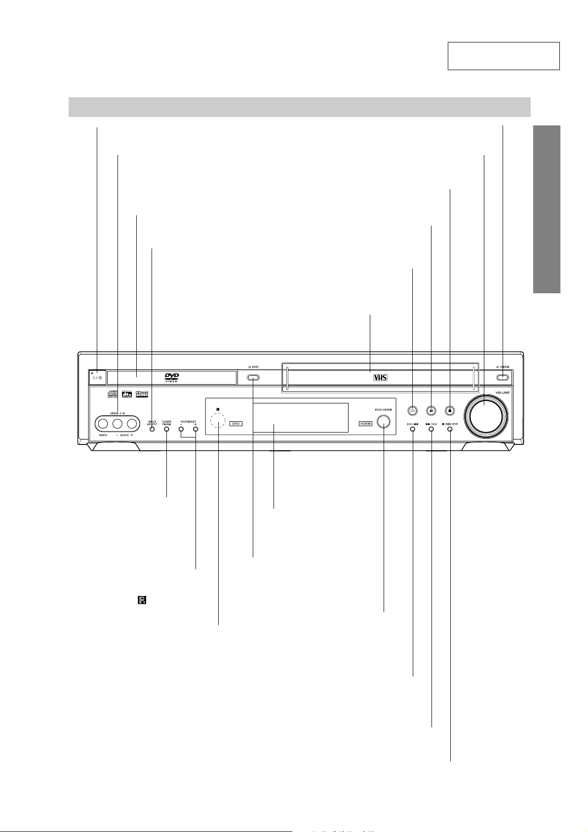
Front Panel
ML
DVD: Go to NEXT chapter/track. Press and hold for a fast forward search.
VIDEO: Advances the tape from STOP mode or for fast forward picture search.
X (PAUSE)
Pause playback or recording
temporarily.
z REC/ITR
To record normally or to activate Instant Timer Recording.
A DVD
Opens or closes
the disc tray.
Remote Sensor
Point the DVD/VCR Receiver remote
control here.
Display window
Shows the current status of the DVD/VCR
Receiver.
Disc Tray (DVD deck)
Insert a disc here.
@ / 1
Switches the DVD/VCR Receiver ON and OFF.
lm
DVD: Go to beginning of current chapter/track or to previous chapter/track.
Press and hold for a fast reverse search.
VIDEO: Rewinds the tape from STOP mode or for fast reverse picture search.
H (PLAY)
To play back a disc or
a recorded tape.
x (STOP)
Stops playback or recording.
INPUT SELECT
Selects the VIDEO deck’s
source (Tuner, VIDEO 1
or VIDEO 2).
CH/PRESET (+/–)
Scans up or down through
memorized channels or radio
frequencies (stations).
TUNER FM/AM
Selects Radio opera-
tion mode.
VIDEO 2 IN(VIDEO/AUDIO IN (Left/Right))
Connect the audio/video output of an
external source (Audio system, TV/ Monitor,
another VCR).
Video Cassette Compartment (VIDEO deck)
Insert a video cassette here.
A VIDEO
Ejects the tape in the VIDEO deck.
VOLUME
Adjusts sound level of speakers.
DVD/VIDEO
Toggles control
between the DVD deck
and the VIDEO deck.
SECTION 1
GENERAL
AVD-K600P
This section is extracted
from instruction manual.
5
Page 6
AVD-K600P
9
INTRODUCTION
VIDEO
Select the output source to VIDEO.
DVD
Sets the output source to DVD.
INPUT SELECT
Selects the VIDEO deck’s source
(L1 OPT, LINE1, LINE2, Tuner).
TUNER FM/AM
Selects the DVD/VCR Receiver’s tuner as
the listening choice. (FM and AM bands)
0-9 numerical buttons
Selects numbered options in a menu.
TUNING (+/–)
To tune in the desired station.
MEMORY
Memorize a radio station frequency into
the tuner.
SHUFFLE
Plays tracks in random order.
PROGRAM
Enters to the program edit mode or exits
from that.
z REC/ITR
Records normally or activates Instant
Timer Recording.
TV/VIDEO
To view channels selected by the VIDEO
tuner or by the TV tuner.
SP/EP
Selects recording speed.
CM SKIP
Fast forwards picture search through 30
seconds of recording.
ANGLE
Selects a DVD camera angle if available.
SUBTITLE
Selects a subtitle language.
AUDIO
Selects an audio language (DVD) or an
audio channel (CD).
REPEAT
Repeat chapter, track, title, all.
A-B
Repeats sequence.
SETUP/MENU
Accesses or returns DVD setup menu
and VIDEO setup menu.
TV @ / 1
Switches TV ON and OFF.
@ / 1
Switches DVD/VCR Receiver ON and OFF.
TV Control Buttons (see page 40)
• VOL +/–: Adjusts TV’s volume.
• CH +/–: Selects TV’s channel.
• TV/VIDEO: Selects the TV’s source.
CLEAR
Removes a track number on the program
menu. To clear preset stations from the
tuner memory.
Playback Control Buttons
• H (PLAY)
Starts playback.
• x (STOP)
Stops playback.
• . (PREV) (DVD mode only)
Go to beginning of current chapter or
track or go to previous chapter or track.
• > (NEXT) (DVD mode only)
Go to next chapter or track.
• m/M (SLOW t/T)
DVD: For picture search or slow playback backward or forward.
VIDEO: Rewinds or advances the tape
in STOP mode or for picture search.
• X (PAUSE)
Pause playback or recording temporarily.
SOUND FIELD
Selects sound mode between BYPASS,
PRO LOGIC, PRO LOGIC II (MOVIE,
MUSIC, MATRIX) and 3D SURROUND.
VOL (+/-)
Adjusts speaker volume.
MUTING
Momentarily silence the speaker of the
DVD/VCR Receiver.
DVD TOP MENU
Displays the disc’s Title menu, if available.
DVD MENU
Accesses menu on a DVD disc.
B/b/V/v (left/right/up/down)
Selects an option in the menu.
CH/PRESET(+/–): Selects a program of
VIDEO or Tuner. Adjusts manually the
tape’s picture onscreen.
ENTER
Acknowledges menu selection.
DVD DISPLAY, CLK/CNT
Accesses On-Screen display. Switches
among the clock and tape counter.
RETURN
Returns the setup menu.
Note
This remote control uses the same buttons for VIDEO and DVD
functions (ex. PLAY).
To use the VIDEO, first press the VIDEO button.
To use the DVD, first press the DVD button.
Remote Control
6
Page 7
AVD-K600P
Rear Panel
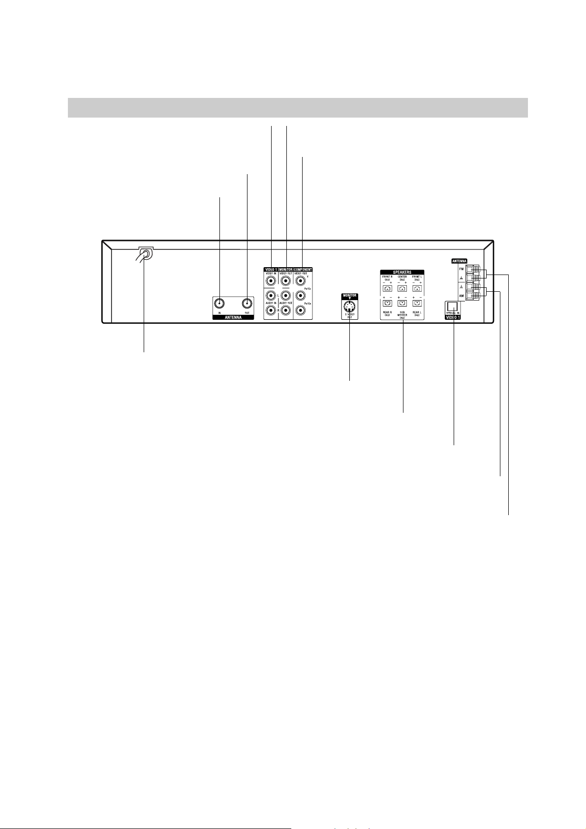
VIDEO 1 (VIDEO/AUDIO IN (Left/Right))
Connect the audio/video output of an external
source (Audio system, TV/Monitor, Another VCR).
ANTENNA IN
Connect the VHF/UHF/CATV
antenna to this terminal.
MONITOR (VIDEO / AUDIO OUT (Left/Right))
Connect to a TV with video and audio inputs.
AC Power Cord
Plug into the power source.
MONITOR S VIDEO OUT (DVD OUT)
Connect to a S Video Input on TV. FOR DVD VIEWING ONLY.
OPTICAL IN
Connect to a digital audio output on a digital device.
COMPONENT VIDEO OUT (Y P
B/CBPR/CR
)
(DVD OUT)
Connect to a TV with Y P
B/CBPR/CR
inputs. FOR DVD
VIEWING ONLY.
ANTENNA OUT (DVD/VIDEO OUT)
Connect to a TV with RF coaxial inputs.
AM ANTENNA Connectors
Connect the AM antenna to this terminal.
FM ANTENNA Connectors
Connect the FM antenna to this terminal.
SPEAKERS Connectors
Connect the six supplied speakers to these terminals.
7
Page 8
AVD-K600P
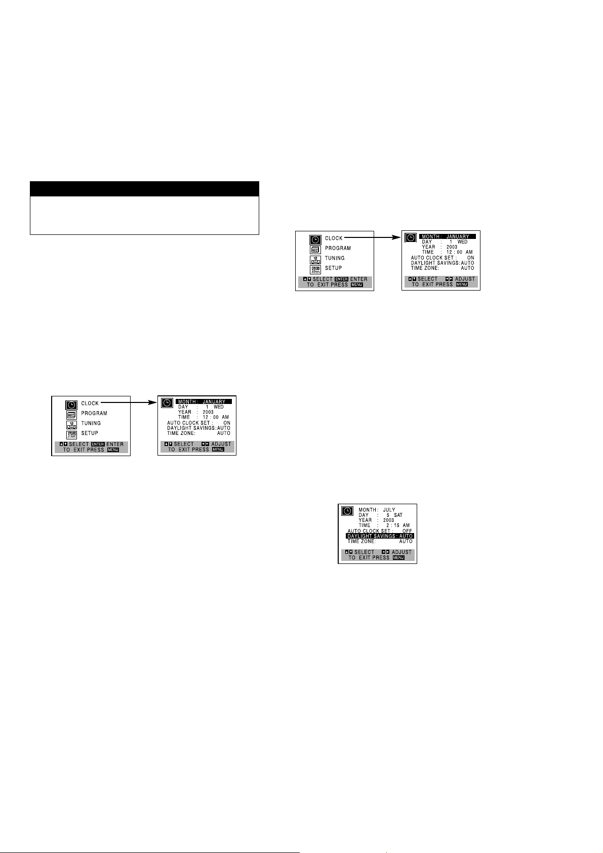
Setting the Clock
The DVD/VCR Receiver gives you two ways to set the
time and date: the Auto Clock Feature or manually. The
Auto Clock feature enables the DVD/VCR Receiver to
set up the clock while the DVD/VCR Receiver is turned
off.
Things to know before starting
•
The clock uses the 12-hour system. (Be sure to set AM
and PM correctly.)
•
The initial Clock Setting is JANUARY 1, 2003, 12:00 AM.
Auto Clock Set
The Auto Clock Set feature is set to ON at the factory. In the
ON setting, the DVD/VCR Receiver looks for a channel carrying XDS (Extended Data Services) information. XDS updates
the clock using the Coordinated Universal Time.
The Auto Clock feature enables the DVD/VCR Receiver
to set up the clock while the DVD/VCR Receiver is
turned off.
Press SETUP/MENU and the MAIN menu will
1
appear.
V v
Use / to select the CLOCK menu.
2
Press ENTER and the CLOCK menu will appear.
v
to select the AUTO CLOCK SET option.
Use
3
4
5
B b
Use / to select ON.
The Auto Clock Set feature is set to ON at the factory. In
the ON setting, the DVD/VCR Receiver looks for a channel carrying XDS (Extended Data Services) information.
XDS updates the clock using the Coordinated Universal
Time.
v
Use to select the DAYLIGHT SAVINGS option.
B b
Use / to select AUTO, ON, or OFF.
If you select AUTO, the DVD/VCR Receiver sets the clock
using the DST information broadcast in the signal (channel). If you select ON, the DVD/VCR Receiver adjusts the
clock for Daylight Saving Time automatically.
v
Use to select the TIME ZONE option.
B b
Use / to select the correct time zone (AUTO,
EASTERN, CENTRAL, MOUNTAIN, PACIFIC,
ALASKA or HAWAII).
If “AUTO” is selected as the time zone, the DVD/VCR
Receiver sets the clock using the first Coordinated
Universal Time information it finds in a broadcast signal.
Press SETUP/MENU to return to the TV screen.
6
Turn off the DVD/VCR Receiver and the auto
7
clock set feature sets the time.
Note
There are cases where the TV station does not send or sends
the wrong time. Therefore, the incorrect time will be set. If this
happens we recommend that you set the clock manually.
Manual Clock Set
Press SETUP/MENU and the MAIN menu will
1
appear.
V v
Use / to select the CLOCK menu.
2
Press ENTER and the CLOCK menu will appear.
B b
Use / to select the month.
3
v
Use to select the DAY option.
4
5
6
7
B b
Use / to select the date.
The day of the week will display automatically.
v
Use to select the YEAR option.
B b
Use / to select the year.
v
Use to select the TIME option.
B b
Use / to select the time.
Press and hold / to advance clock
continuously.
v
Use to select the DAYLIGHT SAVINGS option.
B b
Use / to select AUTO, ON, or OFF.
If you select AUTO, the VIDEO sets the clock using the
DST information broadcast in the signal (channel).
If you select ON, the VIDEO adjusts the clock for Daylight
Saving Time automatically.
Press SETUP/MENU to return to the TV screen.
B b
8
Notes
•
If setting the clock manually, “AUTO CLOCK SET”
must set to “OFF”. If set to “ON”, an incorrect date
and/or time will be entered again when the DVD/VCR
Receiver is turned off.
•
“--:-- --” appears in the display window during clock
setting.
8
Page 9

SECTION 2
s
DISASSEMBLY
• The equipment can be removed using the following procedure.
SET
COVER, FRONT PANEL ASSEMBLY
AVD-K600P
DISPLAY/ KEY BOARD
VCR BOARD DVD & AMP BOARD
Note: Follow the disassembly procedure in the numerical order given.
SMPS BOARD VIDEO MECHANISM DECK DVD MECHANISM DECK
2-1. COVER, FRONT PANEL ASSEMBLY
1
two screws
4
cover
2
three screws
6
three hooks
7
three hooks
5
volume knob
8
front panel assembly
3
two screw
9
Page 10
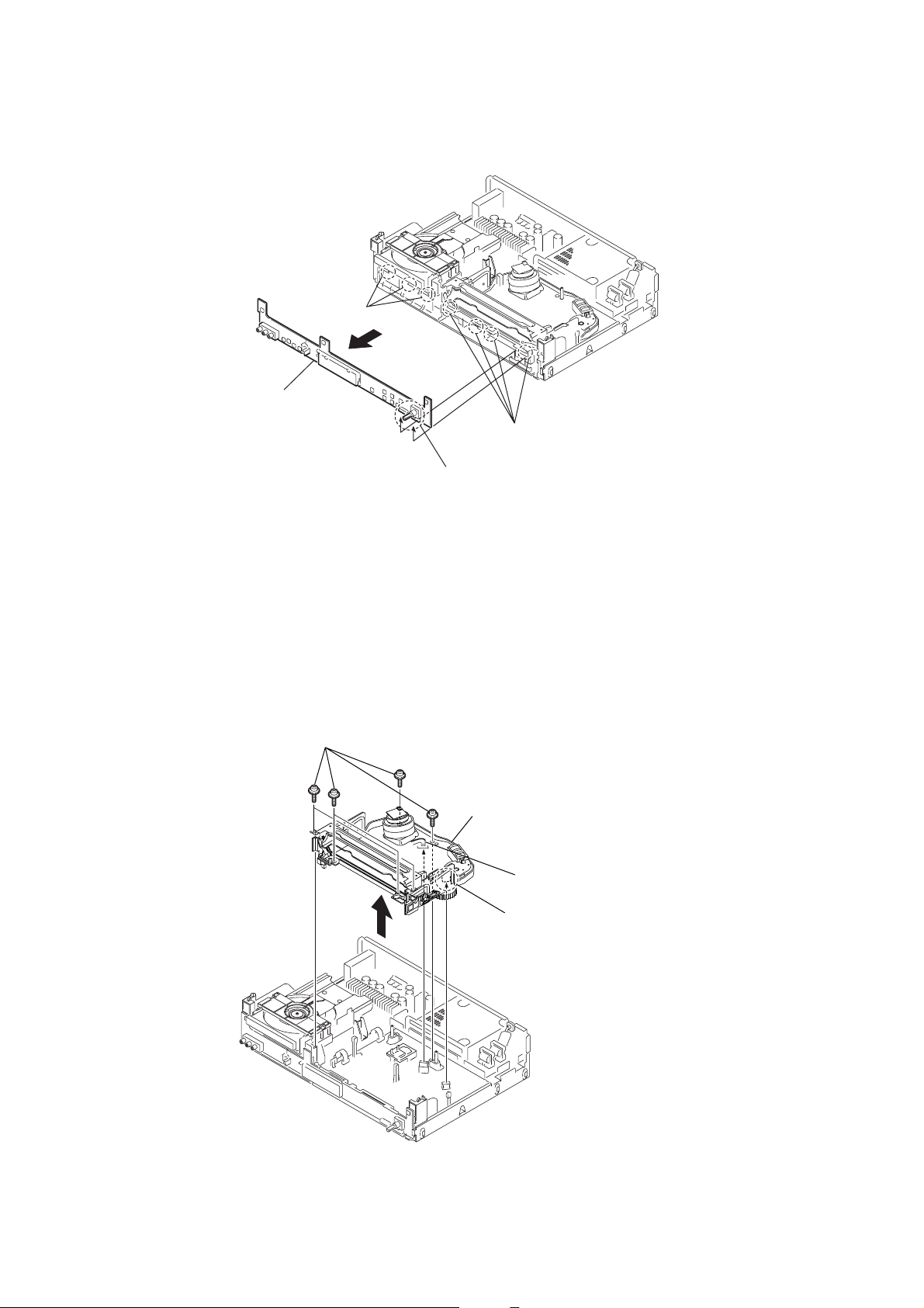
AVD-K600P
k
2-2. DISPLAY/KEY BOARD
4
DISPLAY/ KEY board
1
t
hree claws
2
four
3
connector
(
PM602,PM601
claws
)
2-3. VIDEO MECHANISM DECK
1
s
ix screws
4
VIDEO m
echanism dec
2
fl
exible cable
3
connector
PMCO1
(
)
10
Page 11
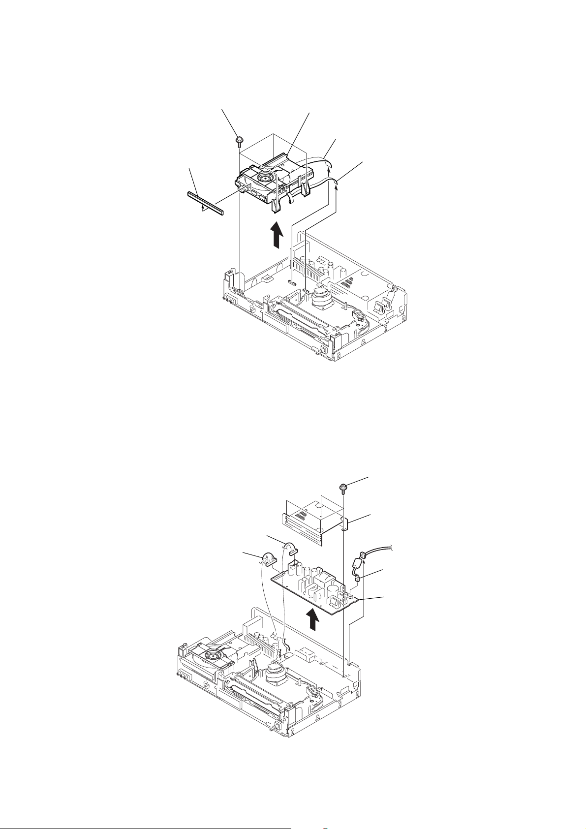
2-4. DVD MECHANISM DECK
)
2
door case
1
four screws
5
DVD mechanism deck
3
flexible cable (PMD01)
4
flexible cable (PMD03)
AVD-K600P
2-5. SMPS BOARD
4
connector (PSW01)
5
connector (PSV01)
1
four screws
2
shield
3
connector (PW101
6
SMPS
board
11
Page 12
AVD-K600P
)
)
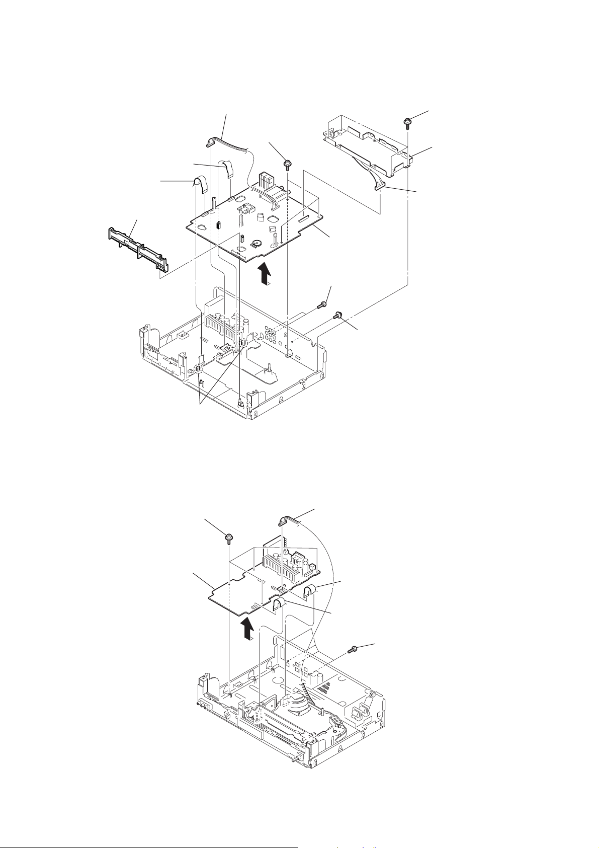
2-6. VCR BOARD
7
8
flexible cable (PVD03)
5
VCR-DISPLAY pwb
flexible cable (PVD02)
holder
6
connector (PDV01)
q;
three
screws
qs
VCR
9
two screws
board
1
four
screws
4
bracket
2
connector (PVS01
2-7. DVD & AMP BOARD
6
qa
two claws
4
four screws
DVD & AMP board
3
1
connector (PDV01)
2
flexible cable (PDV02
3
flexible cable (PDV03)
screw
12
5
four screws
Page 13
SECTION 3
ELECTRICAL ADJUSTMENT
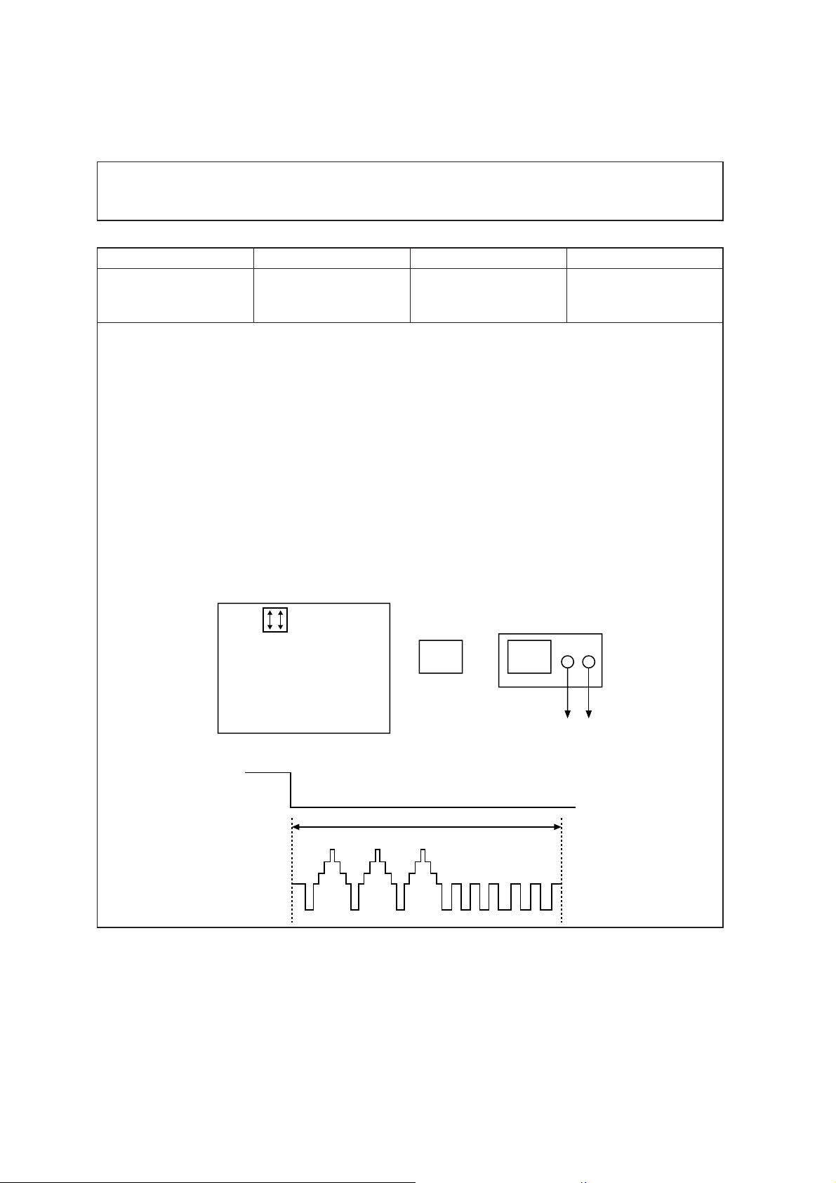
3-1. VCR SECTION ELECTRICAL ADJUSTMENT
1. Servo Adjustment
1) PG Adjustment
• Test Equipment
a) OSCILLOSCOPE
b) NTSC MODEL : NTSC SP TEST TAPE
• Adjustment And Specification
AVD-K600P
MODE
PLAY
MEASUREMENT POINT ADJUSTMENT POINT SPECIFICATION
V.Out
H/SW(W373, W374)
R/C TRK JIG KEY 6.5 ± 0.5H
• Adjustment Procedure
a) Insert the SP Test Tape and play.
b) Connect the CH1 of the oscilloscope to the H/SW(W373, W374) and CH2 to the Video Out for the VCR.
c) Trigger the mixed Combo V ideo Signal of CH2 to the CH1 H/SW(W373, W374), and then check the dis-
tance (time difference), which is from the selected A(B) Head point of the H/SW(W373, W374) signal to
the starting point of the vertical synchronized signal, to 6.5H ± 0.5H (412µs, 1H=63µs).
Note - Press FRONT CH UP KEY and FRONT PLAY KEY on Deck playback, and it goes in to ATR PRE-
SET. after the SP Test Tape is inserted.
• PG Adjustment Method
a-1) Payback the SP standard tape
b-2) Press the “O” key on the Remote controller and the “PLAY” key on the Front Panel the same time,
then it goes in to Tracking initial mode.
c-3) Repeat the above step(No.b-2), then it finishes the PG adjusting automatically.
d-4) Stop the playback, then it goes out to PG adjusting mode after mony the PG data.
• CONNECTION
V.Out
OSCILLOSCOPE
H/SW(W373, W374)
CH1 CH2
•WAVEFORM
H/SW
Composite
VIDEO
6.5H(412µs)
R/C KEY
V.out
H/SW
(W373, W374)
13
Page 14
AVD-K600P
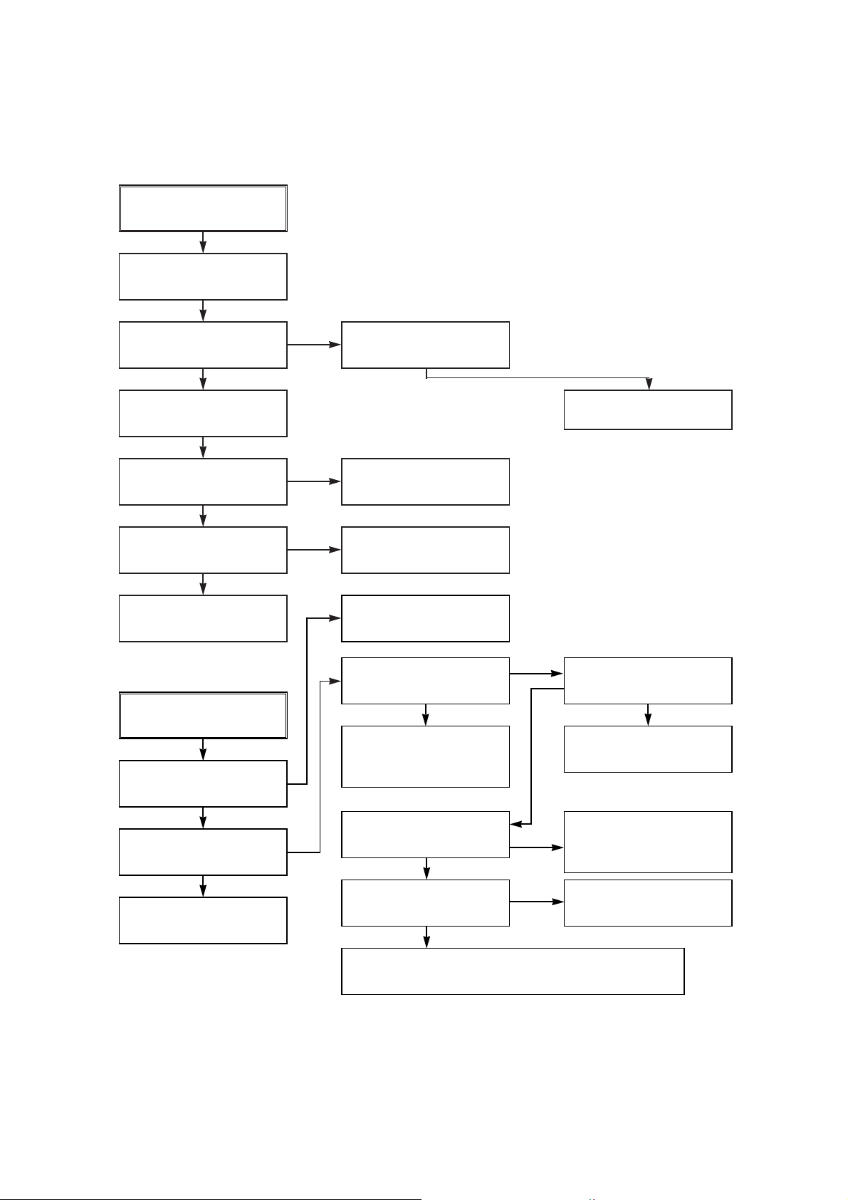
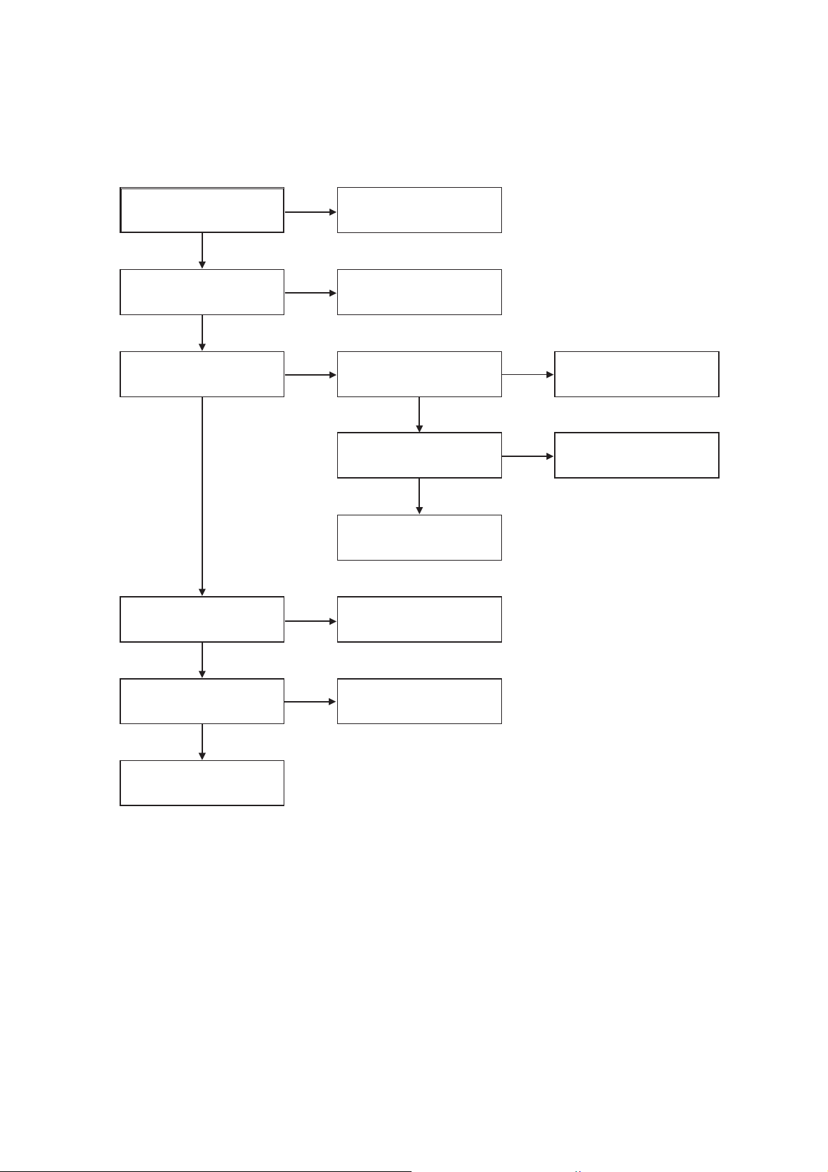
3-2. ELECTRICAL TROUBLESHOOTING GUIDE
1. Power (SMPS) CIRCUIT
(1) No 5.3VA (SYS/Hi-Fi/TUNER)
NO 5.3VA.
YES
Is the F101 normal?
YES
Is the BD101
NO
NO
Replace the F101.
(Use the same Fuse)
normal?
YES
Is the R101
normal?
YES
Is Vcc(8.5~21V) sup-
NO
NO
Replace the R101.
plied to IC101 Pin7?
YES
Check or Replace
the D102.
Replace the
BD101.
Is the D102
normal?
NO
(2) No 12VA (TO CAP, DRUM MOTOR)
NO 12VA.
YES
Is the Vcc(13V) supplied
NO
to (+) terminal in D115?
YES
Is the Vcc(12V) supplied
NO
to (-) terminal in D115?
YES
Check or Replace
the D110.
Replace the D115.
Check or Replace
the Motor Vcc.
(3) No 5.0V (SYS/Hi-Fi/TUNER)
Is the D112 normal?
YES
Is there about 2.5V
at the IC103 Vref?
YES
Check the Main PCB
5.3VA/5.0V Line short?
NO
NO
Replace the D112.
Replace the IC103.
NO 5.0VA.
YES
Is 5.3VA put into
the Q160 Emitter?
YES
Is the Q162 Base
“H”?
YES
Is about 5V put into
the Q160 Base?
YES
Check or Replace
the Q162/Q160.
NO
NO
NO
5.3VA Line Check.
Check the Power
Control.
Check or Replace the
Q162, R157, R158, R159.
14
Page 15
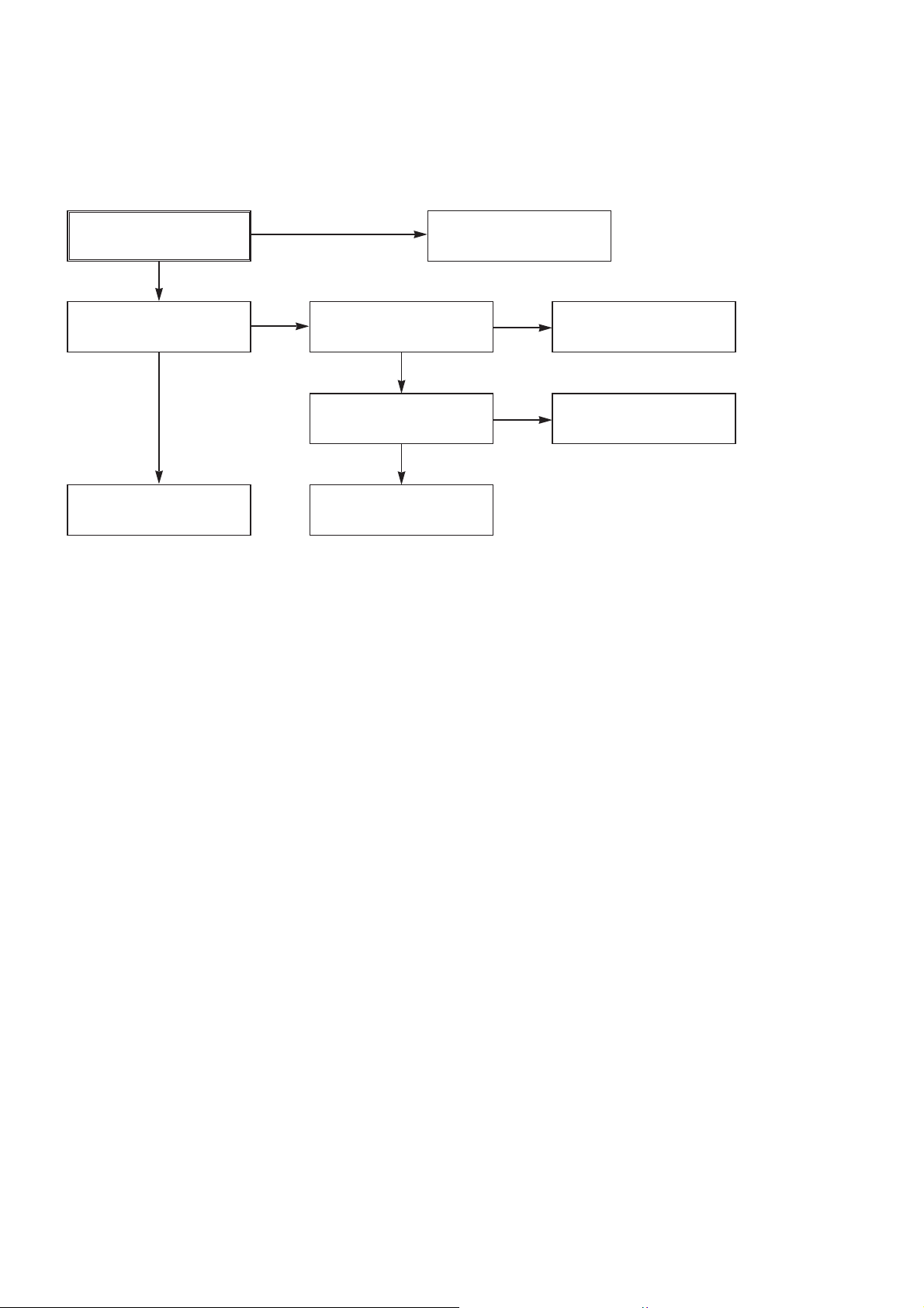
AVD-K600P
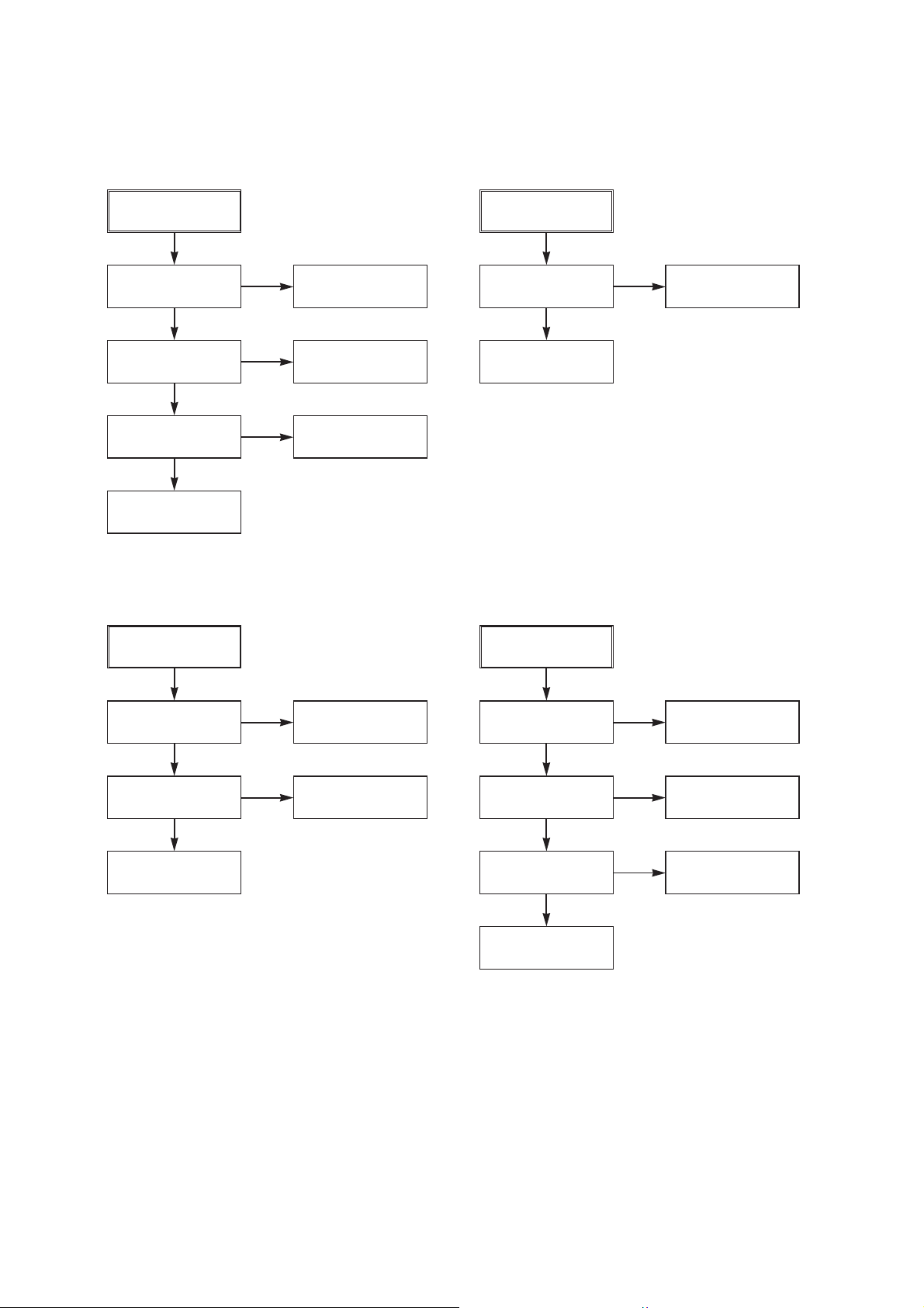
(4) No 5V (TO DVD)
NO 5V.
YES
Is 5.3VA put into
the Q160 Emitter?
YES
Is the Q162 Base
“H”?
YES
Is about 5V put into
the Q160 Base?
YES
Check or Replace
the Q162/Q160
(6) No REG 12V
NO
NO
NO
5.3VA Line Check.
Check the Power
Control.
Check or Replace the
Q162, R157, R158, R159.
(5) No 33V (TUNER)
No 33V.
YES
Is Q163 Base “H”?
YES
Check or Replace
Q161, R154, R155.
(7) No 8V(TO DVD)
NO
Check the Power
Control.
No REG 12V.
YES
Is 13V put into the
NO
Q156 Collector?
YES
Is 13V put into the
NO
R153 Base?
YES
Check or Replace the Q156,
ZD103, R153, C151.
Check or Replace
D110.
Check 33V Line.
NO 8V.
YES
Is Vcc(13V) supplied to
(+) terminal in D114?
YES
Is Vcc(12V) supplied
to IC151 Pin1?
YES
Is the Q162 Base
“H”?
YES
Check or Replace
IC151, R170, C154.
NO
NO
NO
Check or Replace
the D110.
Check or Replace
the D114.
Check the Power
Control.
15
Page 16
AVD-K600P
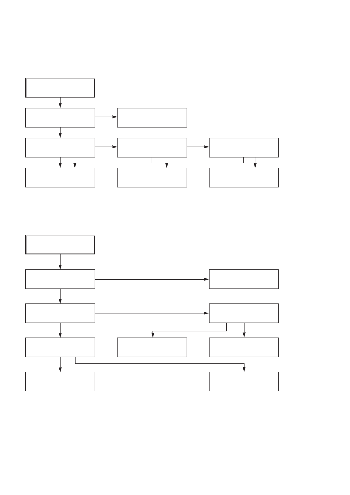
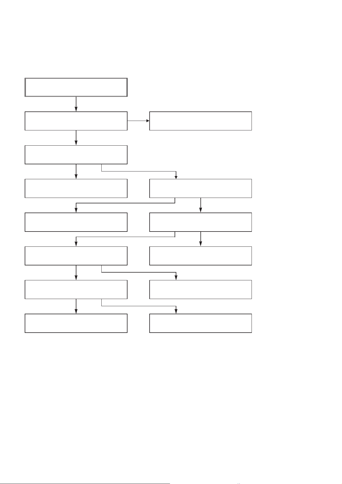
2. SYSTEM/KEY CIRCUIT
(1) AUTO STOP
Auto Stop
YES
Does the SW30 waveform
appear at the IC501
Pin18?
YES
Do the T-UP Reel Pulses
appear at the IC501 Pin80?
YES
NO
NO NO
Check the Drum Motor
signal.
Do T/UP Reel Pulses
appear at the point
between R556 and R536?
YES YES
Does 5V appear at the
RS501?
NO
Replace the IC501.
Replace the T/UP Reel
Sensor (RS501).
(2) The unstable loading of a Cassette tape
The unstable loading of a
Cassette tape
YES
Is 12V applied to the
PMC01 Pin8?
YES
Does the “H” signal appear
at the IC501 Pin60 during
inserting the CST ?
YES
Does the “L” signal appear
at the IC501 Pin19 during
inserting the CST?
YES
NO
NO
Check the CST SW and
the peripheral circuitry.
NO
Check the Q160 Power
Circuit.
Refer to “SMPS DRUM
12 Volt Trouble Shooting”.
Is 5V applied to the
R531 ?
YES
Refer to SMPS 5.3VA
troubleshooting.
NO
Caution :
16
Check the Deck
Mechanism.
Auto stop can occur because Grease or Oil is dried up
Check the IC501
Pins22, 23, 24, 25.
Page 17
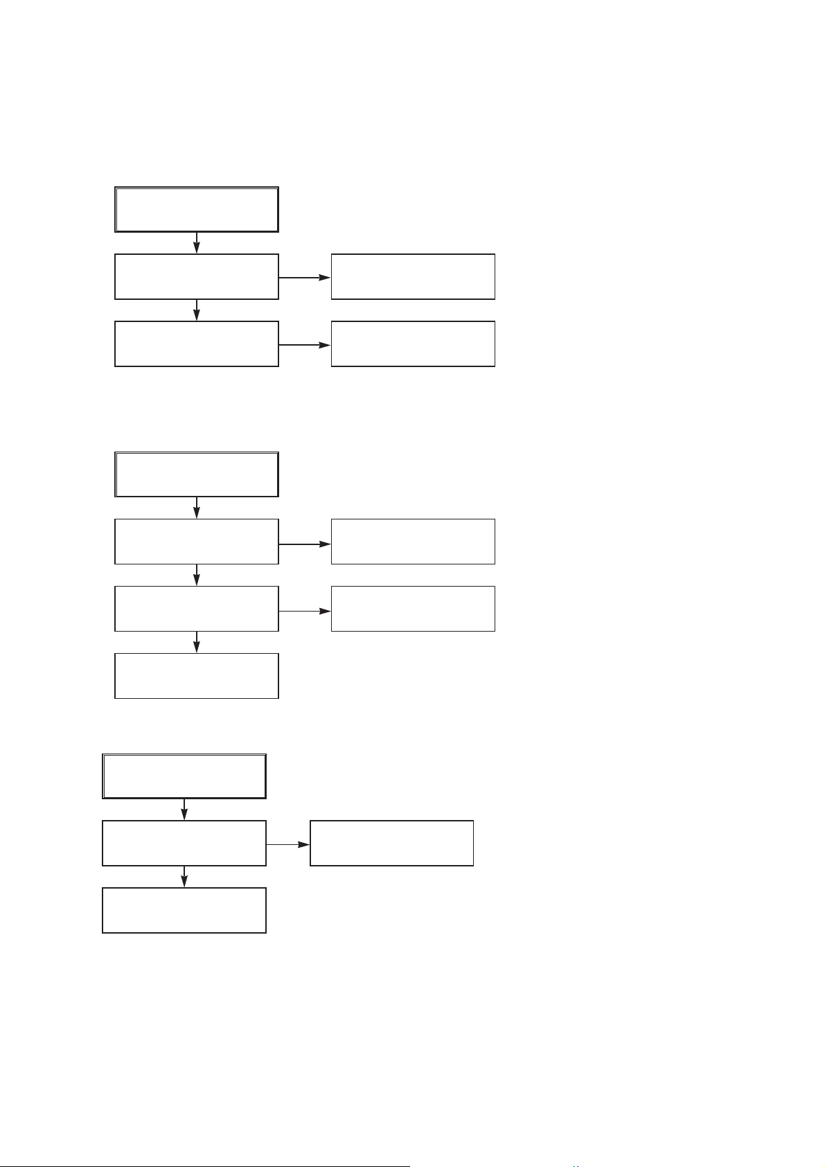
3. SERVO CIRCUIT
(1) Unstable Video in PB MODE
Unstable Video in
PB Mode.
YES
Does the Noise level of the
screen change
periodically?
YES
AVD-K600P
Do the CTL pulses appear
at the IC501 Pin97?
YES
Does the CFG waveform
appear at the IC501
Pin87?
YES
On tracking do the CTL
pulses move?
YES
Does the Video Envelope
waveform appear at the
IC501 Pin9?
YES
Replace the IC501.
(2) When the Drum Motor
(2) doesn’t run.
When the Drum Motor
doesn’t run,
Does 12V appear at the
PMC01 Pin8?
NO
NO
NO
NO
Is adjusting the height of
the CTL Head accurate?
Replace the IC501.
Refer to “When the Y signal
doesn’t appear on the
screen in PB Mode”.
Refer to “(2)
No 12VA of Power section”
Do the Drum PWM Pulses
appear at the IC501
Pin76?
YES
Aren’t the foil patterns and
the Components between
IC501 Pin76 and PMC01
Pin12 short?
NO
NO
Readjust the height of the
CTL Head.
Do the DFG Pulses appear
at the PMC01 Pin11?
YES
NO
Replace the Cap M.
YES
Does 2.8V appear at the
PMC01 Pin12?
YES
Check the connector
(PMC01) and the Drum
Motor Ass’y.
NO
Do the DFG Pulses appear
at the IC501 Pin90?
YES
Do the Drum PWM Pulses
appear at the IC501
Pin76?
YES
Aren’t the connecting patterns and the Components
between IC501 Pin76 and PMC01 Pin12 short?
NO
NO
Aren’t the foil patterns and
the Components between
IC501 Pin 90 and PMC01
Pin11 short?
Replace the IC501.
17
Page 18
AVD-K600P
(3) When the Capstan Motor doesn’t run,
When the Capstan Motor doesn’t run,
Does 12VAappear at the PMC01?
YES
Is “DRUM CTL” 2.8V appear at the
PMC01?
YES
Check the PMC01 and the Capstan
Motor Ass’y.
Aren’t the foil patterns and Components
between IC501 Pin77 and PMC01
Pin9 short?
Does the CFG signal come into the
IC501 Pin87?
YES
NO
NO
NO
YES
YES
Refer to “SMPS(CAPSTAN/12Volt)
Trouble Shooting”.
Does the PWM signal appear at the
IC501 Pin77?
NO
Does the CFG signal appear at the
PMC01 Pin1?
NO
Check the Capstan Motor Ass’y.
Does the Capstan PWM signal appear at
the IC501 Pin77?
YES
Aren’t the foil patterns and Components
between IC501 Pin77 and PMC01
Pin9 short?
Aren’t the foil patterns and component
between IC501 Pin87 and PMC01
Pin1 short?
NO
Replace the IC501.
18
Page 19
(4) KEY doesn’t working
KEY doesn’t working.
AVD-K600P
Is 5V applied to the IC501
Pin79?
YES
Does LED or FLD change
when a function button is
pressed?
4. OSD CIRCUIT
(1) No OSD display.
No OSD or F.OSD display.
Is 5.3V applied to the
IC501 Pin53?
YES
Does oscillation occur at
the IC501 Pins44, 45?
YES
NO
NO
NO
NO
Refer to “SMPS 5.3VA
Trouble Shooting”.
Replace the defective
switches.
Refer to “SMPS 5.3VA
Trouble Shooting”.
Check or Replace the pheripheral Circurity.(L511,
R518, C596, C595)
Replace the IC501.
2
(2) I
C BUS CHECK
The I2C waves don’t
come out.
Does Power appear at the
Pull up impedence
(R569, R507)?
YES
Replace the IC501.
NO
Refer to “SMPS 5.3VA
Trouble Shooting”.
19
Page 20
AVD-K600P
5. Y/C CIRCUIT
(1) No Video in EE Mode,
No Video in EE Mode
Does the Video signal
appear at the IC301
Pins28, 30, 32?
YES
Is REG 5.0V applied to the
IC301Pins23, 44, 45, 52, 68,
77?
YES
Does the Video signal
appear at the IC301 Pin26?
YES
Does the Video signal
appear at the IC501 Pin52?
NO
NO
NO
NO
Does the Video signal
appear at the IC302
Pins1, 5?
Is there 5V at the IC302
Pin6?
Replace the IC302.
Check the REG 5V Line.
(Power Circuit)
Is I2C BUS signal applied to
the IC301 Pins53, 54, 55?
Check the path of the signal between the IC301 Pin
26 and IC501 Pins50, 52.
YES
YES
YES
NO
NO
Check DVD Video Input
(IC602, Pin4), Tuner Video
Input (TU701 Pin16), Line
Video Input (JK601),
respectively.
Check the System Circuit.
(Refer to ‘SYSTEM I
CHECK Trouble Shooting’)
Replace the IC301.
2
C BUS
YES
Does the Video signal
appear at the IC602 Pin7?
NO
Is there 5V on the plus
terminal of the C614?
YES
Replace the IC602.
NO
Check the REG 5V Line.
(Power Circuit)
20
Page 21
(2) When the Y(Luminance) signal doesn’t appear on the screen in PB Mode,
AVD-K600P
Is 5V applied to the IC301
Pins23, 44, 45, 52, 68, 77?
YES
Is the Y/C Bus signal
applied to the IC301
Pins53, 54, 55?
YES
Does the normal RF signal
appear at the IC301 Pin14?
YES
NO
NO
NO
Check the line of the REG
5V Line. (Power Circuit)
Refer to ‘SYSTEM Y/C
BUS CHECK Trouble
Shooting’.
Is the V.H.S/W signal
applied to the IC301 Pin57?
YES
Does the Rectangular
waveform(5V) appear at
the IC301 Pin57(V.H.S/W)
YES
Clean the Drum.
NO
NO
Check the System Circuit.
(IC501 Pin18)
Check the V.H.S/W level.
Does the Y(Luminance)
signal appear at the IC301
Pin20?
YES
Is the Y(Luminance) Video
waveform showed up at the
IC301 Pin22?
YES
Replace the IC301.
NO
NO
Check the R328, R347,
C322, C323.
Check the C324.
21
Page 22
AVD-K600P
(3) When the C(Color) signal doesn’t appear on the screen in PB Mode,
Is 5V applied to the IC301
Pins23, 44, 45, 52, 68, 77?
YES
Does the fsc signal appear
at the IC301 Pins41, 50?
YES
Replace the IC301.
NO
NO
Check the line of the REG
5V Line. (Power Circuit)
Is normal the X301
(3.58MHZ) of oscillation
Frequency?
Does the Color signal
appear at the IC301 Pin48?
YES
Replace the IC301.
NO
NO
Replace the X301.
Check the C342, C341,
R333.
22
Page 23
(4) When the Video signal doesn’t appear on the screen in REC Mode,
REC mode
YES
AVD-K600P
Is EE mode normal?
YES
Is brightness normal?
YES
Is the brightness signal supplied to IC301 Pins18?
YES
Check the power of Pins23,
44, 45, 52, 68, 77.
YES
Check the REG 5V power
NO
YES
YES YES
NO
Check the EE mode
Is color
Does signal appear at
IC301 Pins41, 50?
Is 5V supplied to IC301
Pins23, 44, 45, 68, 77?
Is Y/C Bus applied to
IC301 Pins53, 54, 55?
Do X301 and X-TAL
oscillate?
normal?
NO
NO
YES
YES
YES
NO
NO
NO
A
Check X301 oscillation
frequency.
Check the 5V power
Check system part
Check X301.
A
YES
Is V.H SW supplied to
IC301 Pin57?
YES
Does the FM signal appear
at IC301 Pins73(SP)/
66(EP)?
YES
Replace the IC301.
NO
NO
Check system part
(V.H/SW)
Check the drum
*OPTION
Pins72, 73, 74(SP)
Pins65, 66, 67(EP)
23
Page 24

AVD-K600P
6. Tuner/IF CIRCUIT
(1) No Picture on the TV screen
No picture on the TV
screen
YES
Does the Video signal at
the TU701 Pin16.
YES
Does the video signal
appear at IC302 Pin7.
NO
NO
Is +33V applied to TU701
Pin14?
YES
Is +5V applied to TU701
Pin3?
YES
Does the Clock signal
appear at TU701 Pin9?
YES
Does the data signal
appear at TU701 Pin10?
YES
Replace Tuner.
Check the signal flow from
IC501 Pin27.(Pin27 is ‘L’
state in Tuner Mode)
NO
NO
NO
NO
Check 33V line.
Check 5V line.
Check the lIC Clock Signal
of µ-COM Pin71.
Check the lIC Data Signal
of µ-COM Pin72.
YES
Does the Video signal at
the IC501 Pin 52.
YES
Does the Video signal at
the IC602 Pin 7.
YES
Check the signal flow from IC602
Pin7 to JK601 Pin Video out.
NO
NO
Check the signal from IC301
Pin26 to IC501 Pin50.
Check the signal from IC501 Pin52 to IC602 Pin1 and IC602 Pin2.
(IC602 Pin2 is ‘L’ state in VHS mode)
24
Page 25
(2) No Sound
AVD-K600P
No Sound.
YES
Check the Vcc of TU701 Pins3, 14.
YES
Check the Tuner SiF signal at IC801
Pin57.
YES
Check the Audio of IC801 Pins78, 80.
YES
Check the Signal flow from IC801 Pins78,
80 to JK601 Audio out(L), (R)
NO
NO
NO
Check 5.2V, 33V Line.
Check the Tuner SIF of TU701 Pin13.
1. Check the Vcc(5.3VA, 9V) of IC801
Pins3, 5, 36, 54.
2. Check the IIC Clock and Data at IC801
Pins37, 38.
25
Page 26
AVD-K600P
7. Hi-Fi Circuit
A.
Hi-Fi Playback.
No sound
Check the Hi-Fi Selection
Switch and the Tape quality.
YES
Is the RF waveform at
IC801 Pin 23 over 3V
Vp-p?
YES
NO
Is Pin 30 of IC801 over
3.5V ?
Check IC801 Pin 37(Data),
Pin 38(Clock).
YES
NO
YES
Check the Vcc of IC801.
(Pins 3, 15, 32, 46)
YES
YES
Is the Head switching signal
IC801 Pin 39 O.K?
YES
Check the connection at
P3D01 if good then
Replace IC801.
NO
NO
Check power.
Check REC start “H” signal
of µ-COM.
NO
Check IC501 Pin 19.
(Audio Swich 30)
Is IC801 Pin 49(A.Mute)
“High”?
YES
Do Audio signals appear at
IC801 Pin 80(L-CH),
78 (R-CH)?
YES
Check the Contact point
of Audio Output.
Check Ports of µ-COM.
Check A.MUTE port of
µ-COM (Pin High of
IC501).
NO
Replace IC801.
26
Page 27

B.
Hi-Fi REC.
It is impossible to record and playback
Hi-Fi Audio signal.
YES
Check Vcc of IC801. (Pins 3, 15, 32, 46)
AVD-K600P
YES
Check IC801 Pin 37(Data),Pin 38(CLOCK).
YES
Is IC501 Pin 84(A.Mute) “High”?
YES
Are Audio signals present at IC801
Pins 78, 80?
YES
Do FM Audio signals appear at IC801
Pin 26?
YES
Is IC801 Pin 17(REC “H”) “High”?
YES
NO
Check Power.
NO
Check ports of µ-COM.
NO
Check the Port of µ-COM.
NO
Check Audio Input signal Line
(9, 11, 12, 71, 73, 74), Tuner(57).
NO
Replace IC801.
NO
Check the Contact Points of Drum
Connector if good then Replace the Drum.
Check the Port of u-COM.
27
Page 28

AVD-K600P
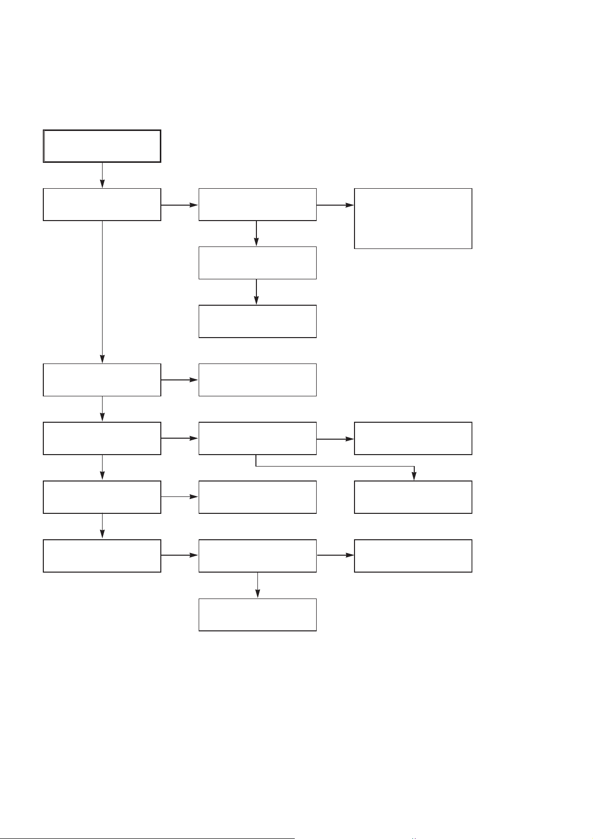
3-3. DVD & AMP SECTION ELECTRICAL TROUBLESHOOTING GUIDE
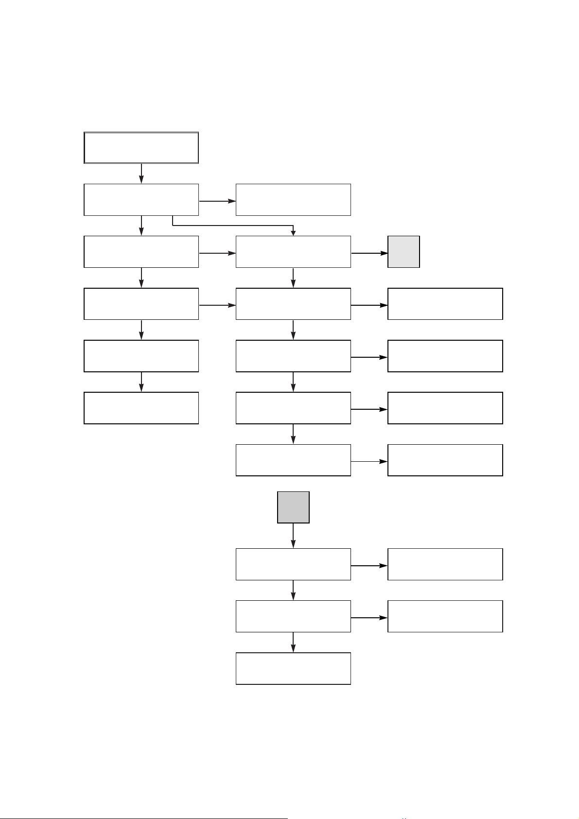
1. System operation flow
Power On
1. 8032 initializes SERVO, DSP & RISC registers
2. Write RISC code to SDRAM
3. Reset RISC
Show LOGO
Yes
SLED Moves to Inner Position
1. Judge whether have disc and disc type
2. Jump to related disc reading procedure
Tray Closed?
No
Tray Close to Closed position
SLED at Inner
Side?
No
Recieve
OPEN/ CLOSE
Key?
Yes
No
1. Execute Pressed Key & IR Key
2. Systemoperati on Routi ne Loop
1. Stop Playback & Open Tray
2. Display tray open message & LOGO
No
Receive
CLOSE Key?
28
Yes
Page 29

2. Test & debug flow
TEST
AVD-K600P
Check the
AC Voltage
Power PCBA (110V
or 220V)
Yes
Switch on the Power PCBA
Is
the DC Voltage
outputs OK?
(5V, 3.3V, 8V, 12V)
Yes
Is 3.3V and 2.5V DC
outputs normal on main
Communication between
VCR & DVD is normally?
PCBA?
Yes
Yes
No
No
No
No
Check the POWER PART
Check the POWER PART
Check the regulators or diode(D501).
Check the cable connection.
(PDV03)
Connect to PC RS232 Cable and
update the FLASH memory code.
Update
FLASH(IC5A1)
successfully?
Yes
A
No
1. Check 27MHz system clock.
2. Check systemreset circuit.
3. Check FLASH R/Wenable signal PRD,
RWR.
4. Check RS232 SIGNALS.
5. Check FLASH Memory related circuit.
Replace FLASH( IC5A1)
29
Page 30

AVD-K600P
A
RESET or Power On.
Show LOGO?
YES
NO NO
Flash
Memory operates
properly?
YES
SDRAM
works properly?
NO
YES
MT1379
VIDEO outputs
properly?
NO
YES
Have
TV signal output?
NO
YES
Check AV cable
connection to TV set .
Check connection lines between FLASH
& MT1379 and the FLASH access time
whether is sui table or not.
Check connection lines between
SDRAM(IC502,IC503) & MT1379 and the
SDRAM is damaged.
Check the related circuit of MT1379.
(IC501 PIN 161,166, 168 check)
Check the filtering and amp circuit of
TV signal .(IC507)
Does
Tray move inside
when it is not at
closed position?
YES
B
NO
Normal
TROUT & TRIN
signals?
YES
Normal
TRCLOSE &
TROPEN signal?
YES
Normal
LOAD+ & LOAD-
signal ?
YES
Check the cable connection between
main PCBA and loader. (MECHA)
NO
NO
NO
Check the load OPEN &
CLOSE switch
Check the Tray control IO pins
on MT1376 & MT1379.
Check the Tray control amplifying
circuit on Motor driver.(IC402)
30
Page 31

B
Does
the SLED move
to inner side when it is at
outer position?
No
Motor Driver STBY
Pin is High?
No
AVD-K600P
Check the connection line of
STBY signal .
Do not put in disc and tray
close.
Yes
Motor Driver STBY
Pin is High?
Yes
SL+ and SL- output
properly?
Yes
Check the cable connection
with MECHA.
No
No
OKYes
Check the related circuit of
FMSO.
Check the amp circuit on
motor driver.
Optical
Lens has movements
for searching
Focus?
Yes
C
Proper FOSO outputs
to motor driver?
Yes
Proper F+
& F- outputs?
Yes
Check cable connect of the
pick-up head.
NoNo
No
Check FOSO connection on
MT1379 and motor driver.
Check the amp circuit on
motor driver.
31
Page 32

AVD-K600P
C
Laser turns on when
reading disc?
Yes
Disc ID is correct?
Yes
Does spindle rotate?
No
No
No
LD01 or LD02 output
properly?
Yes
Collector
voltage of power
transistor is OK?
(Q404, Q405)
Yes
Check cable connection between
transistor output and pick-up head.
Proper RFL signal
on MT1336?
Yes
Check the RFL connection
between MT1336 and MT1379.
Proper
DMSO signal on
MT1379
No
No
No
No
Check the laser power circuit
on MT1336 and connecting to
power transistor. (Q404, Q405)
Check the related circuit on
laser power transi stor
Check the related circuit
on MT1336 RFL signal .
Check DMSO related
circuit on MT1379.
D
Yes
Yes
SP+ & SP- output
properly?
Yes
Check the cable connection
between spindle and main PCBA.
No
Check the spindle control
amp circuit of motor driver.
32
Page 33

D
AVD-K600P
Yes
Focus ON OK?
Yes
Track On OK?
Yes
No No
Check FEO connection
between MT1336 and MT1379
Proper
signals on A, B, C,
D of MT1336
Yes
Proper FEO signal
on MT1336?
Yes
Proper FEO signal
on MT1336?
Yes
Properly TRSO signal
on MT1379?
Yes
No
NoNo
No
Check connections between
MT1336 and pick-up head.
Check the related circuit
on MT1336 FEO sugnal .
Check the related
circuit on MT1336
Check the TRSO connection
on MT1379 and motor dirver.
Disc is play?
Yes
E
No
T+ & T- output
properly?
Yes
Check cable connection on
pick-up head.
Check RF signal waveform.
No
Check the tracking control
amp circuit on motor driver.
33
Page 34

AVD-K600P
E
Normal
Audio output
when disc playback?
YES YES
TEST END
NO
Audio
DAC received
correct data stream?
Normal
Audio DAC
out? (IC206)
YES
Check Audio filter, amplify, mute
circuit. (IC205 Application circuit)?
NO
NO
Check connection between MT1379
& Audio DAC. (Check ARCK, ALRCK
ACKL, ASDAT3)
Check the related circuit of
Audio DAC. (Check Audio
out Pins 8, 5)
34
Page 35

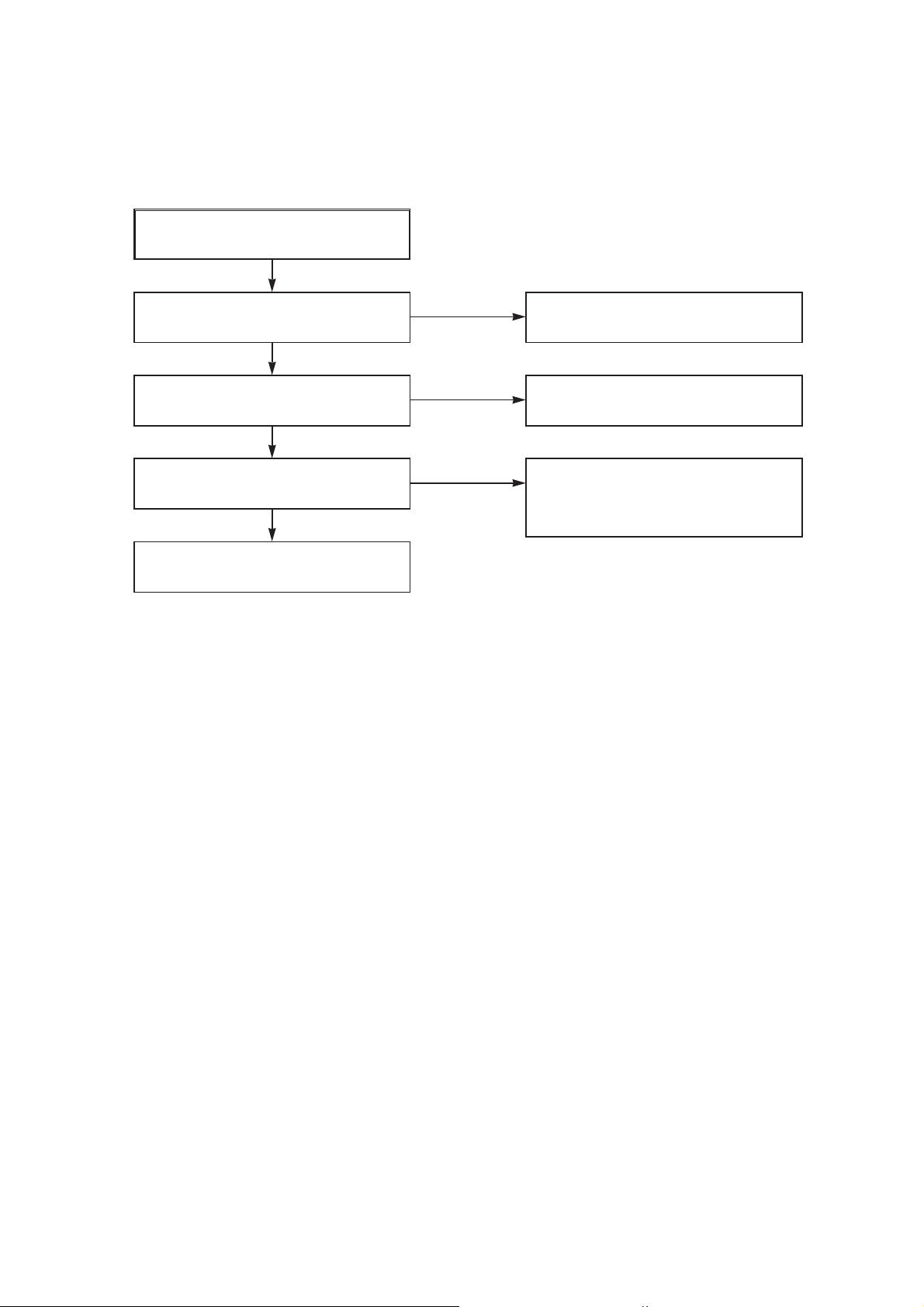
3. AUDIO µ-COM Circuit(DVD & AMP)
POWER ON
AVD-K600P
Does CD/DVD appear
at FLT?
YES YES
Does Loading appear
at FLD?
YES
Does no Dise or Time
appear at FLD?
YES
YES
Check if DVD an Audio
Micom Insert is OK.
YES
Check Power.
YES
Check DVD Module.
NO NO
NO
Does it appear DVD Error
at FLD?
NO
Check Connector (DVV01)
if is normally.
Check power part of Main
B/D.
NO
Check oscillator of X101.
Check if PN102 is high.
YES
YES
YES
YES
NO
NO
NO
NO
NO
Does CD/DVD appear
at FLT?
Reconnet it.
Refer to SMPS.
Refer to oscillator Circuit.
Check DVD Reset
Waveform.
OK
Check SMPS.
YES
Check if IC101 Pin53
is high.
YES
Check if IC101 Pin9, 36,
59 is high(5V).
YES
Check if IC101 Pin49
is high.
YES
Replace IC101.
NO
NO
NO
Check IC101 Reset
Waveform.
Check 3.3V line.
Check Power dection
Circuit.
35
Page 36

AVD-K600P
SECTION 4
MECHANICAL ADJUSTMENT
4-1. VIDEO MECHANISM DECK SECTION
• Tools and Fixfures for Service
1. Cassette Torque meter
SRK-VHT-303(Not SVC part)
300
S
-
T
250
H
V
-
200
K
R
150
S
S
R
K
V
I
D
E
O
C
A
S
V
-
S
K
E
R
T
T
T
S
E
O
50
R
0
Q
U
E
M
E
T
E
R
V
H
T
-
3
0
3
4. Torque gauge adaptor
2. Alignment tape
(See figure below)
H
T
-
T
0
50
100
150
200
250
300
5. Post height adjusting driver
3. T orque gauge
600g.Cm ATG
6. + Type driver (φ 5)
Parts No.: SV-TGO-030-000(SMALL)
: SV-TGO-030-000(LARGE)
• Alignment Tapes for Adjustment
Derivation No.
Mechanism
Adjustment Items
FM Envelope
Slantness
A/C
Head
Height
Azimuth
X-value
RG Post Inclination
Tape Back Tension
ABCD
ABCD
SP/LP SP SP/LP/EP SP
2/4 Head 2 Head 2/4 Head 2 Head
TTV-P2L TTV-P2 TTV-N2
A commecially available tape
TTV-P1 TTV-N1
(TTV-P1L) (TTV-N12)
TTV-P1 TTV-P2 TTV-N2 TTV-N2
TTV-P2
(TTV-P2L)
A commecially available tape
TTV-N1
(TTV-N12)
TTV-N1
TTV-P1 (TTV-N12)
(TTV-N1E)
TTV-N2
TTV-P2 TTV-N2E TTV-N2
TTV-N12
SRK-VHT-303
The numbers in ( ) parenthesis can be used as the substiture.
36
Page 37

AVD-K600P
1. Mechanism Alignment Position Check
Purpose:To determine if the Mechanism is in the correct position, when a Tape is ejected.
Test Equipment/ Fixture
• Blank tape
1) Turn the Power S/W on and eject the Cassette by pressing the Eject Button.
2) Remove the Top Cover and Plate Assembly Top, visually check if the Gear Cam Hole is aligned with the
Chassis Hole as below Fig. C-2.
3) IF not, rotate the Shaft of the Loading Motor to either
clockwise or counterclockwise until the alignment is as
below Fig. C-2.
Test Conditions (Mechanism
Condition)
• Eject Mode (with Cassette ejected)
CHECK DIAGRAM
Check Point
• Mechanism and Mode Switch Position
4) Remove the Screw which fixes the Deck Mechanism and
Main Frame and confirm if the Gear Cam is aligned with
the Gear Drive as below Fig. C-1(A).
5) Confirm if the Mode S/W on the Main P.C.Board is
aligned as below Fig. C-1(B).
6) Remount the Deck Mechanism on the Main P.C.Board
and check each operation.
Gear Cam
(A)
(B)
Mode S/W
BOTTOM VIEW
TOP VIEW
L/D Motor Assembly
(A')
(B')
Fig. C-1
Gear Cam
Chassis Hole
Fig. C-2
Gear Drive
Gear Cam (o) and Gear Drive (o) groove alignment
(A)
Gear Cam Hole
Gear Drive Hole
(B)
37
Page 38

AVD-K600P
2. Preparation for Adjustment (To set the
Deck Mechanism of the loading state
without inserting a cassette tape).
1) Unplug the power cord from the AC outlet.
2) Disassemble the Top Cover and Plate Assembly Top.
3) Plug the power cord into the AC outlet.
4) Turn the power S/W on and push the Lever Stopper of
the Holder Assembly CST to the back for loading the
cassette without tape.
Cover the holes of the End Sensors at the both sides of
the Chassis to prevent a light leak.
Then the Deck Mechanism drives to the Stop Mode.
In this case, the Deck Mechanism can accept inputs of
each mode, however the Rewind and Review operation
can not be performed for more than a few seconds
because the Take-up Reel Table is in the Stop State
and can not be detected the Reel Pulses.
3. Checking Torque
Purpose: To insure smooth transport of the tape during each mode of operation.
If the tape transport is abnormal, then check the torque as indicated by the chart below.
Test Equipment/ Fixture
• Torque Gauge(600g/cm ATG)
• Torque Gauge Adaptor
• Cassette Torque Meter
SRK-VHT-303
Item
• Play (FF) or Review (REW) Mode
Mode
Test Conditions
(Mechanism Condition)
Test Equipment
Checking Method
• Perform each Deck Mechanism mode without
inserting a cassette tape(Refer to above No.2
Preparation for Adjustment).
• Read the measurement of the Take-up or Supply
Reels on the Cassette Torque Meter(Fig. C-3-2).
• Attach the Torque Gauge Adaptor to the Torque
Gauge and then read the value of it(Fig. C-3-1).
Measurement Reel
Measurement Values
Fast Forward Torque
Rewind Torque
Play Take-Up Torque
Review Torque
Fast Forward
Rewind
Play
Review
Cassette Torque Gauge
Cassette Torque Gauge
Cassette Torque Meter
Cassette Torque Meter
NOTE:
The values are measured by using a Torque Gauge and
Torque Gauge Adaptor with the Torque Gauge affixed.
Torque Gauge
Torque Gauge
Adaptor
Reel Table
Take-Up Reel
Supply Reel
Take-Up Reel
Supply Reel
More than 400g/cm
More than 400g/cm
40~100g/cm
120~210g/cm
NOTE:
The torque reading to measure occurs when the tape
abruptly changes direction from Fast Forward to Rewind
Mode, when quick braking is applied to both Reels.
• Cassette Torque Meter (SRK-VHT-303)• Torque Gauge (600g.cm ATG)
300
S
-
T
250
H
V
-
K
R
S
200
150
SRK
V
ID
E
O
C
A
H
S
V
T
-
-
S
K
E
T
T
O
50
R
0
Q
U
E
M
E
T
E
R
V
H
T
-3
0
3
T
R
0
T
S
E
50
100
150
200
250
300
38
Fig. C-3-2Fig. C-3-1
Page 39

AVD-K600P
4.Guide Roller Height Adjustment
Purpose: To regulate the height of the tape so that the bottom of the tape runs along the
tape guide line on the Lower Drum.
4-1. Preliminary Adjustment
Test Equipment/ Fixture
• Post Height Adjusting Driver
Test Conditions (Mechanism Condition)
• Play or Review Mode
Adjustment Procedure
1) Confirm if the tape runs along the tape guide line of the
Lower Drum.
2) If the tape runs the bottom of the guide line, turn the
Guide Roller Height Adjustment Screw to clockwise
direction.
3) If it runs the top, turn to counterclockwise direction.
4) Adjust the height of the Guide Roller to be guided to the
guide line of the Lower Drum from the starting and ending point of the Drum.
4-2. Precise Adjustment
Test Equipment/Fixture
• Oscilloscope
• Alignment T ape
• Post Height Adjusting
Driver
Test Equipment Connection Points
• CH-1:PB RF Envelope
• CH-2:NTSC: SW 30Hz
PAL: SW 25Hz
• Head Switching Output
Point
• RF Envelope Output
Point
Adjustment Point
• Guide Roller Height Adjustment
screws on the Supply and Take-Up
Guide Rollers.
ADJUSTMENT DIAGRAM
Fig. C-4-1
Test Conditions VCR(VCP) State
• Play an Alignment Tape
• Guide Roller Height
Adjustment Screws
Waveform Diagrams
P2 POST
ADJUSTMENT
Guide Roller Height
Adjustment screw
Upper Flange
Guide Roller
Retaining Screw
Adjustment Point
Adjustment Procedure
1) Play an Alignment Tape after connecting the probe of the
Oscilloscope to the RF Envelope Output Test Point and
Head Switching Output Test Point.
2) Tracking Control(in PB Mode) : Center Position(When
this adjustment is performed after the Drum Assembly
has been replaced, set the Tracking Control so that the
RF Output is Maximum).
3) Height Adjustment Screw : Flatten the RF waveform.
(Fig. C-4-2)
4) Turn(Move) the Tracking Control(in PB Mode) clockwise
and counterclockwise.(Fig. C-4-3)
5) Check that any drop of RF Output is uniform at the start
and end of the waveform.
NOTE
If the adjustment is excessive or insufficient the tape will
jam or fold.
P3 POST
ADJUSTMENT
Turn the Roller Guide Height
Adjustment Screw slightly
to flatten the waveform.
Fig. C-4-2
Tracking Control at center
Turn(Move) the Tracking
Control to both directions
Fig. C-4-3
Connection Diagram
RF ENVELOPE OUTPUT TEST POINT
HEAD SWITCHING OUTPUT TEST
POINT
OSCILLOSCOPE
39
Page 40

AVD-K600P
5. Audio/Control (A/C) Head Adjustment
Purpose: To insure that the tape passes accurately over the Audio and Control Tracks in
exact alignment of the both Record and Playback Modes.
5-1. Preliminary Adjustment (Height and Tilt Adjustment)
Perform the Preliminary Adjustment, when there is no Audio Output Signal with the Alignment Tape.
Test Equipment/ Fixture
• Blank Tape
• Screw Driver(+) Type 5mm
Test Conditions (Mechanism Condition)
• Play the blank tape
Adjustment Procedure/Diagrams
1) Initially adjust the Base Assembly A/C Head as shown
Fig. C-5-1 by using the Height Adjustment Screw(B).
2) Play a blank tape and observe if the tape passes accurately over the A/C Head without tape curling or folding.
3) If folding or curling is occured then adjust the Tilt
Adjustment Screw(C) while the tape is running to resemble Fig. C-5-3.
10.9
Adjustment Point
• Tilt Adjustment Screw(C)
• Height Adjustment Screw(B)
• Azimuth Adjustment Screw(A)
4) Reconfirm the tape path after Playback about 4~5 seconds.
NOTE
Ideal A/C head height occurs when the tape runs between
0.2~0.25mm above the bottom edge of the A/C Head core.
A/C Head
P4
Tape
0.2~0.25mm
Tape
X-Value Adjustment
Hole
Fixed Screw
Azimuth Adjustment
Screw(A)
A/C Head Assembly
A/C Head Base
Fig. C-5-1
Fig. C-5-2
Fig. C-5-3
Tilt Adjustment
Screw(C)
Height Adjustment
Screw(B)
40
Page 41

AVD-K600P
5-2. Confirm that the tape passes smoothly
between the Take-up Guide and Pinch
Roller(using a mirror or the naked eye).
1) After completing Step 5-1.(Preliminary Adjustment), check
that the tape passes around the Take-up Guide and Pinch
Roller without folding or curling at the top or bottom.
(1) If folding or curling is observed at the bottom of the
Take-up Guide then slowly turn the Tilt Adjustment
Screw(C) in the clockwise direction.
5-3. Precise Adjustment (Azimuth adjustment)
Test Equipment/ Fixture
• Oscilloscope
• Alignment Tape(SP)
• Screw Driver(+) Type 5mm
Connection Point
• Audio output jack
Adjustment Procedure
1) Connect the probe of the oscilloscope to Audio Output
Jack.
2) Alternately adjust the Azimuth Adjustment Screw(A) and
the Tilt Adjustment Screw(C) for maximum output of the
1kHz and 7kHz segments, while maintaining the flattest
envelope differential between the two frequencies.
(2) If folding or curling is observed at the top of it then
slowly turn the Tilt Adjustment Screw(C) in the
counterclockwise direction.
NOTE:
Check the RF envelope after adjusting the A/C Head, if the
RF waveform differs from Fig. C-5-4, performs Precise
Adjustment to flat the RF waveform.
Test Conditions
(Mechanism Condition)
• Play an Alignment Tape
1kHz, 7kHz Sections
1kHz
A:Maximum
Adjustment Point
• Azimuth Adjustment Screw(A)
• Height Adjustment Screw(B)
7kHz
B:Maximum
Fig. C-5-4
6. X-Value Adjustment
Purpose: To obtain compatibility with the other VCR(VCP) Models.
Test Conditions
(Mechanism Condition)
• Oscilloscope
• Alignment Tape(SP only)
• Screw Driver(+) Type 5mm
• CH-1: PB RF Envelope
• CH-2: NTSC: SW 30Hz
PAL: SW 25Hz
• Head Switching Output
Test Point
• RF Envelope Output Test
Point
Adjustment Procedure
1) Release the Automatic Tracking to run long enough for
tracking to complete it’s cycle.
2) Loosen the Fixed Mounting Screw and move the Base
Assembly A/C Head in the direction as shown in the diagram to find the center of the peak that allows for the maximum waveform envelope.
This method should allow the 31µm Head to be centrally
located over the 58µm tape track.
3) Tighten the Base Assembly A/C Head mounting Screw.
• Play an Alignment Tape
Adjustment Diagram
X-Value Adjustment Hole
Fixed Screw
Azimuth Adjustment
Screw(A)
Connection Diagram
RF ENVELOPE OUTPUT TEST POINT
HEAD SWITCHING OUTPUT TEST POINT
Adjustment PointConnection PointTest Equipment/ Fixture
Groove at the
Left
Height Adjustment Screw(B)
Base A/C
Right
Tilt Adjustment Screw(C)
OSCILLOSCOPE
CH-1
CH-2
41
Page 42

AVD-K600P
7. Adjustment after Replacing Drum Assembly (Video Heads)
Purpose: To correct for shift in the Roller Guide and X value after replacing the Drum.
Test Equipment/ Fixture
• Oscilloscope
• Alignment Tapes
• Blank Tape
• Post Height Adjusting Driver
• Screw Driver(+) Type 5mm
Connection Point
• CH-1: PB RF Envelope
• CH-2: NTSC: SW 30Hz
PAL: SW 25Hz
• Head Switching Output
Test Point
Test Conditions
(Mechanism Condition)
• Play the Blank Tape
• Play an Alignment Tape
Adjustment Points
• Guide Roller Precise
Adjustment
• Switching Point
• Tracking Preset
• X-Value
• RF Envelope Output Test Point
Checking/Adjustment Procedure
Connection Diagram
Play a blank tape and check for tape curling or creasing around
the Roller Guide. If there is a problem then follow the procedure
4. "Guide Roller Height" and 5. "Audio Control(A/C) Head
Adjustment".
RF ENVELOPE OUTPUT TEST POINT
HEAD SWITCHING OUTPUT TEST
POINT
Waveform
V1/V MAX ≤0.7
V2/V MAX 0.8
RF ENVELOPE OUTPUT
≤
≤
≤
V1
V
V2
Fig. C-7
8. Check the Tape Travel after Reassembling Deck Assembly.
8-1. Checking Audio and RF Locking Time during playback and after CUE or REV (FF/REW)
Test Equipment/ Fixture
• Oscilloscope
• Alignment Tapes(with 6H
3KHz Color Bar Signal)
• Stop Watch
Specification
• RF Locking Time: Less than 5
sec.
• Audio Locking Time:Less than
10sec
Test Equipment
Connection Points
Connection Points
• CH-1: PB RF Envelope
• CH-2: Audio Output
• RF Envelope Output Point
• Audio Output Jack
Test Conditions
(Mechanism Condition)
• Play an Alignment Tape
(with 6H 3kHz Color Bar
Signal)
OSCILLOSCOPE
CH1 CH2
Checking Procedure
Play an Alignment Tape then change the operating mode to
CUE or REV and confirm if the unit meets the above listed
specifications.
8-2. Checking for tape curling or jamming
Test Equipment/ Fixture
• T-160 Tape
• T-120 Tape
• Be sure there is no tape jamming or curling at
the begining, middle or end of the tape.
Specification
Checking Procedure
1) Confirm that the tape runs smoothly around the roller
guides, Drum and A/C Head Assemblies while abruptly
changing operating modes from Play to CUE or REV.
This is to be checked at the begining, middle and end
sections of the tape.
NOTES:
1) CUE is the forward search mode (FF)
2) REV is the backward search mode (REW)
3) Refer to the Play mede
Test Conditions (Mechanism Condition)
•
Run the CUE, REV, Play mode at the
beginning and the end of the tape.
2) Confirm that the tape passes over the A/C Head
Assembly as indicated by proper audio reproduction and
proper tape counter performance.
VCR(VCP) State
42
Page 43

4-2. MAINTENANCE/INSPECTION PROCEDURE
1. Check before starting repairs
The following faults can be remedied by cleaning and oiling. Check the needed lubrication and the conditions of
cleanliness in the unit.
Check with the customer to find out how often the unit is
used, and then determine that the unit is ready for inspection and maintenance. Check the following parts.
AVD-K600P
Phenomenon Inspection
Color beats Dirt on Full-Erase Head
Poor S/N, no color Dirt on Video Head
Vertical or
Horizontal jitter
Low volume,
Sound distorted
Tape does not run.
Tape is slack
In Review and
Unloading (off mode),
the tape is rolled up
loosely.
Dirt on Video Head
Dirt on tape transport system
Dirt on Audio/Control Head
Dirt on Pinch Roller
Clutch Assembly D35
torque reduced
Cleaning Drum and
transport system
Replace-
ment
a
a
a
a
a
a
Fig. C-9-3
NOTE
If locations marked with ado not operate normally after
cleaning, check for wear and replace.
See the EXPLODED VIEWS at the end of this manual as
well as the above illustrations and see the Greasing (Page
45, 46) for the sections to be lubricated and greased.
F/E Head
Video Head
A/C Head
Pinch Roller
Belt Capston
Clutch
Assembly D35
Fig. C-9-1 Top View
Fig. C-9-2 Bottom View
* No. (1)~(12) Indicates the Tape Path to be traveled from Supply Reel to Take-up Reel.
(3) F/E Head
(5) Drum Assembly
(Video Head)
(4) Base
Assembly P2
(2) Tension Post
(1) Supply Reel
(6) Base Assembly P3
(7) A/C Head
(8) P4 Post
(10) Pinch Roller
(11) Take-up Guide Post
(9) Capstan Shaft
(12) Take-up Reel
Fig. C-9-3 Tape Transport System
43
Page 44

AVD-K600P
2. Required Maintenance
The recording density of a VCR(VCP) is much higher than
that of an audio tape recorder. VCR(VCP) components must
be very precise, at tolerances of 1/1000mm, to ensure compatibility with the other VCRs. If any of these components are
worn or dirty, the symptoms will be the same as if the part is
defective. To ensure a good picture, periodic inspection and
maintenance, including replacement of worn out parts and
lubrication, is necessary.
3. Scheduled Maintenance
Schedules for maintenance and inspection are not fixed
because they vary greatly according to the way in which the
customer uses the VCR(VCP), and the environment in which
the VCR(VCP) is used.
But, in general home use, a good picture will be maintained
if inspection and maintenance is made every 1,000 hours.
The table below shows the relation between time used and
inspection period.
Table 1
When
inspection is
necessary
Average
hours used
per day
About 1
year
About 18
months
About 3
years
4. Supplies Required for Inspection and
Maintence
(1) Grease : Kanto G-311G (Blue) or equivalent
(2) Isopropyl Alcohol or equivalent
(3) Cleaning Patches
(4) Grease : Kanto G-381(Yellow)
5. Maintenance Procedure
5-1) Cleaning
(1) Cleaning video head
First use a cleaning tape. If the dirt on the head is too
stubborn to remove by tape, use the cleaning patch. Coat
the cleaning patch with Isopropyl Alcohol. Touch the
cleaning patch to the head tip and gently turn the
head(rotating cylinder) right and left.
(Do not move the cleaning patch vertically. Make sure
that only the buckskin on the cleaning patch comes into
contact with the head. Otherwise, the head may be damaged.)
Thoroughly dry the head. Then run the test tape. If lsopropyl Alcohol remains on the video head, the tape may
be damaged when it comes into contact with the head
surface.
(2) Clean the tape transport system and drive system, etc, by
wiping with a cleaning patch wetted with Isopropyl
Alcohol.
One hour
Two hours
Three hours
Cleaning Patch
Coat With Isopropyl Alcohol
NOTES:
1 It is the tape transport system which comes into contact
with the running tape. The drive system consists of those
parts which moves the tape.
2Make sure that during cleaning you do not touch the tape
transport system with excessive force that would cause
deformation or damage to the system.
Drum
(Rotating Cylinder)
Head Tip
Touch this section of cleaning
patch to the head tip and gently
turn the Drum (Rotating Cylinder)
44
Fig. C-9-4
Page 45

AVD-K600P
5-2) Greasing
(1) Greasing guidelines
Apply grease, with a cleaning patch. Do not use excessive grease. It may come into contact with the tape
transport or drive system. Wipe excessive grease and
clean with cleaning patch wetted in Isopropyl Alcohol.
NOTE:Greasing Points
1)Loading Path Inside & Top side
2)Base Assembly P2, P3 stopper
3) Shaft
4) L/D Motor Gear Wheel Part
2
1
7
Chassis (Top)
5)Arm Take-up Rubbing Sections
6)Reel S,T shaft(G381:Yellow)
7)Arm Assembly F/L Rotating
Sections
6
(2) Periodic greasing
Grease specified locations every 5,000 hours.
1) Loading Path Inside & Top side
2) Base Assembly P2,P3 stopper
3) Shaft
4) Shaft
5) Clutch Assembly D35 Shaft
4
3
5
3
4
6
Slider Guide
6) Plate Slider Guide Sections
7) Plate Slider Guide Sections
8) Gear Assembly P2, P2 Rubbing
Sections
2
7
5
Slider Guide
1
8
Chassis (Bottom)
7
Gear Part
Gear Sector
Base Loading
Gear Cam
Gear Rack F/L
Gear Drive
Guide Rail
Chassis (Left Side)
Chassis (Right Side)
Plate Slider
45
Page 46

AVD-K600P
Lever, F/R, Base, Tension GEAR AY, P2 & P3
Lever, F/R Base, Tension
Clutch
(G-754. Y ellow)
Arm Tension
Guide Hole
Boss Cam
46
Page 47

d
d
SECTION 5
d
DIAGRAMS
AVD-K600P
CIRCUIT BOARD LOCATION
KEY board
DISPLAY board
DVD & AMP board
SMPS boar
VCR board
THIS NOTE IS COMMON FOR PRINTED WIRING BOARDS AND SCHEMATIC DIAGRAMS.
(In addition to this, the necessary note is printed in each block.)
For schematic diagrams.
Note:
• All capacitors are in µF unless otherwise noted. pF: µµF
50 WV or less are not indicated except for electrolytics
and tantalums.
• All resistors are in Ω and 1/
specified.
f
•
• C : panel designation.
Note:
The components identified by
mark 0 or dotted line with mark
0 are critical for safety.
Replace only with part number
specified.
• A : B+ Line.
• B : B– Line.
•Voltages and waveforms are dc with respect to ground
•Voltages and wavef orms are dc with respect to ground in
•Waveforms are taken with a oscilloscope.
• Circled numbers refer to waveforms.
• Signal path.
: internal component.
under no-signal (detuned) conditions.
service mode.
Voltage variations may be noted due to normal produc-
tion tolerances.
no mark : STOP
F : AUDIO
J : CD
c : DVD
d : TUNER
L : VIDEO
E : Y
a : CHROMA
q : R, G, B
4
W or less unless otherwise
Note:
Les composants identifiés par
une marque 0 sont cr itiques
pour la sécurité.
Ne les remplacer que par une
pièce portant le numéro spécifié.
For printed wiring boards.
Note:
• X : parts extracted from the component side.
a
•
• b : Pattern from the side which enables seeing.
(The other layers' patterns are not indicated.)
Caution:
Pattern face side: Parts on the pattern face side seen from
(Conductor Side) the pattern face are indicated.
Parts face side: Parts on the par ts face side seen from
(Component Side) the parts face are indicated.
: Through hole.
• Indication of transistor
C
Q
CEB
These are omitte
•Abbreviation
CND : Canadian model
EB
These are omitte
4747
Page 48

AVD-K600P
5-1. BLOCK DIAGRAM – JACK & TUNER SECTION –
2IC801
C871
4.7 /50V
CLOCK
DATA
AFT
IC801
TU 33V
TU VIDEO
81MOD CTL
1065.0V
26VCR'H'
671MOD VIDEO
71
72
100
57
158
732
R706
10 M
R708
33K
R702
1.0K
C702
220 /6.3V
R707
680
R708
680
C701
15PF
R703
3.9K
C711
R710
C703
10.1 F
C707
15PF
C878
56p
C701
4.7 /50V
R711
1.0K
C708
0.1
C704
0.1
C731
10 /16V
C712
1500p
7
6
5
4
3
2
1
GND
A.IN
MOD CTL
5.0V
VCR'H'
V.IN
GND
PVT01 PVT01
10
9
8
7
6
5
4
3
2
1
GND
NC
CLOCK
DATA
AFT
GND
SIF
TU 33V
V.OUT
GND
PVT02 PVT02
7
6
5
4
3
2
1
10
9
8
7
6
5
4
3
2
1
1
2
3
4
5
6
7
8
9
10
11
12
13
14
15
16
TU701
A.IN
CH S/W
REG 5V
CONTROL
V.IN
RF AGC
NC
ENABLE
CLOCK
DATA
AFT
A.OUT
SIF
TU 30V
NC
V.OUT
• SIGNAL PATH
: AUDIO
: VIDEO
: TUNER
4848
Page 49

5-2. BLOCK DIAGRAM – Y/C BLOCK SECTION –
(PB Mode)
59 58 57 55 54 53
AUDIO
EP PB 'A'
EP PB 'B'
SP PB 'B'
SP PB 'A'
ENV
DET
ACC
64
DET
65
P
67
P
72
P
74
P
MUTE
HA SW
C-ROT
RF-SW
IN
Y/C ENA
Y/C DATA
Y/C CLOCK
MAIN
C-LPF
CONV
4.21M
BPF
SUB
CONV
3.58M
BPF2
ACC
AMP
ACC
DET
CLAMP
DOUBLE
LIMFMDEM
LPF
AVD-K600P
IC301
AVCP
(REC Mode)
V. H/SW55Y/C ENA
57
OUT
39
CLAMP
IN
37
CCD
36
R
CNC
3.58M
BPF1
YNR
COMB
Y
Y/C
MIX
SUB
LPF
MAIN
DE-EM
VCA
CLAMP
6dB
34
26
V.OUT
EP REC
SP REC
66
69
70
R
73
DECODER
C-LPF
Y/C DATA
Y/C CLOCK
54
53 51 50 49 48 47
SERIAL
BGA
MAIN
B-UP
CONV
AMP
ACC
4.21M
BPF
SUB
CONV
AMP
ACC
DET
DETAIL
ENH
NL
EMPHA
X-TAL
3.58MHZ
320FH
VCO
REC
APC
CLAMP
MAIN
EMPHA
FM
MOD
REC
FM-EQ
REC
AFC
IC301
AVCP
SLDVX01
3.58M
BPF1
YNR
COMB
Y
LPF
CCD
VIDEO
AGC
CLAMP
VCA
CLAMP
OUT
39
38
37
IN
36
34
TU/LINE1
32
IC302
SWITCH
DVD
30
LINE2
28
V.OUT
26
FM
AGC
PB
FM-EQ
22
21
B
4.7K
22
21
B
20
• SIGNAL PATH
: VIDEO
4949
Page 50

AVD-K600P
5-3. BLOCK DIAGRAM – NORMAL AUDIO SECTION –
1) EE Mode 2) PB Mode 3) REC Mode
DET
IC301
AVCP
ALC
76
10
IC801
HI-FI CONT
A. OUT (R)
A. OUT (L)
80
78
OUTPUT
SELECTOR
MOD. OUT
2
IC301
AVCP
DET
ALC
76
9
REC
10
AMP
NORMAL
IC801TUNER
HI-FI CONT
TU701
AUDIO
OUT
6
SIF
DE MOD
57
13
SIF
4
RF_MOD
INPUT
SELECT
2
1
A_IN
OUTPUT
SELECT
9
71
117312
REAR JACK
LINE AUDIO(L) IN
LINE AUDIO(R) IN
REAR Jack
A. OUT (R)
78
A. OUT (L)
80
74
DVD AUDIO
AVCP
IC301
EQ
6
410
AMP
AMP
5
N.A.IN
4
EQ
NORMAL
AUDIO
OUT
(System)
6
4
A. OUT (R)
78
53
DATA
From u-COM
CLOCK
IC801
HI-FI CONT
SIF
DE MOD
INPUT
SELECT
OUTPUT
SELECT
9
A. OUT (L)
80
71
ENA
55 54
13 57
1 2
SIF
A_IN
LINE AUDIO(L) IN
TU701
TUNER
3
2
RF MOD.
LINE AUDIO(R) IN
REAR Jack
R/P HEAD
• SIGNAL PATH
: AUDIO
: TUNER
5050
Page 51

5-4. BLOCK DIAGRAM – HI-FI SECTION –
AVD-K600P
DVD AUDIO
REAR JACK
FRONT
AUDIO INPUT
BLOCK
SIF
DVD A.IN 'L'
DVD A.IN 'R'
AV1 A.IN 'L'
AV1 A.IN 'R'
AV2 A.IN 'L'
AV2 A.IN 'R'
A
B
57
12
74
11
73
9
IC801
71
HI-FI CONT
DEMO
DULATE
INPUT
SELECT
Hi-Fi/
REC
26 27
24
Hi-Fi PB 'B'
6 4
Hi-Fi REC
Hi-Fi PB 'A'
FM MODU
DE MODU
OUTPUT
SELECT
80
78
2
A.OUT 'L'
A.OUT 'R'
A.OUT
To JACK
MODULATOR
A.OUT
(To Tu)
NORMAL AUDIO
OUT(T o A VCP)
NORMAL AUDIO
IN(From AVCP)
• SIGNAL PATH
: AUDIO
: TUNER
5151
Page 52

AVD-K600P
TO/FROM DECK
5-5. BLOCK DIAGRAM – SYSTEM SECTION –
5V
TO/FROM DECK
MODE S/W
TAPE TOP
ES501
R550
LD501
DECK IR LED
R553
R555
R557
RS501
T-UP REEL
5.3VA
MS501
TAPE
END
R556
RS502
SUP REEL
CST.SW/REC TAP
R531
CS501
5.3VA
GND
MODE S1
MODE S2
MODE S3
MODE S4
ES502
R564
R538
R558 C582
R544
X501
32.768KHz
R535
R537
X502
14MHz
OSC
OSC
R536
R5C6
C534
C552
C535
I-Limit
25
MODE S1
24
MODE S2
23
MODE S3
22
MODE S4
38
X in
39
X out
Xc in
35
Xc out
36
21
TOP Sensor
20
END Sensor
80
T/U REEL
79
SUP Reel
CST IN
58
76
94
95
7711
CAP. PWM
CTL -
CTL +
DRUM PWM
90
87
DPG
12 60
CFG
CAP. REV 'H'
IC501
SYSTEM CONTROLLER
OSC in 2
OSC out 2
44
45
OSC
L511
R598
C595
C596
88
LD CTL
Vss (OSD)
Vss (AMP)
49
40
9
18
16
13
V. ENV
D.V.Sync
V.H.SW30
OSD
POWER FAIL
Vss (SYSCON)
Vcc (A/D)
99
Vcc (OSD)
53
59
SQPB
H.A.SW
REC 'H'
C.ROT
A.MUTE'H'
S clk
S in
S out
R/C
A. ENV
A. H.SW
A. MUTE 'H'
REC 'H'
2
CLKI C
2
DATA
I C
CV OUT
AFT
PLL CLK
PLL DATA
VCR 'H'
(X2) CLK
(X2) DATA
(X2) DATA
Vcc
Vcc
(SERVO)
37
98
C500
CV IN
50
COMP IN
17
74
15
84
67
66
65
14
8
19
68
74
71
72
52
100
71
72
26
64
63
50
78
34
(SYSCON)
RESET
+
TO/FROM AVCP
PM6001
P6M01
TO/FROM AUDIO(Hi-Fi)
TO Hi-Fi ONLY
TO/ FROM TU/IF
TO DIGEST
CVIN FROM A/V
Q503
SWITCH
R541
SWITCH
Q501
R583
L512
C592
+
+
R529
C503
IC601
DISPLAY
CONT
5.3VA
5V
IC504
RESET
3
3
FLD
Vcc
1
Vcc
1
IC505
RESET
2
2
GND
GND
+
C561
L501
5252
Page 53

5-6. BLOCK DIAGRAM – POWER (SMPS) SECTION 1 –
AVD-K600P
BD101
LINE FILTER
BLOCK
( C101, C102,
L101, L102 )
F101
PW101
BR
(BK)BL(WH)
V101
BD101
2
GND
SOFT-START
C113C114
C122
C103
2
1
IC104
DEFECTOR
5
DEFECTOR
DRAIN
FEED-BACK
4
1
IC101
Vcc
4
5
SNUBBER
( R110, C115,
D104, C117 )
3
BLOCK
PHOTO COUPLER
PHOTO COUPLER
FIXED VOLTAGE
IC102
IC103
FIXED VOLTAGE
T102
IC105
IC106
T101
2
RECTIFER & SMOOTHING
C132, C133, C135, L122 )
FEED-BACK
BLOCK
( R122, R121, C136,
R123, R124, R125,
R126 )
1
3
2
1
2
F102
PROTECTOR
(D123, C130, ZD121, R127)
RECTIFIER &
SMOOTHING
( D125, R129, C138 )
RECTIFIER & SMOOTHING
BLOCK
( D127, C142, L123, C146 )
RECTIFIER & SMOOTHING
BLOCK
( D129, C144, L124, C147 )
FEED-BACK
BLOCK
( R132, R133, C148,
R134, R135, R136,
R137 )
1
3
BLOCK
( D122, C131, R131,
RECTIFIER &
SMOOTHING
BLOCK
BLOCK
RECTIFIER & SMOOTHING
BLOCK
( D124, C137, R128 )
RECTIFIER & SMOOTHING
BLOCK
( D126, C140, L122, C141 )
PWR SENSE
BLOCK
( R184, R185 )
2
IC152
5V REG
1
PSW01
32VA
5VA
12VA
PWR SENSE
PSV01
FD(+)
FD(-)
-29VA
33VA
13VA
3.8VA
5.3VA
3
5353
Page 54

AVD-K600P
5-7. BLOCK DIAGRAM – POWER (SMPS) SECTION 2 –
TO SYS
FD(+)
TO SYS
FD(-)
TO SYS
-29VA
FD(+)
FD(-)
-29VA
GND
33VA
GND
13VA
GND
3.8VA
3.8VA
GND
5.3VA
5.3VA
GND
GND
PVS01
15
14
13
12
11
10
Q163
SWITCH
IC160
8V REG
9
8
7
6
5
4
3
2
1
Q166
5V REG
IC161
3.3V REG
IC162
+3.3V REG
Q168
SWITCH
Q167
SWITCH
Q169
SWITCH
TO TU
33VT
PVD01
5.3VA
1
2
3
4
5
6
7
8
9
10
11
12
TO TU/SYS/ Hi-Fi
8V
GND
GND
3.3V
3.3V
5V
5V
GND
3.3V
GND
GND
TO SYS
5.3VA
5.2VA
FROM -COM
PWR CTL 'H'
TO AVCP
REG 5V
5454
Page 55

5-8. PRINTED WIRING BOARD – DVD & AMP SECTION (COMPONENT SIDE) – • See page 47 for Circuit Board Location.
AVD-K600P
A
B
C
D
12
[DVD& BOARD](COMPONENT SIDE)
IC101
IC5A1
IC505
IC401
IC501
IC503
IC507
IC502
34567
• Semiconductor
Location
Ref. No. Location
D501 C-3
D603 C-4
D604 C-4
IC101 A-2
IC104 A-6
IC202 C-4
IC203 D-4
IC204 C-5
IC205 C-4
IC206 C-5
IC301 B-4
IC401 B-3
IC402 C-3
IC501 C-2
IC502 C-1
IC503 C-2
IC505 B-1
IC507 C-3
IC5A1 B-1
IC710 C-5
IC730 B-5
IC750 B-5
IC770 C-5
Q401 D-3
Q402 C-4
Q403 C-4
Q404 C-3
Q405 C-3
Q406 C-4
Q407 D-2
Q408 D-3
Q410 D-3
Q411 D-2
Q501 D-2
Q605 C-4
Q606 C-4
Q607 C-4
Q608 C-4
Q615 D-4
IC402
22 23
2
10 11
2
IC104
IC301
IC730
IC750
IC202
1
IC205
415
8
1
8
IC204
514
548
IC206
IC770
IC710
1
IC203
OPTICAL
PICK-UP
DVD
MECHANISM
DECK
5555
Page 56

AVD-K600P
5-9. PRINTED WIRING BOARD – DVD & AMP SECTION (CONDUCTOR SIDE) – • See page 47 for Circuit Board Location.
A
B
12
PN101
TUNER
JK602
VIDEO 1
(OPTICAL IN)
JKS01
SPEA KERS
34567
[DVD& BOARD](CONDUCTOR SIDE)
112
for DownLoad
IC103
IC102
C
D
JK601
MONITOR
(S VIDEO OUT)
110
F
SMPS BOARD
PSW01
1
C
VCR BOARD
PVD01
1
2
VCR BOARD
D
PVD02
for DownLoad
12
11
121
1
2
11
12
• Semiconductor
Location
E
VCR BOARD
PVD03
Ref. No. Location
IC102 A-5
IC103 A-5
5656
Page 57

5-10. SCHEMATIC DIAGRAM – MPEG SECTION –
DVD & AMP BOARD (1/6)
IC501
MT1379DEC
IC503
SD RAM
HY57V16160DTC-7
AVD-K600P
1
DVD&
BOARD
(5/6)
6
DVD&
BOARD
(6/6)
4
DVD&
BOARD
(2/6)
IC507
BUFFER
SWITCH
IC5A1
SD RAM
DTS60910M DVD
IC501
MPEG & VIDEO
IC505
DAC
IC502
SD RAM
HY57V16160DTC-7
2
DVD&
BOARD
(2/6)
3
DVD&
BOARD
(2/6)
5
DVD&
BOARD
(6/6)
S524A440X21
SECTION
for
Down Load
5757
Page 58

AVD-K600P
5-11. SCHEMATIC DIAGRAM – RF & SERVO SECTION –
DVD & AMP BOARD (2/6)
SWITCH
(PVR-502W)
SWITCH
SWITCH
SWITCH
SWITCH
IC401
RF & SERVO
2
DVD&
BOARD
(1/6)
SECTION
DVD
MECHANISM
DECK
IC402
MOTOR CONT
SWITCH
SWITCH
SWITCH
SWITCH
SWITCH
3
DVD&
BOARD
(1/6)
DVD&
4
7
BOARD
(1/6)
DVD&
BOARD
(6/6)
5858
Page 59

AVD-K600P
5-12. SCHEMATIC DIAGRAM – AUDIO, µ_COM SECTION –
DVD & AMP BOARD (3/6)
10
DVD&
BOARD
(6/6)
for
Down
Load
DVD&
BOARD
(5/6)
14
18
DVD&
BOARD
(6/6)
DVD&
BOARD
(5/6)
15
DVD&
BOARD
(4/6)
12
DVD&
BOARD
OPEN
(5/6)
13
8
DVD&
BOARD
(5/6)
PN101
TUNER
IC104
AMP
LC875747B-52A5
IC101
SYSTEM CONTROLLER
IC102
+5V REG
(2/2)
IC103
+5V REG
F
SMPS
BOARD
(1/2)
PSW01
INTERFACE SECTION
5959
L
Page 60

AVD-K600P
5-13. SCHEMATIC DIAGRAM – DIGITAL AMP SECTION –
DVD & AMP BOARD (4/6)
11
DVD&
BOARD
(5/6)
12
DVD&
BOARD
(3/6)
SECTION
IC770
DIGITAL AMP
IC710
DIGITAL AMP DIGITAL AMP
IC730
IC750
DIGITAL AMP
SPEAKERS
6060
Page 61

5-14. SCHEMATIC DIAGRAM – PWM & CODEIC SECTION –
DVD & AMP BOARD (5/6)
AVD-K600P
DVD&
BOARD
8
(3/6)
DVD&
BOARD
9
(6/6)
DVD&
BOARD
16
(6/6)
11
DVD&
BOARD
(4/6)
PS9702B
IC301
PWM CONT
XFBE
IC203
SELECTOR
(1/2)
IC204
AMP
IC205
AMP
14
13
19
15
1
DVD&
BOARD
(3/6)
DVD&
BOARD
(3/6)
DVD&
BOARD
(6/6)
DVD&
BOARD
(3/6)
DVD&
BOARD
(1/6)
VQ
IC202
CODEC
IC206
DAC
SECTION
(2/2)
DVD&
BOARD
17
(6/6)
6161
Page 62

AVD-K600P
5-15. SCHEMATIC DIAGRAM – INTERFACE SECTION –
6
DVD&
BOARD
(1/6)
DVD&
BOARD
DVD & AMP
BOARD (6/6)
(5/6)
19
9
DVD&
BOARD
(5/6)
D
VCR
BOARD (2/5)
PVD02
E
VCR
BOARD (5/5)
PVD03
10
DVD&
BOARD
(3/6)
5
DVD&
BOARD
(1/6)
VIDEO1
(OPTICAL IN)
MONITOR
(S VIDEO OUT)
DVD&
BOARD
(5/6)
7
DVD&
BOARD
(2/6)
16
DVD&
BOARD
DVD&
BOARD
17
(5/6)
18
(3/6)
SWITCH
SWITCH
SWITCH
SWITCH
SWITCH
C
VCR
BOARD (1/5)
PVD01
6262
Page 63

• VOLTAGE CHART (DVD & AMP BOARD) -1/2
MODE
PIN NO.
1
2
3
4
5
6
7
8
9
10
11
12
13
14
15
16
17
18
19
20
21
22
23
24
25
26
27
28
29
30
31
32
33
34
35
36
37
38
39
40
41
42
43
44
45
46
47
48
49
50
51
52
53
54
STOP PLAY
IC101
5.23
1.75
4.91
NC
0.54
0.54
4.91
4.77
0.12
4.72
3.24
0.91
1.65
1.99
3.12
3.26
3.12
4.65
NC
NC
NC
4.91
3.25
4.91
3.22
NC
NC
NC
NC
NC
4.91
2.08
2.07
4.91
NC
5.09
4.91
2.16
5.22
0
1.99
0
4.91
NC
1.88
1.88
4.91
0
4.77
0.12
4.72
0
0
0
0
0
0
0
0
3.22
0.91
1.65
0
0
1.93
3.12
3.25
3.12
4.65
NC
NC
NC
0
4.91
3.24
4.91
0
3.2
NC
NC
NC
NC
NC
4.9
2.03
2.07
4.9
NC
5.08
0
4.91
2.1
0
0
0
0
0
0
0
0
0
0
0
0
0
0
0
0
MODE
PIN NO.
55
56
57
58
59
60
61
62
63
64
STOP PLAY
2.04
0
2.36
2.42
4.9
2.4
1.8
4.9
0
5.23
IC102
4.93
1
2
3
0
4.93
IC103
3.72
1
2
3
0
4.93
IC104
6.04
1
6.04
2
6.04
3
4
5
6
7
8
0
6.04
6.04
6.04
12.09
IC202(AK4586)
2.41
1
2.04
2
4.85
3
4
5
6
7
8
9
10
11
12
13
14
15
16
17
18
19
20
21
22
23
24
25
26
27
0
3.28
4.85
1.18
1.65
1.63
1.3
0
0
0
0
0
0.45
0
0
4.93
0
0
4.94
4.93
2.46
0
2.47
2.47
1.96
0
2.36
2.42
4.91
2.4
1.9
4.9
0
5.22
4.93
0
4.93
3.71
0
4.93
6.04
6.04
6.04
0
6.04
6.04
6.04
12.08
2.39
2.07
4.84
0.01
3.28
0.01
1.15
1.65
1.62
1.25
1.63
1.63
0.58
0.03
0.03
0.2
0.01
0.02
4.92
0.02
0.01
4.93
4.93
2.46
0.02
2.47
2.47
MODE
PIN NO.
28
29
30
31
32
33
34
35
36
37
38
39
40
41
42
43
44
1
2
3
4
5
6
7
8
9
10
11
12
13
14
15
16
17
18
19
20
21
22
23
24
25
26
27
28
29
30
31
32
33
34
35
36
37
STOP PLAY
2.47
2.47
2.47
2.47
2.47
2.47
4.93
1.2
2.44
2.44
2.44
4.24
4.93
2.47
2.47
2.47
2.47
2.46
2.46
4.92
1.2
0
0.01
2.45
0.01
0
2.45
0.02
0
2.45
0.01
0
4.23
4.93
IC301
0
0
3.21
4.91
3.21
2.95
1.72
0
0
0
0
0
0
0
3.21
0
0
0
0
0
0
1.59
1.63
3.22
0
0
0
0
0
NC
NC
3.21
0
NC
NC
NC
0
0
0
3.18
4.91
3.18
2.92
1.7
0
0
0
0
0
0
0
3.18
0
0.9
0
0
0
0.9
1.6
1.62
3.18
0
0.9
0
0
0
NC
NC
3.18
0
NC
NC
NC
0
MODE
PIN NO.
38
39
40
41
42
43
44
45
46
47
48
49
50
51
52
53
54
55
56
57
58
59
60
61
62
63
64
65
66
67
68
69
70
71
72
73
74
75
76
77
78
79
80
81
82
83
84
85
86
87
88
89
90
91
92
STOP PLAY
1.6
NC
3.21
NC
NC
NC
3.21
NC
NC
3.21
1.59
1.59
1.59
1.59
3.21
1.59
1.59
1.59
1.59
3.21
1.59
1.59
1.59
1.59
3.21
3.1
3.21
3.22
3.21
3.21
3.21
1.67
NC
NC
3.21
3.25
1.59
NC
3.18
0
0
0
0
0
0
0
0
0
0
0
0
0
0
0
0
0
0
0
0
NC
0
NC
NC
3.18
0
NC
NC
0
318
0
1.58
1.58
0
1.58
1.58
3.18
0
1.58
1.58
0
1.58
1.59
3.18
0
1.58
1.58
0
1.58
1.58
3.18
0
0
0
3.09
3.18
0
3.2
0
3.18
3.18
0
3.18
0
1.67
NC
NC
0
3.18
0
3.24
MODE
PIN NO.
93
94
95
96
97
98
99
100
STOP PLAY
0
0
0
0
NC
0
3.21
0
IC401(MT1336E)
1
1.03
2
5.11
3
4
5
6
7
8
9
10
11
12
13
14
15
16
17
18
19
20
21
22
23
24
25
26
27
28
29
30
31
32
33
34
35
36
37
38
39
40
41
42
43
44
45
46
0
0
5.11
0
0
0
5.11
5.11
5.11
0
5.11
5.11
2.84
1.45
2.08
1.37
0.69
2.4
2.35
5.11
0
2.59
0.19
1.58
2.56
2
2
2.96
0
0.06
0.07
0
0
0
5.13
0
0
0
0
5.12
5.12
5.12
5.12
5.12
0
0
0
0
NC
0
3.18
0
2.99
5.08
0
0
5.07
1.95
0
0
0
5.08
5.08
0
0
5.08
2.81
1.43
2.07
1.42
2.3
0
0
5.08
0
3.2
1.88
0
3.13
2.01
2.06
1.52
0
2.07
2.07
0
0
0
0
0
0
0
0
5.09
5.09
5.09
5.09
5.09
MODE
PIN NO.
47
48
49
50
51
52
53
54
56
57
58
59
60
61
62
63
64
65
66
67
68
69
70
71
72
73
74
75
76
77
78
79
80
81
82
83
84
85
86
87
88
89
90
91
92
93
94
95
96
97
98
99
100
101
102
STOP PLAY
0
5.12
5.12
5.08
5.09
5.1
0
5.13
1.61
0
0
0
0
3.28
0
0
0
0
0.026
5.12
0
5.12
3.21
3.46
2.81
0
0.21
0.22
0
0.21
0.23
0.21
0.23
0.22
0
0
0.07
0.07
1.97
1.96
1.54
0.19
0.21
0.22
0.22
0.23
0.23
2.28
2.28
2.27
2.27
2.27
2.16
2.08
2.07
0
5.09
0
5.06
5.07
0
0
0
0
0
0
0
0
0
0
0
0
0
0
5.08
0
0
2.03
2.2
0
0
0.09
0
0.1
0.09
0.09
0.08
0.08
0
0
0
0
2.27
0
1.9
1.71
2.22
0
0.06
0
0.06
0.06
0
2.25
1.23
2.23
2.23
2.23
2.17
2.17
MODE
PIN NO.
103
104
105
106
107
108
109
110
111
112
113
114
115
116
117
118
119
120
121
122
123
124
125
126
127
128
STOP PLAY
2.07
2.08
0.13
0.14
0
1.28
5.18
0.14
0.15
0.13
0.14
5.1
2.07
2.06
0
0
0
5.1
0.13
0.14
0
0
5.08
5.08
0.06
0
IC402 (LA6560)
1
2
3
4
5
6
7
8
9
10
11
12
13
14
15
16
17
18
19
20
21
22
23
24
25
26
27
28
0
0
8.04
0.12
0
3.64
3.62
3.64
3.6
3.62
3.63
3.62
3.64
8.04
1.45
0.27
0.29
1.45
1.45
1.45
1.45
1.45
1.47
1.45
1.45
0.95
0
1.45
2.18
0
0.15
0.16
0
1.28
5.05
0.16
0.15
0.16
0.15
5.05
2.06
2.09
0
0
0
5.05
0.15
0.15
0.18
0.18
5.03
3.16
2.08
0
0
0
8.01
0.06
0.06
3.69
3.61
3.53
3.76
2.43
4.85
3.72
3.57
8.01
1.48
1.39
1.32
1.43
1.43
0.82
1.43
1.43
1.37
1.43
1.43
0.9
0
1.43
MODE
PIN NO.
29
30
31
32
33
34
35
36
STOP PLAY
5.15
1.45
1.45
1.45
1.46
5.08
5.15
0
IC501(MT1379)
1
1.22
2
3
4
5
6
7
8
9
10
11
12
13
14
15
16
17
18
19
20
21
22
23
24
25
26
27
28
29
30
31
32
33
34
35
36
37
38
39
40
41
42
43
44
45
46
0
0.96
2
0
1.48
0
3.2
0.12
0.12
3.25
1.41
1.41
0
1.42
3.3
2.53
1.42
1.42
0
2.61
0.75
2.83
1.9
1.72
0.68
2.84
0
2.85
1.83
0.91
1.43
1.51
1.51
3.3
0.81
1.45
1.82
1.2
2
2.17
2.53
1.96
1.79
0.8
0.8
5.11
1.43
1.43
1.43
1.45
5.06
5.11
0
1.22
0
0.9
2.06
1.51
1.47
1.56
1.52
0.06
0.06
3.25
1.49
1.41
0
1.42
0
2.53
2.27
1.39
0
2.58
1.46
1
0.89
0.39
0.31
3.16
0
0.66
0.49
1.39
1.2
1.57
1.43
3.29
1.26
1.02
1.6
1.5
2.06
1.95
2.52
1.9
1.9
1.72
1.96
MODE
PIN NO.
47
48
49
50
51
52
53
54
55
56
57
58
59
60
61
62
63
64
65
66
67
68
69
70
71
72
73
74
75
76
77
78
79
80
81
82
83
84
85
86
87
88
89
90
91
92
93
94
95
96
97
98
99
100
101
STOP PLAY
0.8
3.3
3.25
1.2
3.29
2.59
2.58
2.59
3.29
3.3
3.29
2.57
5.19
2.59
0.12
2.53
2.59
3.29
2.61
3.27
0.94
0.78
0.89
0.99
2.52
3.09
0.37
3.08
3.07
0.59
1.57
3.2
2.77
0.22
3.32
0.16
3.31
3.3
3.3
3.32
0.16
3.32
3.3
1.84
2.63
0
0.13
0
0.07
0
0
0
0
0
0
0
0
0
0
0
0
0
0
3.27
1.18
0
3.29
0
0
2.57
2.58
0
2.56
3.29
3.29
3.29
2.56
5.18
2.57
0.08
2.52
2.57
3.29
2.61
3.24
0
1.04
1.06
1.15
1.34
2.52
1.33
1.16
1.1
1.08
1.04
2.53
3.13
2.53
1.68
0
1
1.58
1.62
1.08
3.29
1.62
1.09
1.27
1.32
AVD-K600P
MODE
PIN NO.
102
103
104
105
106
107
108
109
110
111
112
113
114
115
116
117
118
119
120
121
122
123
124
125
126
127
128
129
130
131
132
133
134
135
136
137
138
139
140
141
142
143
144
145
146
147
148
149
150
151
152
153
154
155
156
STOP PLAY
1.56
0.94
0.41
0.05
3.27
0.19
3.3
0.18
2.98
3.02
2.86
2.86
2.55
3.03
3.03
0.22
0.22
3.31
0.26
3.31
3.3
3.3
3.31
0.16
3.3
3.3
2.86
2.86
0.07
0.09
0.07
0.07
0.09
0.07
0.09
0.09
0.09
0.07
0.06
0.07
0
0
0
0
0
0
0
0
0
0
0
0
0
0
0
0
1.55
1.25
0
0.06
0.06
3.26
0
1.74
3.29
1.62
2.38
1.48
0
3.01
2.54
0
2.5
2.51
1.4
1.4
1.39
0.34
0
0.98
1.64
1.53
1.15
3.29
1.49
0.89
0
1.07
0
2.53
2.53
0.86
0.99
2.51
0.94
1.13
1.19
1.07
0
1.51
1.25
1.64
0
1.65
3.29
1.6
1.64
1.44
0
0
6363
Page 64

AVD-K600P
• VOLTAGE CHART (DVD & AMP BOARD) -2/2
MODE
PIN NO.
157
158
159
160
161
162
163
164
165
166
167
168
169
170
171
172
173
174
175
176
177
178
179
180
181
182
183
184
185
186
187
188
189
190
191
192
193
194
195
196
197
198
199
200
201
202
203
204
205
206
207
208
209
210
211
STOP PLAY
0
1.63
0
3.29
0
3.27
0
1.27
0
1.27
0
2.35
0
0
0
0
0
0
0
0
0
3.01
0
0
0
0
0
0
0
0
2.04
0
0
0
0
_
0
0
0
0
0.23
0
0
0
0
0
0
0
0
0
0
0
0
0
0
0
0
0
0
0
0
0
0.73
3.27
0.5
0
0.53
3.27
0.59
0
0.72
0.72
0
2.73
3.13
3.13
3.25
0
0
2.64
2.52
0
0.09
3.26
_
0.08
0
0
0
0
3.29
0
0
0
0
1.63
0
0
2.15
1.44
1.44
1.43
1.43
1.42
2.1
2.07
1.41
1.52
1.43
2.81
MODE
PIN NO.
212
213
214
215
216
STOP PLAY
0
0
0
1.02
0
IC502(SDRAM)
1
3.27
2
1.18
1.1
3
4
5
6
7
8
9
10
11
12
13
14
15
16
17
18
19
20
21
22
23
24
25
26
27
28
29
30
31
32
33
34
35
36
37
38
39
40
41
42
43
44
45
46
47
48
49
0
0.66
0.85
3.27
0.51
3.06
0
0.06
3.18
3.27
2.94
0.47
2.93
3.21
2.87
0.15
0
3.09
3.09
3.09
3.09
3.27
0
0.15
1.84
1
0.54
0.06
0.05
0
0.73
1.48
2.91
0.07
3.27
1.06
0.47
0
0
1.12
3.27
1.21
1.31
0
1.43
0.88
3.28
0.12
0.12
1.43
1.43
3.28
1.26
1.52
0
1.07
1.12
3.28
0.97
0
0
0.98
0.87
3.28
2.56
0.42
3.01
3.22
2.95
1.32
0.05
1.32
1.32
1.32
1.33
3.29
0
1.36
2.36
2.32
1.75
0.06
0.06
0
1.26
1.55
2.53
0
3.28
1.05
0.98
0
0.6
1.24
3.28
0.99
1.34
0
1.44
1.01
MODE
PIN NO.
50
STOP PLAY
0
IC505(EEPROM)
1
2
3
4
5
6
7
8
0
0
0
0
3.28
3.28
0
3.28
IC507(MM1623)
5.09
1
2.43
2
5.09
3
1.45
4
5
6
7
8
9
10
11
12
13
14
15
16
17
18
19
20
21
22
23
24
25
26
27
28
0
1.45
0
2.47
0
1.14
0
2.42
5.09
2.43
0
2.49
0
2.48
0
1.18
1.76
0
1.76
0
0
0
0.06
5.09
IC5A1(FLASH)
0.08
1
1.82
2
2.84
3
2.83
4
0.69
5
1.72
6
1.92
7
1.7
8
9
10
11
12
13
14
15
0
0
3.27
3.56
3.29
0
0.23
0
0
0
0
0
3.29
3.29
0
3.29
5.08
2.42
5.08
0
0
1.69
0
2.46
0
1.76
0
2.42
5.08
2.42
0
2.47
0
2.47
0
2.3
2.17
0
2.24
0
0
0
0.05
0
0.16
0.45
0
3.12
0.26
0.25
0.9
1.45
0
0
3.29
3.55
3.29
0
0.06
MODE
PIN NO.
16
17
18
19
20
21
22
23
24
25
26
27
28
29
30
31
32
33
34
35
36
37
38
39
40
41
42
43
44
45
46
47
48
1
2
3
4
5
6
7
8
9
10
11
12
13
14
15
16
17
18
19
20
21
STOP PLAY
0
0
0
1.98
2.28
2.13
1.67
1.99
1.93
2.05
0
0
0
1.49
0.16
1.96
0.16
0.99
1.17
0.79
0.15
3.29
1.93
0.16
1.5
0.16
1.21
0.16
1.64
2.05
0
0
0.07
0
0
0.87
2.64
2.18
1.96
2.01
1.72
2.19
1.94
0
0
0
2.03
1.07
1.25
1.1
2.2
1.07
1.82
1.07
3.3
3.09
1.07
2.2
1.07
2.64
1.08
1.48
2.06
0
0
0.13
IC710
0
15.6
15.6
3.59
0
0
31.59
15.62
15.62
15.61
15.61
31.59
0
0
31.59
15.61
15.61
NC
0
0.02
5.02
0
15.6
15.6
31.58
0
0
31.58
15.62
15.62
15.61
15.61
31.59
0
0
31.59
15.61
15.61
NC
0
0.02
5.02
MODE
PIN NO.
22
23
24
25
26
27
28
29
30
31
32
33
34
35
36
1
2
3
4
5
6
7
8
9
10
11
12
13
14
15
16
17
18
19
20
21
22
23
24
25
26
27
28
29
30
31
32
33
34
35
36
1
2
STOP PLAY
5.02
3.25
3.15
3.15
3.15
3.24
1.58
1.58
1.58
1.58
26.32
26.32
31.58
31.58
5.02
3.24
0
0
3.15
3.15
3.15
3.23
1.57
1.57
1.57
1.57
26.31
26.31
31.57
31.57
IC730
0
15.6
15.6
31.59
0
0
31.59
15.62
15.62
15.61
15.61
31.59
0
0
31.59
15.61
15.61
NC
0
0.02
5.02
5.02
3.24
0
3.15
3.15
3.15
3.24
1.58
1.58
1.58
1.58
26.3
26.3
31.58
31.58
0
15.6
15.6
31.58
0
0
31.58
15.62
15.62
15.61
15.61
31.59
0
0
31.59
15.61
15.61
NC
0
0.02
5.02
5.02
3.23
0
3.15
3.15
3.15
3.23
1.57
1.57
1.57
1.57
26.3
26.3
31.57
31.57
IC750
0
15.6
0
15.6
MODE
PIN NO.
3
4
5
6
7
8
9
10
11
12
13
14
15
16
17
18
19
20
21
22
23
24
25
26
27
28
29
30
31
32
33
34
35
36
STOP PLAY
15.6
31.59
31.59
15.62
15.62
15.61
15.61
31.59
31.59
15.61
15.61
NC
0.03
5.06
5.06
3.24
3.15
3.15
3.15
3.24
1.58
1.58
1.58
1.58
26.3
26.3
31.58
31.58
15.6
31.58
0
0
0
0
0
0
0
0
31.58
15.62
15.62
15.61
15.61
31.59
0
0
31.59
15.61
15.61
NC
0
0.03
5.06
5.06
3.23
0
3.15
3.15
3.15
3.23
1.57
1.57
1.57
1.57
26.3
26.3
31.57
31.57
SECTION
DVD&
NO
Q401 5.2 5.19 0 5.2 5.19 0
Q402 0 0 0 0 0 0.22
Q403 5.08 0 0 4.93 0 0
Q404 5.01 5.08 0 4.96 5.02 0
Q405 5.01 5.08 0.44 3.32 4.01 1.9
Q407 0 0 5.2 0 0 0
Q408 2.85 0 0 2.83 0 0
Q410 5.2 5.2 0 0 5.2 0
Q411 0 0 5.2 0 0 5.19
STOP
B
PLAY
BEECC
6464
Page 65

5-16. PRINTED WIRING BOARD – VCR SECTION – • See page 47 for Circuit Board Location.
AVD-K600P
A
B
12
[VCR BOARD]
JK801
COMPONENT
MONITOR
VIDEO 1
TU-701
TUNER
IC302
34567
IC602
IC801
D
DVD&
BOARD
PDV02
VIDEO MECHANISM DECK
20 11
110
IC506
IC301
E
DVD&
BOARD
PDV03
IC501
IC503
14
58
IC504
31
• Semiconductor
Location
Ref. No. Location
D161 E-3
D163 D-2
D165 E-3
D509 C-7
D802 B-4
IC160 D-2
IC161 D-3
IC162 D-3
IC301 C-4
IC302 B-2
IC501 C-6
IC503 B-6
IC504 C-7
IC505 C-7
IC506 B-5
IC602 B-3
IC801 C-3
C
D
E
C
DVD& BOARD
PDV01
G
SMPS BOARD
PSV01
Q161 D-2
E
3
IC505
1
E
4
E
E
14
E
IC160
1
IC162
14
E
E
E
IC161
B
DISPLAY BOARD
P6V02
E
E
E
A
DISPLAY BOARD
P6V01
Q162 D-2
Q163 D-2
Q166 E-3
Q167 E-3
Q167 E-3
Q168 D-2
Q169 E-3
Q301 D-4
Q302 C-4
Q303 C-4
Q304 D-4
Q305 D-4
Q306 C-5
Q307 C-4
Q308 D-4
Q309 D-4
Q310 D-4
Q501 C-6
Q503 C-6
Q504 B-6
Q505 B-6
Q506 B-6
Q507 B-6
Q805 B-3
ZD161 E-3
ZD162 D-2
ZD163 D-2
VIDEO MECHANISM DECK
6565
Page 66

AVD-K600P
5-17. SCHEMATIC DIAGRAM – POWER (SMPS) SECTION –
VCR BOARD (1/5)
SWITCH
1
VCR
BOARD
(5/5)
G
SMPS
BOARD
PSV01
SWITCH
SWITCH
+5V REG
IC160
+8V REG
1
2
3
4
1
2
3
4
SWITCH
SWITCH
IC162
+3.3V REG
IC161
+3.3V REG
1
4
2
3
SWITCH
C
DVD&
BOARD
(6/6)
PDV01
24
VCR
BOARD
(5/5)
6666
Page 67

5-18. SCHEMATIC DIAGRAM – JACK, TUNER SECTION –
VCR BOARD (2/5)
VCR
21
BOARD
(4/5)
IC602
SWITCH
PR / C
PB / C
AVD-K600P
R
B
COMPONENT
VCR
BOARD
(5/5)
DVD&
BOARD
PSV02
VCR BOARD
(4/5)
VCR BOARD
(4/5)
VCR BOARD
(4/5)
(6/6)
D
2
3
VCR
BOARD
(3/5)
6
Y
MONITORVIDEO 1
4
5
VCR BOARD
(4/5)
VCR BOARD
(4/5)
VCR BOARD
(3/5)
7
8
9
6767
Page 68

AVD-K600P
5-19. SCHEMATIC DIAGRAM – A/V SECTION –
VCR BOARD (3/5)
23
VCR
BOARD
(4/5,5/5)
VCR BOARD
(4/5)
VCR BOARD (4/5)
VCR BOARD (4/5)
VCR BOARD (4/5)
VCR BOARD (5/5)
VCR BOARD (2/5)
VCR BOARD (2/5)
10
VCR
BOARD
(5/5)
12
13
FROM
POWER
14
15
11
VIDEO
MECHANISM
DECK
9
3
SWITCH
IC302
SWITCH
3
6
SWITCH
9
2
8
SWITCH
5
4
VCR
BOARD
(5/5)
VIDEO
MECHANISM
DECK
16
Q301-Q303
SWITCH
SWITCH
SWITCH
SWITCH
SWITCH
1
IC301
AVCP
7
6868
Page 69

5-20. SCHEMATIC DIAGRAM – HI-FI SECTION –
AVD-K600P
VCR BOARD (4/5)
VCR
BOARD
(3/5)
SWITCH
14
23
VCR
BOARD
(3/5,5/5)
VCR BOARD
(5/5)
19
VCR BOARD
(3/5)
12
VCR BOARD
(5/5)
22
VCR BOARD
(5/5)
VCR BOARD
(2/5)
VCR BOARD
(2/5)
VCR BOARD
(2/5)
VCR BOARD
(5/5)
17
6
7
4
18
IC801
HI-FI CONT
15
VCR BOARD
(3/5)
VCR BOARD
(4/5)
8
5
VCR BOARD
(2/5)
20
VCR BOARD
(5/5)
19
VCR BOARD
(5/5)
21
VCR BOARD
(2/5)
13
VCR BOARD
(3/5)
6969
Page 70

AVD-K600P
5-21. SCHEMATIC DIAGRAM – SYSTEM SECTION –
VCR BOARD (5/5)
16
VCR
BOARD
(3/5)
VIDEO
MECHANISM
DECK
IC504
RESET
5
4
8
IC501
SYSTEM CONTROLLER
B
DISPLAY
BOARD
P6V02
7
A
DISPLAY
BOARD
P6V01
6
IC506
BUFFER
2
3
M37762MCA
1
Q504-Q507
SWITCH
SWITCH
SWITCH
IC505
RESET
MM74HCT244SJ
IC503
EEPROM
AT24C16
E
DVD&
BOARD(6/6)
PDV03
VCR
BOARD
(4/5)
19
VCR
BOARD
(3/5)
10
23
VCR
BOARD
(3/5,4/5)
11
VCR
BOARD
(3/5)
17
VCR
BOARD
(4/5)
18
VCR
BOARD
(4/5)
22
VCR BOARD
7070
(5/5)
2
VCR BOARD
(5/5)
20 24
VCR BOARD
(5/5)
VCR BOARD
(1/5)
1
VCR BOARD
(1/5)
Page 71

• VOLTAGE CHART (VCR BOARD)
MODE
PIN NO.
1
2
3
4
5
6
7
8
9
10
11
12
13
14
15
16
17
18
19
20
21
22
23
24
25
26
27
28
29
30
31
32
33
34
35
36
37
38
39
40
41
42
43
44
45
46
47
48
49
50
51
52
53
54
EE PLAY
IC301
2.3
2.29
2.29
2.29
2.31
2.3
0
2.31
2.31
2.25
4.93
1
0.97
1.92
1.55
0
2.37
2.39
0
2.46
1.73
3.07
4.96
0
0.36
1.83
1.47
2.25
2.32
2.25
4.08
2.25
3.62
2.97
3.13
2.37
2.35
0
1.82
0
0.83
2.34
0
4.92
4.95
2.27
3.31
3.32
3.94
2.54
2.12
4.95
4.75
4.7
2.31
2.28
2.28
2.28
2.29
2.31
2.31
2.32
2.31
2.27
4.93
1
0.97
1.89
1.53
0
2.55
1.45
0
2.49
1.79
2.29
4.95
0
0.35
1.87
1.6
2.56
2.31
2.26
4.08
2.26
2.8
2.93
3.14
2.37
2.29
0
1.87
0
0.83
2.37
0
4.92
4.95
3.17
3.31
3.32
3.94
2.55
2.09
4.95
4.62
4.52
MODE
PIN NO.
55
56
57
58
59
60
61
62
63
64
65
66
67
68
69
70
71
72
73
74
75
76
77
78
79
80
1
2
3
4
5
6
7
8
1
2
3
4
5
6
7
8
9
10
11
12
13
14
15
16
17
18
19
EE PLAY
0.68
0
0
0
0
4.91
2.92
0
3.96
1.76
1.84
1.84
1.84
4.93
0.18
0.15
0
1.82
1.82
1.82
0
2.3
4.96
2.3
0
2.3
IC302
2.96
0
3.01
5.12
2.95
4.97
2.2
0
IC501
0.97
5.17
5.17
0
0.5
0
0.4
0.19
0.29
0.68
0
0
0
4.78
0
0
0.68
2.56
2.57
0.93
0
2.56
1.61
2.9
0.94
1.94
0
3.98
1.72
1.85
1.86
1.86
4.93
0
0
0
0.71
0.71
0.71
0
2.3
4.96
2.3
0
2.3
2.96
0
3
5.12
2.95
4.97
2.2
0
0
5.17
5.16
0
0.54
0
0.42
4.06
3.91
0.99
3.42
0
0
4.78
2.57
0
0.43
2.57
2.57
MODE
PIN NO.
20
21
22
23
24
25
26
27
28
29
30
31
32
33
34
35
36
37
38
39
40
41
42
43
44
45
46
47
48
49
50
51
52
53
54
55
56
57
58
59
60
61
62
63
64
65
66
67
68
69
70
71
72
73
74
EE PLAY
0
0.11
5.17
]5.17
5.17
5.13
5.13
5.13
5.15
1.52
1.43
5.15
2.19
2.28
0.51
0.26
0.26
2.35
2.41
1.29
1.88
0.53
1.88
4.96
2.03
2.6
1.96
2.57
0.97
2.38
5.07
4.7
5.02
4.75
5.17
5.17
5.17
5.17
5.17
0
5.13
5.17
5.13
0
0
0
0
0
5.15
1.51
1.44
5.15
2.18
2.27
0
0.55
0.55
2.34
2.41
0
0
0
1.99
0.57
1.98
4.95
2.03
1.92
2.05
0
0
0
2.58
0
4.28
0
0
0
0.86
5.07
4.45
4.97
4.61
5.17
5.17
0
0
0
0.11
0
0
0
0
0
0
0
0
0
0
0
0
0
0
0
0
0
0
0
0
0
MODE
PIN NO.
75
76
77
78
79
80
81
82
83
84
85
86
87
88
89
90
91
92
93
94
95
96
97
98
99
100
1
2
3
1
2
3
1
2
3
4
5
6
7
8
1
2
3
4
5
6
7
8
9
10
11
EE PLAY
0
0
0
0
0
0
0
4.94
5.03
0
2.69
0.58
0.17
0
0.54
0.1
2.53
2.54
0.21
2.5
2.5
2.52
2.52
5.08
5.17
2.64
IC504
5.19
0
5.14
IC505
5.19
0
4.7
IC602
2.51
0
2.27
0
0
5.06
2.53
0
IC801
0
2.56
9.21
2.48
5.19
1.91
0
0.29
0
0
0
0
1.79
2.72
4.76
0
0
0
4.94
4.98
0
2.67
0.68
2.36
0
0
1.36
2.54
2.53
0
2.49
2.49
2.52
2.52
5.08
5.17
1.95
5.19
0
5.14
5.19
0
4.7
2
0
2.35
0
0
5.06
2.04
0
0
2.54
9.18
2.48
5.19
2.07
0
1.31
0
0
0
MODE
PIN NO.
12
13
14
15
16
17
18
19
20
21
22
23
24
25
26
27
28
29
30
31
32
33
34
35
36
37
38
39
40
41
42
43
44
45
46
47
48
49
50
51
52
53
54
55
56
57
58
59
60
61
62
63
64
65
66
EE PLAY
2.5
1.91
2.49
5.06
2.51
0
0
2.51
2.52
2.52
2.51
0.19
2.25
0
2.24
2.25
0
2.48
0
2.51
5.02
2.64
2.64
0
5.06
5.17
5.17
0
0.19
2.52
2.51
2.52
2.52
0
5.06
2.49
1.9
0
0
2.05
1.22
3.86
9.2
6.26
1.96
2.2
4.56
2.52
3.86
3.15
4.02
3.83
2.45
3.87
4.09
2.5
2.44
2.49
5.05
2.51
0.86
2.44
2.45
2.43
2.42
3.66
2.3
2.3
2.3
0.11
1.34
3.79
5.01
2.65
2.64
5.05
5.05
5.17
2.57
2.45
2.43
2.45
2.45
0.25
5.05
2.49
2.42
2.06
0.25
9.19
0.28
0.29
2.15
2.35
0.23
0.24
0.32
0.32
AVD-K600P
MODE
PIN NO.
0
0
0
0
0
0
0
0
0
0
0
0
67
68
69
70
71
72
73
74
75
76
77
78
79
80
EE PLAY
3.88
3.94
3.86
2.5
3.87
3.17
4.42
4.4
0.31
0.31
0
0
0
0.31
0
2.5
0.4
0.22
0
4.3
0
4.3
Location
No.
Q301
Q302
0
0
0
0
0
0
Q303
Q304
Q305
Q306
Q307
Q308
Q309
Q501
Q503
Q504
Q505
Q506
Q507
Q805
Base Emitter Collector
EE PB EE PB
4.26
0.758
0.734
0
4.92
1.828
1.843
5.19
0
0.68
5.17
2.82
1.58
5.07
2.8
2.56
PB EE
4.26
1.74
0.72
0
4.92
1.86
2.05
5.19
0
0.68
5.17
2.94
1.58
0
2.6
2.56
4.97
0
0
0
4.94
2.45
2.51
4.87
0
0
4.48
2.18
1.03
0
0
2.08
4.96
0
0
0
4.93
2.5
2.62
4.91
0
0
4.48
2.27
2.24
0
3.23
2.08
4.907
0
0
0
0
0
0
4.93
4.91
0
5.15
4.95
4.96
0
0
5.06
4.91
0
0
0
0
0
0
4.92
4.97
0
5.15
4.95
4.96
3.29
0
5.05
7171
Page 72

AVD-K600P
5-22. PRINTED WIRING BOARD – DISPLAY/KEY SECTION – • See page 47 for Circuit Board Location.
A
B
12
[DISPLAY BOARD]
A VIDEO
VOLUME
RECXML
34567
A DVD
Gx
VIDEO
lm DVD/VIDEO
IC601
RC601
213
DVD
RC601
C
D
A
VCR BOARD
PV601
[KEY BOARD]
B
VCR BOARD
PV602
LED601
SW631
^/1
E
+
CH/PRESET
–
TUNER
FM/AM
INPUT
SELECT
R L
AUDIO
VIDEO-2 IN
VIDEO
7272
Page 73

5-23. SCHEMATIC DIAGRAM – DISPLAY/KEY SECTION –
KEY BOARD DISPLAY BOARD
AVD-K600P
TUNER
FM/AM
INPUT
SELECT
-
CH/PRESET
+
DVD
VIDEO
VIDEO
RC601
R
AUDIO VIDEO
L
VIDEO-2 IIN
VIDEO DVD
REMOTE
CONTROL
RECIVER
VR601
VOLUME
IC601
DISPLAY CONT
VCR
A
BOARD
(5/5)
PV601
VCR
B
BOARD
(5/5)
PV602
7373
Page 74

AVD-K600P
5-24. PRINTED WIRING BOARD – SMPS SECTION – • See page 47 for Circuit Board Location.
A
B
C
12
[SMPS BOARD]
IC101
5
24
1
4
2
IC104
3456
• Semiconductor
Location
Ref. No. Location
IC103
1
IC102
32
41
32
41
IC105
5
1
3
3
1
IC106
IC152
4
1
F
DVD& BOARD
PWS01
G
F102
1
2
VCR BOARD
PVS01
D101 C-2
D102 A-2
D103 A-2
D104 C-3
D105 B-3
D108 A-3
D122 A-4
D123 C-4
D124 C-4
D125 C-4
D126 C-4
D127 B-4
D129 B-4
IC101 A-2
IC102 B-3
IC103 B-3
IC104 C-2
IC105 B-3
IC106 B-4
IC152 B-5
ZD101 B-3
ZD102 B-3
ZD103 B-3
ZD121 C-4
7474
Page 75

5-25. SCHEMATIC DIAGRAM – SMPS SECTION –
SMPS BOARD
560u/250V
IC101
15mH
DEFECTOR
IC102
PHOTO
COUPLER
KIA431
1
3
2
IC103
FIXED VOLTAGE
F102
PROTECTOR
ICP-N20
12
AVD-K600P
F
DVD&
BOARD (3/6)
PWS01
5A/250V
15mH
IC104
DEFECTOR
FS6M07652RTC
IC105
PHOTO
COUPLER
KIA431
IC106
FIXED VOLTAGE
G
VCR
BOARD (1/5)
PVS01
1
3
2
IC152
+5V REG
7575
Page 76

AVD-K600P
• WAVEFORMS
* IC301 (VCR BOARD)
IC301 Pins 20, 21, 22
100mV/10msec DIV
VV/EE
20 Main DE Emphasis Filter
21 Main DE Emphasis out
22 Clamp in
IC301 Pin 26
500mV/10msec DIV
EE
(VIDEO OUT)
IC301 Pin 32
200mV/10msec DIV
EE
(VIDEO IN)
IC301 Pin 49
100mV/0.2msec DIV
PB/REC
(3.58MHz X-TAL IN)
IC301 Pin 41
100mV/0.2msec DIV
REC/PB
(2fsc)
IC301 Pin 14
100mV/5msec DIV
PB
(PB RF out)
IC301 Pin 25
1.0V/20msec DIV
VV/EE
(C-SYNC OUT)
IC301 Pin 73
500mV/2msec DIV
SP REC
(REC RF)
* IC501 (VCR BOARD)
Tek Stop : 10.0KS/s
1
IC501 Pin 18
REC/PB
Tek Stop : 10.0KS/s
1
Ch1
IC501 Pin 94
REC
280 Acqs
T
T
M5.00ms Ch1Ch1 3.04 V1.00 V
35 Acqs
T
T
M5.00ms Ch1
Tek Stop : 250KS/s
1
IC501 Pin 13
QUE/REV
Tek Stop : 50.0KS/s
1
3.04 V1.00 V
IC501 Pin 87
REC/PB
299 Acqs
T
T
M 200 s Ch1Ch1 3.04 V1.00 V
Tek Stop : 10.0KS/s
Ch1
1
18 Acqs
M 5.00ms
Trig ger Position: 12%
Ch1
3.04 V
T
T
1.00 V
IC501 Pin 13
QUE/REV
120 Acqs
T
T
(DPG)
(DFG)
M1.00ms Ch1Ch1 3.04 V1.00 V
IC501 Pin 90
REC/PB
(DPG/DFG)
Tek Stop : 10.0KS/s
1
IC501 Pin 95
REC
Tek Stop : 5.00KS/s
1
Ch1
IC501 Pin 97
PB
(CTL OUT)
500mV
27 Acqs
T
T
M5.00ms Ch1Ch1 3.04 V1.00 V
Trig ger Level: 340mv
2 Acqs
T
T
M 10.00ms
340V
Ch1
IC301 Pin 66
500mV/2msec DIV
EP REC
(REC RF)
7676
Page 77

SECTION 6
d
EXPLODED VIEWS
AVD-K600P
NOTE:
• -XX, -X mean standardized parts, so they may
have some difference from the original one.
• Items marked “*” are not stocked since they
are seldom required for routine service. Some
delay should be anticipated when ordering
these items.
6-1. OVERALL SECTION
10
DVD mechanism deck
9
b
not supplied
7
• The mechanical parts with no reference
number in the exploded views are not supplied.
•Abbreviation
CND : Canadian model
not supplied
10
10
c
15
video mechanism
deck
not supplied
The components identified by mark 0 or
dotted line with mark 0 are critical for safety.
Replace only with part number specified.
Les composants identifiés par une marque
0 sont critiques pour la sécurité.
Ne les remplacer que par une pièce portant
le numéro spécifié.
not supplied
11
not supplied
not supplied
a
not supplied
not supplie
14
6
not supplied
5
16
3
b
2
not supplied
4
c
1
18
Ref. No. Part No. Description Remark Ref. No. Part No. Description Remark
1 9-885-055-41 PANEL ASSEMBLY,FRONT
2 9-885-055-34 KNOB,VOLUME
3 9-885-055-43 DOOR,CASE
4 9-885-034-41 SPRING,DOOR
5 9-885-055-48 DISPLAY BOARD, COMPLETE
10 9-885-034-51 SCREW SPECIAL (3X12)
11 9-885-055-32 COVER
14 9-885-055-45 SMPS BOARD, COMPLETE
15 9-885-055-44 FFC,12CORE 1.25 60MM SHIELD
16 9-885-055-47 VCR BOARD, COMPLETE
not supplied
17
not supplied
not supplied
a
18
10
6 9-885-055-49 KEY BOARD, COMPLETE
7 9-885-055-46 DVD & AMP BOARD, COMPLETE
9 9-885-055-35 DOOR,CASE
17 9-885-039-85 SCREW SPECIAL (3X10)
18 9-885-055-38 RUBBER,FOOT
77
Page 78

AVD-K600P
6-2. DVD MECHANISM DECK
64
51
66
65
54
56
55
51
57
52
67
53
not supplied
51
61
59
70
60
62
63
67
not supplied
51
67
51
68
67
69
51
58
Ref. No. Part No. Description Remark Ref. No. Part No. Description Remark
51 9-885-039-79 SCREW B-TITE
52 9-885-041-44 BASE ASSY MAIN DP7C
53 9-885-040-08 GUIDE UP/DOWN
54 9-885-039-99 GEAR LOADING
55 9-885-056-19 GEAR PULLEY
56 9-885-056-18 BELT
57 9-885-040-26 PWB(PCB) ASSY OTHERS
58 9-885-039-77 SCREW DRAWING SWERCH16A/ZNBK
59 9-885-039-78 SCREW MACHINE
60 9-885-039-95 GEAR ASSY
61 9-885-041-45 BASE ASSY SLED DP-7C
62 9-885-039-97 GEAR MIDDLE DP7C
63 9-885-039-96 GEAR, PINION DP7C
64 9-885-056-05 TRAY, DISK
65 9-885-056-01 HOLDER, CLAMP
66 9-885-056-07 CLAMP ASSEMBLY
67 9-885-056-04 RUBBER, DAMPER DP7
68 9-885-056-06 CABLE,FLAT 23 CORE
69 9-885-056-02 CABLE,FLAT 11 CORE
70 9-885-056-03 FRAME, UP/DOWN DP7C
78
Page 79

6-3. VIDEO MECHANISM DECK -1
not
supplied
110
not supplied
108
110
not
supplied
AVD-K600P
109
106
not
supplied
not
supplied
104
not
supplied
not
supplied
107
not
supplied
not
supplied
103
102
101
Ref. No. Part No. Description Remark Ref. No. Part No. Description Remark
101 9-885-034-28 OPENER DOOR
102 9-885-034-71 GEAR ASSY RACK F/L
103 9-885-056-15 SPRING COIL D35
104 9-885-034-34 SPRING COIL D35 SWITCH
106 9-885-034-73 LEVER ASSY SWITCH
107 9-885-034-72 ARM ASSY F/L
108 9-885-056-14 PLATE TOP
109 9-885-034-70 HOLDER ASSY CST
110 9-885-056-16 PLATE SPRING CST
79
Page 80

AVD-K600P
6-4. VIDEO MECHANISM DECK -2
152
153
not
supplied
not
supplied
160
162
153
154
155
151
not
supplied
164
165
182
not
supplied
166
168
167
169
170
171
173
172
174
175
163
159
161
176
177
158
178
180
181
not
supplied
Ref. No. Part No. Description Remark Ref. No. Part No. Description Remark
151 9-885-056-17 DRUM ASSY D35-6CH NTSC
152 9-885-034-44 SCREW D2.6 L4.5 MSWR3/FZY
153 9-885-034-45 SCREW D2.6 L4.0 MSWR3/FZY
154 9-885-033-74 MOTOR. DRUM120AL05
155 9-885-040-03 MOTOR (MECH) DRUM MDVC-035AA
156 9-885-056-11 ARM ASSY IDLER
157 9-885-034-47 SCREW D3.0 L6.0 MSWR3/FZY
158 9-885-034-21 BASE TENSION
159 9-885-034-02 SPRING COIL TENSION
160 9-885-033-82 ARM ASSY TENSION
156
157
166 9-885-033-84 BASE ASSY P3
167 9-885-033-87 BASE ASSY A/C HEAD
168 9-885-034-48 SCREW D2.6 L5.0 SWRCH18A/FZY
169 9-885-034-66 ARM ASSY CLEANER
170 9-885-033-85 BASE ASSY P4
171 9-885-033-80 ARM T/UP
172 9-885-033-86 OPENER
173 9-885-040-06 MOTOR ASSY LOADING
174 9-885-034-01 LEVER T/UP
175 9-885-034-00 ARM ASSY DECK/MECHA PINCH
161 9-885-033-88 REEL S
162 9-885-033-93 HEAD D35 FE ST
162 9-885-040-18 HEAD(CIRC) D35 FE TDK 6
163 9-885-033-83 BASE ASSY P2
164 9-885-034-46 SCREW D2.6 L5.8 SWRCH16A/FZY
165 9-885-039-82 BASE ASSY SLED (DP-5-4V)
80
176 9-885-033-90 BRAKE ASSY RS
177 9-885-033-89 SPRING COIL RS D35
178 9-885-033-99 REEL T
180 9-885-033-92 BRAKE ASSY T
181 9-885-033-91 SPRING COIL D35
182 9-885-056-10 CABLE,FLAT 7 CORE
Page 81

6-5. VIDEO MECHANISM DECK -3
d
207
205
206
208
209
210
AVD-K600P
211
215
203
204
202
201
212
213
214
216
not
supplie
Ref. No. Part No. Description Remark Ref. No. Part No. Description Remark
201 9-885-034-49 SCREW D2.6 L6.8 MSWR3/FZY
202 9-885-034-10 LEVER F/R
203 9-885-034-54 WASHER STOPPER
204 9-885-034-07 GEAR DRIVE
205 9-885-034-09 BRAKE ASSY CAPSTAN
206 9-885-034-08 GEAR CAM
207 9-885-034-04 BELT CAPSTAN
208 9-885-056-12 MOTOR CAPSTAN
209 9-885-034-53 WASHER STOPPER
210 9-885-056-13 CLUTCH ASSY D35
211 9-885-034-68 GEAR ASSY P3
212 9-885-034-20 LEVER TENSION
213 9-885-034-19 PLATE SLIDER
214 9-885-034-18 LEVER SPRING
215 9-885-034-12 GEAR SECTOR(D35)
216 9-885-034-69 GEAR ASSY P2
81
Page 82

AVD-K600P
DISPLAY DVD & AMP
SECTION 7
ELECTRICAL PARTS LIST
Note:
• Due to standardization, replacements in the parts
list may be different from the parts specified in the
diagrams or the components used on the set.
• -XX, -X mean standardized parts, so they may
have some difference from the original one.
• Items marked “*” are not stocked since they are
seldom required for routine service. Some delay
should be anticipated when ordering these items.
• RESISTORS
All resistors are in ohms
METAL: Metal-film resistor
METAL OXIDE: Metal Oxide-film resistor
F : nonflammable
Ref. No. Part No. Description Remark
9-885-055-48 DISPLAY BOARD,COMPLETE
***********************
< INDICATOR TUBE >
DG601 9-885-055-97 INDICATOR TUBE, FLUORESCENT
< IC >
IC601 8-759-643-83 IC UPD16315GB-3BS
< DIODE >
• CAPACITORS
uF : µ F
• COILS
uH : µ H
• SEMICONDUCTORS
In each case, u: µ , for example:
uA...: µ A..., uPA...: µPA..., uPB...: µ PB...,
uPC...: µ PC..., uPD...: µ PD...
•Abbreviation
CND : Canadian model
When indicating parts by reference number,
please include the board name.
The components identified by mark 0 or
dotted line with mark 0 are critical for safety.
Replace only with part number specified.
Les composants identifiés par une marque
0 sont critiques pour la sécurité.
Ne les remplacer que par une pièce portant
le numéro spécifié.
Ref. No. Part No. Description Remark
< FILTER >
F604 1-400-217-11 FILTER, EMC CFI06B1H 101MF
F605 1-400-217-11 FILTER, EMC CFI06B1H 101MF
<IC >
IC101 9-885-055-65 IC LC875747B-52A5
IC102 9-885-032-96 IC KIA7031P
IC103 9-885-032-96 IC KIA7031P
IC104 8-759-745-64 IC NJM4560M-TE1
IC202 9-885-055-66 IC AK4586VQ
LED602 9-885-055-98 DIODE, LED DL-11S2GNS (DVD)
LED603 9-885-055-98 DIODE, LED DL-11S2GNS (VIDEO)
< CONNECTOR >
P6V01 9-885-056-99 CONNECTOR,BOARD TO BOARD 12PIN
P6V02 9-885-056-00 CONNECTOR,BOARD TO BOARD 7PIN
PS602 1-816-678-11 CONNECTOR,BOARD TO BOARD 8PIN
< IC >
RC601 1-478-247-11 REMOTE CONTROLLER RECEIVER ( )
< SWITCH >
SW601 1-572-184-21 SWITCH,TACT (A VIDEO)
SW602 1-572-184-21 SWITCH,TACT (X)
SW603 1-572-184-21 SWITCH,TACT (x)
SW604 1-572-184-21 SWITCH,TACT (ML)
SW605 1-572-184-21 SWITCH,TACT (H)
SW606 1-572-184-21 SWITCH,TACT (lm)
SW607 1-572-184-21 SWITCH,TACT (REC)
SW608 1-572-184-21 SWITCH,TACT (DVD/VIDEO)
SW609 1-572-184-21 SWITCH,TACT (A DVD)
< ENCODER >
VR601 9-885-055-02 ENCODER,VOLUME (VOLUME)
************************************************************
9-885-055-46 DVD & AMP BOARD,COMPLETE
**************************
< DIODE >
D501 6-500-323-01 DIODE RL104 R
D603 9-885-032-84 DIODE 1SS133
D604 9-885-032-84 DIODE 1SS133
IC203 8-759-297-77 IC MM1231XFBE
IC204 8-759-656-83 IC NJM4580M
IC205 8-759-745-64 IC NJM4560M-TE1
IC206 9-885-055-67 IC CS4334-KS
IC301 9-885-054-83 IC PS9702B
IC401 9-885-041-57 IC MT1336E
IC402 6-705-366-01 IC LA6560-A-TE
IC501 9-885-055-68 IC MT1379DEC
IC502 6-700-173-01 IC HY57V161610DTC-7
IC503 6-700-173-01 IC HY57V161610DTC-7
IC505 6-702-399-01 IC S524A40X21-SCT0
IC507 9-885-041-64 IC MM1623XFBE
IC5A1 9-885-055-69 IC PROGRAM, DTS60910M DVD
IC710 9-885-054-79 IC STA505
IC730 9-885-054-79 IC STA505
IC750 9-885-054-79 IC STA505
IC770 9-885-054-79 IC STA505
< JACK/TERMINAL >
JK601 9-885-055-70 JACK,DIN (MONITOR)
JK602 8-749-923-05 JACK, TORX178 (VIDEO 1)
JKS01 1-694-998-11 TERMINAL BLOCK, 6P (SPEAKERS)
< FILTER >
L101 1-795-645-11 FILTER, EMC HB-1M2012-102JT
L102 1-795-645-11 FILTER, EMC HB-1M2012-102JT
L103 1-795-645-11 FILTER, EMC HB-1M2012-102JT
L104 1-795-645-11 FILTER, EMC HB-1M2012-102JT
L201 1-795-645-11 FILTER, EMC HB-1M2012-102JT
L202 1-795-645-11 FILTER, EMC HB-1M2012-102JT
L203 1-795-645-11 FILTER, EMC HB-1M2012-102JT
L303 1-795-645-11 FILTER, EMC HB-1M2012-102JT
L304 1-795-645-11 FILTER, EMC HB-1M2012-102JT
82
Page 83

AVD-K600P
SMPSKEYDVD & AMP
Ref. No. Part No. Description Remarks Ref. No. Part No. Description Remarks
L305 1-795-645-11 FILTER, EMC HB-1M2012-102JT
< VIBRATOR >
L308 1-795-645-11 FILTER, EMC HB-1M2012-102JT
L310 1-795-645-11 FILTER, EMC HB-1M2012-102JT
L402 1-795-645-11 FILTER, EMC HB-1M2012-102JT
L404 1-795-645-11 FILTER, EMC HB-1M2012-102JT
L431 1-795-645-11 FILTER, EMC HB-1M2012-102JT
L451 1-795-645-11 FILTER, EMC HB-1M2012-102JT
L461 1-795-645-11 FILTER, EMC HB-1M2012-102JT
L462 1-795-645-11 FILTER, EMC HB-1M2012-102JT
L464 1-795-645-11 FILTER, EMC HB-1M2012-102JT
L465 1-795-645-11 FILTER, EMC HB-1M2012-102JT
L501 1-795-645-11 FILTER, EMC HB-1M2012-102JT
L502 1-795-645-11 FILTER, EMC HB-1M2012-102JT
L503 1-795-645-11 FILTER, EMC HB-1M2012-102JT
L504 1-795-645-11 FILTER, EMC HB-1M2012-102JT
L505 1-795-645-11 FILTER, EMC HB-1M2012-102JT
L601 1-795-645-11 FILTER, EMC HB-1M2012-102JT
L603 1-795-645-11 FILTER, EMC HB-1M2012-102JT
L604 1-795-645-11 FILTER, EMC HB-1M2012-102JT
L710 1-795-645-11 FILTER, EMC HB-1M2012-102JT
L730 1-795-645-11 FILTER, EMC HB-1M2012-102JT
L750 1-795-645-11 FILTER, EMC HB-1M2012-102JT
L770 1-795-645-11 FILTER, EMC HB-1M2012-102JT
< CONNECTOR >
PDV01 9-885-055-74 CONNECTOR,MA 12PIN WH
PDV02 9-885-054-96 CONNECTOR,12PIN 1.25mm
PDV03 9-885-054-96 CONNECTOR,12PIN 1.25mm
PDM03 9-885-055-75 CONNECTOR,11P 1.0mm
PDM01 9-885-055-76 CONNECTOR,23P 1.0mm
X101 9-885-054-89 VIBRATOR CRYSTAL 9.8304MHz
X201 9-885-055-90 VIBRATOR CRYSTAL 12.288MHz
X501 9-885-040-11 VIBRATOR CRYSTAL 27MHz
< ZENER DIODE >
ZD635 9-885-055-73 DIODE ZENER BZX84-C3V3
ZD636 9-885-055-73 DIODE ZENER BZX84-C3V3
ZD637 9-885-055-73 DIODE ZENER BZX84-C3V3
ZD638 9-885-055-73 DIODE ZENER BZX84-C3V3
************************************************************
9-885-055-49 KEY BOARD,COMPLETE
*******************
< CONNECTOR >
PS603 1-816-677-11 CONNECTOR,BOARD TO BOARD 8PIN
< SWITCH >
SW631 1-572-184-21 SWITCH,TACT (~/1)
SW632 1-572-184-21 SWITCH,TACT (TUNER FM/AM)
SW633 1-572-184-21 SWITCH,TACT (INPUT SELECT )
SW636 1-572-184-21 SWITCH,TACT (CH/PRESET - )
SW637 1-572-184-21 SWITCH,TACT (CH/PRESET + )
************************************************************
9-885-055-45 SMPS BOARD,COMPLETE
*********************
< CAPACITOR >
0 C103 9-885-055-55 CAP, ELECT 560UF 250V
< TUNER >
PN101 9-885-055-71 TUNER KST-MJ001MV0-61L
< WIRE ASSEMBLY >
PWS01 9-885-055-72 WIRE ASSEMBLY, 10PIN 70mm
< TRANSISTOR >
Q401 9-885-039-69 TRANSISTOR 2SA1037K-Q
Q402 8-729-048-50 TRANSISTOR 2SK3018
Q403 8-729-048-50 TRANSISTOR 2SK3018
Q404 9-885-039-69 TRANSISTOR 2SA1037K-Q
Q405 9-885-039-69 TRANSISTOR 2SA1037K-Q
Q406 9-885-039-74 TRANSISTOR KTC3875S
Q407 9-885-039-67 TRANSISTOR KRC103S-T1
Q408 9-885-039-67 TRANSISTOR KRC103S-T1
Q410 9-885-039-69 TRANSISTOR 2SA1037K-Q
Q411 9-885-039-67 TRANSISTOR KRC103S-T1
Q501 9-885-039-74 TRANSISTOR KTC3875S
Q605 9-885-039-68 TRANSISTOR KRA103S-T1
Q606 9-885-039-68 TRANSISTOR KRA103S-T1
Q607 9-885-039-74 TRANSISTOR KTC3875S
Q608 9-885-039-74 TRANSISTOR KTC3875S
Q615 9-885-039-69 TRANSISTOR 2SA1037K-Q
< DIODE >
0 BD101 9-885-055-54 DIODE GBU6J
0 D102 9-885-039-31 DIODE EU01W
0 D103 9-885-032-84 DIODE 1SS133
0 D104 6-500-366-01 DIODE ERA22-10
0 D105 9-885-039-31 DIODE EU01W
0 D108 9-885-039-31 DIODE EU01W
D122 9-885-055-56 DIODE F20U20STU
D123 9-885-039-31 DIODE EU01W
D124 9-885-039-31 DIODE EU01W
D125 9-885-039-31 DIODE EU01W
D126 9-885-055-56 DIODE F20U20STU
D127 8-719-068-69 DIODE FMB-G24H
D129 8-719-068-69 DIODE FMB-G24H
< FUSE >
0 F101 1-532-505-51 FUSE 5000mA 250V
<IC >
0 F102 1-532-685-91 IC ICP-N20
0 IC101 9-885-055-57 IC KA5Q1565RF
The components identified by
mark 0 or dotted line with mark
0 are critical for safety.
Replace only with part number
specified.
Les composants identifiés par
une marque 0 sont critiques
pour la sécurité.
Ne les remplacer que par une
pièce portant le numéro spécifié.
83
Page 84

AVD-K600P
SMPS VCR
Ref. No. Part No. Description Remarks Ref. No. Part No. Description Remarks
0 IC102 8-749-018-95 SENSOR, LTV-817B
IC103 9-885-032-92 IC KIA431
0 IC104 9-885-055-58 IC FS6M07652RTC
IC504 9-885-032-96 IC KIA7031P
IC505 9-885-032-97 IC KIA7042P
IC506 8-759-674-43 IC MM74HCT244SJ
0 IC105 8-749-018-95 SENSOR, LTV-817B
IC106 9-885-032-92 IC KIA431
IC152 8-759-457-44 IC KA78R05TSTU
<TRANSFORMER >
0 T101 9-885-055-59 TRANSFORMER EER424220
0 T102 9-885-055-60 TRANSFORMER EER3530
< THERMISTOR >
0 TH01 9-885-055-61 THERMISTOR, 4.0OHM
< VARISTOR >
0 V101 9-885-035-07 VARISTOR, SVC681D
< ZENER DIODE >
0 ZD101 9-885-055-62 DIODE ZENER UZ-4.7BSB
0 ZD102 9-885-055-63 DIODE ZENER UZ-10BSB
0 ZD103 9-885-055-63 DIODE ZENER UZ-10BSB
ZD121 9-885-055-64 DIODE ZENER UZ-3.3BSB
************************************************************
9-885-055-47 VCR BOARD,COMPLETE
********************
< SWITCH >
CS501 9-885-055-77 SWITCH,PUSH
< DIODE >
D161 6-500-323-01 DIODE RL104 R
D163 6-500-323-01 DIODE RL104 R
D165 9-885-032-84 DIODE 1SS133
D509 9-885-032-84 DIODE 1SS133
D802 9-885-032-84 DIODE 1SS133
< HOLDER >
ES501 9-885-055-78 HOLDER ASSEMBLY
ES502 9-885-055-78 HOLDER ASSEMBLY
IC602 8-759-567-33 IC MM1225XFBE
IC801 9-885-042-47 IC LA72670M-MPB
< JACK >
JK801 9-885-055-83 JACK,RCA-907A-01G (COMPONENT)
< COIL >
L301 1-410-482-21 INDUCTOR, 100M
L303 1-410-482-21 INDUCTOR, 100M
L501 1-410-482-21 INDUCTOR, 100M
L512 1-410-482-21 INDUCTOR, 100M
L822 1-410-482-21 INDUCTOR, 100M
< SWITCH >
MS501 9-885-040-19 SWITCH MODE
<TRANSISTOR >
Q161 8-729-043-89 TRANSISTOR KTC3205-TP-Y
Q162 8-729-043-89 TRANSISTOR KTC3205-TP-Y
Q163 9-885-033-21 TRANSISTOR KTA1268-BL
Q166 8-729-043-89 TRANSISTOR KTC3205-TP-Y
Q167 9-885-039-11 TRANSISTOR KSA928A-Y
Q167 9-885-033-20 TRANSISTOR KTA1273-TP-Y
Q168 9-885-039-11 TRANSISTOR KSA928A-Y
Q168 9-885-033-20 TRANSISTOR KTA1273-TP-Y
Q169 9-885-033-24 TRANSISTOR 2SC5343-L
Q301 9-885-039-73 TRANSISTOR KTA1504-GR-T1
Q302 9-885-039-74 TRANSISTOR KTC3875S
Q303 9-885-039-74 TRANSISTOR KTC3875S
Q304 9-885-033-28 TRANSISTOR 2SC5344Y
Q305 9-885-039-11 TRANSISTOR KSA928A-Y
Q305 9-885-033-20 TRANSISTOR KTA1273-TP-Y
Q306 9-885-039-73 TRANSISTOR KTA1504-GR-T1
Q307 9-885-039-73 TRANSISTOR KTA1504-GR-T1
Q308 9-885-039-11 TRANSISTOR KSA928A-Y
Q308 9-885-033-20 TRANSISTOR KTA1273-TP-Y
Q309 9-885-039-67 TRANSISTOR KRC103S-T1
< FILTER >
F616 1-400-217-11 FILTER, EMC CFI06B1H101MF
F617 1-400-217-11 FILTER, EMC CFI06B1H101MF
F618 1-400-217-11 FILTER, EMC CFI06B1H101MF
< COIL >
FL301 9-885-055-79 COIL, 75M
< IC >
IC160 8-759-544-12 IC KA78R08TSTU
IC161 8-759-544-11 IC KA78R33TSTU
IC162 8-759-544-11 IC KA78R33TSTU
IC301 9-885-039-51 IC LA71206M-MPB
IC302 9-885-039-44 IC NJM2234L
IC501 9-885-055-81 IC M37762MCA-1P2GP
IC503 9-885-035-06 IC AT24C16
84
Q310 9-885-039-68 TRANSISTOR KRA103S-T1
Q501 9-885-039-74 TRANSISTOR KTC3875S
Q503 9-885-033-20 TRANSISTOR KTA1273-TP-Y
Q504 9-885-039-74 TRANSISTOR KTC3875S
Q505 9-885-039-74 TRANSISTOR KTC3875S
Q506 9-885-039-67 TRANSISTOR KRC103S-T1
Q507 9-885-039-73 TRANSISTOR KTA1504-GR-T1
Q805 9-885-039-74 TRANSISTOR KTC3875S
< CONNECTOR >
P3D01 9-885-055-92 CONNECTOR,9PIN 1.25mm
P3D02 9-885-055-93 CONNECTOR,6PIN 2mm
The components identified by
mark 0 or dotted line with mark
0 are critical for safety.
Replace only with part number
specified.
Les composants identifiés par
une marque 0 sont cr itiques
pour la sécurité.
Ne les remplacer que par une
pièce portant le numéro spécifié.
Page 85

Ref. No. Part No. Description Remarks
P3D03 9-885-055-94 CONNECTOR,2PIN
PMC01 9-885-055-91 CONNECTOR,BOARD TO BOARD 12PIN
PV601 9-885-055-95 CONNECTOR,12PIN 2.0mm
PV602 9-885-055-96 CONNECTOR,7PIN 2.0mm
PVD01 9-885-055-90 CONNECTOR ASSEMBLY,12PIN 200mm
PVD02 9-885-054-96 CONNECTOR,12P
PVD03 9-885-054-96 CONNECTOR,12P
< SENSOR >
RS501 9-885-033-37 SENSOR SG-260
RS502 9-885-033-37 SENSOR SG-260
< TUNER >
TU701 9-885-055-84 TUNER TADM-H102F
< VIBRATOR >
X301 9-885-040-09 VIBRATOR CRYSTAL (3.579575MHz)
X501 9-885-039-16 VIBRATOR CRYSTAL (32.768kHz)
X502 9-885-055-87 VIBRATOR CRYSTAL (14.31818Hz)
AVD-K600P
VCR
< ZENER DIODE >
ZD161 9-885-055-88 DIODE ZENER MTZ5.6C
ZD162 9-885-055-89 DIODE ZENER UZ-10BM
ZD163 9-885-055-89 DIODE ZENER UZ-10BM
The components identified by
mark 0 or dotted line with mark
0 are critical for safety.
Replace only with part number
specified.
Les composants identifiés par
une marque 0 sont cr itiques
pour la sécurité.
Ne les remplacer que par une
pièce portant le numéro spécifié.
85
Page 86

AVD-K600P
REVISION HISTORY
Clicking the version allows you to jump to the revised page.
Also, clicking the version at the upper right on the revised page allows you to jump to the next revised
page.
Ver. Date Description of Revision
1.0 2004.01 New
 Loading...