Sony AVDC-700-ES Service manual
AVD-C700ES
SECTION 6
DIAGRAMS
6-1. IC PIN FUNCTION DESCRIPTION
• IC1013 MB91354APMT-102 (INTERFACE CONTROL) (MB Board (2/12))
Pin No. Pin Name I/O Pin Description
1 DSP-DO I DSP serial data signal input from audio digital signal processor IC
2 XDSP-RST O DSP reset signal output to audio digital signal processor IC
3 DSP-PM O DSP PM signal output to audio digital signal processor IC
4 XDSP-CS O DSP chip select signal output to audio digital signal processor IC
5 DSP-HACN I DSP acknowledge signal input from audio digital signal processor IC
6 DSP-BST O DSP BST signal output to EEPROM IC
7 DSP-GP9 I DSP audio signal input from audio digital signal processor IC
8 DSP-BSTSEL O DSP BST select signal output to EEPROM IC
9 DSP-GP12 O DSP GP data signal output to audio digital signal processor IC
10 NO-USE — Not used. (Fixed at L in this set.)
11 DIR-DI O DIR serial data signal output to digital audio interface IC
12 DIR-CLK O DIR serial clock signal output to digital audio interface IC
13 DIR-ZERO I DIR zero signal input from digital audio interface IC
14 DIR-ERR I DIR error signal input
15 DIR-CE O DIR chip enable signal output to digital audio interface IC
16 XDIR-STAT I DIR start signal input from digital audio interface IC
17 VSS — Ground pin
18 VCC — Power supply pin (+3.3 V)
19 SDI2-SEL O SACD select signal output
20 XDIR-MODE O DIR reset signal output to digital audio interface IC
21 XDIR-DO I DIR serial data signal input from digital audio interface IC
22 DIR-CKSEL1 O DIR CK select signal output to digital audio interface IC
23 NO-USE — Not used. (Fixed at L in this set.)
24 DAMP-DATA O Serial data signal output for digital amp
25 DAMP-CLK O Serial clock signal output for digital amp
26 XDAMP-RST O Reset signal output for digital amp
27 XDAMP-NSMUTE O NS mute signal output for digital amp
28 DAMP-CS1 O Chip select signal output 1 for digital amp
29 DAMP-CS2 O Chip select signal output 2 for digital amp
30 DAMP-CS3 O Chip select signal output 3 for digital amp
31 DAMP-CS4 O Chip select signal output 4 for digital amp
32 XDAMP-EN O Reset signal output for driver
33 XDAMP-PROTECT I Protect signal input for driver
34 NO-USE — Not used. (Fixed at L in this set.)
35 VSS — Ground pin
36 VCC — Power supply pin (+3.3 V)
37 HP-SW I Headphone switch signal input
38 RELAY O Headphone/subwoofer mute signal output
39 NO-USE — Not used. (Fixed at L in this set.)
40 NO-USE — Not used. (Fixed at L in this set.)
41 ADC-RST O ADC reset signal output
42 NO-USE — Not used. (Fixed at L in this set.)
43 NO-USE — Not used. (Fixed at L in this set.)
44 NO-USE — Not used. (Fixed at L in this set.)
45 DAVS — Ground pin
46 DAVC — Power supply pin (+3.3 V)
47 V-CONT O Voltage control signal output
48 NO-USE — Not used. (Fixed at L in this set.)
49 NO-USE — Not used. (Open)
50 AREA1 I Destination area 1 input
51 AREA2 I Destination area 2 input
30

Pin No. Pin Name I/O Pin Description
52 NO-USE — Not used. (Open)
53 MODEL I Model change select signal input
54 NO-USE — Not used. (Open)
55 KEY1 I Function key signal input 1
56 KEY2 I Function key signal input 2
57 KEY3 I Function key signal input 3
58 to 61 NO-USE — Not used. (Open)
62 AVCC — Power supply pin (+3.3 V)
63 AVRH — Power supply pin (+3.3 V)
64 AVSS/AVRL — Ground pin
65 VSS — Ground pin
66 VCC — Power supply pin (+3.3 V)
67 to 70 NO-USE — Not used. (Fixed at L in this set.)
71 DF-SW O Digital filter SW signal output
72 DF-SYNC O Digital filter SYNC signal output
73 XDF-RST O Reset signal output to digital filter IC
74 NO-USE — Not used. (Fixed at L in this set.)
75 XEROM-CLK O Serial clock signal output to EEPROM IC
76 XEROM-DATA I/O Serial data signal input/output with EEPROM IC
77 NO-USE — Not used. (Fixed at L in this set.)
78 XZIVA-RST O Reset signal output to DVD system processor IC
79 VSS — Ground pin
80 VCC — Power supply pin (+3.3 V)
81 FLSH-PNO O Flash serial data write signal output Not used. (Fixed at L in this set.)
82 NO-USE — Not used. (Fixed at L in this set.)
83 FLSH-PN2 O Flash serial data write signal output Not used. (Fixed at L in this set.)
84 GA-IDCCLK O Serial clock signal output
85 P-CONT1 O Standby power control signal output
86 P-CONT2 O DVD power control signal output
87 VR-CONT1 I Volume register control signal input 1
88 VR-CONT2 I Volume register control signal input 2
89, 90 NO-USE — Not used. (Fixed at L in this set.)
91 DSP-DI O DSP serial data signal output to audio digital signal processor
92 DSP-CLK O DSP serial clock signal output to audio digital signal processor
93 VSS — Ground pin
94 I2C-DATA I/O DVD serial data signal input/output
95 I2C-CLK I/O DVD serial clock signal input/output
96 VSS — Ground pin
97 VCC — Power supply pin (+3.3 V)
98 AC-ATOP I AC stop detect signal input
99 NO-USE — Not used. (Fixed at L in this set.)
100 XWAKE I Key/sircs detect signal input
101 CDM-TSENS I CDM slit edge interruption signal input
102 to 107 NO-USE — Not used. (Fixed at L in this set.)
108 FM-ON O AM/FM change signal output
109 TUNED I Tuned signal input
110 TUNE-DI O Tune data signal output
111 TUNE-CE O Tune chip enable signal output
112 TUNE-DO I Tune data signal input
113 TUNE-CLK O Tune clock signal output
114 VSS — Ground pin
115 VCC — Power supply pin (+3.3 V)
116 LED-STANDBY O Standby LED signal output
AVD-C700ES
31
AVD-C700ES
Pin No. Pin Name I/O Pin Description
117 LED-MCD O Multch channel decode LED signal output
118 LED-DISC1 O DISC1 LED signal output
119 LED-DISC2 O DISC2 LED signal output
120 LED-DISC3 O DISC3 LED signal output
121 LED-DISC4 O DISC4 LED signal output
122 LED-DISC5 O DISC5 LED signal output
123 LED-LCD O LCD back light LED signal output
124 NO-USE — Not used. (Fixed at L in this set.)
125 FLSH-SI I Flash serial data write signal input
126 FLSH-SO O Flash serial data write signal output
127 FLSH-CLK O Flash serial clock write signal output Not used. (Open)
128 NO-USE — Not used. (Fixed at L in this set.)
129 XLCD-CS O LCD chip select signal output
130 LCD-RS O LCD RS signal output
131 XLCD-RST O LCD reset signal output
132 LCD-DATA O LCD serial data signal output
133 LCD-CLK O LCD serial clock signal output
134 NMIX I H level fix signal input
135 XA-OUT O Not used. (Open)
136 VSS — Ground pin
137 XA-IN I Not used. (Fixed at L in this set.)
138 MD2 O MD2 signal output
139, 140 MD1, 0 O Not used. (Fixed at L in this set.)
141 X-IN I Ceramic vibrator signal input (12.5 MHz)
142 VCC — Power supply pin (+3.3 V)
143 X-OUT O Ceramic vibrator signal input (12.5 MHz)
144 XRESET I Reset signal input
145 VSS — Ground pin
146 VCC — Power supply pin (+3.3 V)
147 A-SEL2 O Audio select signal output 2
148 A-SEL1 O Audio select signal output 1
149 NO-USE — Not used. (Fixed at L in this set.)
150 V-MUTE O Video mute signal output
151 V-SEL1 O Video select signal output 1
152 V-SEL2 O Video select signal output 2
153 V-SEL3 O Video select signal output 3
154 V-SEL4 O Video select signal output 4
155 OPT-SEL2 O Optical select signal output 1
156 OPT-SEL1 O Optical select signal output 2
157 NO-USE — Not used. (Fixed at L in this set.)
158 CDM-P O CDM tray open signal output for single
159 CDM-N O CDM tray close signal output for single
160 XCDM-OUTSW I CDM tray open detect signal input for single
161 XCDM-INSW I CDM tray close detect signal input for single
162 VSS — Ground pin
163 VCC — Power supply pin (+3.3 V)
164 SIRCS I SIRCS signal input
165 CDM-CHUK I CDM chucking end detect (S1) signal input
166 CDM-TURN I CDM table rotation possible position detect (S2) signal input
167 NO-USE — Not used. (Fixed at L in this set.)
168 CDM-DSENS I CDM disc detect signal input for roulette
169 CDM-TRN O CDM tray right rotation signal output for roulette
170 CDM-TRP O CDM tray left rotation signal output for roulette
32

Pin No. Pin Name I/O Pin Description
171 CDM-LP O CDM tray open signal output for roulette
172 CDM-LN O CDM tray close signal output for roulette
173 XCDM-OPEN I CDM tray open end detect (S0) signal input
174 NO-USE — Not used. (Open)
175 VSS — Ground pin
176 VCC — Power supply pin (+3.3 V)
AVD-C700ES
33
AVD-C700ES
• IC1011 CXD9718Q (AUDIO DIGITAL SIGNAL PROCESSOR) (MB Board (3/12))
Pin No. Pin Name I/O Pin Description
1 VSS — Ground pin
2 XRST I System reset signal input from the system controller “L”: reset
3 EXTIN I Master clock signal input Not used. (Connect to ground.)
4 LRCKI3 I Sampling frequency selection signal input Not used. (Connect to ground.)
5 VDDI — Power supply pin (+2.5 V)
6 BCKI3 I Sampling frequency selection signal input Not used. (Connect to ground.)
7 PLOCK O Internal PLL lock signal output Not used. (Open)
8 VSS — Ground pin
9 MCLK1 I System clock input (13.5 MHz)
10 VDDI — Power supply pin (+2.5 V)
11 VSS — Ground pin
12 MCLK2 O System clock output (13.5 MHz)
13 MS I
14 SCKOUT O Internal system clock output
15 LRCKI1 I
16 VDDE — Power supply pin (+3.3 V)
17 BCKI1 I
18 SDI1 I Audio serial data input from the A/D converter
19 LRCKO O L/R sampling clock signal (44.1 kHz) output to the audio digital signal processor
20 BCKO O Bit clock signal (2.8224 MHz) output to the audio digital signal processor
21 VSS — Ground pin
22 KFSIO I Audio clock signal input from the digital audio interface receiver
23 to 26 SDO1 to SDO4 O Audio serial data output to the audio digital signal processor
27 SPDIF O SPDIF signal output Not used. (Open)
28 LRCKI2 I
29 BCKI2 I
30 SDI2 I Audio serial data input from the digital audio interface receiver
31 VSS — Ground pin
32 HACN O Acknowledge signal output to the system controller
33 HDIN I Serial data input from the system controller
34 HCLK I Serial data transfer clock signal input from the system controller
35 HDOUT O Serial data output to the system controller
36 HCS I Chip select input from the system controller
37 GP12 I/O GP data signal input/output terminal
38 GP13 I/O GP data signal input/output terminal Not used. (Open)
39 GP14 I/O GP data signal input/output terminal Not used. (Open)
40 VDDI — Power supply pin (+2.5 V)
41 VSS — Ground pin
42 GP15 I/O GP data signal input/output terminal Not used. (Open)
43 OE0 O Output terminal of data input/output mask Not used. (Open)
44 CS0 O Chip select signal output pin
45 WE0 O Write enable signal output pin
46 VDDE — Power supply pin (+3.3 V)
47 WMD1 I External memory wait mode setting pin Fixed at “H” in this set
48 VSS — Ground pin
49 WMD0 I External memory wait mode setting pin Fixed at “H” in this set
50 PAGE2 O External memory page selection signal output pin Not used. (Open)
Master/slave setting pin “L”: internal clock, “H”: external clock
Fixed at “L” in this set
L/R sampling clock signal (44.1 kHz) input from the A/D converter and digital audio
interface receiver
Bit clock signal (2.8224 MHz) input from the A/D converter and digital audio
interface receiver
L/R sampling clock signal (44.1 kHz) input from the A/D converter and digital audio
interface receiver
Bit clock signal (2.8224 MHz) input from the A/D converter and digital audio
interface receiver
34
AVD-C700ES
Pin No. Pin Name I/O Pin Description
51 VSS — Ground pin
52, 53 PAGE1, PAGE0 O External memory page selection signal output Not used. (Open)
54 BOOT I Boot mode control signal input Not used. (Connect to ground.)
55 TST1 I Test pin
56 BST I Boot strap signal input from the system controller
57 MOD1 I
58 MOD0 I
59 EXLOCK I PLL lock error signal and data error flag input from the digital audio interface receiver
60 VDDI — Power supply pin (+2.5 V)
61 VSS — Ground pin
62, 63 A17, A16 O Address signal output Not used. (Open)
64 to 66 A15 to A13 O Address signal output
67 GP10 — Not used. (Open)
68 GP9 O Audio signal output to the system controller
69 GP8 I Channel status bit 1 input from the digital audio interface receiver
70 VDDI — Power supply pin (+2.5 V)
71 VSS — Ground pin
72 to 75 D15/GP7 to D12/GP4 I/O Two-way data bus signal input/output
76 VDDE — Power supply pin (+3.3 V)
77 to 80 D11/GP3 to D8/GP0 I/O Two-way data bus signal input/output
81 VSS — Ground pin
82 to 85 A9, A12 to A10 O Address signal output
86 TDO O Simplicity emulation data output Not used. (Open)
87 TMS I Simplicity emulation data input start and end pin Not used. (Open)
88 XTRST I Simplicity emulation non-sync break signal input Not used. (Open)
89 TCK I Simplicity emulation clock signal input Not used. (Open)
90 TDI I Simplicity emulation data input Not used. (Open)
91 VSS — Ground pin
92 to 97 A8 to A3 O Address signal output
98, 99 D7, D6 I/O Two-way data bus input/output
100 VDDI — Power supply pin (+2.5 V)
101 VSS — Ground pin
102 to 105 D5 to D2 I/O Two-way data bus input/output
106 VDDE — Power supply pin (+3.3 V)
107, 108 D1, D0 I/O Two-way data bus input/output
109, 110 A2, A1 O Address signal output
111 VSS — Ground pin
112 A0 O Address signal output
113 PM I PLL initialize signal input from the system controller
114 SDI3 I Audio serial data input
115 SDI4 I Ground pin
116 SYNC I Sync/non-sync setting pin “L”: sync, “H”: non-sync Fixed at “H” in this set
117 TST2 — Ground pin
118 GP11 — Not used. (Open)
119 TST3 — Ground pin
120 VDDI — Power supply pin (+2.5 V)
Operation mode setting pin “L”: enhanced mode, “H”: normal mode
Fixed at “H” in this set
Operation mode setting pin “L”: single chip mode, “H”: can not use
Fixed at “L” in this set
35
AVD-C700ES
• IC1025 CXD3068Q (DIGITAL SIGNAL PROCESSOR, DIGITAL SERVO PROCESSOR) (MB Board (5/12))
Pin No. Pin Name I/O Pin Description
1DVDD0 — Power supply pin (+3.3 V) (digital system)
2 XRST I Reset signal input from mechanism controller IC “L”: reset
3 MUTE I Muting on/off control signal input from mechanism controller IC “H”: muting on
4DATAISerial data input from mechanism controller IC
5 XLAT I Serial data latch pulse signal input from mechanism controller IC
6 CLOK I Serial data transfer clock signal input from mechanism controller IC
7 SENS O Internal status (SENSE) signal output to mechanism controller IC
8 SCLK I SENSE serial data reading clock signal input from mechanism controller IC
9ATSK I/O Input/output for anti-shock Not used. (Fixed at L in this set.)
10 WFCK O Write frame clock signal output to DVD decoder IC
11 RFCK O RFCK signal output Not used. (Open)
12 XPCK O XPCK signal output Not used. (Open)
13 GFS O Guard frame sync signal output to mechanism controller IC
14 C2PO O C2 pointer signal output to DVD decoder IC
15 SCOR O
16 C4M O 4.2336 MHz clock signal output Not used. (Open)
17 WDCK O Guard subcode sync (S0+S1) detection signal output to DVD decoder IC
18 DVSS0 — Ground pin (digital system)
19 COUT O Numbers of track counted signal output to mechanism controller IC
20 MIRR O Mirror signal output to mechanism controller IC
21 DFCT I/O Defect signal input/output Not used.
22 FOK O Focus OK signal output to mechanism controller IC
23 PWMI I Spindle motor external control signal input Not used. (Fixed at L in this set.)
24 LOCK O GFS is sampled by 460 Hz “H” output when GFS is “H”.
25 MDP O Spindle motor servo drive signal output to DVD decoder IC
26 SSTP I
27 FSTO O 2/3 divider output Not used. (Open)
28 DVDD1 — Power supply pin (+3.3 V) (digital system)
29 SFDR O Sled servo drive PWM signal (+) output
30 SRDR O Sled servo drive PWM signal (–) output
31 TFDR O Tracking servo drive PWM signal (+) output
32 TRDR O Tracking servo drive PWM signal (–) output
33 FFDR O Focus servo drive PWM signal (+) output
34 FRDR O Focus servo drive PWM signal (–) output
35 DVSS1 — Ground pin (digital system)
36 TEST I Input for the test
37 TES1 I Input for the test
38 VC I Middle point voltage (+1.65 V) input
39 FE I Focus error signal input
40 SE I Sled error signal input
41 TE I Tracking error signal input
42 CE I Middle point servo analog signal input
43 RFDC I RF signal input
44 ADIO O Output for the test Not used. (Open)
45 AVSS0 — Ground pin (analog system)
46 IGEN I Stabilized current input for operational amplifiers
47 AVDD0 — Power supply pin (+3.3 V) (analog system)
48 ASYO O EFM full-swing output
49 ASYI I Asymmetry comparator voltage input
50 RFAC I EFM signal input
Subcode sync (S0+S1) detection signal output to DVD decoder IC and mechanism
controller IC
Detection signal input from limit in switch
The optical pick-up is inner position when “H”
36
Pin No. Pin Name I/O Pin Description
51 AVSS1 — Ground pin (analog system)
52 CLTV I Internal VCO control voltage input
53 FILO O Filter output for master PLL
54 FILI I Filter input for master PLL
55 PCO O Charge pump output for master PLL
56 AVDD1 — Power supply pin (+3.3 V) (analog system)
57 BIAS I Asymmetry circuit constant current input terminal
58 VCTL I VCO control voltage input for the wideband EFM PLL
59 V16M O VCO oscillation output for the wideband EFM PLL Not used. (Open)
60 VPCO O Charge pump output for the wideband EFM PLL
61 DVDD2 — Power supply pin (+3.3 V) (digital system)
62 ASYE I Asymmetry circuit on/off control signal input “L”: off, “H”: on
63 MD2 I
64 DOUT O Digital audio signal output
65 LRCK O L/R sampling clock signal (44.1 kHz) output to DVD decoder IC
66 PCMD O Serial data output to DVD decoder IC
67 BCK O Bit clock signal (2.8224 MHz) output to DVD decoder IC
68 EMPH O
69 CD-DVD-XTSL I
70 DVSS2 — Ground pin (digital system)
71 XTAI I System clock input (33.8688 MHz)
72 XTAO O System clock output (33.8688 MHz) Not used. (Open)
73 SOUT O Serial data output Not used. (Open)
74 SOCK O Serial data reading clock signal output Not used. (Open)
75 XOLT O Serial data latch pulse signal output Not used. (Open)
76 SQSO O Subcode Q data output to mechanism controller IC
77 SQCK I Subcode Q data reading clock signal input from mechanism controller IC
78 SCSY I Input for resynchronism of guard subcode sync (S0+S1)
79 SBSO O Subcode serial data output to DVD decoder IC
80 EXCK I Subcode serial data reading clock signal input to DVD decoder IC
Digital out on/off control signal input from mechanism controller IC
“L”: digital out off, “H”: digital out on
“L” is output when playback disc is emphasis off
“H” is output when playback disc is emphasis on Not used. (Open)
Input for the system clock frequency setting
“L”: 16.9344 MHz, “H”: 33.8688 MHz
AVD-C700ES
37

AVD-C700ES
• IC1027 TMC57929PGF-RDP (DVD DECODER) (MB Board (6/12))
Pin No. Pin Name I/O Pin Description
1, 2 D5, D6 I/O Two-way data bus signal input from/output to mechanism control IC.
3 VSS — Ground pin
4D7I/O Two-way data bus signal input from/output to mechanism control IC.
5A0I/O Address signal input from/output to mechanism control IC.
6 VDD — Power supply pin (+3.3 V)
7A1I/O Address signal input from/output to mechanism control IC.
8 VDD5V — Power supply pin (+5 V)
9 to 14 A2 to A7 I/O Address signal input from/output to mechanism control IC.
15 VSS — Ground pin
16 XWAIT O Not used. (Open)
17 XRD I Read strobe signal input from mechanism control IC.
18 XWR I Write strobe signal input from mechanism control IC.
19 XCS I Chip select signal input from mechanism control IC.
20, 21 XINT0, XINT1 O Interrupt signal output to mechanism control IC.
22 VDD — Power supply pin (+3.3 V)
23 XHRS I Not used. (Open)
24 HDB7 I/O Stream data input from/output to DVD system processor IC.
25 VSS — Ground pin
26 HDB8 I/O Error flag signal input from/output to DVD system processor IC.
27 HDB6 I/O Stream data input from/output to DVD system processor IC.
28 VDDS — Power supply pin (+5 V)
29 HDB9 I/O Not used. (Open)
30 HDB5 I/O Stream data input from/output to DVD system processor IC.
31 HDBA I/O Not used. (Open)
32 HDB4 I/O Stream data input from/output to DVD system processor IC.
33 VSS — Ground pin
34 HDBB I/O Not used. (Open)
35 HDB3 I/O Stream data input from/output to DVD system processor IC.
36 VDD — Power supply pin (+3.3 V)
37 HDBC I/O Not used. (Open)
38 VDDS — Power supply pin (+5 V)
39 HDB2 I/O Stream data input from/output to DVD system processor IC.
40 HDBD I/O Not used. (Open)
41 HDB1 I/O Stream data input from/output to DVD system processor IC.
42 VSS — Ground pin
43 HDBE I/O Not used. (Open)
44 HDBO I/O Stream data input from/output to DVD system processor IC.
45 HDBF I/O Not used. (Open)
46 HDRQ O Serial data effect flag signal output to DVD system processor IC.
47 VDDS — Power supply pin (+5 V)
48 XHWR I Serial data transfer clock signal input from DVD system processor IC.
49 XHRD I Serial data transfer clock signal input from DVD system processor IC.
50 VDD — Power supply pin (+3.3 V)
51 REDY O Not used. (Fixed at H.)
52 VSS — Ground pin
53 XHAC I Serial data request signal input from DVD system processor IC. (DVD mode)
54 HINT I/O Not used. (Fixed at H.)
55 XS16 I Not used. (Fixed at H.)
56 HA1 I Not used. (Fixed at H.)
57 XPDI I/O Not used. (Fixed at H.)
58 VDDS — Power supply pin (+5 V)
59, 60 HA0, HA2 I Not used. (Fixed at H.)
38
AVD-C700ES
Pin No. Pin Name I/O Pin Description
61 VSS — Ground pin
62, 63 HCS0, HCS1 I Not used. (Open)
64 VDD — Power supply pin (+3.3 V)
65 DASP I/O Not used. (Fixed at H.)
66 to 69 MDB0 to MDB3 I/O Two-way data bus signal input from/output to 16Mbit D-RAM IC.
70 VSS — Ground pin
71 MDB4 I/O Two-way data bus signal input from/output to 16Mbit D-RAM IC.
72 VDD5V — Power supply pin (+5 V)
73 to 75 MDB5 to MDB7 I/O Two-way data bus signal input from/output to 16Mbit D-RAM IC.
76 XMWR O Write enable signal output to 16Mbit D-RAM IC.
77 VDD — Power supply pin (+3.3 V)
78 XRAS O Row address strobe signal output to 16Mbit D-RAM IC.
79, 80 MA0, MA1 O Address signal output to 16Mbit D-RAM IC.
81 VSS — Ground pin
82 to 87 MA2 to MA7 O Address signal output to 16Mbit D-RAM IC.
88 VDD — Power supply pin (+3.3 V)
89 MA8 O Address signal output to 16Mbit D-RAM IC.
90 VSS — Ground pin
91 MA9/mnt0 O Address signal output to 16Mbit D-RAM IC.
92 MA10/mnt1 O EEPROM ready signal output to mechanism control IC.
93 MA11/mnt2 O Address signal output to 16Mbit D-RAM IC.
94 XMOE O Output enable signal output to 16Mbit D-RAM IC.
95 XCAS O Column address strobe signal output to 16Mbit D-RAM IC.
96, 97 MDB8, MDB9 I/O Two-way data bus signal input from/output to 16Mbit D-RAM IC.
98 VSS — Ground pin
99 MDBA I/O Two-way data bus signal input from/output to 16Mbit D-RAM IC.
100 VDD — Power supply pin (+3.3 V)
101, 102 MDBB, MDBC I/O Two-way data bus signal input from/output to 16Mbit D-RAM IC.
103 VDD5V — Power supply pin (+5 V)
104 to 106 MDBD to MDBF I/O Two-way data bus signal input from/output to 16Mbit D-RAM IC.
107 GFS O Guard frame sync signal output to mechanism control IC.
108 VSS — Ground pin
109 APE0 O Absolute phase error signal output
110 VDD — Power supply pin (+3.3 V)
111 DASY0 O RF binary signal output
112 GNDA5 — Ground pin
113, 114 ASF1, ASF2 O Filter connected pin for selection the constant asymmetry compensation.
115 DASY1 I Analog signal input after integrated from the RF binary signal.
116 RFDCC I Input pin for adjusting DC cut high-pass filter for RF signal.
117 RFIN I RF signal input
118, 119 VCCA5, VCCA4 — Power supply pin (+3.3 V)
120 VCOR1 I VCO oscillating range setting resistor connected
121 VCOIN I VCO input
122, 123 GNDA4, GNDA3 — Ground pin
124 LPF5 O Inverted signal output to operation amplifier from PLL loop filter.
125 VC1 I Middle point voltage (+1.65 V) input
126, 127 LPF1, LPF2 I Inverted signal input from operation amplifier from PLL loop filter.
128, 129 VCCA3, VCCA2 — Power supply pin (+3.3 V)
130 PD0 O Signal output to charge pump for phase comparator.
131 PDHVCC O Middle point voltage output to RF PLL.
132 FDO O Signal output to charge pump for frequency comparator.
133, 134 GNDA2, GNDA1 — Ground pin
39
AVD-C700ES
Pin No. Pin Name I/O Pin Description
135 SPO O
136 VC2 I Middle point voltage (+1.65 V) input
137 MDIN2 I Spindle motor servo drive signal input
138 MDIN1 I MDP input
139 VCCA1 — Power supply pin (+3.3 V)
140 CLVS O Control signal output to selection the spindle control filter constant at CLVS.
141 VSS — Ground pin
142 MDSOUT O Frequency error output pin of internal CLV circuit.
143 VDD — Power supply pin (+3.3 V)
144 MDPOUT O Phase error output pin of internal CLV circuit.
145 DFCT I Not used. (Connected to ground.)
146 GSCOR I
147 EXCK O
148 SBIN I Subcode serial data input from CD decoder, digital servo processor IC.
149 VSS — Ground pin
150 SCOR I
151 WFCK I Write frame clock signal input from CD decoder, digital servo processor IC.
152 VDD5V — Power supply pin (+5 V)
153 XRCI I Not used. (Fixed at L.)
154 VDDS — Power supply pin (+5 V)
155 C2PO I C2 pointer signal input from CD decoder, digital servo processor IC.
156 VDD — Power supply pin (+3.3 V)
157 DBCK O Not used. (Open)
158 BCLK I Bit clock signal (2.8224 MHz) input from CD decoder, digital servo processor IC.
159 DDAT O Not used. (Open)
160 MDAT I Signal data input from CD decoder, digital servo processor IC.
161 VSS — Ground pin
162 DLRC O Not used. (Open)
163 LRCK I
164 XRST I Reset signal input from mechanism control IC. (L: reset)
165 IFS0 I Not used. (Connected to ground.)
166 IFS1 I Not used. (Connected to VDD.)
167 XTAL I 33.8688 MHz clock signal input from clock generator IC.
168 VSS — Ground pin
169 XTL2 O 33.8688 MHz clock signal output to clock generator IC.
170 XTL1 I 33.8688 MHz clock signal input from clock generator IC.
171 VDD — Power supply pin (+3.3 V)
172 to 176 D0 to D4 I/O Two-way data bus signal input from/output to mechanism control IC.
Spindle motor control signal output to focus/tracking coil driver, spindle/sled motor
driver IC.
Guard subcode sync (S0+S1) detection signal input from CD decoder, digital servo
processor IC.
Subcode serial data reading clock signal output to CD decoder, digital servo processor
IC.
Subcode sync (S0+S1) detection signal input from CD decoder, digital servo
processor IC.
L/R sampling clock signal (44.1 kHz) input from CD decoder, digital servo processor
IC.
40
AVD-C700ES
• IC1036 CXD2753R (DSD DECODER) (MB Board (7/12))
Pin No. Pin Name I/O Pin Description
1 VSCA0 — Ground pin (for core)
2 XMSLAT I Serial data latch pulse signal input from the machanism controller
3 MSCK I Serial data transfer clock signal input from the mechanism controller
4 MSDATI I Serial data input from the mechanism controller
5 VDCA0 — Power supply pin (+2.5 V) (for core)
6 MSDATO O Serial data output to the mechanism controller
7MSREADY O Ready signal output to the mechanism controller “L”: ready
8 XMSDOE O Serial data output enable signal output pin Not used. (Open)
9 XRST I Reset signal input from the mechanism controller “L”: reset
10 SMUTE I
11 MCKI I Master clock signal (33.8688 MHz) input
12 VSIOA0 — Ground pin (for I/O)
13 EXCKO1 O Master clock signal (33.8688 MHz) output to the digital audio processor
14 EXCKO2 O External clock 2 signal output Not used. (Open)
15 LRCK O L/R sampling clock signal (44.1 kHz) output Not used. (Open)
16 F75HZ O Not used. (Open)
17 VDIOA0 — Power supply pin (+3.3 V) (for I/O)
18 to 25 MNT0 to MNT7 O Monitor signal output Not used. (Open)
26 TCK I Clock signal input from the DVD system processor
27 TDI I Serial data input from the DVD system processor
28 VSCA1 — Ground pin (for core)
29 TDO O Serial data output to the DVD system processor
30 TMS I TMS signal input from the DVD system processor
31 TRST I Reset signal input from the DVD system processor “L”: reset
32 to 34 TEST1 to TEST3 I Input for the test (normally: fixed at L)
35 VDCA1 — Power supply pin (+2.5 V) (for core)
36 UBIT O Not used. (Open)
37 XBIT O Not used. (Open)
38 to 41 SUPDT0 to SUPDT3 O Supplementary data output Not used. (Open)
42 VSIOA1 — Ground pin (for I/O)
43, 44 SUPDT4, SUPDT5 O Supplementary data output Not used. (Open)
45 VDIOA1 — Power supply pin (+3.3 V) (for I/O)
46, 47 SUPDT6, SUPDT7 O Supplementary data output Not used. (Open)
48 SUPEN O Supplementary data enable signal output Not used. (Open)
49 VSCA2 — Ground pin (for core)
50 NC O Not used. (Open)
51, 52 TEST4, TEST5 I Input for the test (normally: fixed at L)
53 NC O Not used. (Open)
54 VDCA2 — Power supply pin (+2.5 V) (for core)
55, 56 DSADML, DSADMR O Not used. (Open)
57 BCKASL I
58 VSDSD0 — Ground pin (for DSD data output)
59 BCKAI I Bit clock signal (2.8224 MHz) input for DSD data output Not used. (Open)
60 BCKAO O Bit clock signal (2.8224 MHz) output for DSD data output
61 PHREFI I Bit clock signal (2.8224 MHz) input for DSD data output Not used. (Open)
62 PHREFO O Bit clock signal (2.8224 MHz) output to the digital audio processor Not used. (Open)
63 ZDFL O Front L-ch Zero data flag detection signal output Not used. (Open)
64 DSAL O Front L-ch DSD data output to the digital audio processor
65 ZDFR O Front R-ch Zero data flag detection signal output Not used. (Open)
66 DSAR O Front R-ch DSD data output to the digital audio processor
Soft muting on/off control signal input from the mechanism controller
“H”: muting on
Input/output selection signal input of bit clock signal (2.8224 MHz) for DSD data
output “L”: input (slave), “H”: output (master) Fixed at H in this set
41
AVD-C700ES
Pin No. Pin Name I/O Pin Description
67 VDDSD0 — Power supply pin (+3.3 V) (for DSD data output)
68 ZDFC O Center zero data flag detection signal output Not used. (Open)
69 DSAC O Center DSD data output to the digital audio processor
70 ZDFLFE O Woofer zero data flag detection signal output Not used. (Open)
71 DSALFE O Woofer DSD data output to the digital audio processor
72 VSDSD1 — Ground pin (for DSD data output)
73 ZDFLS O Rear L-ch zero data flag detection signal output Not used. (Open)
74 DSALS O Rear L-ch DSD data output to the digital audio processor
75 ZDFRS O Rear R-ch zero data flag detection signal output Not used. (Open)
76 DSARS O Rear R-ch DSD data output to the digital audio processor
77 VDDSD1 — Power supply pin (+3.3 V) (for DSD data output)
78, 79 IOUT0, IOUT1 O Data output for IEEE 1394 link chip interface Not used. (Open)
80 VSCB0 — Ground pin (for core)
81, 82 IOUT2, IOUT3 O Data output for IEEE 1394 link chip interface Not used. (Open)
83 VDCB0 — Power supply pin (+2.5 V) (for core)
84, 85 IOUT4, IOUT5 O Data output for IEEE 1394 link chip interface Not used. (Open)
86 VSIOB0 — Ground pin (for I/O)
87 IANCO O
88 IFULL I
89 IEMPTY I
90 VDIOB0 — Power supply pin (+3.3 V) (for I/O)
91 IFRM O Frame reference signal output for IEEE 1394 link chip interface Not used. (Open)
92 IOUTE O Enable signal output for IEEE 1394 link chip interface Not used. (Open)
93 IBCK O
94 VSCB1 — Ground pin (for core)
95 IERR I Not used. (Fixed at H in this set.)
96 IANCI I Not used. (Fixed at L in this set.)
97 IPLAN I Not used. (Fixed at H in this set.)
98 IHOLD O Not used. (Open)
99 VDCB1 — Power supply pin (+2.5 V) (for core)
100 IVLD I Not used. (Fixed at L in this set.)
101 to 105 IDIN0 to IDIN4 I Not used. (Fixed at L in this set.)
106 VSIOB1 — Ground pin (for I/O)
107 to 109 IDIN5 to IDIN7 I Not used. (Fixed at L in this set.)
110 VDIOB1 — Power supply pin (+3.3 V) (for I/O)
111 to 114 WAD0 to WAD3 I External A/D data input for PSP physical disc mark detection Not used. (Open)
115 TESTI I Input for the test (normally: fixed at L)
116 VSCB2 — Ground pin (for core)
117 to 120 WAD4 to WAD7 I External A/D data input for PSP physical disc mark detection Not used. (Open)
121 VDCB2 — Power supply pin (+2.5 V) (for core)
122 WRFD I Not used. (Fixed at L in this set.)
123 WCK I
124, 125 WAVDD0, WAVDD1 — A/D power supply pin (+2.5 V) (for PSP physical disc mark detection)
126 WARFI I
127 WAVRB I A/D bottom reference pin for PSP physical disc mark detection
128, 129 WAVSS0, WAVSS1 — A/D ground pin (for PSP physical disc mark detection)
130 VSIOA2 — Ground pin (for I/O)
Transmission information data output for IEEE 1394 link chip interface
Not used. (Open)
Data transmission hold request signal input for IEEE 1394 link chip interface
Not used. (Connected to ground.)
High speed transmission request signal input for IEEE 1394 link chip interface
Not used. (Connected to ground.)
Data transmission clock signal output for IEEE 1394 link chip interface
Not used. (Open)
Operation clock signal input for PSP physical disc mark detection from the DVD
decoder
Analog RF signal input for PSP physical disc mark detection from the DVD/CD RF
amplifier
42
Pin No. Pin Name I/O Pin Description
131 to 134 DQ7 to DQ4 I/O Two-way data bus with the SD-RAM
135 VDIOA2 — Power supply pin (+3.3 V) (for I/O)
136 to 139 DQ3 to DQ0 I/O Two-way data bus with the SD-RAM
140 VSIOA3 — Ground pin (for I/O)
141 DCLK O Clock signal output to the SD-RAM
142 DCKE O Clock enable signal output to the SD-RAM
143 XWE O Write enable signal output to the SD-RAM
144 XCAS O Column address strobe signal output to the SD-RAM
145 XRAS O Row address strobe signal output to the SD-RAM
146 VDIOA3 — Power supply pin (+3.3 V) (for I/O)
147 NC O Not used. (Open)
148, 149 A11, A10 O Address signal output to the SD-RAM
150 VSCA3 — Ground pin (for core)
151, 152 A9, A8 O Address signal output to the SD-RAM
153 VDCA3 — Power supply pin (+2.5 V) (for core)
154 to 157 A7 to A4 O Address signal output to the SD-RAM
158 VSIOA4 — Ground pin (for I/O)
159 to 162 A3 to A0 O Address signal output to the SD-RAM
163 VDIOA4 — Power supply pin (+3.3 V) (for I/O)
164 XSRQ O Serial data request signal output to the DVD decoder
165 XSHD I Header flag signal input from the DVD decoder
166 SDCK I Serial data transfer clock signal input from the DVD decoder
167 XSAK I Serial data effect flag signal input from the DVD decoder
168 SDEF I Error flag signal input from the DVD decoder
169 to 176 SD0 to SD7 I Stream data signal input from the DVD decoder
AVD-C700ES
43
AVD-C700ES
• IC1029 CXP973064-232R (MECHANISM CONTROL) (MB Board (8/12))
Pin No. Pin Name I/O Pin Description
1 EEP_SO O Not used. (Open)
2SDEN O Serial data enable signal output
3 DOCTRL/ISBTEST O Digital out ON/OFF control signal output
4 DSD_XRST O DSD reset signal output
5 EEP_SI I/O Data bus signal input from/output to EEPROM IC.
6 EEP_RDY I EEPROM ready signal input
7 FCS_JMP_1 O Focus jump 1 signal output to focus/tracking coil driver, spindle/sled motor driver IC.
8 FCS_JMP_2 O Focus jump 2 signal output to focus/tracking coil driver, spindle/sled motor driver IC.
9 SENS_CD I Internal status (SENSE) signal input
10 CD-DVD-XTSEL O CD spectrum signal output to CD decoder, digital servo processor IC.
11 NON O Not used. (Open)
12 XCS_DVD O Chip select signal output to DVD decoder IC.
13 VSS — Ground pin
14 to 21 D0 to D7 I/O Two-way data bus signal input from/output to DVD decoder IC.
22, 23 INIT0_DVD, INIT1_DVD I Interrupt signal input from DVD decoder IC.
24 MSCK_SAMBA O Serial clock signal output
25 XRST_1882 O Reset signal output to DVD decoder IC.
26 SCOR I
27 LAT_CD O Serial data latch pulse signal output to CD decoder, digital servo processor IC.
28 LDON O Laser diode ON/OFF control signal output
29 MIRR I Mirror signal input
30 COUT_CD I Numbers of track counted signal input
31 INLIM I
32 CS_ZIVA O Chip select signal output to DVD system processor IC.
33 SI_ZIVA I Serial data input from DVD system processor IC.
34 SO_ZIVA O Serial data output to DVD system processor IC.
35 SCK_ZIVA O Serial data transfer clock signal output to DVD system processor IC.
36 DRVIRQ O Interrupt request signal output to DVD system processor IC.
37 DRVRDY O Ready signal output to DVD system processor IC.
38 RST I System reset signal input from DVD system processor IC.
39 VSS — Ground pin
40 XTAL I System clock input (20 MHz)
41 EXTAL O System clock output (20 MHz)
42 VDD — Power supply pin (+3.3 V)
43, 44 SLED_A, SLED_B O
45 SCK_DSD O Clock signal output to DVD decoder IC.
46 SDOUT_DSD O Serial data output to DSD decoder IC
47 SDIN_DSD I Serial data input from DSD decoder IC
48 READY_DSD I Ready signal output to DSD decoder IC
49 DATA_CD O Serial data output to CD decoder, digital servo processor IC.
50 CLOK_CD O Serial data transfer clock signal output to CD decoder, digital servo processor IC.
51 XMSLAT O Serial data latch pulse signal output to DSD decoder IC
52 SQSO I Subcode Q data input from DVD decoder IC.
53 MUTE_DSD O Soft muting on/off control signal output to DSD decoder IC
54 SQCK O Subcode Q data reading clock signal output to DVD decoder IC.
55 VSS — Ground pin
56, 57 TRAY IN, TRAY OUT I Not used. (Fixed at L in this set.)
58 GFS_DVD I Guard frame sync signal input from DVD decoder IC.
59 MUTE_CD O Muting ON/OFF control signal output to CD decoder, digital servo processor IC.
Subcode sync (S0+S1) detection signal input from CD decoder, digital servo processor
IC.
Detection signal input from limit in switch. The optical pick-up is inner position when
H.
Sled motor drive signal output to focus/tracking coil driver, spindle/sled motor driver
IC.
44
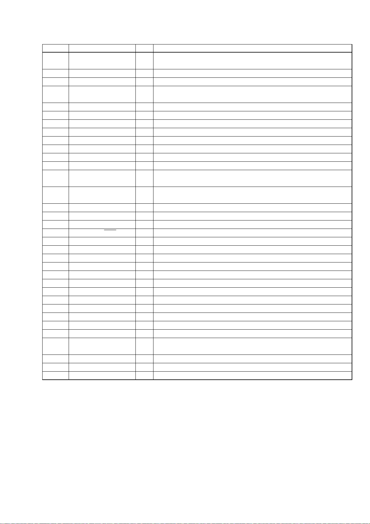
AVD-C700ES
Pin No. Pin Name I/O Pin Description
60 MUTE_2D O
61 SLED I Sled motor servo drive PWM signal input from CD decoder, digital servo processor IC.
62 FG I Spindle motor control signal input
63 SP_ON O
64 JIT I Jitter signal input
65 TE I Tracking error signal input
66 PI I Pull in signal input
67 FE I Focus error signal input
68 AVSS — Ground pin
69 AVREF I Reference voltage input (for A/D converter)
70 AVDD — Power supply pin (+3.3 V) (for A/D converter)
71 GFS_CD I Guard frame sync signal input from CD decoder, digital servo processor IC.
72 SCLK_CD O
73 TSD-M O
74 FOK_CD I Focus OK signal input from CD decoder, digital servo processor IC.
75 LOCK_CD I GFS is sampled by 460 Hz. (H input when GFS is H)
76 LDSEL O Laser diode selection signal output
77 SACD/DVD O SACD/DVD selection signal output
78 I2C_SIO I/O Communication data bus signal input/output
79 I2C_SCL I/O Communication data reading clock signal input/output
80 RXD I Serial data input
81 TXD O Serial data output
82 SDCLK_RF O Serial data transfer clock signal output
83 SDATA_RF I/O Two-way data bus signal input/output
84 XWR O Write strobe signal output to DVD decoder IC.
85 XRD O Read strobe signal output to DVD decoder IC.
86 (PWE) — Not used (Fixed at H)
87 VDD — Power supply pin (+3.3 V)
88 VSS — Ground pin
89 to 96 A0 to A7 O Address signal output to DVD decoder IC.
97 A8 O
98 XDRST O Reset signal output to CD decoder, digital servo processor IC.
99 EEP_CS O Write protect signal output to EEPROM IC.
100 EEP_CLK O Clock signal output to EEPROM IC.
Muting ON/OFF control signal output to focus/tracking coil driver, spindle/sled motor
driver IC.
Muting ON/OFF control signal output to focus/tracking coil driver, spindle/sled motor
driver IC.
SENSE serial data reading clock signal output to CD decoder, digital servo processor
IC.
Thermal shut down signal output to focus/tracking coil driver, spindle/sled motor
driver IC.
Power save control signal output to focus/tracking coil driver, spindle/sled motor
driver IC.
45

AVD-C700ES
• IC1041 ZIVA-5P-C2F (DVD SYSTEM PROCESSOR) (MB Board (9/12))
Pin No. Pin Name I/O Pin Description
1 VDDP — Power supply pin (+3.3 V) (I/O signal)
2 HA1 I/O Address bus signal input/output
3 to 11 HAD15 to HAD7 I/O Data bus (address signal multiplexed) signal input/output
12 VDDP — Power supply pin (+3.3 V) (I/O signal)
13 GNDP — Ground pin (I/O signal)
14 to 19 HAD6 to HAD1 I/O Data bus (address signal multiplexed) signal input/output
20 VDDP — Power supply pin (+3.3 V) (I/O signal)
21 GNDP — Ground pin (I/O signal)
22 HAD0 I/O Data bus (address signal multiplexed) signal input/output
23 HDTACK I/O Acknowledge signal input/output for host data transfer
24 HIRQ0 I Interrupt signal input
25 WEH.UDS I/O Host upper data strobe signal input/output
26 WEL.LDS I/O Host lower data strobe signal output
27 HREAD I/O Read/write strobe signal input/output
28 GPIO0(1)/JIGMODE I/O Jig detection port
29 GND — Ground pin (inside core)
30 VDD — Power supply pin (+1.8 V) (inside core)
31 GND25 — Ground pin (SDRAM I/O signal)
32 VDD25 — Power supply pin (+3.3 V) (SDRAM I/O signal)
33 to 42 MA9 to MA0 O SDRAM address bus signal output to 128 Mbit SD-RAM IC.
43 GND25 — Ground pin (SDRAM I/O signal)
44 VDD25 — Power supply pin (+3.3 V) (SDRAM I/O signal)
45, 46 MA10, MA11 O SDRAM address bus signal output to 128 Mbit SD-RAM IC.
47, 48 BA1, BA0 O SDRAM bank select signal output to 128 Mbit SD-RAM IC.
49 MCS0 O SDRAM chip select signal output to 128 Mbit SD-RAM IC.
50 MCS1 O Not used. (Open)
51 MRAS O SDRAM row address strobe signal output to 128 Mbit SD-RAM IC.
52 MCAS O SDRAM column address strobe signal output to 128 Mbit SD-RAM IC.
53 MWE O SDRAM write enable signal output to 128 Mbit SD-RAM IC. (H: read, L: write)
54 GND25 — Ground pin (SDRAM I/O signal)
55 VDD25 — Power supply pin (+3.3 V) (SDRAM I/O signal)
56 MCLK O SDRAM clock signal output to 128 Mbit SD-RAM IC.
57 to 60 MD0 to MD3 I/O SDRAM data input from/output to 128 Mbit SD-RAM IC.
61 GND25 — Ground pin (SDRAM I/O signal)
62 MDQM0 O Byte read/write mask signal output to 128 Mbit SD-RAM IC.
63 VDD25 — Power supply pin (+3.3 V) (SDRAM I/O signal)
64 to 71 MD4 to MD11 I/O SDRAM data input from/output to 128 Mbit SD-RAM IC.
72 GND25 — Ground pin (SDRAM I/O signal)
73 MDQM1 O Byte read/write mask signal output to 128 Mbit SD-RAM IC.
74 VDD25 — Power supply pin (+3.3 V) (SDRAM I/O signal)
75 to 78 MD12 to MD15 I/O SDRAM data input from/output to 128 Mbit SD-RAM IC.
79 GND — Ground pin (inside core)
80 VDD — Power supply pin (+1.8 V) (inside core)
81 to 84 MD16 to MD19 I/O SDRAM data input from/output to 128 Mbit SD-RAM IC.
85 GND25 — Ground pin (SDRAM I/O signal)
86 MDQM2 O Byte read/write mask signal output to 128 Mbit SD-RAM IC.
87 VDD25 — Power supply pin (+3.3 V) (SDRAM I/O signal)
88 to 95 MD20 to MD27 I/O SDRAM data input from/output to 128 Mbit SD-RAM IC.
96 GND25 — Ground pin (SDRAM I/O signal)
97 MDQM3 O Byte read/write mask signal output to 128 Mbit SD-RAM IC.
98 VDD25 — Power supply pin (+3.3 V) (SDRAM I/O signal)
99 to 102 MD28 to MD31 I/O SDRAM data input from/output to 128 Mbit SD-RAM IC.
46
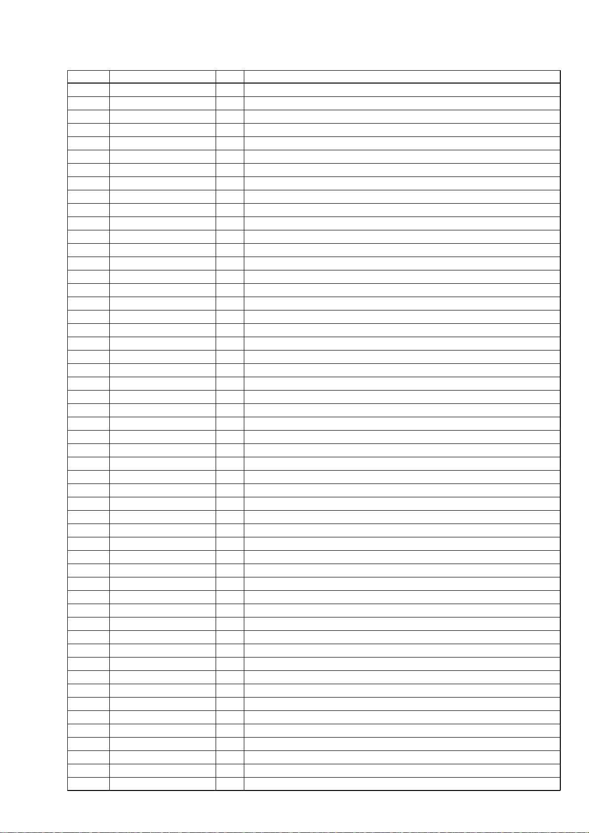
Pin No. Pin Name I/O Pin Description
103 GND25 — Ground pin (SDRAM I/O signal)
104 VDD25 — Power supply pin (+3.3 V) (SDRAM I/O signal)
105 VCLK I/O System clock signal input/output
106 VDATA7 O Video data 7 signal output
107 VDATA6 O Video data 6 signal output
108 VDATA5 O Video data 5 signal output
109 VDATA4 O Video data 4 signal output
110 VDATA3 O Video data 3 signal output
111 VDDP — Power supply pin (+3.3 V) (I/O signal)
112 GNDP — Ground pin (I/O signal)
113 VDATA2 O Video data 2 signal output
114 VDATA1 O Video data 1 signal output
115 VDATA0 O Video data 0 signal output
116 HIRQ2 I Busy signal input from EEPROM IC.
117 VDAC_4B — Video DAC bias bit 4 (Connect to ground)
118 VDAC_VDD4 — Power supply pin (+3.3 V) (Video DAC 4)
119 VDAC_4 O VDAC output 4
120 VDAC_3B — Video DAC bias bit 3 (Connect to ground)
121 VDAC_VDD3 — Power supply pin (+3.3 V) (Video DAC 3)
122 VDAC_3 O VDAC output 3
123 VDAC_2B — Video DAC bias bit 2 (Connect to ground)
124 VDAC_VDD2 — Power supply pin (+3.3 V) (Video DAC 2)
125 VDAC_2 O VDAC output 2
126 VDAC_1B — Video DAC bias bit 1 (Connect to ground)
127 VDAC_VDD1 — Power supply pin (+3.3 V) (Video DAC 1)
128 VDAC_1 O VDAC output 1
129 VDAC_0B — Video DAC bias bit 0 (Connect to ground)
130 VDAC_VDD0 — Power supply pin (+3.3 V) (Video DAC 0)
131 VDAC_0 O VDAC output 0
132 VDAC_DVSS — Ground pin (Video DAC digital system)
133 VDAC_DVDD — Power supply pin (+3.3 V) (Video DAC digital system)
134 VDAC_REFVDD — Power supply pin (+3.3 V) (Video DAC reference)
135 VDAC_REF I Reference voltage input (for Video DAC)
136 VDAC_REFVSS — Ground pin (Video DAC reference)
137 XVSS — Ground pin (crystal oscillator)
138 XOUT O Not used. (Open)
139 XIN I Crystal oscillation signal input
140 XVDD — Power supply pin (+3.3 V) (crystal oscillator)
141 AVSS2 — Ground pin (analog PLL)
142, 143 AVDD2, AVDD1 — Power supply pin (+3.3 V) (analog PLL)
144 AVSS1 — Ground pin (analog PLL)
145 VDD — Power supply pin (+1.8 V) (inside core)
146 GND — Ground pin (inside core)
147 XCK O Audio system clock signal output Not used. (Open)
148 LRCK O LRCK signal output Not used. (Open)
149 BCK O BCK signal output Not used. (Open)
150 GA_RST O GA reset signal output
151 GPIO4 (2) O Video reset signal output to video encoder IC
152 VDDP — Power supply pin (+3.3 V) (I/O signal)
153 GNDP — Ground pin (I/O signal)
154 VS O S1 signal output
155 V-SEL2 O Fixed at L in this set.
156 IEC958 O S/PDIF signal output
AVD-C700ES
47
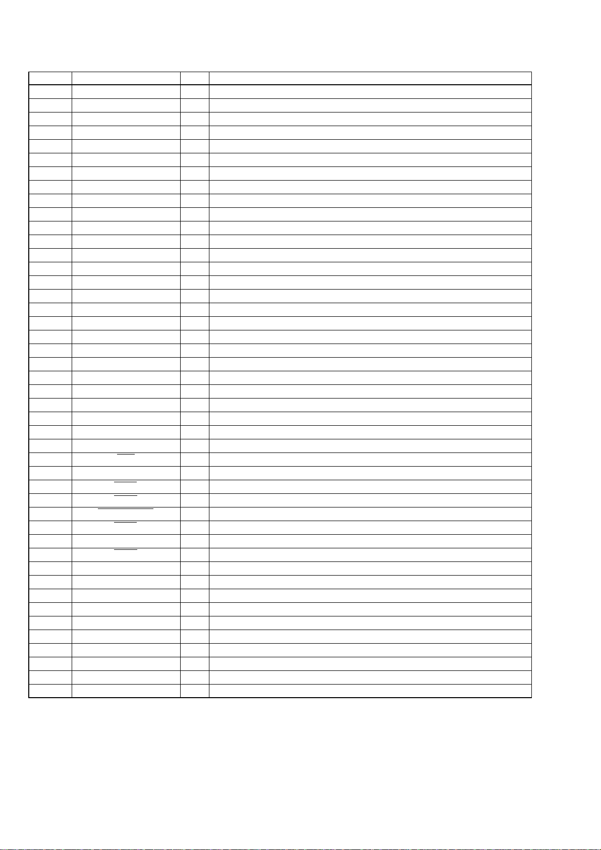
AVD-C700ES
Pin No. Pin Name I/O Pin Description
157 GPIO4 (8) I Not used. (Open)
158 GPIO4 (7) I Not used. (Open)
159 GPIO4 (6) I Not used. (Open)
160 I2C_CL I/O I2C clock bus signal input from/output to mechanism control IC.
161 I2C_DA I/O I2C data bus signal input from/output to mechanism control IC.
162 CS_EEPROM O Chip select signal output to EEPROM IC.
163 RXD1 I Serial data input from check jig
164 TXD1 O Serial data output to check jig
165 WC_EEPROM O Write control signal output to EEPROM IC.
166 GNDP — Ground pin (I/O signal)
167 VDDP — Power supply pin (+3.3 V) (I/O signal)
168 to 171 SDDATA7 to SDDATA4 I SDBUS data input from DVD decoder IC.
172 GND — Ground pin (inside core)
173 VDD — Power supply pin (+1.8 V) (inside core)
174 to 177 SDDATA3 to SDDATA0 I SDBUS data input from DVD decoder IC.
178 SDREQ O SDBUS data request signal output to DVD decoder IC.
179 SDEN I SDBUS data enable signal input from DVD decoder IC.
180 GNDP — Ground pin (I/O signal)
181 VDDP — Power supply pin (+3.3 V) (I/O signal)
182 SDERROR I SDBUS data error signal input from DVD decoder IC.
183 SDCLK I SDBUS data clock signal input from DVD decoder IC.
184 HIRQ1 I Interrupt signal input from mechanism control IC.
185 DRVCLK I Serial data clock signal input from mechanism control IC.
186 DRVTX I Serial data input from mechanism control IC and EEPROM IC.
187 DRVRX O Serial data output to mechanism control IC and EEPROM IC.
188 DRVRDY I Ready signal input from mechanism control IC.
189 VNW — Power supply for 5 V tolerance voltage input
190 ALE O Latch enable signal output for address data demux.
191 RST_SPC O Reset signal output to mechanism control IC.
192 HCS3 O Not used. (Open)
193 HCS2 O Chip select signal output
194 HCS1/XGACS I/O Chip select signal input/output
195 HCS0 O Chip select signal output
196 VDDP — Power supply pin (+3.3 V) (I/O signal)
197 TRST I Reset signal input
198 TDO O Data output
199 TDI I Data input
200 TMS I TMS signal input
201 TCK I TCK signal input
202 RESET I ZIVA reset signal input
203 BUS CLK I/O Not used. (Open)
204 GND — Ground pin (inside core)
205 VDD — Power supply pin (+1.8 V) (inside core)
206, 207 HA3, HA2 I/O Address bus signal input/output
208 GNDP — Ground pin (I/O signal)
48
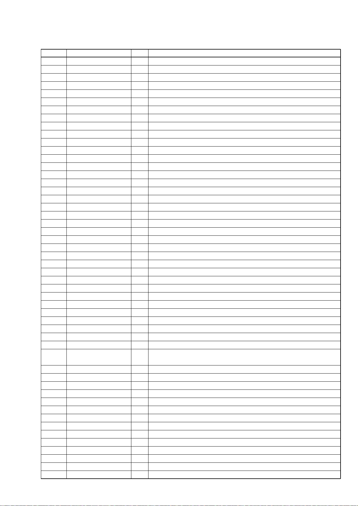
• IC1047 CXD9698R (INTERLACE/PROGRESSIVE CONVERTER) (MB Board (11/12))
Pin No. Pin Name I/O Pin Description
1DVDD — Power supply pin (+3.3 V)
2CLKI I Digital video clock signal (27 MHz) input
3 PLL_TEST I Input for the test (normally: fixed at L)
4 PLL_EN I PLL enable signal input
5, 6 PI0, PI1 I Digital video signal input Not used. (Fixed at L in this set.)
7 to 14 PI2 to PI9 I Digital video signal input
15 NHSI I Horizontal sync signal input Not used. (Fixed at L in this set.)
16 NVSI I Vertical sync signal input Not used. (Fixed at L in this set.)
17 OVSS — Ground pin (for digital system)
18 IVSS — Ground pin (for digital system)
19 CVSS — Ground pin (for digital system)
20 NVSO O Vertical sync signal output Not used. (Open)
21 NHSI O Horizontal sync signal output Not used. (Open)
22 to 25 PO9 to PO6 O Digital video signal output
26 OVDD — Power supply pin (+3.3 V)
27 OVSS — Ground pin (for digital system)
28 to 31 PO5 to PO2 O Digital video signal output
32, 33 PO1, PO0 O Digital video signal output Not used. (Open)
34 TEST0 I Input for the test (normally: fixed at L)
35 OVSS — Ground pin (for digital system)
36 OVDD — Power supply pin (+3.3 V)
37 CVDD — Power supply pin (+2.5 V)
38, 39 TEST1, TEST2 I Input for the test (normally: fixed at L)
40 CLKO I Clock signal (27 MHz) output
41 to 45 YO9 to YO5 O Y (luminance) digital video signal output
46 OVDD — Power supply pin (+3.3 V)
47 OVSS — Ground pin (for digital system)
48 to 52 YO4 to YO0 O Y (luminance) digital video signal output
53 OVDD — Power supply pin (+3.3 V)
54 CVSS — Ground pin (for digital system)
55 OVSS — Ground pin (for digital system)
56 to 60 CO0 to CO4 O C (chroma) digital video signal output to video encoder IC
61 OVDD — Power supply pin (+3.3 V)
62 OVSS — Ground pin (for digital system)
63 to 67 CO5 to CO9 O C (chroma) digital video signal output to video encoder IC
68 FILM O Film detection flag output Not used. (Open)
69 W3IF I
70 OVSS — Ground pin (for digital system)
71 CVDD — Power supply pin (+2.5 V)
72 IVDD — Power supply pin (+3.3 V)
73 OVDD — Power supply pin (+3.3 V)
74 to 77 MD19 to MD16 I/O Two-way data bus terminal Not used. (Open)
78 OVDD — Power supply pin (+3.3 V)
79 OVSS — Ground pin (for digital system)
80 to 83 MA2 to MA5 O Address signal output to SD-RAM IC
84 OVDD — Power supply pin (+3.3 V)
85 OVSS — Ground pin (for digital system)
86 to 89 MA0, MA1, MA6, MA7 O Address signal output to SD-RAM IC
90 OVSS — Ground pin (for digital system)
91 IVSS — Ground pin (for digital system)
92 CVSS — Ground pin (for digital system)
MPU interface communication protocol selection signal input
Not used. (Fixed at L in this set.)
AVD-C700ES
49
AVD-C700ES
Pin No. Pin Name I/O Pin Description
93 OVDD — Power supply pin (+3.3 V)
94 to 97 MA8 to MA11 O Address signal output to SD-RAM IC
98 OVDD — Power supply pin (+3.3 V)
99 OVSS — Ground pin (for digital system)
100 RAS O Row address strobe signal output to SD-RAM IC
101 CKE O Clock enable signal output Not used. (Open)
102 CAS O Column address strobe signal output to SD-RAM IC
103 MCLK O Clock signal (54 MHz) output to SD-RAM IC
104 WE O Write enable signal output to SD-RAM IC
105, 106 TEST3, TEST4 I Input for the test (normally: fixed at L)
107 OVSS — Ground pin (for digital system)
108 OVDD — Power supply pin (+3.3 V)
109 CVDD — Power supply pin (+2.5 V)
110 to 113 MD7 to MD9 I/O Two-way data bus with SD-RAM IC
114 OVDD — Power supply pin (+3.3 V)
115 OVSS — Ground pin (for digital system)
116 to 119 MD4, MD5, MD10, MD11 I/O Two-way data bus with SD-RAM IC
120 OVDD — Power supply pin (+3.3 V)
121 OVSS — Ground pin (for digital system)
122 to 125 MD2, MD3, MD12, MD13 I/O Two-way data bus with SD-RAM IC
126 OVSS — Ground pin (for digital system)
127 CVSS — Ground pin (for digital system)
128 OVDD — Power supply pin (+3.3 V)
129 to 132 MD0, MD1, MD14, MD15 I/O Two-way data bus with SD-RAM IC
133 SLV I MPU interface slave address selection signal input Not used. (Fixed at L in this set.)
134 CSB I MPU interface chip select signal input Not used. (Fixed at L in this set.)
135 SDA I/O Two-way data bus input/output
136 SCL I Clock signal input
137 SRN I Reset signal input from the system controller “L”: reset
138 OVSS — Ground pin (for digital system)
139 CVDD — Power supply pin (+2.5 V)
140 PLL_VDD — Power supply pin (+2.5 V) (for PLL)
141 CPOUT O PLL charge pump output
142 VCOIN I PLL external loop filter input
143 PLL_GND — Ground pin (for PLL)
144 IVDD — Power supply pin (+3.3 V)
50
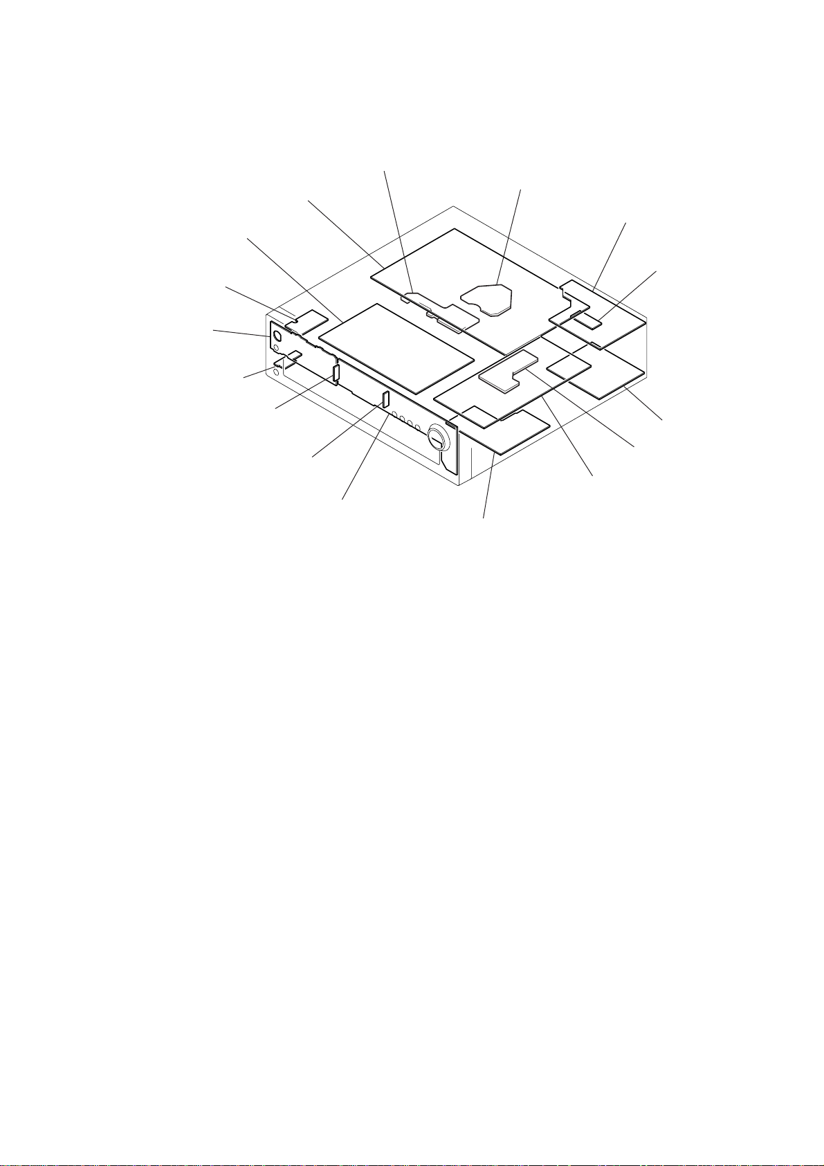
6-2. CIRCUIT BOARDS LOCATION
d
AMP board
POWER board
AC SW board
RM board
HEADPHONE board
AVD-C700ES
SE-130 board
RF board
VIDEO I/O board
COMPONENT boar
BACK LIGHT (L) board
BACK LIGHT (R) board
AUDIO I/O board
MD-94 board
MB board
DISPLAY board
LINK board
51
AVD-C700ES
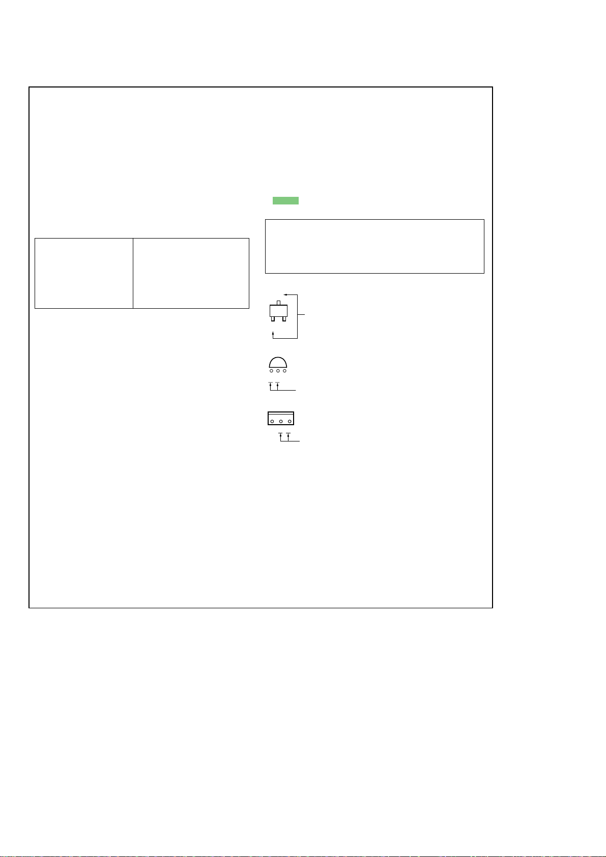
6-3. NOTE FOR PRINTED WIRING BOARDS AND SCHEMATIC DIAGRAMS
THIS NOTE IS COMMON FOR PRINTED WIRING
BOARDS AND SCHEMATIC DIAGRAMS.
(In addition to this, the necessary note is printed
in each block.)
For schematic diagrams.
Note:
• All capacitors are in µF unless otherwise noted. pF: µµF
50 WV or less are not indicated except for electrolytics
and tantalums.
• All resistors are in Ω and 1/
specified.
f
•
• C : panel designation.
Note:
The components identified by mark 0 or dotted
line with mark 0 are criti-
cal for safety.
Replace only with part
number specified.
• A : B+ Line.
• B : B– Line.
• H : adjustment for repair .
•Voltages and waveforms are dc with respect to ground
no mark : DVD PLAY
: internal component.
under no-signal (detuned) conditions.
(): CD PLAY
[]: SACD PLAY
4
W or less unless otherwise
Note:
Les composants identifiés par
une marque 0 sont critiques
pour la sécurité.
Ne les remplacer que par une
piéce portant le numéro
spécifié.
∗ : Impossible to measure
•Voltages are taken with a VOM (Input impedance 10 MΩ).
Voltage variations may be noted due to normal production tolerances.
•Waveforms are taken with a oscilloscope.
Voltage variations may be noted due to normal production tolerances.
• Circled numbers refer to waveforms.
• Signal path.
J : CD PLAY
c : DVD PLAY
I : SACD PLAY
f : AUX IN
i : OPTICAL DIGITAL IN
d : TUNER
F : AUDIO
L : VIDEO
E : Y
a : CHROMA
r : COMPONENT VIDEO
• Abbreviation
CND : Canadian model.
For printed wiring boards.
Note:
• X : parts extracted from the component side.
• Y : parts extracted from the conductor side.
a
•
• : Pattern from the side which enables seeing.
(The other layers' patterns are not indicated.)
Caution:
Pattern face side: Parts on the pattern face side seen from the
(Side B) pattern face are indicated.
Parts face side: Parts on the parts face side seen from the
(Side A) parts face are indicated.
• Abbreviation
: Through hole.
C
Q
These are omitted
EB
E
CB
These are omitted
C
BE
These are omitted
CND : Canadian model.
52
 Loading...