

SONY AN498 Service Manual
Prepared
Checked
Approved
Tentative
Product Specifications
AN17820B
Ref No.
Total Page
Page No.
A-1
9
1
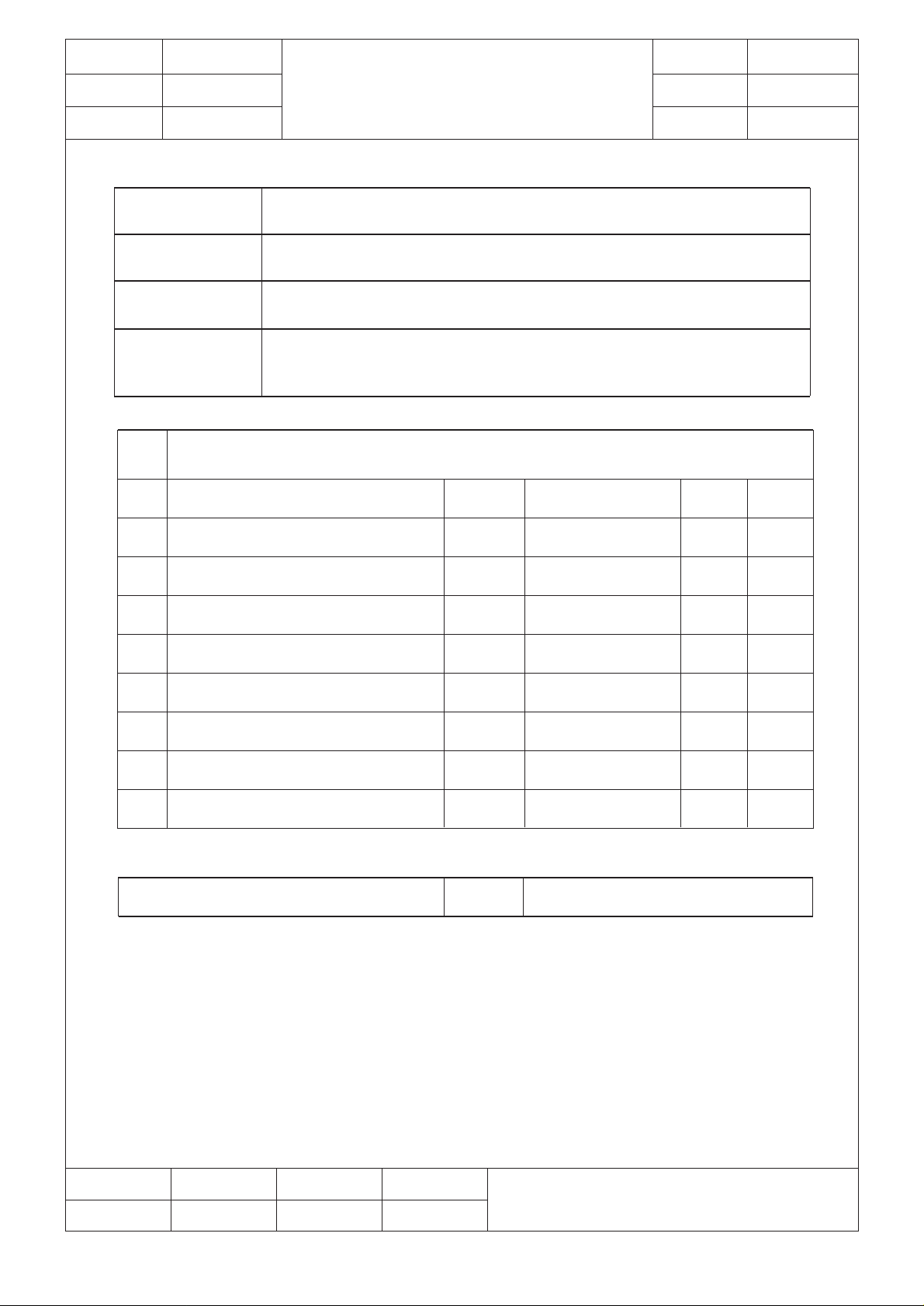
Structure
Appearance
Application
Function
Absolute Maximum RatingsA
No. Item
1
Storage Temperature
2
Operating Ambient Temperature
3
Operating Ambient Pressure
4
Operating Constant Acceleration
Silicon Monolithic Bipolar IC
SIL-12 Pin Plastic Package (Power Type with Fin)
Low Frequency Amplifier
BTL 7.5W x 2ch Power Amplifier
with Standby Function and Volume Function
Symbol
Tstg
Topr
Popr
Gopr
Ratings
-55 ~ +150
-25 ~ +70
1.013x10⁵±0.61x10
9,810
Unit
5
m/s
° C
° C
Pa
Note
1
1
2
5
Operating Shock
6
Supply Voltage
7
Supply Current
8
Power Dissipation
Operating Supply Voltage Range
Note 1)
The temperature of all items shall be Ta=25°C except storage temperature and
operating ambient temperature.
2)
At no signal input.
Sopr
Vcc
Icc
P
D
Vcc 5V ~ 18V
4,900
24
4.0
37.5
m/s
V
A
W
2
2
Ta=70°C
Eff. Date Eff. Date Eff. Date Eff. Date
09-JUL-2001
Semiconductor Company , Matsushita Electric Industrial Co., Ltd.FMSC-PSDA-002-01 Rev.1
Prepared
Checked
Approved
Tentative
Product Specifications
AN17820B
Ref No.
Total Page
Page No.
B-1
9
2
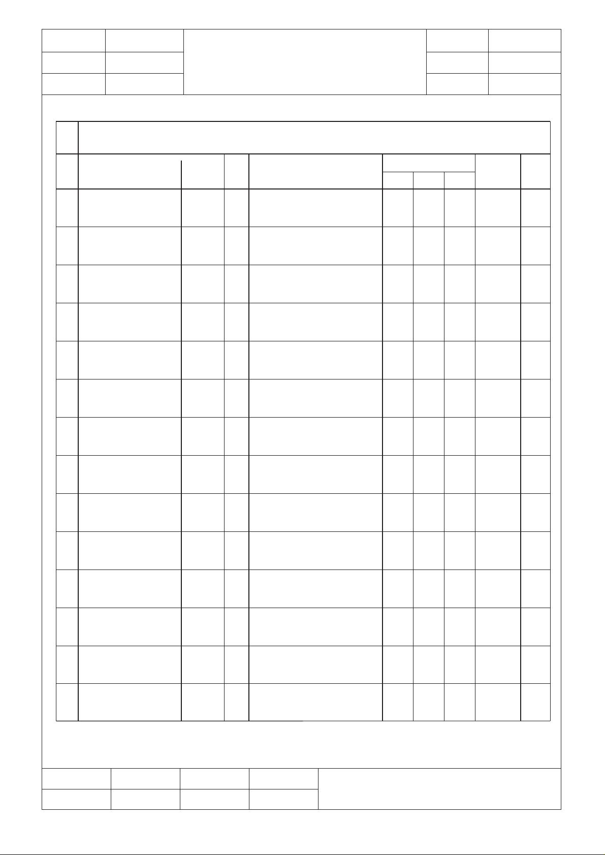
Electrical CharacteristicsB
No Item
Quiescent Circuit
1
Current
Standby Current
2
Output Noise
3
Voltage
Voltage Gain
4
Total Harmonic
5
Distortion
Maximum Power
6
Output 1
Symbol
I
CQ
I
STB
V
NO
G
V
THD
PO1
(Unless otherwise specified, the ambient temperature is 25°C±2°C,
Vcc=12V, frequency=1kHz and RL=8Ω.)
Test
Cir-
Conditions
cuit
Vin=0V, Vol=0V
1
Vin=0V, Vol=0V
1
Rg=10kΩ, Vol=0V
1
Po=1.0W, Vol=1.25V
1
1
Po=1.0W, Vol=1.25V
THD=10%, Vol=1.25V
1
-
-
-
38
-
6.0
Limits
45
1
0.2
40
0.10
7.5
maxtypmin
100
10
0.6
42
0.5
mVrms
-
Unit
mA
Note
µA
1
dB
%
W
Maximum Power
7
Output 2
Ripple Rejection
8
Ratio
Output Offset
9
Voltage
Volume
10
Attenuation Ratio
11
Channel Balance 1
12
Channel Balance 2
Middle Voltage
13
Gain
14
Channel Crosstalk
PO2
RR
Voff
Att
CB1
CB2
G
Vm
CT
Vcc=15V
1
THD=10%, Vol=1.25V
Rg=10kΩ, Vol=0V
1
Vr=1Vrms, fr=120Hz
Rg=10kΩ, Vol=0V
1
Po=1.0W, Vol=0V
1
Po=1.0W, Vol=1.25V
1
1
Po=1.0W, Vol=0.6V
Po=1.0W, Vol=0.6V
1
Po=1.0W, Vol=1.25V
1
10.0
30
-350
70
-1
-2
26.5
40
12.5
50
0
80
0
0
29.5
55
-
-
350
-
1
2
32.5
-
W
dB
mV
dB
dB
dB
dB
dB
1
1
Note 1) For this measurement, use the BPF = 15Hz ~ 30kHz (12dB/OCT).
Eff. Date Eff. Date Eff. Date Eff. Date
09-JUL-2001
Semiconductor Company , Matsushita Electric Industrial Co., Ltd.FMSC-PSDA-002-01 Rev.1
Prepared
Checked
Approved
Tentative
Product Specifications
AN17820B
Ref No.
Total Page
Page No.
B-2
9
3
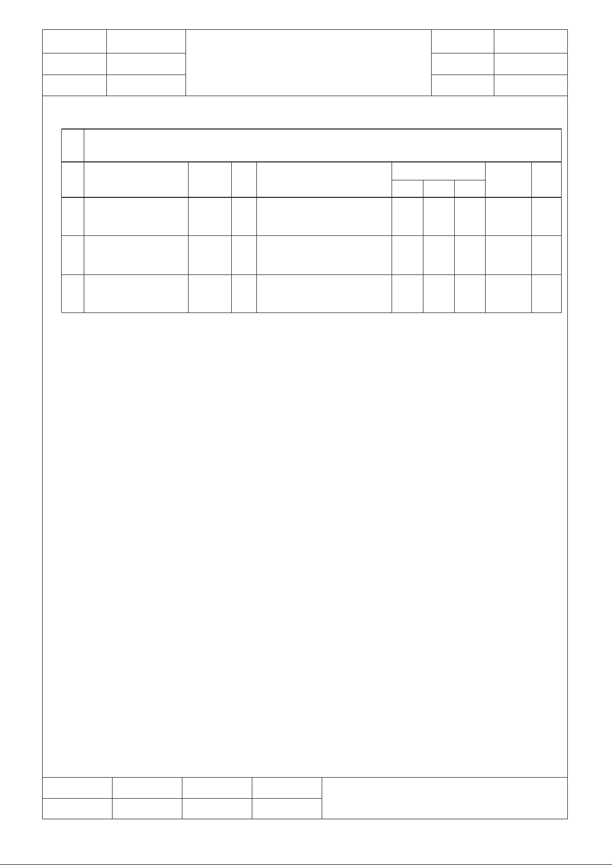
Electrical CharacteristicsB
No Item
Standby pin
1
current
Volume pin
2
current
Input Impedance
3
Note)
The above characteristics are reference values determined for IC design, but not guaranteed
values for shipping inspection. If problems were to occur, counter measures will be
sincerely discussed.
Symbol
I
STB2
I
VOL
Z
i
(Unless otherwise specified, the ambient temperature is 25°C±2°C,
Vcc=12V, frequency=1kHz and RL=8Ω.)
Test
Cir-
Conditions
cuit
Vin=0V, VSTB=3V
1
Vin=0V, Vol=0V
1
Vin=±0.3VDC
1
-
-12
24
Limits
-
-
30
maxtypmin
25
-
36
Unit
kΩ
Note
µA
µA
Eff. Date Eff. Date Eff. Date Eff. Date
09-JUL-2001
Semiconductor Company , Matsushita Electric Industrial Co., Ltd.FMSC-PSDA-002-01 Rev.1
 Loading...