

Sony AA-2W, KV-29FV16A Service Manual
SERVICE MANUAL
MODEL NAME REMOTE COMMANDER DESTINATION CHASSIS NO.
AA-2W
CHASSIS
KV-29FV16A
RM-Y171 Argentina SCC-S34P-A
9-965-908-01
KV-29FV16A
RM-Y171
TRINITRON® COLOR TELEVISION

TABLE OF CONTENTS
SECTION TITLE PAGE
Specifi cations..................................................................................................................................... 3
Warnings and Cautions...................................................................................................................... 4
Safety Check-out ............................................................................................................................... 5
1. Disassembly
1-1. Rear Cover Removal ................................................................................................................. 6
1-2. Chassis Assembly Removal ...................................................................................................... 6
1-3. Service Position......................................................................................................................... 6
1-4. Multi-Button Switch Removal..................................................................................................... 6
1-5. Picture Tube Removal ............................................................................................................... 7
Anode Cap Removal Procedure ........................................................................................................ 7
2. Set-up Adjustments
2-1. Beam Landing ............................................................................................................................ 8
2-2. Convergence .............................................................................................................................. 9
2-3. Focus.........................................................................................................................................11
2-4. Screen (G2) ...............................................................................................................................11
2-5. White Balance Adjustments.......................................................................................................11
KV-29FV16A
3. Safety Related Adjustments
3-1. Hold Down Confi rmation........................................................................................................... 12
3-2. B+ Voltage Confi rmation and Adjustment................................................................................. 12
4. Circuit Adjustments
4-1. Setting the Service Adjustment Mode......................................................................................13
4-2. Memory Write Confi rmation Method ........................................................................................ 13
4-3. Remote Adjustment Buttons and Indicators............................................................................. 13
4-4. A Board Adjustments ............................................................................................................... 19
5. Diagrams
5-1. Circuit Board Location ............................................................................................................. 21
5-2. Printed Wiring Boards and Schematic Diagrams..................................................................... 21
5-3. Diagrams
Block Diagram ......................................................................................................................... 22
A Board.................................................................................................................................... 24
AK Board ................................................................................................................................. 27
C Board.................................................................................................................................... 29
HB Board ................................................................................................................................. 30
HZ Board ................................................................................................................................. 30
HA Board ................................................................................................................................. 31
HX Board ................................................................................................................................. 31
GA Board ................................................................................................................................. 32
UY Main Board ........................................................................................................................ 35
UY PIP Board........................................................................................................................... 36
WA Board................................................................................................................................. 40
5-4. Semiconductors ....................................................................................................................... 42
6. Exploded Views
6-1. Chassis..................................................................................................................................... 43
6-2. Picture Tube Removal .............................................................................................................. 44
7. Electrical Parts List .................................................................................................................................. 45
— 2 —
SPECIFICATIONS
KV-29FV16A
KV-29FV16A
Television system
NTSC/PAL-M/PAL-N Color System
Channel coverage
VHF: 2-13/ VHF: 14-69/ CATV: 1-125
Picture tube
Flat Trinitron® tube
Power Requirements
120-220V, 50/60Hz
Number of Inputs/Outputs
Video
S Video
Y,PB, PR
Audio
Audio Out
Monitor Out
S-Link
Speaker Output (W)
Power Consumption (W)
In Use (Max)
In Standby
1)
3
2)
2
3)
1
4)
3
5)
1
1
YES
15W x 2
205W
1W
Dimensions (W x H x D)
mm
762 x 604 x 519 mm
in
30 x 23
Mass
kg
49 kg
lbs
110 lbs
1) 1 Vp-p 75 ohms unbalanced, sync negative
2) Y: 1 Vp-p 75 ohms unbalanced, sync negative
C: 0.286 Vp-p (Burst signal), 75 ohms
3) Y: 1.0 Vp-p, 75 ohms, sync negative;
PB: 0.7 Vp-p, 75 ohms; PR: Vp-p, 75 ohms
m
Vrms (100% modulation), Impedance: 47 kilohms
4) 500
5) More than 408 mVrms at the maximum volume setting (variable)
More than 408 mVrms (fi x); Impedance (output): 2 kilohms
7/8
x 20
1/2
in
Visible screen size
27-inch picture measured diagonally
Actual screen size
29-inch measured diagonally
Antenna
75 ohm external terminal for VHF/UHF
Supplied Accessories
Remote Control RM-Y171
Battery size AA (R6) w/2
Optional Assessories
Connecting Cables:
RK-74A, VMC-810/820830hg, VMC-10HG/30HG,
VMC-720M, VMC-810S/820S, YC-15V/30V,
YC-15/30HG, RK-G69HG, RKC-515HG
AV Cable: VMC-810/820/830 HG
Audio Cable: RKC-515HG
S-LINK Cable: RK-G69HG
Component Video Cable: VMC-10/30 HG
TV Stand: SU-32FD2, SU-36FD2, SU-32XBR2, SU-36XBR2
UV Mixer: EAC-66
Design and specifi cations are subject to change without notice.
(•) SRS (SOUND RETRIEVAL SYSTEM)
The (•) SRS (SOUND RETRIEVAL SYSTEM) is manufactured by Sony
Corporation under license from SRS Labs, Inc. It is covered by U.S.
Patent No. 4,748,669. Other U.S. and foreign patents pending.
The word ‘SRS’ and the SRS symbol (•) are registered trademarks of
SRS Labs, Inc. BBE and BBE symbol are trademarks of BBE Sound, Inc.
and are licensed by BBE Sound, Inc. under U.S. Patent No. 4,638,258
and 4,482,866.
— 3 —

WARNINGS AND CAUTIONS
CAUTION
Short circuit the anode of the picture tube and the anode cap to the metal chassis, crt shield, or carbon painted on the crt, after
removing the anode.
WARNING!!
An isolation transformer should be used during any service to avoid possible shock hazard, because of live chassis. The chassis of
this receiver is directly connected to the ac power line.
! SAFETY-RELATED COMPONENT WARNING!!
KV-29FV16A
Components identifi ed by shading and ! mark on the schematic diagrams, exploded views, and in the parts list are critical for
safe operation. Replace these components with sony parts whose part numbers appear as shown in this manual or in supplements
published by sony. Circuit adjustments that are critical for safe operation are identifi ed in this manual. Follow these procedures
whenever critical components are replaced or improper operation is suspected.
ATTENTION!!
Apres avoir deconnecte le cap de l’anode, court-circuiter l’anode du tube cathodique et celui de l’anode du cap au chassis metallique
de l’appareil, ou la couche de carbone peinte sur le tube cathodique ou au blindage du tube cathodique.
Afi n d’eviter tout risque d’electrocution provenant d’un chássis sous tension, un transformateur d’isolement doit etre utilisé lors de tout
dépannage. Le chássis de ce récepteur est directement raccordé à l’alimentation du secteur.
! ATTENTION AUX COMPOSANTS RELATIFS A LA SECURITE!!
Les composants identifi es par une trame et par une marque ! sur les schemas de principe, les vues explosees et les listes de
pieces sont d’une importance critique pour la securite du fonctionnement. Ne les remplacer que par des composants sony dont
le numero de piece est indique dans le present manuel ou dans des supplements publies par sony. Les reglages de circuit dont
l’importance est critique pour la securite du fonctionnement sont identifi es dans le present manuel. Suivre ces procedures lors de
chaque remplacement de composants critiques, ou lorsqu’un mauvais fonctionnement suspecte.
— 4 —
SAFETY CHECK-OUT
KV-29FV16A
After correcting the original service problem, perform the following
safety checks before releasing the set to the customer:
1. Check the area of your repair for unsoldered or poorly soldered
connections. Check the entire board surface for solder splashes and
bridges.
2. Check the interboard wiring to ensure that no wires are “pinched” or
touching high-wattage resistors.
3. Check that all control knobs, shields, covers, ground straps, and
mounting hardware have been replaced. Be absolutely certain that
you have replaced all the insulators.
4. Look for unauthorized replacement parts, particularly transistors,
that were installed during a previous repair. Point them out to the
customer and recommend their replacement.
5. Look for parts which, though functioning, show obvious signs of
deterioration. Point them out to the customer and recommend their
replacement.
6. Check the line cords for cracks and abrasion. Recommend the
replacement of any such line cord to the customer.
7. Check the B+ and HV to see if they are specifi ed values. Make sure
your instruments are accurate; be suspicious of your HV meter if sets
always have low HV.
8. Check the antenna terminals, metal trim, “metallized” knobs, screws,
and all other exposed metal parts for AC leakage. Check leakage
as described below.
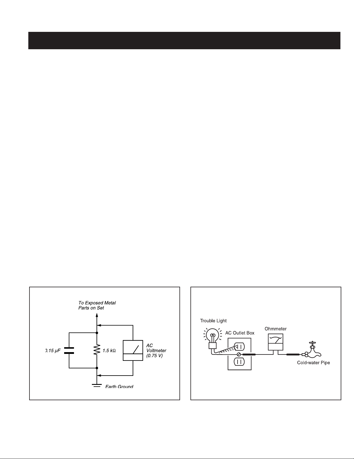
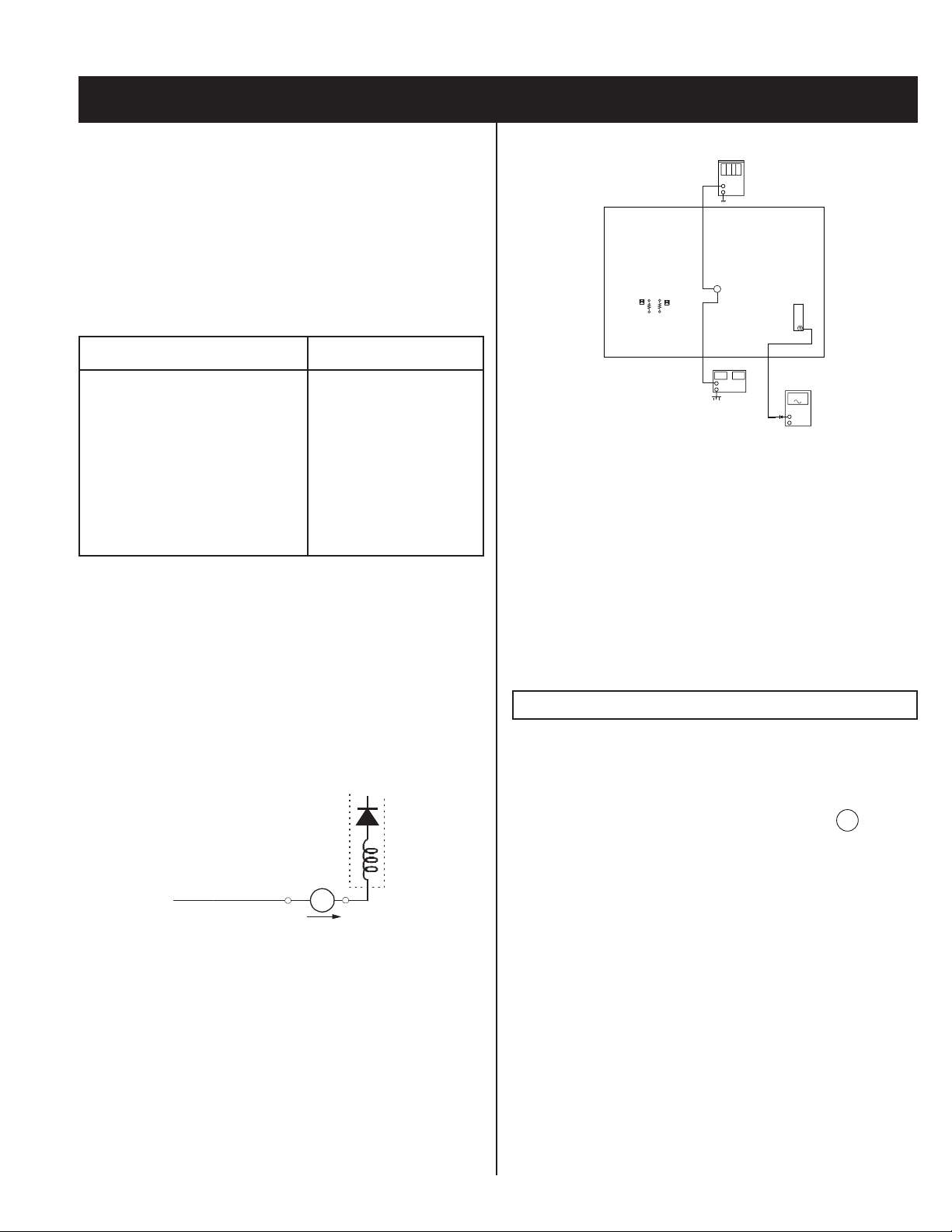
Leakage Test
The AC leakage from any exposed metal part to earth ground and from
all exposed metal parts to any exposed metal part having a return to
chassis, must not exceed 0.5 mA (500 microamperes). Leakage current
can be measured by any one of three methods.
1. A commercial leakage tester, such as the Simpson 229 or
RCA WT-540A. Follow the manufacturers’ instructions to use these
instructions.
2. A battery-operated AC milliammeter. The Data Precision 245 digital
multimeter is suitable for this job.
3. Measuring the voltage drop across a resistor by means of a VOM
or battery-operated AC voltmeter. The “limit” indication is 0.75 V,
so analog meters must have an accurate low voltage scale. The
Simpson’s 250 and Sanwa SH-63TRD are examples of passive
VOMs that are suitable. Nearly all battery-operated digital multimeters
that have a 2 VAC range are suitable (see Figure A).
How to Find a Good Earth Ground
A cold-water pipe is a guaranteed earth ground; the cover-plate retaining
screw on most AC outlet boxes is also at earth ground. If the retaining
screw is to be used as your earth ground, verify that it is at ground
by measuring the resistance between it and a cold-water pipe with an
ohmmeter. The reading should be zero ohms.
If a cold-water pipe is not accessible, connect a 60- to 100-watt troublelight (not a neon lamp) between the hot side of the receptacle and the
retaining screw. Try both slots, if necessary, to locate the hot side on the
line; the lamp should light at normal brilliance if the screw is at ground
potential (see Figure B).
Figure A. Using an AC voltmeter to check AC leakage. Figure B. Checking for earth ground.
— 5 —
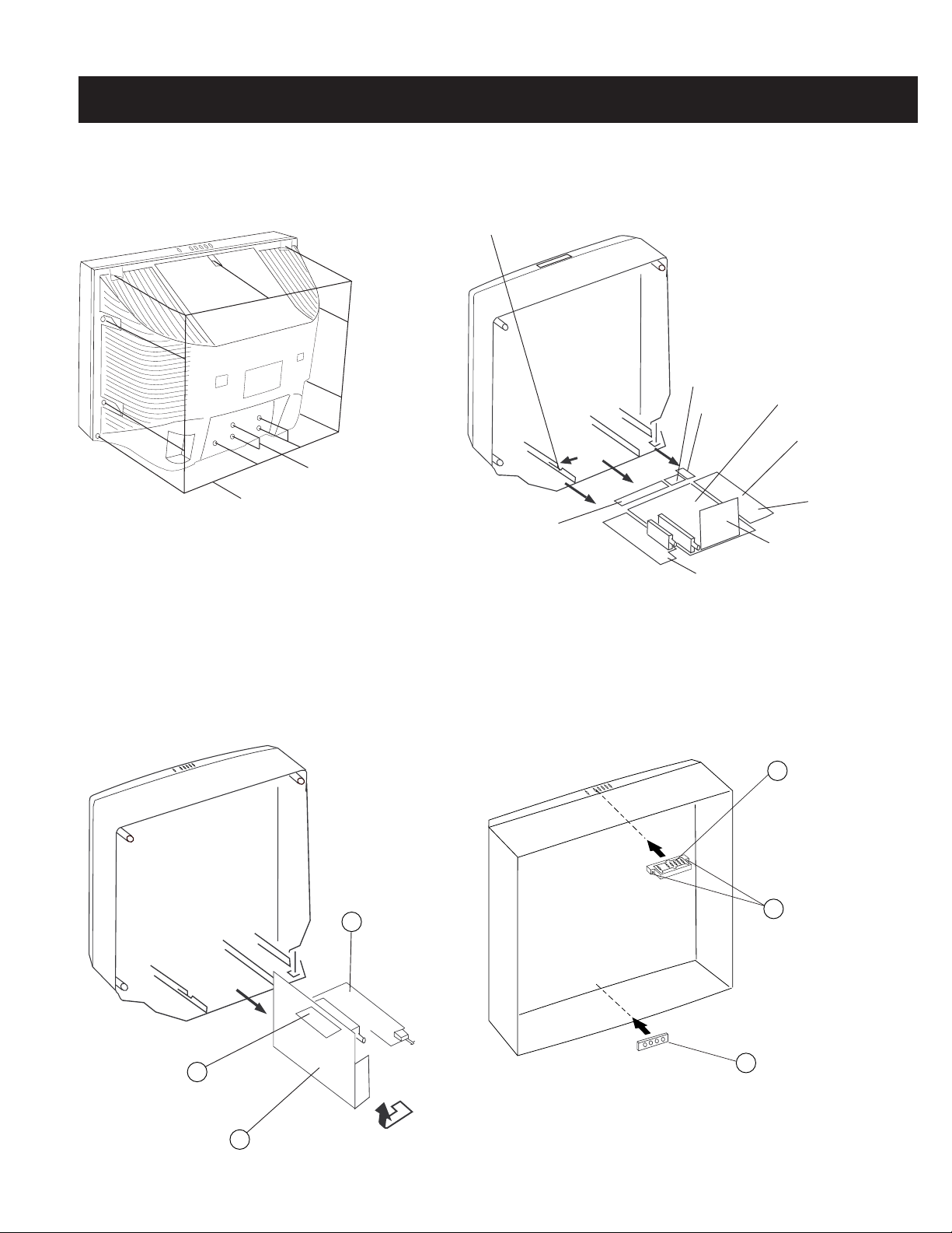
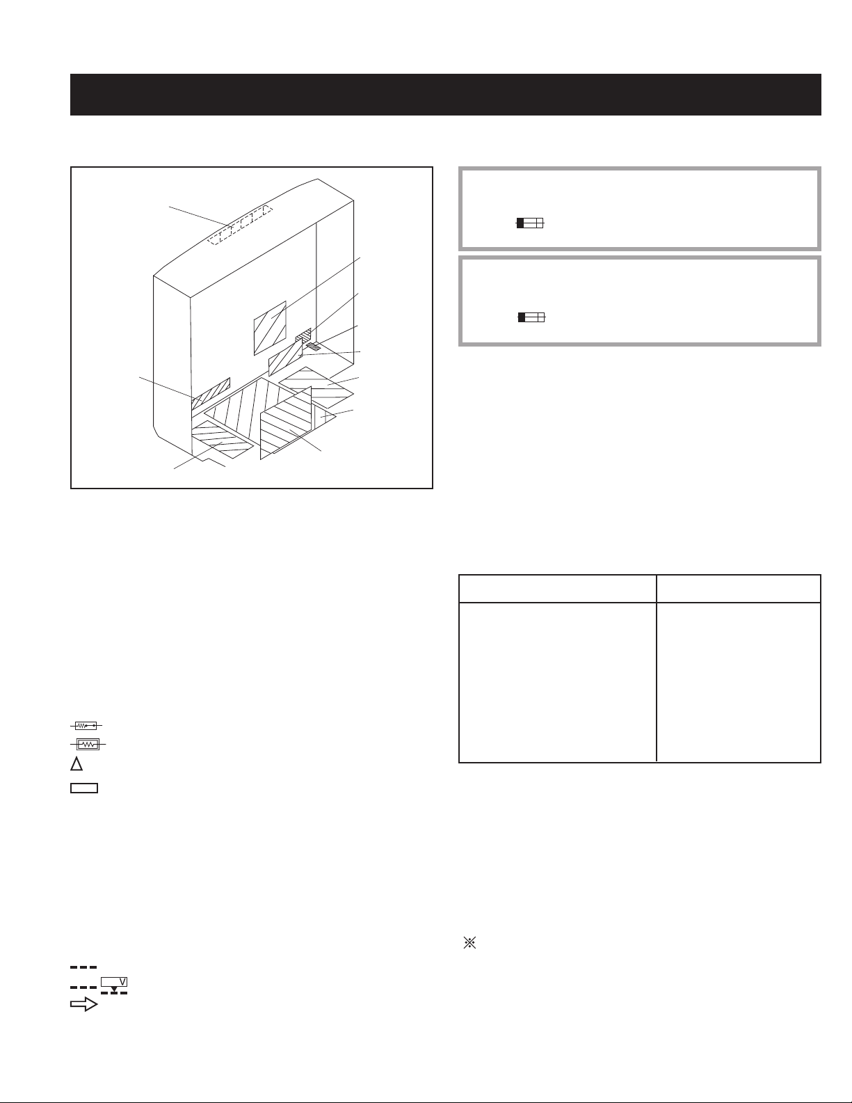
SECTION 1: DISASSEMBLY
1-1. REAR COVER REMOVAL 1-2. CHASSIS ASSEMBLY REMOVAL
Claw
HB Board
A Board
UY Board
Twelve Screws
(BVTP 4 x 16)
HZ Board
Two Screws
(BVTP 3 x 12)
HA Board
KV-29FV16A
GA Board
Chassis Assembly
AK Board
1-3. SERVICE POSITION 1-4. MULTI-BUTTON SWITCH REMOVAL
Top Multi-Button Switch
1
Two Screws
2
3
GA Board
(+BVTP 4x16)
AK Board
2
1
A Board
— 6 —
Bottom Multi-Button Switch
3
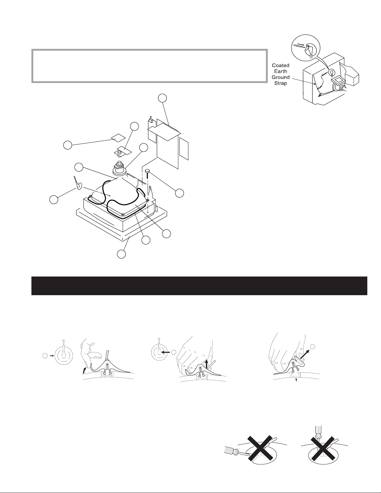
1-5. PICTURE TUBE REMOVAL
WARNING: BEFORE REMOVING THE ANODE CAP
High voltage remains in the CRT even after the power is disconnected. To avoid electric shock,
discharge CRT before attempting to remove the anode cap. Short between anode and CRT
coated earth ground strap.
4
KV-29FV16A
5
3
6
2
10
1
1. Discharge the anode of the CRT and remove the anode cap.
2. Unplug all interconnecting leads from the defl ection yoke, neck
assembly, degaussing coils and CRT grounding strap.
3. Remove the C Board from the CRT.
4. Remove the chassis assembly.
5. Loosen the neck assembly fi xing screw and remove.
6. Loosen the defl ection yoke fi xing screw and remove.
7. Place the set with the CRT face down on a cushion and remove the
degaussing coil holders.
8. Remove the degaussing coils.
9. Remove the CRT grounding strap and spring tension devices.
10. Unscrew the four CRT fi xing screws [located on each CRT corner]
and remove the CRT [Take care not to handle the CRT by the
neck].
9
8
7
ANODE CAP REMOVAL PROCEDURE
WARNING: High voltage remains in the CRT even after the power is disconnected. To avoid electric shock, discharge CRT before attempting to remove
the anode cap. After removing the anode cap, short circuit to either the metal chassis, CRT shield, or carbon painted on the CRT.
REMOVAL PROCEDURES
a
Turn up one side of the rubber cap
inthe direction indicated by arrow a .
b
Use your thumb to pull the rubber
cap fi rmly in the direction indicated
by arrow b .
HOW TO HANDLE AN ANODE CAP
1. Do not use sharp objects which may cause damage to the surface of the anode
cap.
2. To avoid damaging the anode cap, do not squeeze the rubber covering too hard.
A material fi tting called a shatter-hook terminalis built into the rubber.
3. Do not force turn the foot of the rubber cover. This may cause the shatter-hook
terminal to protrude and damage the rubber.
— 7 —
Anode Button
When one side of the rubber cap separates from
the anode button, the anode cap can be removed
by turning the rubber cap and pulling it in the
direction of arrow c .
c
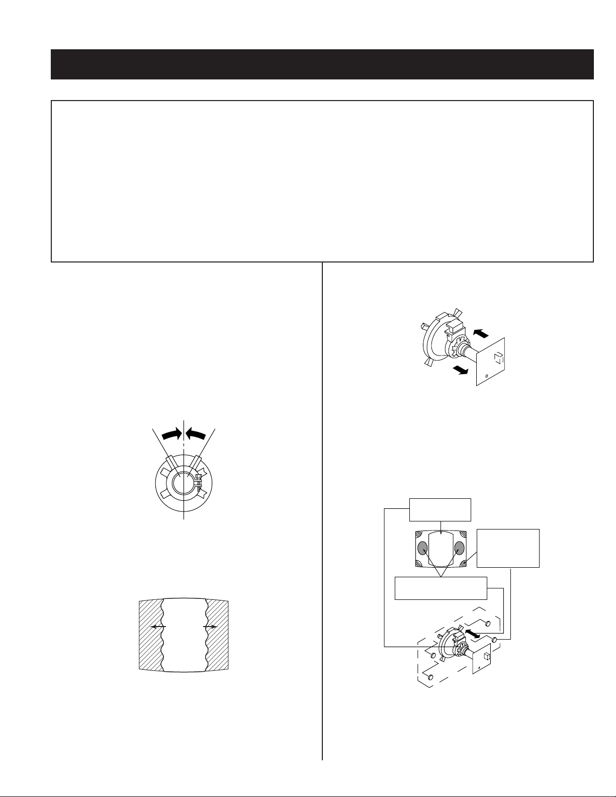
SECTION 2: SET-UP ADJUSTMENTS
KV-29FV16A
The following adjustments should be made when a complete
realignment is required or a new picture tube is installed.
These adjustments should be performed with rated power supply
voltage unless otherwise noted.
The controls and switch should be set as follows unless otherwise
noted:
PICTURE CONTROL: normal
BRIGHTNESS CONTROL: normal
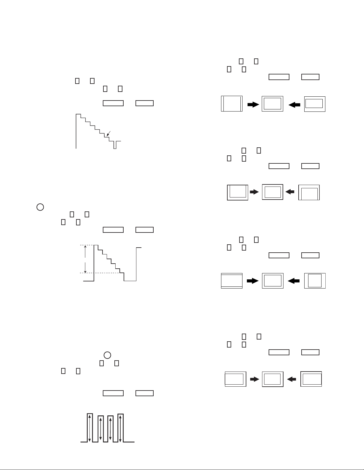
2-1. BEAM LANDING
Preparation:
• Input a white pattern signal.
• Face the picture tube in an East or West direction to reduce the
infl uence of geomagnetism.
NOTE: Do not use the hand degausser; it magnetizes the CRT .
1. Input white pattern from pattern generator.
2. Loosen the defl ection yoke mounting screw, and set the purity control
to the center as shown below:
Perform the adjustments in order as follows:
1. Beam Landing
2. Convergence
3. Focus
4. Screen (G2)/White Balance
Test Equipment Required:
1. Color Bar Pattern Generator
2. Degausser
3. DC Power Supply
4. Digital Multimeter
5. Oscilloscope
6. CRT Analyzer
5. Move the defl ection yoke forward, and adjust so that the entire screen
becomes green.
6. Switch over the raster signal to red and blue and confi rm the
condition.
7. When the position of the defl ection yoke is determined, tighten it with
the defl ection yoke mounting screw.
8. When landing at the corner is not right, adjust by using the disk
magnets.
3. Input green pattern from pattern generator.
4. Move the defl ection yoke backward, and adjust with the purity control
so that green is in the center and red and blue are even on both
sides.
Blue Red
Green
— 8 —
Purity control
corrects this area.
ab
cd
Deflection yoke positioning
corrects these areas.
a
d
Disk magnets or
rotatable disk
magnets correct
these areas(a-d).
b
c
KV-29FV16A
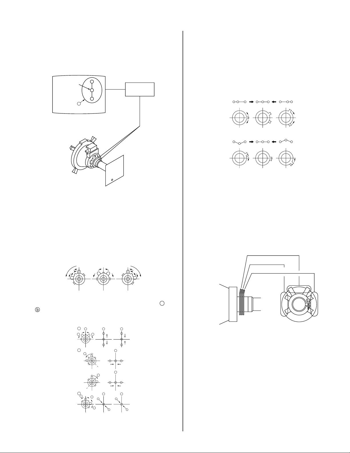
2-2. CONVERGENGE
Preparation:
• Perform FOCUS, V. LIN and V. SIZE adjustments.
• Set BRIGHTNESS control to minimum.
• Input dot pattern.
Center dot
R
G
V.STAT
Magnet
B
VERTICAL AND HORIZONTAL STATIC
CONVERGENCE
1. Adjust V. STAT magnet to converge red, green and blue dots in the
center of the screen (Vertical movement).
Tilt the V. STAT magnet and adjust static convergence to open or
close the V. STAT magnet.
OPERATION OF BMC (HEXAPOLE) MAGNET
The respective dot positions resulting from moving each magnet interact,
so perform adjustment while tracking.
1 Use the V.STAT tabs to adjust the red, green, and blue dots so they
line up at the center of the screen (move the dots in a horizontal
direction).
RG B
RGB RGB
RGB
RGB
RGB
Y SEPARATION AXIS CORRECTION MAGNET
ADJUSTMENT
1. Input cross-hatch pattern, adjust PICTURE to minimum and
BRIGHTNESS to normal.
2. Adjust the defl ection yoke upright so it touches the CRT.
3. Adjust so that the Y separation axis correction magnet on the neck
assembly is symmetrical from top to bottom (open state).
Purity
2. When the V. STAT magnet is moved in the direction of arrow a and
, red, green, and blue dots move as shown below:
1
a
b
2
a
3
b
a
B
b
G
R
b
a
a
R
G
b
a
RG B
b
BG R
B
B
b
B
G
R
b
G
R
V. STAT
BMC (Hexapole)
4. Return the defl ection yoke to its original position.
— 9 —
KV-29FV16A
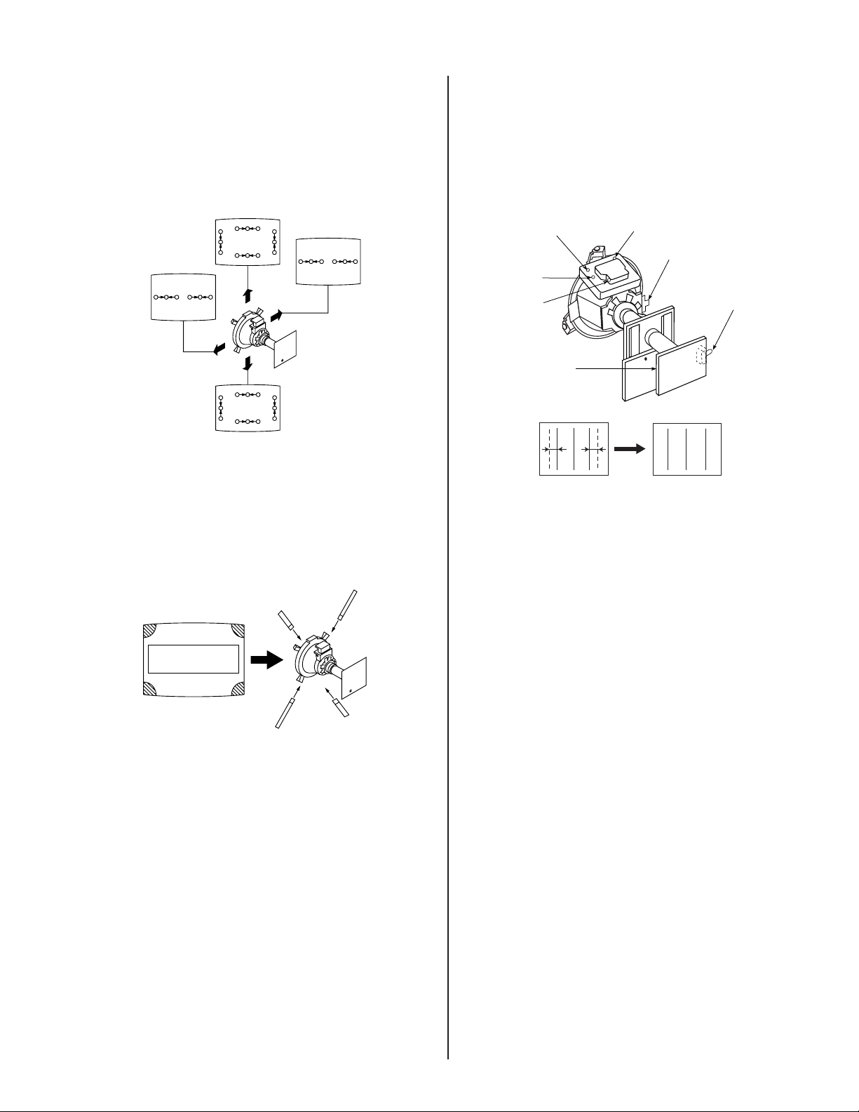
DYNAMIC CONVERGENCE ADJUSTMENT
Before starting, perform Vertical and Horizontal Static Convergence
Adjustment.
1. Slightly loosen defl ection yoke screw.
2. Remove defl ection yoke spacers.
3. Move the defl ection yoke for best convergence as shown below:
R
B
BGR
G
G
RGB
R
B
RGB
BGR
B
RGB
G
BGR
R
4. Tighten the defl ection yoke screw.
5. Install the defl ection yoke spacers.
R
G
B
RGB RGB
TLH PLATE ADJUSTMENT
Preparation:
• Input crosshatch pattern.
• Adjust Picture Quality to standard, Picture and Brightness to 50%, and
Other to standard.
• Adjust the Horizontal Convergence of red and blue dots by tilting the
TLH plate on the defl ection yoke.
YCH
TLV
XCV
C Board
B R R B
(R)(B) (B)(R)
(TLV)
TLH+
TLH-
TLH Plate
RV1750
V.STAT
SCREEN-CORNER CONVERGENCE
1. Affi x a permalloy assembly corresponding to the misconverged areas:
1. Adjust XCV core to balance X axis.
2. Adjust YCH VR to balance Y axis.
3. Adjust vertical red and blue convergence with V.TILT (TLV VR.)
a
ab
a-d : screen-corner
misconvergence
cd
d
b
4. Adjust Y MAGNET to correct V.BOW Geometery Distortion.
5. Adjust H-TRP to correct H.Trapezoid Geometry Distortion.
After adjusting items 4 and 5, confi rm overall geometry again.
c
H CENTER SW ADJUSTMENT
Before adjusting H Center SW (S501, S502), make sure that HPOS data
is “7”.
Perform adjustments while tracking items 1 and 2.
— 10 —
KV-29FV16A
2-3. FOCUS
1. Input monoscope signal.
2. Set user controls to normal.
3. Set video mode to STANDARD.
4. Set the PICTURE to maximum.
5. Adjust at 325 Mark for best center/corner focus balance.
6. Receive an entire white signal. Make sure Magenta Ring is at an
acceptable level.
325 MARK
35
35 MARK
CENTER
CIRCLE
325
2-5. WHITE BALANCE ADJUSTMENTS
then
All Models
31
31
31
7
7
7
7
ENTER
.
NO.
24
25
26
27
28
29
38
Disp.
RDRV
GDRV
BDRV
RCUT
GCUT
BCUT
SBRT
Item
Red Drive
Green Drive
Blue Drive
Red Cut-off
Green Cut-off
Blue Cut-off
Sub Bright
1. Set program palette to STANDARD and push RESET.
2. Input an entire white signal.
3. Set to Service Adjustment Mode.
4. Set the PICTURE and BRIGHT to minimum.
5. Adjust with SBRT if necessary.
6. Set RCUT to “14”.
7. Select GCUT and BCUT with
8. Adjust by pressing
3
and
1
and 4 .
6
for the best white balance.
9. Set the PICTURE and BRIGHT to maximum.
1
10. Select GDRV and BDRV with
6
11. Adjust withg
3
and
for the best white balance.
12. Write into the memory by pressing
and 4 .
MUTING
13. Repeat steps 1-12 for GDR4, BDR4, GCU4 and BCU4 using
Video 4 input.
* Use values from Sub Contrast Adjustments
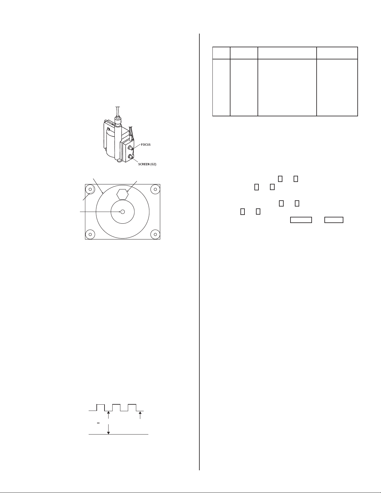
2-4. SCREEN (G2)
1. Input signal from the pattern generator.
White balance should be adjusted after Sub Contrast because
RDRV is also used in Sub Contrast Adjustment. (See page 19).
2. Set the user controls to NORMAL.
3. Attach the G2-Jig to the C Board.
4. Adjust RCUT, GCUT, BCUT, and SBRT in service mode with an
oscilloscope so that voltages on the red, green, and blue cathodes
are 170 ± 2.0 V DC.
5. Observe the screen and adjust SCREEN (G2) VR to obtain the faintly
visible background of the dot signal.
6. Push the TEST + JUMP (+ Channel) to cut off the signal. The screen
should be bright or dark. Brightness of raster must be increased
when adjusting.
7. Adjust screen VR until the screen is slightly cut off, or scarcely lights
up. A signal cannot be seen when the brightness of the raster is
high.
8. Push the JUMP again to release the cut off.
170 + 2.0 Vdc
GND
170Vdc
pedestal
— 11 —
SECTION 3: SAFETY RELATED ADJUSTMENTS
KV-29FV16A
3-1. X R530, R531 CONFIRMATION
METHOD (HOLD-DOWN
CONFIRMATION) AND
READJUSTMENTS
Always perform the following adjustments when replacing the following
components marked with a
Part Replaced (Y)
A BOARD:
C531, C532, D302, D519, D520,
Y
mark on the schematic diagram:
Adjustment (
A BOARD:
R530, R531
X
)
D521, IC355, IC501, Q301, R356,
R359, R361, R529, R530, R531,
R532, R533, R550, T503
GA BOARD
IC6003, R6088
PREPARATION BEFORE CONFIRMATION
1. Turn the POWER switch ON.
2. Input a white signal and set the PICTURE and BRIGHT controls to
maximum.
3. Confi rm that the voltage of more than 23.0 VDC appears between
TP85 and ground on the A Board.
4. Using a Variac, apply AC input voltage: 120 ± 2.0 VAC.
5. Input a white signal and verify that the I ABL is within the sepcifi ed
range: 1730.0 ± 100µA, +B = 135.0 ± 1.0 V DC.
At AC input: 120.0 ± 2.0 V AC.
T503
FBT
ammeter
3.0 mA DC
range
ABL
+
-
A
I ABL
digital
+
-
multimeter
R531
R530
DC Power Supply
TP85
+
-
T503
FBT
ammeter
3mA DC range
A
+
-
Lower than 24.78 ± (-0.1) V DC.
At AC input 120.0 ± 2.0 V AC.
8. A BOARD - CONDUCTOR SIDE: Confi rm that a voltage appears
between TP85 and ground of more than 21.0 V DC.
3-2. B+ VOLTAGE CONFIRMATION AND
ADJUSTMENT
Always perform the following adjustments when replacing the following
components, which are marked with
the GA Board:
GA BOARD: IC6003, R6088
1. Using a Variac, apply AC input voltage: 130 ± 2.0 VAC
2. Input a monoscope signal.
3. Set the PICTURE control and the BRIGHT control to initial reset
value.
4. Confi rm the voltage of GA Board CN6007 between pin
is less than 135.0 ± 1.5 V DC.
5. If step 4 is not satisfi ed, replace the R6088 on GA Board and repeat
the above steps.
Y
on the schematic diagram on
1
to ground
6. Record the voltage between TP 85 and ground.
7. Using an external DC power supply, apply voltage between TP85 and
ground. Increase the voltage gradually and confi rm that the hold
down works (raster disappears) at lower than the voltage recorded
in Step 6.
— 12 —
SECTION 4: CIRCUIT ADJUSTMENTS
ELECTRICAL ADJUSTMENTS BY REMOTE COMMANDER
Use the Remote Commander (RM-Y171) to perform the circuit adjustments in this section.
Test Equipment Required: 1. Pattern generator 2. Frequency counter 3. Digital multimeter 4. Audio oscillator
KV-29FV16A
4-1. SETTING THE SERVICE ADJUSTMENT
MODE
1. Standby mode (Power off).
2. Press the following buttons on the remote commander within a
second of each other:
DISPLAY
Channel 5 Sound Volume
+
Power
SERVICE ADJUSTMENT MODE IN
Register Item
Device Item Data Item
SERVICE VP VPOS 30
1000 0
3. The CRT displays the item being adjusted.
4. Press 2 or 5 on the Remote Commander to select the device item.
5. Press
6. Press
7. To recover the latest values, press
8. Press
1
or 4 on the Remote Commander to select the item.
3
or 6 on the Remote Commander to change the data.
0
ENTER
MUTING
then
then
ENTER
to write into memory**.
.
Note: If the NVM is replaced, perform this test and reset. Then
download from microprocessor to NVM to prevent loss of
picture.
SERVICE ADJUSTMENT MODE MEMORY
Register Item
Device Item Data Item
SERVICE VP VPOS 30
1000 0
MUTING
Green
SERVICE WRITE
1000 0000
Factory original setting
10. Turn set off and on to exit.
4-2. MEMORY WRITE CONFIRMATION
METHOD
1. After adjustment, pull out the plug from the AC outlet, then replace the
plug in the AC outlet again.
2. Turn the power switch ON and set to Service Mode.
3. Call the adjusted items again to confi rm they were adjusted.
4-3. REMOTE ADJUSTMENT BUTTONS AND
INDICATORS
VTR/DVD
FREEZE
SLEEP
SAT/CABLE
FUNCTION
SAT/CABLE
SWAP PIP
AUDIO
CHVOL
ENTER
POWER
TV/VIDEO
TV/VIDEOANT
DISPLAYMTS/SAP
GUIDE
RM-Y171
TV
TV
POWER
(Service mode)
DISPLAY
(Service mode)
3
(Data up)
6
(Data down)
5
(Device item down)
ENTER
(Write into memory)
0
(Read out of memory)
(Write into memory)
MUTING
1
(Item up)
2
(Device item up)
4
(Item down)
8
(Initialize)
VOL (+)
(Service mode)
MUTING
VTR/DVD
SYSTEM
OFF
TV/VTR
+
CH
POSITION
Ð
PICTURE
MODE
1 2 3
4 5 6
7 809
JUMP
TV/SAT
RESET MENU
CODE SET
Red
9. Press
then
8
ENTER
ENTER
on the Remote Commander to initialize.
Note: Carry out this step when adjusting IDs 0 to 4 and when
replacing IC102.
— 13 —
TV
RM-Y171
** WARNING: Do NOT turn off the power or remove the AC cord
immediately after pressing
MUTING
then
ENTER
. Wait at
least 10 seconds
SERVICE DATA
V
V
KV-29FV16A
No. Initial Data Average Data
Name
DescriptionRegister
Range
Adj/FixData
NTSC
PAL-M
PAL-N
TV/AUX
S/VIDEO 1-3
VIDEO 4
NTSC
PAL-M
PAL-N
TV/AUX
S/VIDEO 1-3
VIDEO 4
P CXA2135S
1 HPOS Horizontal Position Adjust 0-31 Fix 7 7
2 HSIZ Horizontal Amp Adjust 0-31 Fix 10 10
3 VBOW VRT Line Bowing Adjust 0-15 Fix6666
4 VANG VRT Line Bow Slant Adjust 0-15 Fix5555
5 TRAP Horizontal Trapezoid Adjust 0-15 Fix6666
6 PAMP Horizontal Pin Distort Adjust 0-63 Fix 32 32
7 UCPN Upper Pin 0-63 Fix 36 36
8 LCPN Lower Pin 0-63 Fix 36 36
9 VSIZ Vertical Amplitude Test 0-63 Fix 0 0
10 VPOS Vertical Position Test 0-63 Fix 31 31
11 VLIN Vertical Linearity Adjust 0-15 Fix 7 7
12 VSCO S-Correction 0-15 Fix 7 7
13 VZOM 16:9 CRT Z Mode On/Off 0,1 Fix0000
14 EHT VRT High Volt Correction 0-15 Fix4444
15 ASP Aspect Ratio Control 0-63 Fix47474747
16 SCRL 16:9 CRT Z Mode Tran Scroll 0-63 Fix31313131
17 HBSW HBLK SW 0,1 Fix1111
18 LBLK Left Screen H Blk Control 0-15 Fix15151515
19 RBLK Right Screen H Blk Control 0-15 Fix0000
20 HDW H Drive Pulse Width 0,1 Fix0011
21 EWDC EW/DC Adjust 0,1 Fix0000
22 LVLN Screen Bottom VRT Lin Adjust 0-15 Fix0000
23 UVLN Screen Top VRT Lin Adjust 0-15 Fix0000
24 RDRV R Output Drive Control 0-63 Adj 31 31 31 31
25 GDRV G Output Drive Control 0-63 Adj 31 31 31 31
26 BDRV B Output Drive Control 0-63 Adj 31 31 31 31
27 RCUT R Output Cutoff Control 0-15 Adj 7777
28 GCUT G Output Cutoff Control 0-15 Adj 7777
29 BCUT B Output Cutoff Control 0-15 Adj 7777
30 RDR4 Video 4 R Output Drive Control 0-63 Adj 31 31 31 31
31 GDR4 Video 4 G Output Drive Control 0-63 Adj 31 31 31 31
32 BDR4 Video 4 B Output Drive Control 0-63 Adj 31 31 31 31
33 RCU4 Video 4 R Output Cutoff Control 0-15 Adj 7777
34 GCU4 Video 4 G Output Cutoff Control 0-15 Adj 7777
35 BCU4 Video 4 B Output Cutoff Control 0-15 Adj 7777
36 SHUE Sub Hue 0-31 Adj 7 7 15 15
37 SCOL Sub Color 0-31 Adj 15 15
38 SBRT Sub Brightness 0-63 Fix15151515
39 RON R Output On/Off 0,1 Fix1111
40 GON G Output On/Off 0,1 Fix1111
41 BON B Output On/Off 0,1 Fix1111
42 AXPL Axis Pal 0,1 Fix0000
43 CBPF Chroma BPF On/Off 0,1 Fix 1 1
44 COFF Color On/Off 0,1 Fix0000
45 KOFF Set Color Killer 0,1 Fix0000
46 SSHP Sub Sharpness 0-15 Fix 7 7
47 SHPF Sharpness Circuit F0 0,1 Fix 1 1
48 PREL Pre/Over-Shoot Switching 0,1 Fix1111
49 Y-DC DC Trans Radio Switching 0,1 Fix1111
50 ABLM ABL Mode Switching 0,1 Fix1111
51 YDEL Y Delay Time Control 0-15 Fix 7 7
52 NCOL No Color ID 0,1 Fix1111
53 FSC FSC Out On/Off 0,1 Fix1111
54 K-ID Killer ID 0,1 Fix1111
55 HOSC H VCO Oscillation Frequency 0-15 Fix7777
56 VSS V Sync Slice Level 0,1 Fix0011
57 HSS H Sync Slice Level 0,1 Fix0011
58 HMSK H Mask 0,1 Fix1111
59
TMS Select Signal VTIM Pin 0-3 Fix0000
— 14 —
f
T
S
V
e
e
V
y
c
g
g
A
g
g
A
K
K
g
K
g
V
VTRR
V
V
V
t
g
SERVICE DATA (CONT.)
KV-29FV16A
No. Register
Name
VP CXA2135S
60 AFC AFC Loop Gain 0-3 Fix 0 0
61 FIFR Field Frequency 0-3 Fix3311
62 REFP REFP 0,1 Fix0000
63 VBSW VBW 0-3 Fix0000
64 BMOF Blk Off 0,1 Fix0000
65 AGN2 Aging 2 0,1 Fix0000
66 YSHU Hue for YUV Models 0-63 Fix 31 31 31 31
Description Data
Range
continued
Adj/Fix Initial Data Average Data
NTSC
PAL-M
PAL-N
TV/AUX
S/VIDEO 1-3
VIDEO 4
NTSC
PAL-M
PAL-N
S/VIDEO 1-3
VIDEO 4
TV/AUX
AP BH3868
67 BBLP BBE Low Pass 0-15 Fix0055
68 BBHP BBE High Pass 0-15 Fix0033
69 SVOL Sub Volume 0-15 Fix0077
70 SBAL Sub Balance 0-15 Fix7777
71 SBAS Sub Bass 0-15 Fix7755
72 STRE Sub Treble 0-15 Fix7755
AP TDA7467
73 SPCA SRS/Space Attenuation 0-63 Fix0000
74 CENA SRS/Center Attenuation 0-63 Fix0000
75 INPA Input Attenuation 0-127 Fix3333
3D UPD64081
76 HHDS HH Of
77 COU
78 YAP
79 NSDS Adaptiv
80 MSS Adaptiv
81 DYC Hi Impedence
82 EXAD Ext Ad Selected
83 PECS Standard
84 EXCS Use CSI Just in Case
85 CPP
86 HDP H Phase +/- 0µ sec
87 CDL Y/C Dela
88 DYCO Y Movin
89 DYG
90 DCCO C Movin
91 DCG
92 YNR
93 YNRI Effect Small
94 YNRL Noise Limit
95 CNR
96 CNRI Effect Small
97 CNRL CNR Limit
98 ID1O ID 1 Throu
99 ID1W 4:03
100 ID1N Normal
101 CL
102 ST1S Monitor Out
103 ST0S Monitor Out
104 WSC Corin
105
106
107 LDSR Frame
108 PWRE PWRE
109 PDRE PDRE
110 PBRE PBRE
111
112
113 TEST Tes
114 YPFT Y Peakin
Gain 1/BPF On
Comp/Y Eaking On
TB = 1.25 VPP
+/- 0µ se
Y Moving Gain
C Moving Gain
Effect Small
Effect Small
Low Fix
TRH H Non Standard DET
H Non Standard DET
APGV Apacon Gain
API
Apacon
Corin
Corin
h
0-3
0-3
0-3
0-3
0-3
0-3
0,1
0-3
0-3
0-3
0-7
0-7
0-15
0-15
0-15
0-15
0,1
0,1
0-3
0,1
0,1
0-3
0,1
0,1
0,1
0,1
0-3
0-3
0-3
0-3
0-3
0-3
0,1
0-7
0-15
0-7
0-31
0,1
0-3
Fix1111
Fix3333
Fix3333
Fix0000
Fix0000
Fix2222
Fix1111
Fix0000
Fix1111
Fix0000
Fix3333
Fix4444
Fix2222
Fix 10 10 10 10
Fix2222
Fix9999
Fix1111
Fix0000
Fix1111
Fix1111
Fix0000
Fix1111
Fix0000
Fix0000
Fix0000
Fix1111
Fix0000
Fix1111
Fix1111
Fix1111
Fix1111
Fix2222
Fix0000
Fix4444
Fix8888
Fix3333
Fix 10 10 10 10
Fix0000
Fix3333
— 15 —
SERVICE DATA (CONT.)
KV-29FV16A
No. Register
Name
3D UPD64081
Description Data
Range
continued
Adj/Fix Initial Data Average Data
NTSC
PAL-M
PAL-N
TV/AUX
S/VIDEO 1-3
VIDEO 4
NTSC
PAL-M
PAL-N
TV/AUX
S/VIDEO 1-3
VIDEO 4
115 YPFG Y Peaking Gain 0-15 Fix 10 10 10 10
116 V1PS Line Comb Dot H 0-3 Fix2222
117 VEGS Line Comb Dot V 0-3 Fix2222
118 CC3N C Width 0,1 Fix0000
119 C0HS C Delay On 0,1 Fix0000
120 CLPH Y-Ad Clamp Test 0,1 Fix0000
121 SEL2 DC Sensitivity Small 0,1 Fix0000
122 SEL1 DY Sensitivity Small 0,1 Fix0000
123 YHCO Coring Small 0-3 Fix2211
124 YPCO Coring On 0,1 Fix0000
125 ED20 Standard 0,1 Fix1111
126 OVST Standard 0,1 Fix0000
127 CSHD Standard 0,1 Fix0000
128 KCTT Standard 0-3 Fix0000
129 SHT1 Standard 0,1 Fix0000
130 SHT0 Standard 0,1 Fix0000
131 VCT Standard 0,1 Fix0000
132 OTT Standard 0,1 Fix0000
133 CGAT Standard 0,1 Fix0000
134 CGGT Standard 0,1 Fix0000
135 CGFT Standard 0,1 Fix0000
136 CGT Standard 0,1 Fix0000
137 HPLL Standard 0,1 Fix1111
138 BPLL Burst PLL Fast 0,1 Fix0000
139 FSCF Burst Gain Large 0,1 Fix0000
140 PLLF PLL Loop Gain Large 0,1 Fix1111
141 KILR Killer Lever 0-15 Fix3333
142 HSSL H Slice Level 0-15 Fix 12 12 12 12
143 VSSL V Slice Level 0-15 Fix8888
144 BGPS Start Burst Gate 0-15 Fix4444
145 BGPW Width of Burst Gate 0-15 Fix 10 10 10 10
146 ADCL ADC Clock 0-3 Fix3333
147 ADPD Adc Power Down On 0,1 Fix1111
148 ADLT Standard 0,1 Fix0000
149 NRZO Check On 0,1 Fix0000
150 FSCO Level Check On 0,1 Fix0000
151 VTVH Normal 0-3 Fix0000
152 TST2 Standard 0,1 Fix0000
153 HMEM Use CSI Just in Case 0,1 Fix1111
154 HINV Polarity of Reset 0,1 Fix1111
155 HTMG Field Memory Address 0,1 Fix0000
156 HCP HH Carrier Phase 0-15 Fix7777
157 TST3 Test 0,1 Fix0000
158 HHMG HH Moving Gain 0,1 Fix1111
159 HHFG HH Off 0-3 Fix0000
160 HHTG Max HH 0-15 Fix5555
PI TA1226N
161 SHPR Picture Improvement Sharpness 0-127 Fix 59 59 59 59
162 BLAD Picture Improvement Black Area Det. 0-3 Fix0000
163 SRTS Picture Improvement SRT Start Pos 0-3 Fix3333
164 YNR Picture Improvement YNR 0,1 Fix1111
165 GIRE Picture Improvement Gamma Start 0-3 Fix3333
166 DAC1 Picture Improvement DAC1 0,1 Fix1111
167 DAC2 Picture Improvement DAC2 0,1 Fix0000
168 GCUR Picture Improvement Gamma Curve 0,1 Fix0000
169 BLKC Picture Improvement Black Compen. 0,1 Fix1111
170 TEST Picture Improvement Test 0-3 Fix3333
171 RS Picture Improvement RS 0-7 Fix0000
172 RTC Picture Improvement RTC 0-7 Fix4444
— 16 —
SERVICE DATA (CONT.)
t
y
W
y
W
y
p
y
W
y
W
y
y
y
TDy
t
y
t
TDy
t
YDy
y
y
f
0Dy
0
y
y
(
(
(
y
(
)
(
)
(
)
(
)
(
(
(
0
(
2
(
(
(
(
(
(
(
T
C
A
J
R
KV-29FV16A
No. Register
Description Data
Name
DC CXA2060
173 DCSF Dynamic Convergence DC Shif
174 UYBW D
175 LYBW D
176 HAMP D
177 UCBW D
178 LCBW D
179 UMBH D
180 LMBH D
181 PWM D
182 HTL
183 UTLD D
184 LTL
185 HDT
186 TOFF D
187 DAC
188 DAC1 D
namic Convergence Upper YBO
namic Convergence Lower YBO
namic Convergence H. Am
namic Convergence H. CBO
namic Convergence L. CBO
namic Convergence U. MBH
namic Convergence L. MBH
namic Convergence PWM
namic Convergence H. Til
namic Convergence U. Til
namic Convergence L. Til
namic Convergence H. Dut
namic Convergence Tilt Of
namic Convergence DAC
namic Convergence DAC1
SP SDA9288
189 PYSD P in P (Seimens) YS Dela
190 PIPH P in P
191 PIPV P in P
192 PYDL P in P
193 PIFX P in P Inset Fixed
194 PPFX P in P Parent Fixed
195 PCLI P in P CLISW
196 PAMS P in P AMSEC
197 PHDL P in P
198 PMVD P in P
199 PIVD P in P
200 PCON P in P
201 FRMY P in P
202 CHRI P in P
203 CHRO P in P
204 MAT
205 MAT1 P in P
206 MAT
207 IPER P in P
208 IPEB P in P
209 PCPS P in P
210 PCPF P in P
211 PSEL P in P
212 PPLL P in P
213 PVNR P in P
Seimens) H-Position
Seimens) V-Position
Seimens) Y-Dela
Seimens) H-Pulse Delay (Ins
Seimens) V-Pulse Delay (Mn
Seimens) V-Pulse Delay (Ins
Seimens) Contrast Lvl (Ins
Seimens) Frame Y
Seimens) Chroma Input Pol.
Seimens) Chroma Output Pol.
P in P (Seimens) MAT0
Seimens) MAT1
P in P (Seimens) MAT2
Seimens) Pedestal R-Y
Seimens) Pedestal B-Y
Seimens) CLP & HSIDEL
Seimens) CLP Cycles
Seimens) SELDOWN
Seimens) PLL Filter
Seimens) VSP Pulse Noise R.
Range
0-63
0-63
0-63
0-63
0-63
0-63
0-63
0-63
0-63
0-63
0-63
0-63
0-3
0,1
0-255
0-255
0-15
0-127
0-63
0-7
0-3
0-3
0,1
0,1
0-15
0-31
0-31
0-15
0-15
0,1
0,1
0,1
0,1
0,1
0-15
0-15
0,1
0,1
0,1
0-3
0,1
Adj/Fix Initial Data Average Data
NTSC
PAL-M
PAL-N
TV/AUX
S/VIDEO 1-3
VIDEO 4
NTSC
PAL-M
PAL-N
TV/AUX
S/VIDEO 1-3
VIDEO 4
Fix32323232
Fix31313131
Fix31313131
Fix23232323
Fix14141414
Fix14141414
Fix 15 15 15 15
Fix 15 15 15 15
Fix 63 63 63 63
Fix63636363
Fix63636363
Fix63636363
Fix3333
Fix1111
Fix 255 255 255 255
Fix 255 255 255 255
Fix2222
Fix 78 78 78 78
Fix 18 18 18 18
Fix0000
Fix0000
Fix0000
Fix1111
Fix0000
Fix15151515
Fix11111111
Fix18181818
Fix3333
Fix 10 10 10 10
Fix0000
Fix0000
Fix1111
Fix0000
Fix1111
Fix0000
Fix0000
Fix0000
Fix0000
Fix1111
Fix0000
Fix0000
IC CXA2019
214 IDPX
215 ICOL Color
216 ISHP Sharpness
217 ISCO Sub Chroma Decoder Sub Cont
218 ISCL Sub Chroma Decoder Sub Color
219 ISHU Sub Chroma Decoder Sub Hue
220 ITO
Sub Chroma Decoder Tot On
221 ITRP Sub Chroma Decoder Trap On
222 IAFC AF
223 ITR
Sub Chroma Decoder CTRAP AD
224 ICD2 Sub Chroma Decoder CD Mode2
225 ISF0 SHP-F0
226 IYD
Sub Chroma Decoder Y Drive
227 IVPE Sub Chroma Decoder V Ped
228 IUPE Sub Chroma Decoder U Ped
229 IRVP Sub Chroma Decoder RV Ped
230 IRUP Sub Chroma Decoder RU Ped
0,1
0-63
0-15
0-15
0-15
0-15
0,1
0,1
0-3
0-15
0,1
0,1
0-31
0-15
0-15
0-15
0-15
— 17 —
Fix0000
Fix38383838
Fix 10 10 10 10
Fix7777
Fix 8 8
Fix7777
Fix0000
Fix1111
Fix 1 1
Fix 7 7
Fix 1 1
Fix1111
Fix 24 24 24 24
Fix0000
Fix0000
Fix9999
Fix7777
KV-29FV16A
y
n
t
y
r
t
y
y
g
y
K
Y
y
y
y
y
y
y
y
SERVICE DATA (CONT.)
Description Data
Name
IC CXA2019
231 IDCT Sub Chroma Decoder DC Tran
232 IRYD Sub Chroma Decoder RY Drive
233 IPRE Sub Chroma Decoder Pre Over
234 IRUD Sub Chroma Decoder RU Drive
235 IRVD Sub Chroma Decoder RV Drive
236 IDLV Sub Chroma Decoder Dela
237 ISCR Sub Chroma Decoder SCP BGR
238 ISCF Sub Chroma Decoder SCP BGF
continued
Range
0-7
0-31
0-3
0-31
0-31
0-3
0-3
0-3
Adj/Fix Initial Data Average DataNo. Register
NTSC
PAL-M
PAL-N
Fix4466
Fix 19 19 19 19
Fix1111
Fix8888
Fix8888
Fix 0 0
Fix1111
Fix1111
TV/AUX
S/VIDEO 1-3
VIDEO 4
NTSC
PAL-M
PAL-N
TV/AUX
S/VIDEO 1-3
VIDEO 4
DA CXA1315
239 IDPX D/A Converter N-S Correctio
240 ICOL Color
241 ISHP Sharpness
242 ISCO Sub Chroma Decoder Sub Cont
243 ISCL Sub Chroma Decoder Sub Color
0-63
0-255
0-255
0-31
0-31
Fix 32 32 32 32
Fix 120 120
Fix 120 120 120 120
Fix 15 15
Fix 1 1 15 15
D1 CXD2085
244 XJGL XJGLK 0,1 Fix0000
245 LNJ1 LNJ1 0,1 Fix0000
CC CXP85856A
246 CRIL CCD CRI Pulse Compare Data Low
247 CFLD CCD Caption Fixed-Field Count
248 CCDI CCD No CCD Interrup
249 CRIP CCD CRI & Parit
250 CRIT CCD CRI Time Constan
251 CSB1 CCD S
252 CSB2 CCD S
253 CREP CCD CRI Si
254 CDSD CCD Data Start Dela
255 CCDS CCD Caption Data Threshold
256 CHMK CCD P8-HMAS
257 CHS
CCD P8-HSYC
nc Slice Bias 1
nc Slice Bias 2
Erro
nal End Position
0-15
0-15
0-7
0-7
0-3
0-3
0-7
0-256
0-31
0-31
0-63
0-255
Fix2222
Fix5555
Fix3333
Fix4444
Fix0000
Fix3333
Fix4444
Fix 142 142 142 142
Fix8888
Fix9999
Fix 42 42 42 42
Fix 136 136 136 136
OP CXP85856A
258 DISP OSD Position 0-63 Fix1111
No. Register
Name
Description Data
Range
Adj/Fix Initial Data Average Data ID
NTSC
PAL-M
PAL-N
TV/AUX
S/VIDEO 1-3
VIDEO 4
NTSC
PAL-M
PAL-N
TV/AUX
S/VIDEO 1-3
VIDEO 4
ID MAP
259 IDCT NVM ID 0
260 IRYD NVM ID 1
261 IPRE NVM ID 2
262 IRUD NVM ID 3
263 IRVD NVM ID 4
264 IDLV NVM ID 5
265 ISCR NVM ID 6
266 ISCF NVM ID 7
0-7
0-31
0-3
0-31
0-31
0-3
0-3
0-3
Fix by model 89 89 63 63 31
Fix b
model 55 55 55 55 63
Fix b
model 175 175 175 175 175
Fix b
model 96 96 64 64 192
Fix b
model 203 203 251 251 251
Fix b
model 181 181 181 181 181
Fix b
model 66666
Fix b
model 9900112
SERVICE IDO WRITE
Note: Items 1-266 show
adjustment order
— 18 —
KV-29FV16A
4-4. A BOARD ADJUSTMENTS
SUB BRIGHT ADJUSTMENT
1. Set to Service Adjustment Mode.
2. Input a grey scale pattern signal.
3. Set the PICTURE to minimum, and BRIGHT to normal.
white
1
and 4 .
3
and 6 so that the stripe second
MUTING
second from the right
black
then
ENTER
.
4. Select SBRT with
5. Adjust SUB BRIGHT level with
from the right is faintly visible.
6. Write into memory by pressing
SUB CONTRAST ADJUSTMENT (RDRV)
1. Input a 75% color-bar signal.
2. Set to: VIDEO mode = Standard, COLOR = Minimum, PICTURE =
100%, GON = 0 (OFF), BON = 0 (OFF)
3. Set to Service Adjustment Mode and connect an oscilloscope to pin
of CN351 on the A Board.
1
4
3
and
1
.
and
6
for: 1.85 ± 0.05 Vp-p.
MUTING
White
1.85 ± 0.05Vp-p
then
ENTER
.
4. Set RDRV with
5. Adjust with
6. Write into memory by pressing
V. SIZE ADJUSTMENT (VSIZ)
1. Input a monoscope signal.
2. Set to Service Adjustment Mode.
4
3
and
1
3. Select VSIZ with
4. Adjust with
5. Write into memory by pressing
.
and
6
for the best vertical size.
MUTING
then
ENTER
V. SIZE
V. POSITION ADJUSTMENT (VPOS)
1. Input a monoscope signal.
2. Set to Service Adjustment Mode.
4
3
and
1
6
.
and
for the best vertical center.
MUTING
then
ENTER
3. Select VPOS with
4. Adjust with
5. Write into memory by pressing
V. POSITION
H. SIZE ADJUSTMENT (HSIZ)
1. Input a monoscope signal.
2. Set to Service Adjustment Mode.
4
3. Select HSIZ with
4. Adjust with 3 and
5. Write into memory by pressing
H. SIZE
1
.
and
6
for the best horizontal size.
MUTING
then
ENTER
.
.
.
Black
SUB HUE, SUB COLOR ADJUSTMENT
(SHUE, SCOL, 4SHU, 4COL)
Note: SCOL and SHUE are for all other inputs (NTSC/PAL M/PAL N)
4SHU and 4COL are for Video 4 input (NTSC/PAL M/PAL N)
1. Input a 75% color-bar signal.
2. Set to Service Adjustment Mode and set: VIDEO mode = Standard,
PICTURE = 100%, COLOR = 50%, HUE = 50%.
3. Connect an oscilloscope to Pin
4. Select SHUE and SCOL with
3
6
5. Adjust with
6. Write SHUE data one step down from even condition to NVM.
SCOL is adjusted by SHUE compensation.
7. Write into memory by pressing
8. Repeat Steps 1-7 for 4SHU and 4COL.
and
for the V1 = V4 (SCOL) and V2 = V3 (SHUE).
V1
3
of CN351 on the A Board.
4
1
V2 V3
.
and
MUTING
V4
then
ENTER
.
H. POSITION ADJUSTMENT (HPOS)
HPOS Range is from 0~15.
1. Input a monoscope signal.
2. Set to Service Adjustment Mode.
4
3
and
1
6
.
and
for the best horizontal center.
MUTING
then
ENTER
3. Select HPOS with
4. Adjust with
5. Write into memory by pressing
H. POSITION
.
— 19 —
KV-29FV16A
V LINEARITY (VLIN), V CORRECTION (VSCO),
PIN AMP (PAMP) AND TRAPEZIUM (TRAP)
ADJUSTMENTS
1. Input a cross-hatch signal.
2. Set to Service Adjustment Mode.
4
3. Select VLIN, VSCO, PAMP, and TRAP with
3
6
4. Adjust with
5. Write into memory by pressing
and
for the best picture.
MUTING
V LINEARITY(VLIN)
VS CORRECTION (VSCO)
PIN AMP (PAMP)
TRAPEZIUM (TRAP)
1
then
and
ENTER
.
.
OSD POSITION ADJUSTMENT (DISP)
1. Input a color-bar signal.
2. Set to Service Adjustment Mode.
4
3
and
1
3. Select DISP with
4. Adjust with
5. Write into memory by pressing
.
and
6
for the bar center.
MUTING
SERVICE
1000 0000
then
AFC 0
ENTER
.
ROTATION COIL ADJUSTMENT
1. Input a monoscope signal.
2. Push
3. Select the “Set-up” mode.
4. Select “Tilt Correction”. Confi rm that number (0) color changes to red.
5. Push
+5 and the picture rotates clockwise.
6. Push
to -5 and the picture rotates counter-clockwise.
7. Push
on the Remote (RM-Y171).
MENU
(+) on the Remote. Confi rm that the number increases up to
(-) on the Remote. Confi rm that the number decreases down
(+) on the Remote. Return the value to 0.
V ANGLE (VANG), V BOW (VBOW), UPPER
UPPER PIN (UCPN) AND LOW PIN (LCPN)
ADJUSTMENTS
1. Input a cross-hatch signal.
2. Set to Service Adjustment Mode.
4
then
1
and
ENTER
.
.
3. Select VANG, VBOW, UCPN, and LCPN with
3
6
4. Adjust with
5. Write into memory by pressing
and
for the best picture.
MUTING
V ANGLE (VANG)
V BOW (VBOW)
UPPER PIN (UCPN)
LOW PIN (LCPN)
SET-UP
+5
Channel Set-up
Favorite Channel
Video Label
Language: English
Tilt Correction
Menu
-5
— 20 —
5-1. CIRCUIT BOARDS LOCATION
HX Board
SECTION 5: DIAGRAMS
The components identifi ed by shading and ! symbol are critical for safety. Replace
only with part number specifi ed.
The symbol indicates a fast operating fuse and is displayed on the component
side of the board. Replace only with fuse of the same rating as marked.
C Board
Les composants identifi es par un trame et une marque
HB Board
securite. Ne les remplacer que par une piece portant le numero specifi e.
KV-29FV16A
!
sont critiques pour la
HZ Board
WA Board
HA Board
AK Board
GA Board
A Board
UY Board
5-2. PRINTED WIRING BOARDS AND
SCHEMATIC DIAGRAMS INFORMATION
All capacitors are in µF unless otherwise noted. pF : µµF 50WV or less
are not indicated except for electrolytics and tantalums.
All electrolytics are in 50V unless otherwise specifi ed.
All resistors are in ohms. KΩ=1000Ω, MΩ=1000kΩ
Indication of resistance, which does not have one for rating
electrical power, is as follows: Pitch : 5mm
Rating electrical power :
1
/
W in resistance, 1/
4
W and 1/
10
8
: nonfl ammable resistor.
: fusible resistor.
: internal component.
: panel designation and adjustment for repair.
All variable and adjustable resistors have characteristic curve B, unless
otherwise noted.
Readings are taken with a color-bar signal input.
Readings are taken with a 10MΩ digital multimeter.
Voltages are DC with respect to ground unless otherwise noted.
Voltage variations may be noted due to normal production tolerances.
All voltages are in V.
S : Measurement impossibillity.
: B+line.
: B-line. (Actual measured value may be different).
: signal path. (RF)
Circled numbers are waveform references.
1
/
W
4
W in chip resistance.
Le symbole
fusible de meme yaleur, comme maque.
indique une fusible a action rapide. Doit etre remplace par une
The components identifi ed by X in this basic schematic diagram have
been carefully factory-selected for each set in order to satisfy regulations
regarding X-ray radiation. Should replacement be necessary, replace
only with the value originally used (Refer to Safety Related Adjustments
on page 12).
When replacing components identifi ed by
Y
, make the necessary
adjustments as indicated. If the results do not meet the specifi ed value,
change the component identifi ed by
X
and repeat the adjustment until
the specifi ed value is achieved.
When replacing the parts listed in the table below, it is important to
perform the related adjustments.
Part Replaced (Y) Adjustment (X)
A BOARD:
C531, C532, D302, D519, D520,
A BOARD:
R530, R531
D521, IC355, IC501, Q301, R356,
R359, R361, R529, R530, R531,
R532, R533, R550, T503
GA BOARD
IC6003, R6088
REFERENCE INFORMATION
RESISTOR
: RN METAL FILM
: RC SOLID
: FPRD NONFLAMMABLE CARBON
: FUSE NONFLAMMABLE FUSIBLE
: RW NONFLAMMABLE WIREWOUND
: RS NONFLAMMABLE METAL OXIDE
: RB NONFLAMMABLE CEMENT
: ADJUSTMENT RESISTOR
COIL
: LF-8L MICRO INDUCTOR
CAPACITOR
: TA TANTALUM
: PS STYROL
: PP POLYPROPYLENE
: PT MYLAR
: MPS METALIZED POLYESTER
: MPP METALIZED POLYPROPYLENE
: ALB BIPOLAR
: ALT HIGH TEMPERATURE
: ALR HIGH RIPPLE
— 21 —
 Loading...