


HISTORY INFORMATION FOR THE FOLLOWING MANUAL:
SERVICE MANUAL
MODEL NAME REMOTE COMMANDER DESTINATION CHASSIS NO.
KV-27FV300
KV-27FV300
KV-29FV300
KV-29FV300
KV-32FV300
KV-32FV300
KV-36FV300
KV-36FV300
KV-36FV300
RM-Y181 US SCC-S65AA
RM-Y181 CND SCC-S64AA
RM-Y181 LATIN NORTH SCC-S62BA
RM-Y181 LATIN SOUTH SCC-S62CA
RM-Y182 US SCC-S65BA
RM-Y182 CND SCC-S64BA
RM-Y182 US SCC-S65CA
RM-Y182 CND SCC-S64CA
RM-Y182 HAWAII SCC-S67AA
BA-5D
CHASSIS
ORIGINAL MANUAL ISSUE DATE: 3/2002
ALL REVISIONS AND UPDATES TO THE ORIGINAL MANUAL ARE APPENDED TO THE END OF THE PDF FILE.
REVISION DATE REVISION TYPE SUBJECT
3/2002 No revisions or updates are applicable at this time.
5/2002 Correction - 1 Critical parts incorrectly indentied in Exploded View, Electrical Parts
List, A Board Schematic.
10/2002 Correction - 2 Exploded View PN correction for Door
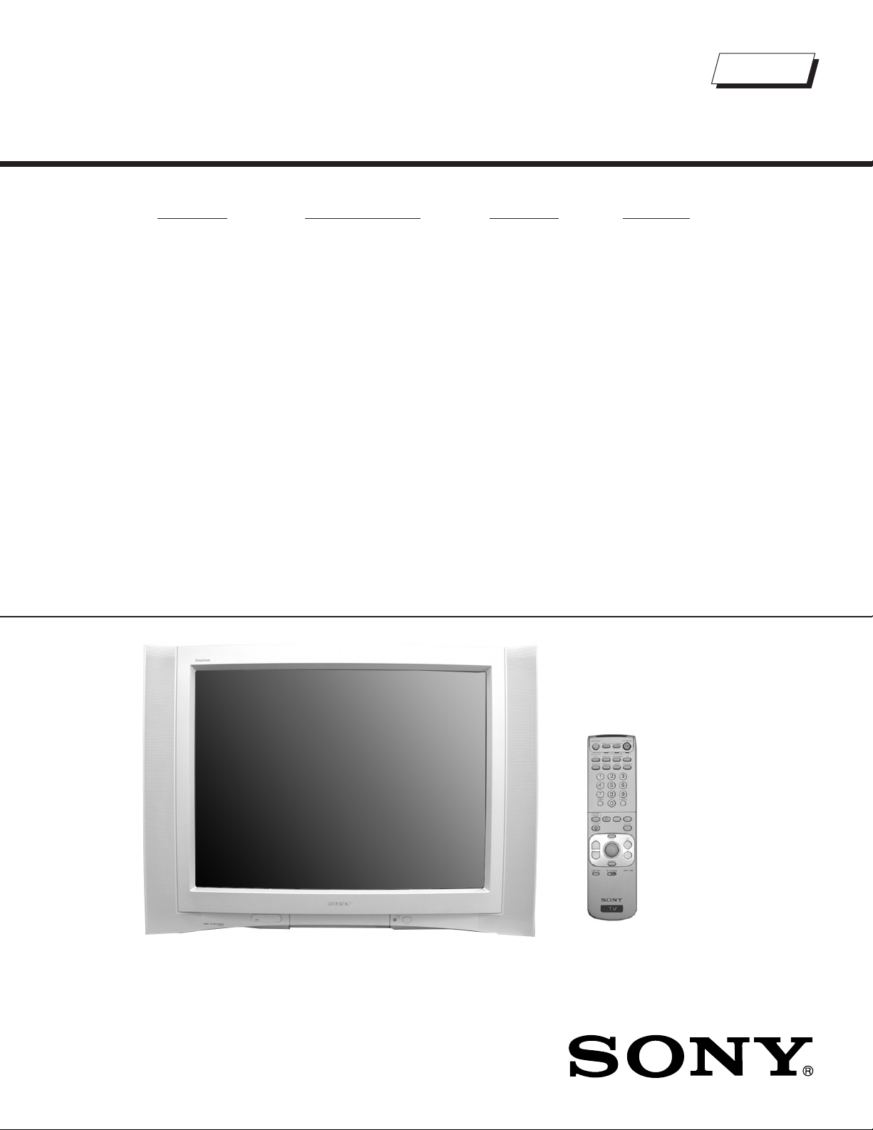
TRINITRON® COLOR TELEVISION
9-965-924-03
Self Diagnosis
Supported model
SERVICE MANUAL
MODEL NAME REMOTE COMMANDER DESTINATION CHASSIS NO.
KV-27FV300
KV-27FV300
KV-29FV300
KV-29FV300
KV-32FV300
KV-32FV300
KV-36FV300
KV-36FV300
KV-36FV300
RM-Y181 US SCC-S65AA
RM-Y181 CND SCC-S64AA
RM-Y181 LATIN NORTH SCC-S62BA
RM-Y181 LATIN SOUTH SCC-S62CA
RM-Y182 US SCC-S65BA
RM-Y182 CND SCC-S64BA
RM-Y182 US SCC-S65CA
RM-Y182 CND SCC-S64CA
RM-Y182 HAWAII SCC-S67AA
BA-5D
CHASSIS
9-965-924-03
KV-36FV300 RM-Y182
TRINITRON® COLOR TELEVISION

KV-27FV300/29FV300/32FV300/36FV300
TABLE OF CONTENTS
SECTION TITLE PAGE
Specifi cations........................................................................................................................................ 4
Warnings and Cautions.........................................................................................................................5
Safety Check-Out ................................................................................................................................. 6
Self-Diagnostic Function.......................................................................................................................7
1. Disassembly
1-1. Rear Cover Removal ................................................................................................................... 10
1-2. Chassis Assembly Removal ........................................................................................................ 10
1-3. Service Position...........................................................................................................................10
1-4. Picture Tube Removal ................................................................................................................. 11
Anode Cap Removal Procedure.................................................................................................. 11
2. Set-up Adjustments
2-1. Beam Landing ............................................................................................................................. 12
2-2. Convergence ............................................................................................................................... 13
2-3. Focus...........................................................................................................................................15
2-4. Screen (G2) ................................................................................................................................. 15
2-5. White Balance Adjustments......................................................................................................... 15
3. Safety Related Adjustments
3-1.
3-2. B+ Voltage Confi rmation and Adjustment.................................................................................... 16
4. Circuit Adjustments
4-1. Setting Service Adjustment Mode................................................................................................17
4-2. Memory Write Confi rmation Method ............................................................................................ 17
4-3. Remote Adjustment Buttons and Indicators ................................................................................ 17
4-4. Service Data Lists........................................................................................................................ 18
4-5. ID Map Table ............................................................................................................................... 26
4-6. Board Adjustments ...................................................................................................................... 26
5. Diagrams
5-1. Circuit Board Location ................................................................................................................. 29
5-2. Printed Wiring Board and Schematic Diagrams Information ....................................................... 29
5-3. Block Diagram and Schematics................................................................................................... 30
A Board Schematic Diagram .......................................................................................................31
BC Board Schematic Diagram .................................................................................................... 39
HU Board Schematic Diagram..................................................................................................... 42
P Board Schematic Diagram .......................................................................................................44
HR Board Schematic Diagram..................................................................................................... 46
T Board Schematic Diagram........................................................................................................ 47
C Board Schematic Diagram ....................................................................................................... 48
V Board Schematic Diagram .......................................................................................................50
GK Board Schematic Diagram..................................................................................................... 52
5-4. Semiconductors...........................................................................................................................54
X
R530, R531 Confi rmation Method (Hold-Down Confi rmation) and Readjustments ............... 16
6. Exploded Views
6-1. Chassis (KV-27FV300/29FV300 ONLY) ...................................................................................... 55
6-2. Picture Tube (KV-27FV300/29FV300 ONLY) ..............................................................................56
6-3. Chassis (KV-32FV300 ONLY) ..................................................................................................... 57
6-4. Picture Tube (KV-32FV300 ONLY) .............................................................................................. 58
6-5. Chassis (KV-36FV300 ONLY) ..................................................................................................... 59
6-6. Picture Tube (KV-36FV300 ONLY) .............................................................................................. 60
7. Electrical Parts List ..................................................................................................................................... 61
— 3 —
Power Requirements
Number of Inputs/Outputs
Speaker Output (W)
Power Consumption (W)
Dimensions (W xHxD)
Mass
Television system
American TV standard, NTSC
Channel coverage
VHF: 2-13/ UHF: 14-69/ CATV: 1-125
Picture tube
FD Trinitron® tube
KV-27FV300/29FV300/32FV300/36FV300
SPECIFICATIONS
KV-27FV300
KV-29FV300
Video
S Video
Y, PB,P
Audio
Audio Out
1)
2)
3)
R
4)
5)
Monitor Out
In Use (Max) 230 W 230 W
In Standby 1W 1W
mm 898 x 682 x 584 mm 1020 x 760 x 640 mm
784 x 601.5 x 520 mm
30
in 35
kg 78 kg 102 kg
lbs
220 W
1W
7/8
x23
11/16
x20
48 kg
105 lbs. 13 oz.
1/2
in
KV-32FV300 KV-36FV300
120V, 60Hz
3
2
1
3
1
1
7.5Wx2,
15 Wsubwoofer
3/8
7/8
x26
x23in 40
1/4
x30x25
171 lbs. 15 oz. 224 lbs. 14 oz.
1)
1 Vp-p 75 ohms unbalanced, sync negative
2)
Y: 1 Vp-p 75 ohms unbalanced, sync negative
C: 0.286 Vp-p (Burst signal), 75 ohms
3)
Y: 1.0 Vp-p, 75 ohms, sync negative;
PB: 0.7 Vp-p, 75 ohms
PR: Vp-p, 75 ohms
4)
500 mVrms (100% modulation), Impedance: 47 kilohms
)
More than 408 mVrms at the maximum volume setting (variable)
5
More than 408 mVrms (fi x)
1/4
in
Visible screen size
27 inch picture measured diagonally (KV-27FV300/29FV300)
32 inch picture measured diagonally (KV-32FV300)
36 inch picture measured diagonally (KV-36FV300)
Actual screen size
29 inch measured diagonally (KV-27FV300/29FV300)
34 inch measured diagonally (KV-32FV300)
38 inch measured diagonally (KV-36FV300)
Antenna
75-ohm external antenna terminal for VHF/UHF
Supplied Accessories
Size AA (R6) batteries (2)
Remote Control RM-Y181 (1) (KV-27FV300/29FV300)
Remote Control RM-Y182 (1) (KV-32FV300/36FV300)
Wireless Headphones (1) (KV-32FV300/36FV300)
Optional Accessories
TV Stand: SU-27HV2 for (KV-27KV300/29FV300)
SU-32HV3 for (KV-32KV300)
SU-36HV3 for (KV-36KV300)
Design and specifi cations are subject to change without notice.
TruSurround is a trademark of
SRS Labs, Inc. SRS and the SRS
symbol are registered trademarks
™
TruSurround
incorporated under license from SRS Labs, Inc. and are protected
under United States Patent Nos. 4,748,669 and 4,841,572 with
numerous additional issued and pending foreign patents. Purchase of this product does not convey the right to sell recordings
made with the TruSurround technology.
by SRS
of SRS Labs, Inc. in the United
States and in select foreign coun-
®
tries. SRS and TruSurround are
(•) SRS (SOUND RETRIEVAL SYSTEM)
The (•) SRS (SOUND RETRIEVAL SYSTEM) is manufactured by Sony
Corporation under license from SRS Labs, Inc. It is covered by U.S. Patent No.
4,748,669. Other U.S. and foreign patents pending.
The word ‘SRS’ and the SRS symbol (•) are registered trademarks of SRS
Labs, Inc. BBE and BBE symbol are trademarks of BBE Sound, Inc. and are
licensed by BBE Sound, Inc. under U.S. Patent No. 4,638,258 and 4,482,866.
— 4 —

KV-27FV300/29FV300/32FV300/36FV300
WARNINGS AND CAUTIONS
CAUTION
Short circuit the anode of the picture tube and the anode cap to the metal chassis, CRT shield, or carbon painted on the CRT,
after removing the anode.
WARNING!!
An isolation transformer should be used during any service to avoid possible shock hazard, because of live chassis. The chassis of
this receiver is directly connected to the ac power line.
! SAFETY-RELATED COMPONENT WARNING!!
Components identifi ed by shading and ! mark on the schematic diagrams, exploded views, and in the parts list are critical for
safe operation. Replace these components with Sony parts whose part numbers appear as shown in this manual or in supplements
published by Sony. Circuit adjustments that are critical for safe operation are identifi ed in this manual. Follow these procedures
whenever critical components are replaced or improper operation is suspected.
ATTENTION!!
Apres avoir deconnecte le cap de l’anode, court-circuiter l’anode du tube cathodique et celui de l’anode du cap au chassis metallique
de l’appareil, ou la couche de carbone peinte sur le tube cathodique ou au blindage du tube cathodique.
Afi n d’eviter tout risque d’electrocution provenant d’un chássis sous tension, un transformateur d’isolement doit etre utilisé lors de tout
dépannage. Le chássis de ce récepteur est directement raccordé à l’alimentation du secteur.
! ATTENTION AUX COMPOSANTS RELATIFS A LA SECURITE!!
Les composants identifi es par une trame et par une marque ! sur les schemas de principe, les vues explosees et les listes de
pieces sont d’une importance critique pour la securite du fonctionnement. Ne les remplacer que par des composants Sony dont
le numero de piece est indique dans le present manuel ou dans des supplements publies par Sony. Les reglages de circuit dont
l’importance est critique pour la securite du fonctionnement sont identifi es dans le present manuel. Suivre ces procedures lors de
chaque remplacement de composants critiques, ou lorsqu’un mauvais fonctionnement suspecte.
— 5 —
SAFETY CHECK-OUT
g
KV-27FV300/29FV300/32FV300/36FV300
After correcting the original service problem, perform the following
safety checks before releasing the set to the customer:
1. Check the area of your repair for unsoldered or poorly soldered
connections. Check the entire board surface for solder splashes and
bridges.
2. Check the interboard wiring to ensure that no wires are “pinched” or
touching high-wattage resistors.
3. Check that all control knobs, shields, covers, ground straps, and
mounting hardware have been replaced. Be absolutely certain that
you have replaced all the insulators.
4. Look for unauthorized replacement parts, particularly transistors,
that were installed during a previous repair. Point them out to the
customer and recommend their replacement.
5. Look for parts which, though functioning, show obvious signs of
deterioration. Point them out to the customer and recommend their
replacement.
6. Check the line cords for cracks and abrasion. Recommend the
replacement of any such line cord to the customer.
7. Check the B+ and HV to see if they are specifi ed values. Make sure
your instruments are accurate; be suspicious of your HV meter if sets
always have low HV.
8. Check the antenna terminals, metal trim, “metallized” knobs, screws,
and all other exposed metal parts for AC leakage. Check leakage
as described below.
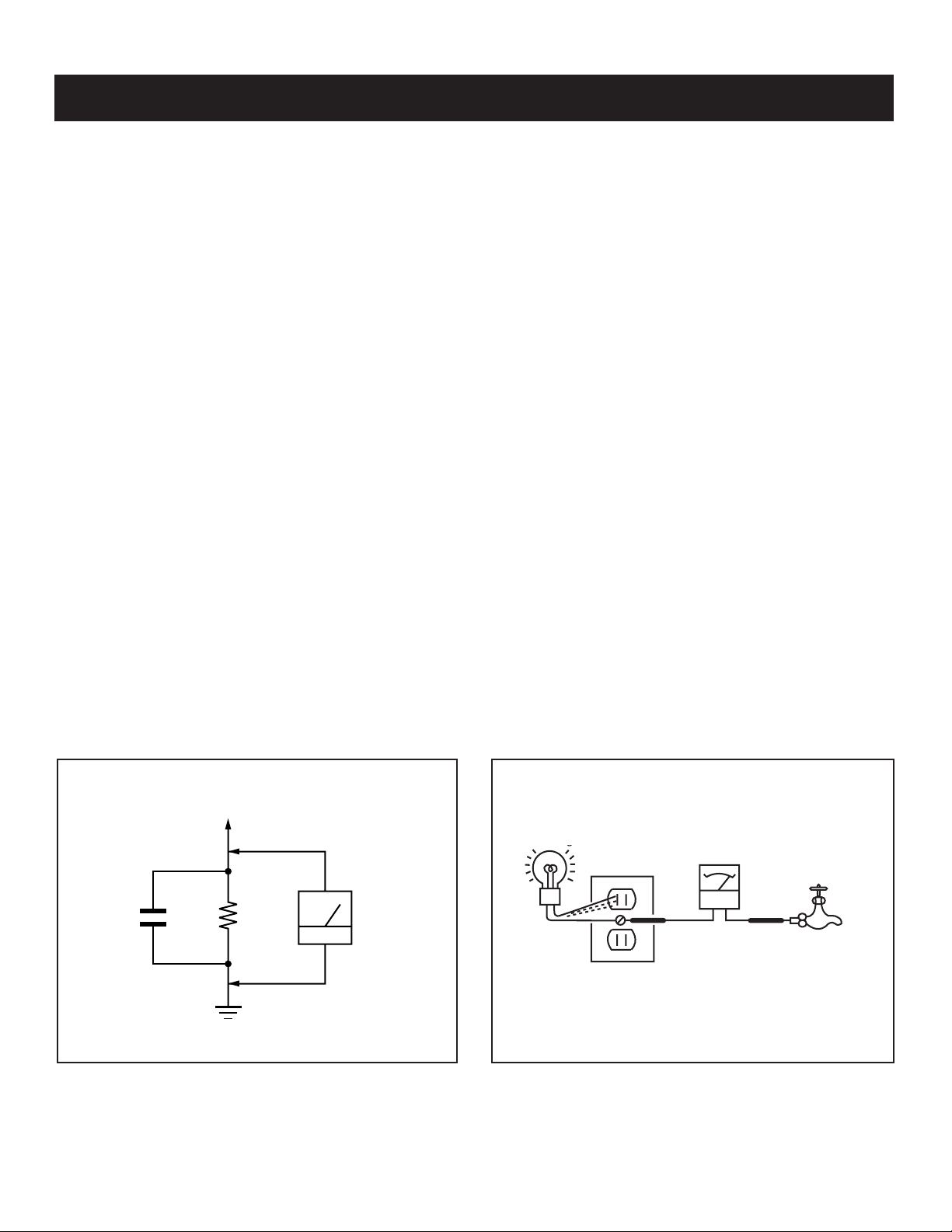
Leakage Test
The AC leakage from any exposed metal part to earth ground and from
all exposed metal parts to any exposed metal part having a return to
chassis, must not exceed 0.5 mA (500 microamperes). Leakage current
can be measured by any one of three methods.
1. A commercial leakage tester, such as the Simpson 229 or
RCA WT-540A. Follow the manufacturers’ instructions to use these
instructions.
2. A battery-operated AC milliampmeter. The Data Precision 245 digital
multimeter is suitable for this job.
3. Measuring the voltage drop across a resistor by means of a VOM
or battery-operated AC voltmeter. The “limit” indication is 0.75 V,
so analog meters must have an accurate low voltage scale. The
Simpson’s 250 and Sanwa SH-63TRD are examples of passive
VOMs that are suitable. Nearly all battery-operated digital multimeters
that have a 2 VAC range are suitable (see Figure A).
How to Find a Good Earth Ground
A cold-water pipe is a guaranteed earth ground; the cover-plate retaining
screw on most AC outlet boxes is also at earth ground. If the retaining
screw is to be used as your earth ground, verify that it is at ground
by measuring the resistance between it and a cold-water pipe with an
ohmmeter. The reading should be zero ohms.
If a cold-water pipe is not accessible, connect a 60- to 100-watt troublelight (not a neon lamp) between the hot side of the receptacle and the
retaining screw. Try both slots, if necessary, to locate the hot side on the
line; the lamp should light at normal brilliance if the screw is at ground
potential (see Figure B).
To Exposed Metal
Parts on Set
AC Outlet Box
0.15 µF
Figure A. Using an AC voltmeter to check AC leakage. Figure B. Checking for earth ground.
1.5 kΩ
Earth Ground
AC Voltmeter
(0.75 V)
Ohmmeter
Cold-water Pipe
— 6 —
KV-27FV300/29FV300/32FV300/36FV300
SELF-DIAGNOSTIC FUNCTION
Self Diagnosis
Supported model
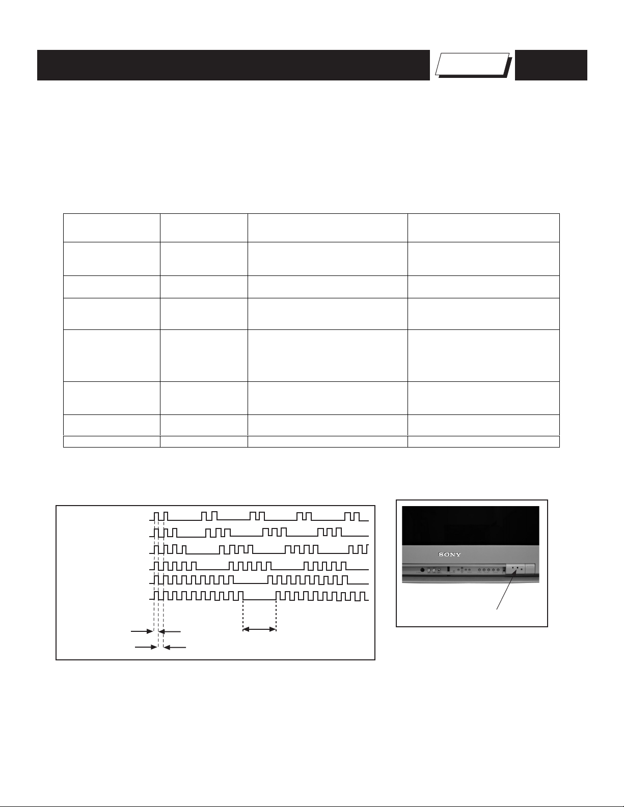
The units in this manual contain a self-diagnostic function. If an error occurs, the STANDBY/TIMER LED will automatically begin to fl ash. The number
of times the LED fl ashes translates to a probable source of the problem. A defi nition of the STANDBY/TIMER LED fl ash indicators is listed in the
instruction manual for the user’s knowledge and reference. If an error symptom cannot be reproduced, the Remote Commander can be used to review
the failure occurrence data stored in memory to reveal past problems and how often these problems occur.
Diagnostic Test Indicators
When an error occurs, the STANDBY/TIMER LED will fl ash a set number of times to indicate the possible cause of the problem. If there is more than
one error, the LED will identify the fi rst of the problem areas.
Results for all of the following diagnostic items are displayed on screen. If the screen displays a “0”, an error has occurred.
Diagnostic Item
Power does not turn on Does not light
+B overcurrent (OCP)* 2 times
+B overvoltage (OVP) 3 times
I-Prot 4 times
IK (AKB) 5 times
Zero Cross 9 times
9V Check 10 times
No. of times
STANDBY / TIMER
lamp flashes
Probable Cause Location Detected Symptoms
• Power cord is not plugged in.
• Fuse is burned out (F601). (GK Board)
• H.OUT (Q502) is shorted. (A Board)
• IC702 is shorted. (C Board)
• IC501 is faulty. (A Board)
• Ifahighissuppliedtopin2ofIC501.
(A Board)
• +12V is not supplied. (A Board)
• IC561 is faulty. (A Board)
• Video OUT (IC561) is faulty. (A Board)
• IC702 is faulty. (C Board)
• Screen (G2) is improperly adjusted. **
• No zero cross pulses on pin 45
IC1001. (A Board)
• Relay failed (RY600) • Power does not come on.
• Power does not come on.
• No power is supplied to the TV.
• AC Power supply is faulty.
• Power does not come on.
• Load on power line shorted.
• Has entered standby mode.
• Has entered standby state after
horizontal raster.
• Vertical deflection pulse is stopped.
• Power line is shorted or power
supply is stopped.
• No raster is generated.
• CRT Cathode current detection
reference pulse output is small.
• Power does not come on.
* If a +B overcurrent is detected, stoppage of the vertical deflection is detected simultaneously. The symptom that is diagnosed first
by the microcontroller is displayed on the screen.
** Refer to Screen (G2) Adjustments in Section 2-4 of this manual
Display of Standby/Timer LED Flash Count
2 times
3 times
4 times
5 times
9 times
10 times
LED ON 0.3 sec.
LED OFF 0.3 sec.
Diagnostic Item Flash Count*
+B Overcurrent 2 times
+B Overvoltage 3 times
V-STOP 4 times
IK (AKB) 5 times
Zero Cross 9 times
9V 10 times
Standby/Timer LED
LED OFF
3 sec.
*One fl ash count is not used for self-diagnostic.
— 7 —
KV-27FV300/29FV300/32FV300/36FV300
Stopping the Standby/Timer LED Flash
Turn off the power switch on the TV main unit or unplug the power cord from the outlet to stop the STANDBY/TIMER LAMP from fl ashing.
Self-Diagnostic Screen Display
For errors with symptoms such as “power sometimes shuts off” or “screen sometimes goes out” that cannot be confi rmed, it is possible to bring up
past occurrences of failure on the screen for confi rmation.
To Bring Up Screen Test
In standby mode, press buttons on the Remote Commander sequentially, in rapid succession, as shown below:
DISPLAY
SELF DIAGNOSIS
2: +B OCP 0
3: +B OVP 0
4: VSTOP 0
5: AKB 1
9: ZCD 0
10: 9VON 0
101: WDT 0
Serial: xxxxxxx
Model: xxxxxxx
Handling of Self-Diagnostic Screen Display
Since the diagnostic results displayed on the screen are not automatically cleared, always check the self-diagnostic screen during repairs. When you
have completed the repairs, clear the result display to “0”.
Unless the result display is cleared to “0”, the self-diagnostic function will not be able to detect subsequent faults after completion of the repairs.
Clearing the Result Display
To clear the result display to “0”, press buttons on the Remote Commander sequentially when the diagnostic screen is displayed, as shown below:
Quitting the Self-Diagnostic Screen
To quit the entire self-diagnostic screen, turn off the power switch on the Remote Commander or the main unit.
Numeral “0” means that no fault was detected.
Numeral “1” means a fault was detected one time only.
8
ENTERChannel
Channel 5 Sound volume - Power ON.
Self-Diagnostic Circuit
Y/CHROMA JUNGLE
FROM
C BOARD
IC702 PIN 5
A BOARD
FROM
Q530
36
33
A BOARD
IC301
IK-AKBIN
VM-OUT
HP(HLDWN)
SDA
TO V BOARD
Q904
BASE
31
A BOARD
Q651
61
A BOARD
IC561
V. OUT
REF
3
— 8 —
FROM
A BOARD
Q003
COLLECTOR
A BOARD
IC001
SYSTEM
IO-BDAT
48
I-OCP
27
O-LED
26
59
A BOARD
IC003
MEMORY
5
BDA
DISPLAY

KV-27FV300/29FV300/32FV300/36FV300
+B overcurrent (OCP)
Occurs when an overcurrent on the +B (135V) line is detected by pin 48 of IC001 (A Board). If the voltage of pin 48 of IC001 (A Board) is less than 1V
when V.SYNC is more than seven verticals in a period, the unit will automatically turn off.
+B overvoltage (OVP)
Occurs when a high is felt onpin 2 of IC501 (A Board).
I-PROT
Occurs when an absence of the vertical defl ection pulse is detected by pin 31 of IC301 (A Board). Power supply will shut down when waveform
interval exceeds 2 seconds.
IK (AKB)
If the RGB levels* do not balance within 2 seconds after the power is turned on, this error will be detected by IC301 (A Board). TV will stay on,
but there will be no picture.
*(Refers to the RGB levels of the AKB detection Ref pulse that detects 1K).
Zero Cross
Check Q691 collector (GK Board) 7.5V STBY goes to 0V when the set is turned on.
9V Check
Check Q691 collector (GK Board) 7.5V STBY goes to 0V when the set is turned on.
— 9 —
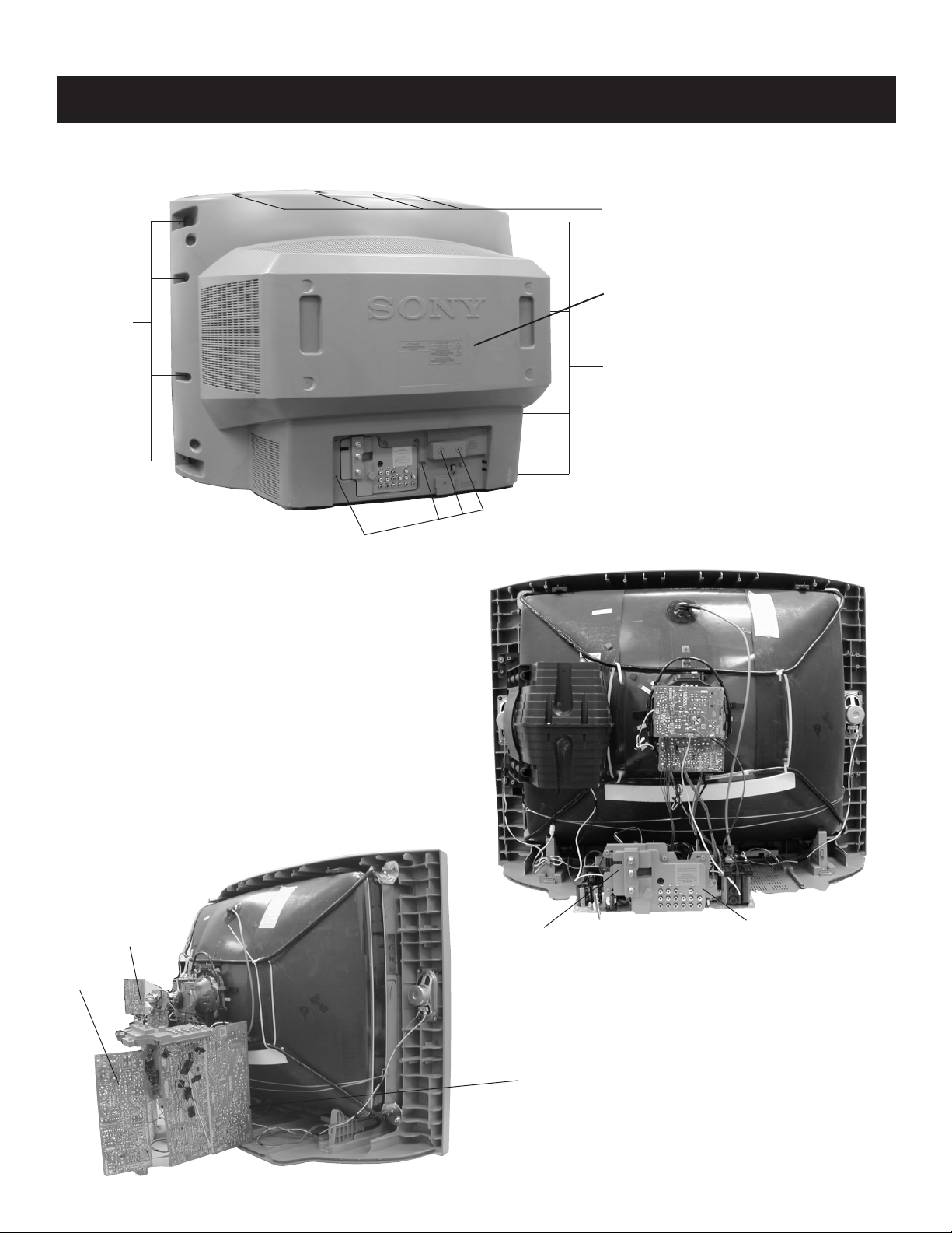
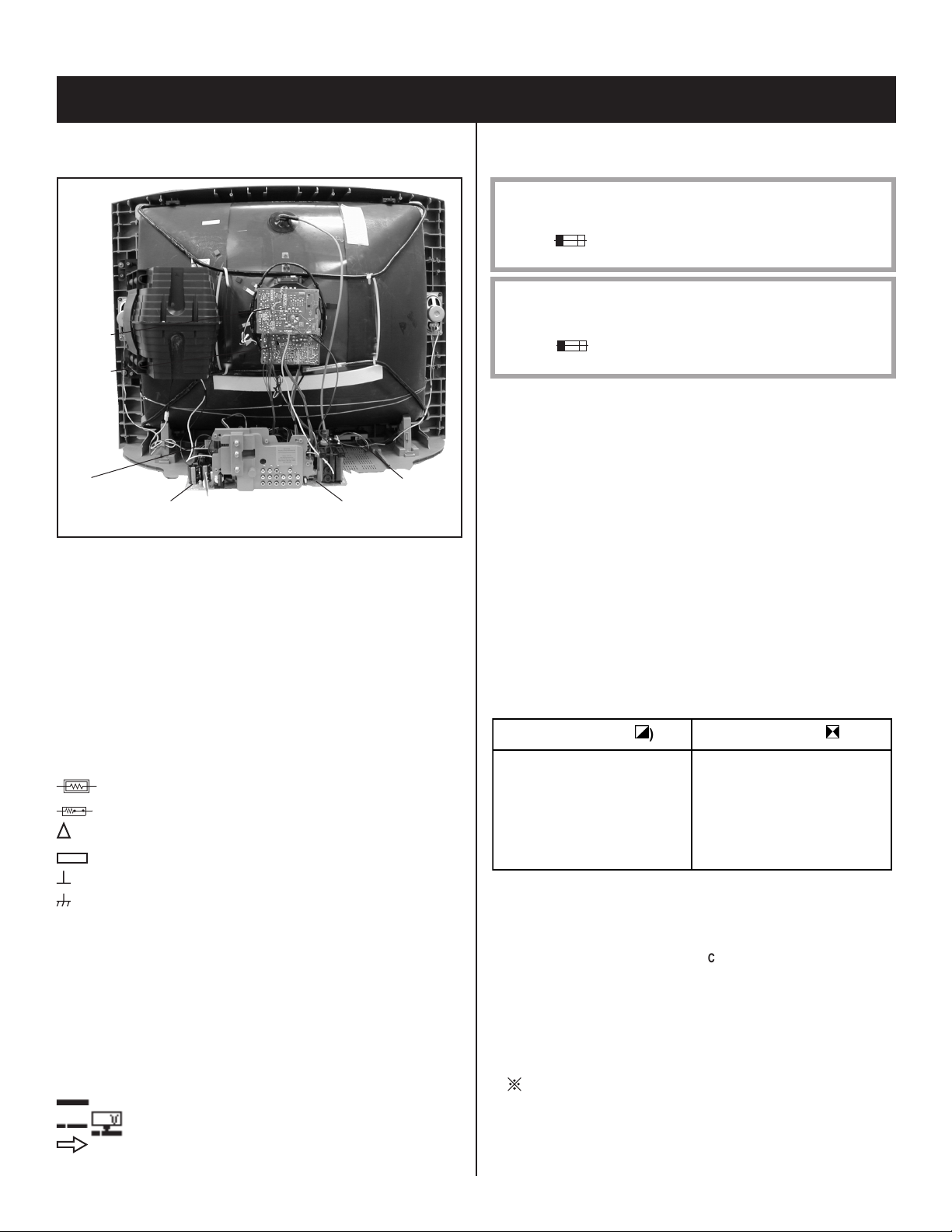
1-1. REAR COVER REMOVAL
4 Screws
+BVTP 4 x 16
KV-27FV300/29FV300/32FV300/36FV300
SECTION 1: DISASSEMBLY
4 Screws
+BVTP 4 x 16
Rear Cover
4 Screws
+BVTP 4 x 16
1-3. SERVICE POSITION
C Board
GK Board
7 Screws
+BVTP 4 x 16
1-2. CHASSIS ASSEMBLY REMOVAL
Claw Chassis Assembly
— 10 —
A Board
1-4. PICTURE TUBE REMOVAL
WARNING: BEFORE REMOVING THE ANODE CAP
High voltage remains in the CRT even after the power is disconnected. To avoid electric shock,
discharge CRT before attempting to remove the anode cap. Short between anode and CRT
coated earth ground strap.
11
9
3
7
10
1
2
1. Discharge the anode of the CRT and remove the anode cap.
2. Unplug all interconnecting leads from the defl ection yoke,
neck assembly, degaussing coils and CRT grounding strap.
4
8
3. Remove the Sub-Woofer Assemblies.
4. Remove the C Board from the CRT.
5. Remove the chassis assembly.
6
6. Loosen the neck assembly fi xing screw and remove.
7. Loosen the defl ection yoke fi xing screw and remove.
8. Place the set with the CRT face down on a cushion and
remove the degaussing coil holders.
9. Remove the degaussing coils.
10. Remove the CRT grounding strap and spring tension devices.
11. Unscrew the four CRT fi xing screws [located on each CRT
corner] and remove the CRT [Take care not to handle the
CRT by the neck].
KV-27FV300/29FV300/32FV300/36FV300
Coated
Earth
Ground
Strap
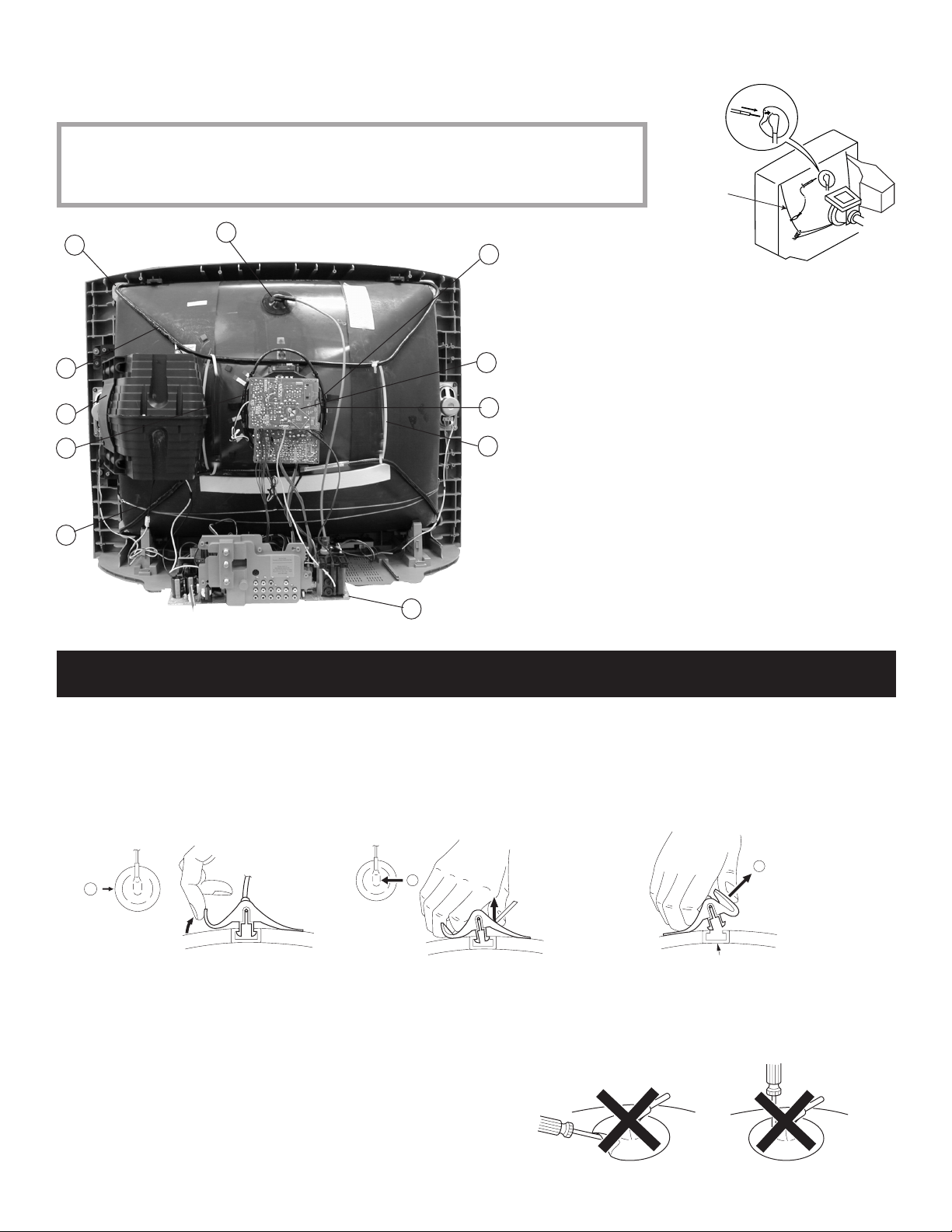
5
ANODE CAP REMOVAL PROCEDURE
WARNING: High voltage remains in the CRT even after the power is disconnected. To avoid electric shock, discharge CRT before attempting to remove
the anode cap. After removing the anode cap, short circuit to either the metal chassis, CRT shield, or carbon painted on the CRT.
NOTE: After removing the anode cap, short circuit the anode of the picture tube and the anode cap to either the metal chassis, CRT shield or
carbon painted on the CRT.
REMOVAL PROCEDURES
c
a
Turn up one side of the rubber cap in
the direction indicated by arrow a .
HOW TO HANDLE AN ANODE CAP
b
Use your thumb to pull the rubber
cap fi rmly in the direction indicated
by arrow b .
Anode Button
When one side of the rubber cap separates from
the anode button, the anode cap can be removed
by turning the rubber cap and pulling it in the
direction of arrow c .
1. Do not use sharp objects which may cause damage to the surface of the anode
cap.
2. To avoid damaging the anode cap, do not squeeze the rubber covering too hard.
A material fi tting called a shatter-hook terminal is built into the rubber.
3. Do not force turn the foot of the rubber cover. This may cause the shatter-hook
terminal to protrude and damage the rubber.
— 11 —
SECTION 2: SET-UP ADJUSTMENTS
KV-27FV300/29FV300/32FV300/36FV300
The following adjustments should be made when a complete
realignment is required or a new picture tube is installed.
These adjustments should be performed with rated power supply
voltage unless otherwise noted.
The controls and switch should be set as follows unless otherwise
noted:
PICTURE CONTROL: normal
BRIGHTNESS CONTROL: normal
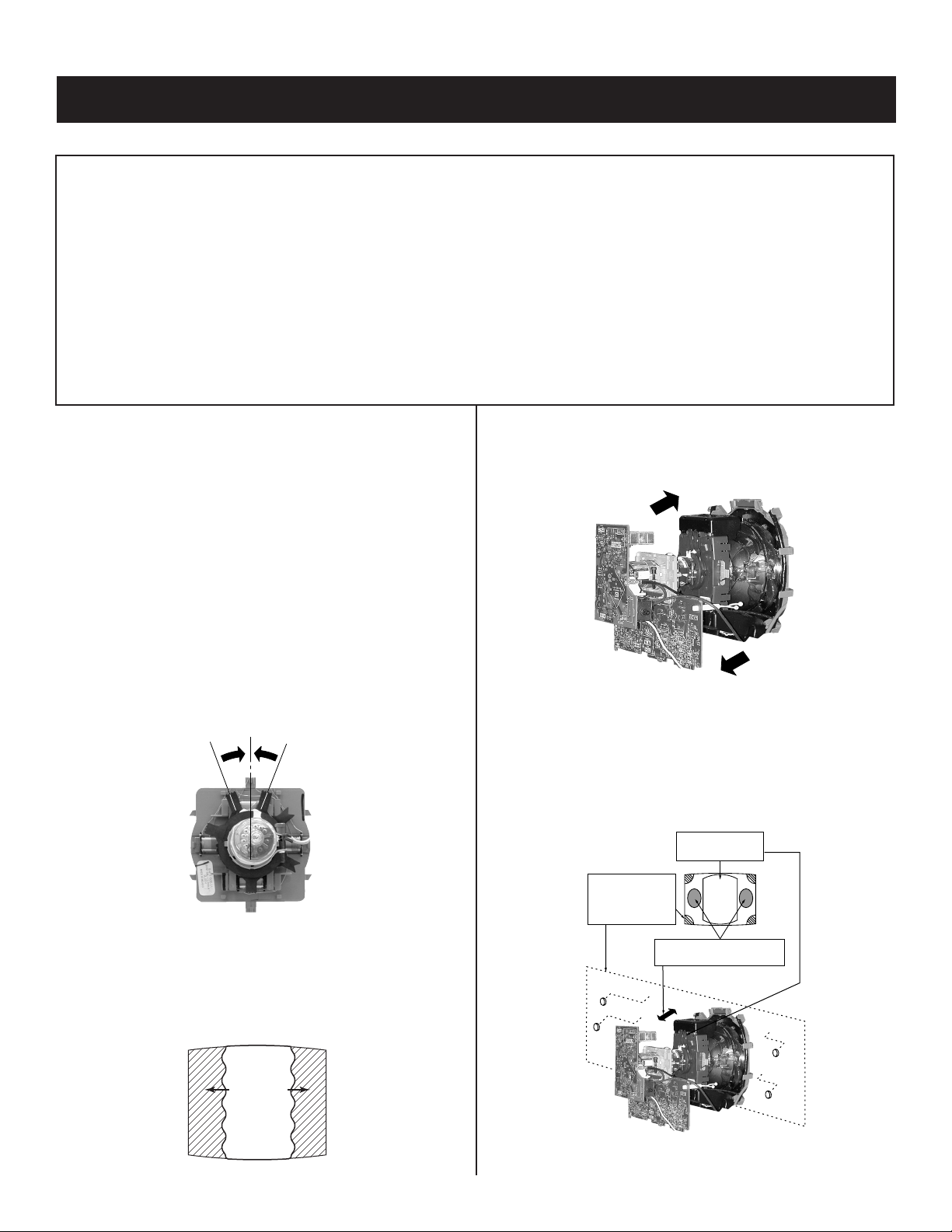
2-1. BEAM LANDING
Preparation:
• Input a white pattern signal.
• Face the picture tube in an East or West direction to reduce the
infl uence of geomagnetism.
NOTE: Do not use the hand degausser; it magnetizes the CRT .
1. Input white pattern from pattern generator.
2. Loosen the defl ection yoke mounting screw, and set the purity control
to the center as shown below:
Perform the adjustments in order as follows:
1. Beam Landing
2. Convergence
3. Focus
4. Screen (G2)/White Balance
Test Equipment Required:
1. Color Bar Pattern Generator
2. Degausser
3. DC Power Supply
4. Digital Multimeter
5. Oscilloscope
6. CRT Analyzer
5. Move the defl ection yoke forward, and adjust so that the entire screen
becomes green.
Purity Control
3. Input green pattern from pattern generator.
4. Move the defl ection yoke backward, and adjust with the purity control
so that green is in the center and red and blue are even on both
sides.
Blue Red
Green
6. Switch over the raster signal to red and blue and confi rm the
condition.
7. When the position of the defl ection yoke is determined, tighten it with
the defl ection yoke mounting screw.
8. When landing at the corner is not right, adjust by using the disk
magnets.
Purity control
corrects this area
Disk magnets
or rotatable disk
magnets correct
these areas (a-d)
b
d
cd
Deflection yoke positioning
corrects these areas
ba
a
c
— 12 —
KV-27FV300/29FV300/32FV300/36FV300
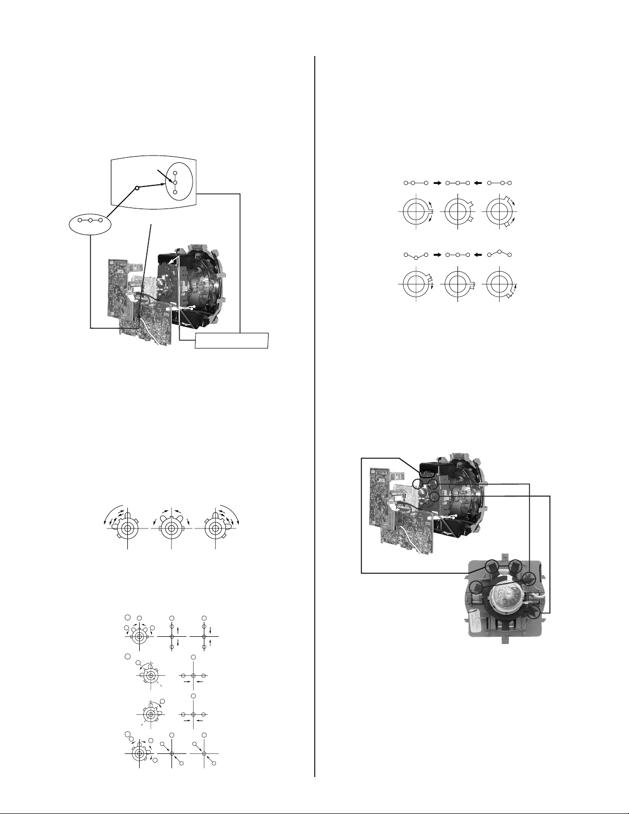
2-2. CONVERGENCE
Preparation:
• Perform FOCUS, V. LIN and V. SIZE adjustments.
• Set BRIGHTNESS control to minimum.
• Input dot pattern.
Center dot
RV701 V.STAT
R G B
R
G
B
V.STAT magnet
OPERATION OF BMC (HEXAPOLE) MAGNET
The respective dot positions resulting from moving each magnet interact,
so perform adjustment while tracking.
1 Use the V.STAT tabs to adjust the red, green, and blue dots so they
line up at the center of the screen (move the dots in a horizontal
direction).
RG B
RGB RGB
RGB
RGB
RGB
Y SEPARATION AXIS CORRECTION MAGNET
ADJUSTMENT
VERTICAL AND HORIZONTAL STATIC
CONVERGENCE
1. Adjust V. STAT magnet to converge red, green and blue dots in the
center of the screen (Vertical movement).
Tilt the V. STAT magnet and adjust static convergence to open or
close the V. STAT magnet.
2. When the V. STAT magnet is moved in the direction of arrow a and b,
red, green, and blue dots move as shown below:
1
a
b
2
a
a
B
b
G
R
B
G
R
a
RG B
b
1. Input cross-hatch pattern, adjust PICTURE to minimum and
BRIGHTNESS to normal.
2. Adjust the defl ection yoke upright so it touches the CRT.
3. Adjust so that the Y separation axis correction magnet on the neck
assembly is symmetrical from top to bottom (open state).
V. STAT
BMC MAGNET
PURITY
4. Return the defl ection yoke to its original position.
a
G
BG R
B
B
b
b
G
R
b
3
b
a
R
b
— 13 —
KV-27FV300/29FV300/32FV300/36FV300
DYNAMIC CONVERGENCE ADJUSTMENT
Before starting, perform Vertical and Horizontal Static Convergence
Adjustment.
1. Slightly loosen defl ection yoke screw.
2. Remove defl ection yoke spacers.
3. Move the defl ection yoke for best convergence as
shown below:
BGR
R
B
G
G
R
B
B
G
R
RGB
RGB
G
B
BGR RGB
R
G
B
R
RGB
BGR
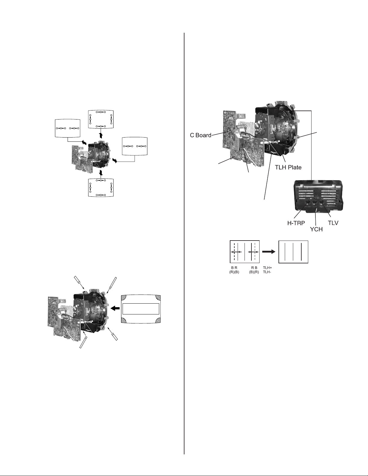
TLH PLATE ADJUSTMENT
Preparation:
• Input crosshatch pattern.
• Adjust Picture Quality to standard, Picture and Brightness to 50%, and
Other to standard.
• Adjust the Horizontal Convergence of red and blue dots by tilting the
TLH plate on the defl ection yoke.
Y Magnet
WA Board
RV701
V. STAT
XCV
4. Tighten the defl ection yoke screw.
5. Install the defl ection yoke spacers.
SCREEN-CORNER CONVERGENCE
1. Affi x a permalloy assembly corresponding to the misconverged areas:
b
a
1. Adjust XCV core to balance X axis.
ba
a-d: screen-corner
misconvergence
cd
c
d
2. Adjust YCH VR to balance Y axis.
3. Adjust vertical red and blue convergence with V.TILT (TLV VR.)
4. Adjust Y MAGNET to correct V.BOW Geometry Distortion.
5. Adjust H-TRP to correct H.Trapezoid Geometry Distortion.
After adjusting items 4 and 5, confi rm overall geometry again.
Perform adjustments while tracking items 1 and 2.
— 14 —
KV-27FV300/29FV300/32FV300/36FV300
2-3. FOCUS
1. Input monoscope signal.
2. Set user controls to normal.
3. Set video mode to STANDARD.
4. Set the PICTURE to maximum.
5. Adjust at 325 Mark for best center/corner focus balance.
6. Receive an entire white signal. Make sure Magenta Ring is at an
acceptable level.
Focus
Screen (G2)
325 MARK
35
35 MARK
CENTER
CIRCLE
325
2-5. WHITE BALANCE ADJUSTMENTS
Adj. NO. Disp. Item All Models
VID_ADJ 0 RDRV Red Drive 41
VID_ADJ 1 GDRV Green Drive 32
VID_ADJ 2 BDRV Blue Drive 29
VID_ADJ 3 RCUT Red Cut-off 31
VID_ADJ 4 GCUT Green Cut-off 14
VID_ADJ 5 BCUT Blue Cut-off 17
VP2 4 SBRT Sub Bright 16
1. Set program palette to STANDARD and push RESET.
2. Input an entire white signal.
3. Set to Service Adjustment Mode.
4. Set the PICTURE and BRIGHT to minimum.
5. Adjust with SBRT if necessary.
6. Set RCUT to “14”.
7. Select GCUT and BCUT with
8. Adjust by pressing
1
and
9. Set the PICTURE and BRIGHT to maximum.
10. Select GDRV and BDRV with and .
11. Adjust with 3 and 6 for the best white balance.
12. Write into the memory by pressing
13. Repeat steps 1-12 for GDR4, BDR4, GCU4 and BCU4 using
Video 4 input.
3
and 5 .
4
for the best white balance.
5
3
then
.
2-4. SCREEN (G2)
1. Input dot pattern from the pattern generator.
2. Set the user controls to NORMAL.
3. Attach the G2-Jig to the C Board.
4. Adjust RCUT, GCUT, BCUT, and SBRT in service mode with an
oscilloscope so that voltages on the red, green, and blue cathodes
are 170 ± 2.0Vdc.
5. Observe the screen and adjust SCREEN (G2) VR to obtain the
faintly visible background of dot signal.
6. Push the TEST + JUMP (+ Channel) to cut off the signal. The screen
should be bright or dark. Brightness of raster must be increased
when adjusting.
7. Adjust screen VR until the screen is slightly cut off, or scarcely lights
up. A signal cannot be seen when the brightness of the raster is
high.
8. Push the JUMP again to release the cut off.
* Use values from Sub Contrast Adjustments
White balance should be adjusted after Sub Contrast because
RDRV is also used in Sub Contrast Adjustment. (See page 22).
170 + 2.0 Vdc
GND
170Vdc
pedestal
— 15 —
SECTION 3: SAFETY RELATED ADJUSTMENTS
KV-27FV300/29FV300/32FV300/36FV300
3-1. X R530, R531 CONFIRMATION METHOD
(HOLD-DOWN CONFIRMATION) AND
READJUSTMENTS
Always perform the following adjustments when replacing the following
components marked with a
Y
mark on the schematic diagram:
Part Replaced () Adjustment ()
A BOARD: HV HOLD DOWN
R550, T503, T504, D519,
R530, R531
IC501, R533, D521, R532,
D520, C531, R529, R530,
R531, C532
PREPARATION BEFORE CONFIRMATION
1. Using a Variac, apply AC input voltage: 120+2.0 VAC.
2. Turn the POWER switch ON.
3. Input a white signal and set the PICTURE and BRIGHT controls to
maximum.
4. Confi rm that the voltage of more than 23.0 VDC appears between
TP85 and ground on the A Board.
HOLD-DOWN READJUSTMENT
If the setting indicated in Step 2 of Hold-Down Operation Confi rmation
cannot be met, readjustment should be performed by altering the
resistance value of R530, R531 component marked with
digital multimeter
+
-
T503
FBT
FBT
R531
R530
TP85
TP85
ammeter
3mA DC range
A
+
-
DC Power Supply
+
-
Figure 1
X
.
HOLD-DOWN OPERATION CONFIRMATION
1. Connect the current meter between Pin 11 of the FBT (T503) and the
PWB land where Pin 11 would normally attach. (See Figure 1).
2. Input a dot signal and set PICTURE and BRIGHTNESS to minimum:
IABL = 2175 + 100/ -325 µA.
3. Confi rm the voltage of A Board TP91 is 135 ± 1.5 VDC.
4. Connect the digital voltmeter and the DC power supply to TP85 and
ground. (See Figure 1 above).
5. Increase the DC power voltage gradually until the picture blanks out.
6. Turn DC power source off immediately.
7. Read the digital voltmeter indication (standard = 27.24 + 0.0/ - 0.1
VDC).
8. Input a white signal and set PICTURE and BRIGHTNESS to
maximum: IABL = 2175 + 100/ -325 µA.
9. Repeat steps 4 to 7.
3-2. B+ VOLTAGE CONFIRMATION AND
ADJUSTMENT
Always perform the following adjustments when replacing the following
components, which are marked with
the GK Board:
GK BOARD: IC600, PH602
1. Using a Variac, apply AC input voltage: 130 + 2.0/-0.0 VAC
2. Input a monoscope signal.
3. Set the PICTURE control and the BRIGHT control to
minimum.
4. Confi rm the voltage on A Board between TP23 and ground is less
than 136.5 VDC.
5. If step 4 is not satisfi ed, replace R530 and R531 on A Board and
repeat the above steps.
Y
on the schematic diagram on
— 16 —
SECTION 4: CIRCUIT ADJUSTMENTS
ELECTRICAL ADJUSTMENTS BY REMOTE COMMANDER
Use the Remote Commander (RM-Y181, RM-Y182) to perform the circuit adjustments in this section.
Test Equipment Required: 1. Pattern generator 2. Frequency counter 3. Digital multimeter 4. Audio oscillator
KV-27FV300/29FV300/32FV300/36FV300
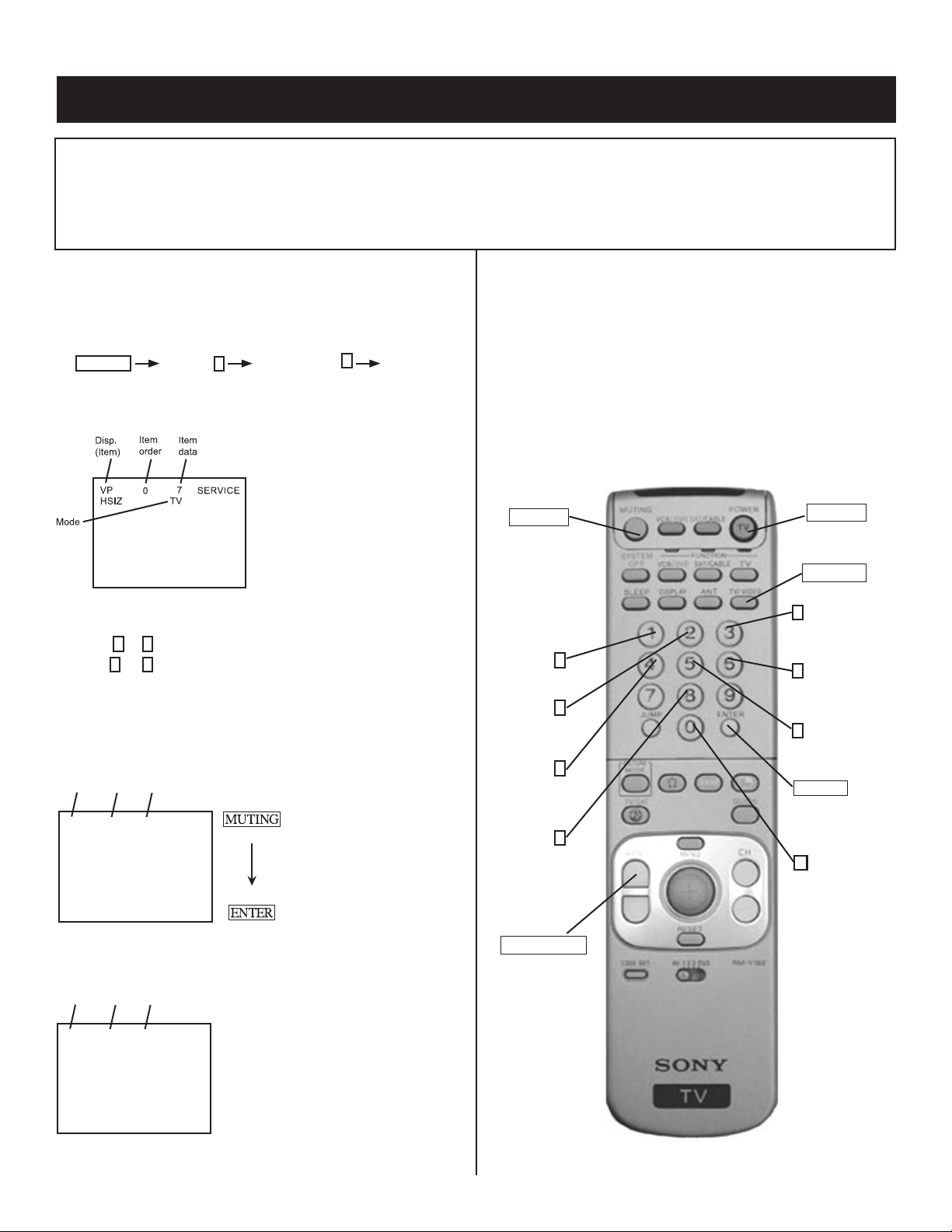
4-1. SETTING SERVICE ADJUSTMENT MODE
1. Standby mode (Power off).
2. Press the following buttons on the remote commander within a
second of each other:
DISPLAY
Channel 5 Sound Volume
+
Power
SERVICE ADJUSTMENT MODE IN
3. The CRT displays the item being adjusted.
4. Press
5. Press
1
or 2 on the Remote Commander to select the item.
3
or 6 on the Remote Commander to change the data.
6. Press MUTING then ENTER to write into memory.
SERVICE ADJUSTMENT MODE MEMORY
Item
order
0
TV
Item
data
7
SERVICE
Green
Red
Disp.
(Item)
VP
HSIZ
4-2. MEMORY WRITE CONFIRMATION
METHOD
1. After adjustment, pull out the plug from the AC outlet, then replace
the plug in the AC outlet again.
2. Turn the power switch ON and set to Service Mode.
3. Call the adjusted items again to confi rm they were adjusted.
4-3. REMOTE ADJUSTMENT BUTTONS AND
INDICATORS
MUTING
(Enter into
memory)
1
Disp. (Item up)
2
(Device Item Up)
4
Disp. (Item down)
8
(Initialize)
POWER
(Service Mode)
DISPLAY
(Service Mode)
3
Item
(Data up)
6
Item
(Data down)
5
(Device item
down)
ENTER
(Enter into
memory)
0
(Remove from
memory)
7. Press then on the Remote Commander to initialize.
Item
order
0
TV
Item
data
7
WRITE
Disp.
(Item)
VP
HSIZ
8. DO NOT turn off set until SERVICE appears.
VOLUME (+)
(Service Mode)
RM-Y182
— 17 —
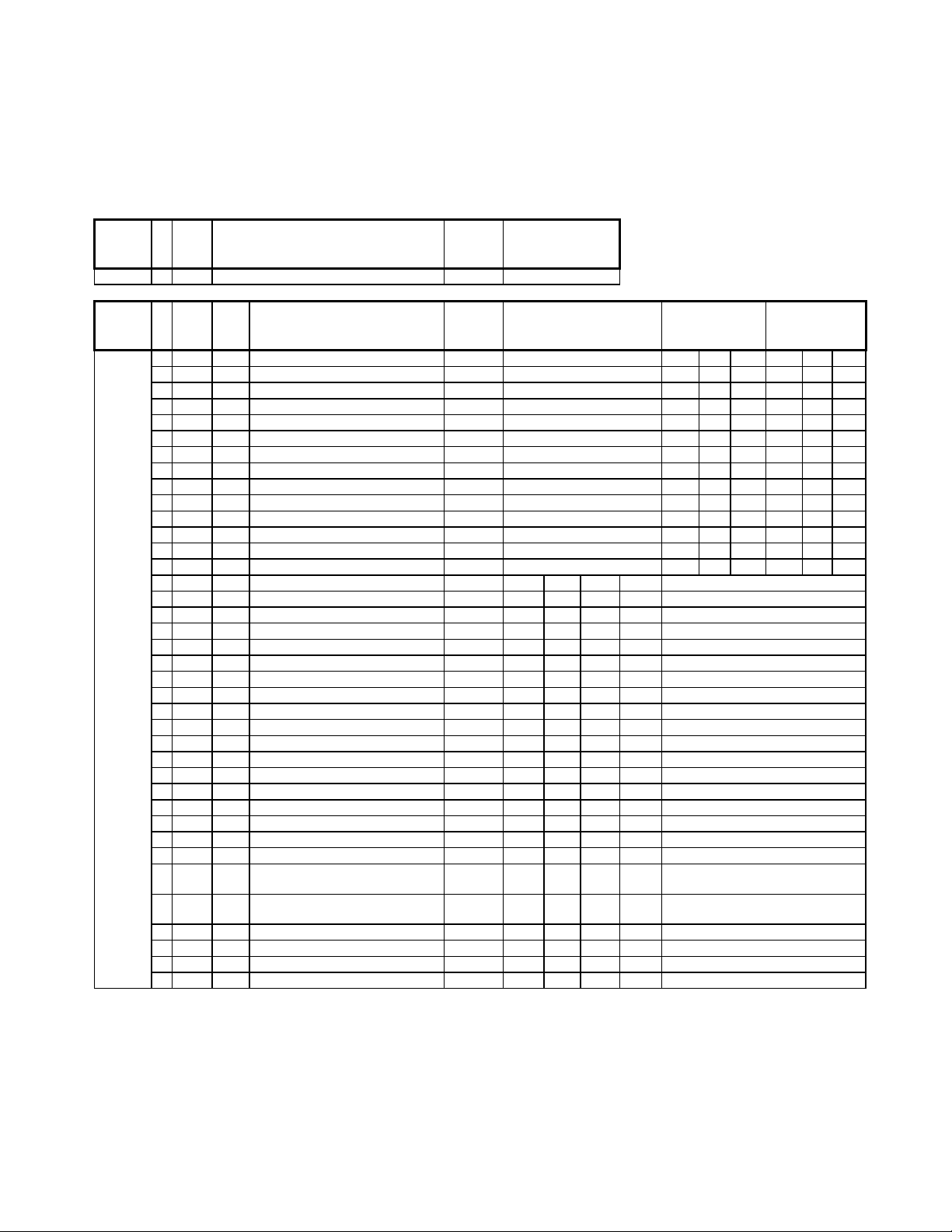
SERVICE DATA LISTS4-4.
Non-Volatile Memory (NVM) Reference for BA5D Service List
KV-27FV300/29FV300/32FV300/36FV300
Service
VERSION 0 VER 11111111 = = 0
Service
No. Name Bit Mask
Group
Microprocessor version information
Name
Fix /
Var
Vertical Count Down Mode Switching (for
TV)
Vertical Count Down Mode Switching (for
Video)
No.
Group
VP1 0 HSIZ Var H SIZE (11/ 2-7) 11111100 A4 A8 A4 B4
1 HPOS Var HPOS (12 / 2-7) 11111100 A4 A9 A4 B5
2 VBOW Var AFC BOW (16 / 4-7) 11110000 A4 AE A4 BA
3 VANG Var AFC ANGLE (16 / 0-3) 00001111 A4 AE A4 BA
4 VTRP Var TRAPEZIUM (20 / 3-7) 11111000 A4 AF A4 BB
5 HTRP Var H. TRAPEZOID (15 / 4-7) 11110000 A4 AD A4 B9
6 TROT Fix TILT ROTATION (0-63) 11111100 A4 A4 A4 B0
7 PAMP Var PIN AMP (13 / 2-7) 11111100 A4 AA A4 B6
8 UPIN Var UP-CPIN (14 / 2-7) 11111100 A4 AB A4 B7
9 LPIN Var LO-CPIN (1C / 2-7) 11111100 A4 AC A4 B8
10 VSIZ Var V SIZE (0E / 2-7) 11111100 A4 A5 A4 B1
11 VPOS Var V POSITION (0E / 2-7) 11111100 A4 A6 A4 B2
12 VLIN Var V LINEARITY (10 / 0-3) 00001111 A4 A7 A4 B3
13 SCOR Var S CORRECTION (10 / 4-7) 11110000 A4 A7 A4 B3
14 VZOM Fix 16:9 CRT Z Mode on/off 10000000 A4 85
15 EHT Fix Vertical High-Voltage Compensation 00001111 A4 80
16 ASP Fix Aspect Ratio control (4:3 Mode) 11111100 A4 FB 47
17 ASP1 Fix Aspect Ratio control (16:9 Mode) 11111100 A4 FC 47
18 SCRL Fix 16:9 CRT Z Mode Trans. Scroll 00111111 A4 86
19 HBLK Fix Horizontal Blanking on/off 00010000 A4 85
20 LBLK Fix Left Blanking Adjustment 11110000 A4 80
21 RBLK Fix Rigth Blanking Adjustment 00001111 A4 81
22 HDW Fix Horizontal Drive Pulse Width 00001000 A4 85
23 EWDC Fix "Parabola" EW, D.C. Adjustment 00000100 A4 88
24 LVLN Fix Lower Screen BTM Vertical Line Adj. 11110000 A4 81
25 UVLN Fix Uppe Screen BTM Vertical Line Adj. 00001111 A4 82
26 INTL Fix INTERLACE 00110000 A4 84
27 HOSC Fix Horizontal VCO Oscillation Freq. 11110000 A4 82
28 VSS Fix Vertical Sync Slice Level 11000000 A4 84
29 HSS Fix Horizontal Sync Slice Level 00001000 A4 88
30 HMSK Fix For Macro Vision 00010000 A4 88
31 VTMS Fix Select Signal VTIM Pin 01100000 A4 85
32 TCMD Fix
33 VCMD Fix
34 AFC Fix AFC Loop Gain Switching 11000000 A4 86
35 FIFR Fix Field Frequency 11000000 A4 87
36 VBLK Fix VBLKW 00000011 A4 88
37 HTSW Fix H-Trap Switch : NEW 00100000 A4 88
Description
Description Bit Mask
00000011 A4 8C
00000011 A4 8D
Common
Slave Sub Init
Addr Addr Data
Slave Sub Fix Var Slave Sub Slave Sub
Addr Addr Data Data Addr Addr Data Addr Addr Data
PAL-NNTSC / PAL-MCommon
— 18 —
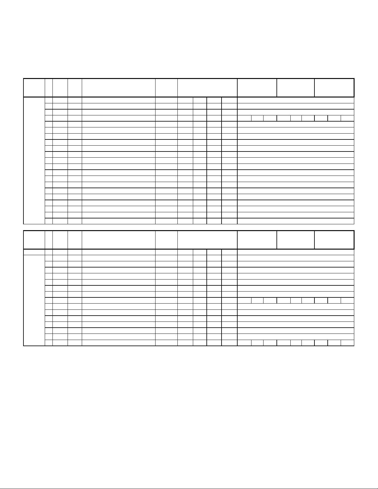
SERVICE DATA LISTS
KV-27FV300/29FV300/32FV300/36FV300
Service
No. Name
Group
VP2 0 REFP Fix REFP 01000000 A4 88 0
1 JPSW Fix Jump SW 00000001 = =
2 SHUE Var Sub HUE adjustment 11110000 A4 8C
3 SCOL Var Sub COLOR adjustment 00001111 A4 8E A4 90 7 A4 92
4 SBRT Var Sub BRIGHTNESS adjustment 00011111 A4 87
5 AXPL Fix Axis PAL 00000001 A4 89 0
6 AXNT Fix Axis NTSC 00000010 A4 89 1
7 CBPF Fix Chroma BPF on/off 00000100 A4 89 1
8 CTRP Fix Y TRAP FILTER on/off 00000001 = =
9 COFF Fix Color On/off 00000010 = =
10 KOFF Fix Set Color Killer 00100000 A4 89 0
11 SSHP Fix Sub SHARPNESS 11110000 A4 83
12 TSPF Fix SHARPNESS Circuit Fo (for TV) 00001100 A4 8C
13 VSPF Fix SHARPNESS Circuit Fo (for Video) 00001100 A4 8D
14 PREL Fix Pre-Shoot/ Over-Shoot 01000000 A4 89 1
15 ABLM Fix ABL Mode Switch 10000000 A4 89 1
16 VTH Fix ABL CD VHT Switching 00000001 = =
17 YDEL Fix Y Delay Time Control 00001111 A4 84
18 NCOL Fix No Color ID 00000001 A4 85
19 FSC Fix FSC Out on/off 00000010 A4 85 1
20 KID Fix Killer ID Control on/off 00000100 A4 85 0
Service
No. Name
Group
VID_ADJ 0 RDRV var R DRIVE (0A / 7-2) 11111100 A4 9E 41
1 GDRV Var G DRIVE (0B / 7-2) 11111100 A4 9F
2 BDRV Var B DRIVE (0C / 7-2) 11111100 A4 A0
3 RCUT Var R CUT OFF ( 07 / 7-2) 11111100 A4 A1 31
4 GCUT Var G CUT OFF (08 / 7-2) 11111100 A4 A2
5 BCUT Var B CUT OFF (09 / 7-2) 11111100 A4 A3
6 SCON Var Sub Contrast adjusment 00001111 A4 8A
7 CHUE Var Sub HUE adjustment for TV 00011111 A4 94 16
8 CCOL Var Sub COLOR adjustment for TV 00011111 A4 8F 18 A4 91 18 A4 93 23
9 UOFS Var YUV U offset 00001111 A4 8B
10 VOFS Var YUV V offset 11110000 A4 8B
11 RON Fix R ON (01 / 3) 00001000 = =
12 GON Fix G ON (01 / 2) 00000100 = =
13 BON Fix B ON (01 / 1) 00000010 = =
14 HUEV Var Sub HUE adjustment for Video 11110000 A4 8D
15 COLV Var Sub COLOR adjustment for Video 11110000 A4 8E A4 90 A4 92
Fix /
Var
Fix /
Var
Description Bit Mask
Description Bit Mask
Slave Sub Fix Var Slave Sub Slave Sub Slave Sub
Addr Addr Data Data Addr Addr Data Addr Addr Data Addr Addr Data
Slave Sub Fix Var Slave Sub Slave Sub Slave Sub
Addr Addr Data Data Addr Addr Data Addr Addr Data Addr Addr Data
PAL-NCommon NTSC PAL-M
NTSC PAL-M PAL-NCommon
— 19 —
SERVICE DATA LISTS
KV-27FV300/29FV300/32FV300/36FV300
Service
No. Name
Group
COL_TMP 0 GDOF Fix G DRIVE Offset 11111000 A4 9A 4
Service
Group
PIC_IMP 0 BLAD Fix Black area detect (01 / 6-7) 11000000 A4 09 0
1 BDOF Fix B DRIVE Offset 11111000 A4 9B 15
2 GCOF Fix G CUT Offset 11111000 A4 9C 7
3 BCOF Fix B CUT Offset 11111000 A4 9D 14
4 DCOL Fix Dinamic Color 00000010 = =
No. Name
1 SRTS Fix SRT level (01 / 4-5) 00110000 A4 09 3
2 YNR Fix YNR(01 / 2) 00000100 A4 09 1
3 GIRE Fix Gamma correction(01 / 0-1) 00000011 A4 09 3
4 DAC1 Fix DAC1(02 / 7) 10000000 A4 0A 0
5 DAC2 Fix DAC2(02 / 6) 01000000 A4 0A 0
6 VMGA Fix VM on 1226 (02/5-4) 00110000 A4 0A 0
7 GCUR Fix Gamma curve(02 / 2) 00000100 A4 0A 1
8 BLKC Fix Black Compensation (02 / 1) 00000010 A4 0A 1
9 TEST Fix TEST(03 / 6-7) 11000000 A4 0B 3
10 RS Fix RS (03 / 3-5) 00111000 A4 0B 0
11 RTC Fix RTC(03 / 0-2) 00000111 A4 0B 2
12 APAC Fix APAC 10000000 A4 0B 0
13 SRTH Fix SRT bit for Dynablack = High 10000000 A4 5C 1
14 SRTL Fix SRT bit for Dynablack = Low 10000000 A4 5D 1
15 SRTO Fix SRT bit for Dynablack = Off 10000000 A4 5E 0
16 SHPH Fix Sharpness level for Dynablack = High 01111111 A4 5C 54
17 SHPL Fix Sharpness level for Dynablack = Low 01111111 A4 5D 43
18 SHPO Fix Sharpness level for Dynablack = Off 01111111 A4 5E 0
Fix /
Var
Fix /
Var
Description Bit Mask
Description Bit Mask
Common
Slave Sub Fix
Addr Addr Data
Common
Slave Sub Fix
Addr Addr Data
Service
No. Name
Group
PALETTE 0 VPIC Fix User picture setting 0:min, 63: max 11111100 A4 5F 63 A4 65 50 A4 6B 38 A4 71 63
1 VBRT Fix User brightness setting 0:min, 63: max 11111100 A4 60 31 A4 66 31 A4 6C 31 A4 72 31
2 VCOL Fix User color setting 0:min, 63: max 11111100 A4 61 35 A4 67 31 A4 6D 31 A4 73 40
3 VSHP Fix User sharpness setting 0:min, 63: max 11111100 A4 62 31 A4 68 31 A4 6E 34 A4 74 31
4 VVM Fix 0: OFF, 1: Low, 2: High, 3: N/A 00000011 A4 5F 2 A4 65 1 A4 6B 0 A4 71 2
5 VTRI Fix 0: Cool, 1: Nutral, 2: Warm, 3: N/A 00000011 A4 60 0 A4 66 1 A4 6C 2 A4 72 0
6 VGMA Fix 0: OFF, 1: Low, 2: Mid, 3: Max 00000011 A4 63 2 A4 69 2 A4 6F 2 A4 75 2
7 VNRM Fix 0: 3D, 1: 2D 00000010 A4 61 0 A4 67 0 A4 6D 0 A4 73 0
8 VYDC Fix
9 VVEN Fix Vertoca; Enhancement 00011100 A4 63 5 A4 69 3 A4 6F 3 A4 75 5
10 VHK0 Fix Horizontal Peaking 0:On, 1:Off 00000001 A4 61 0 A4 67 0 A4 6D 0 A4 73 0
11 VDBK Fix
12 VYPL Fix Y-Peaking Limit 00000011 A4 64 1 A4 6A 0 A4 70 0 A4 76 1
Fix /
Var
DC Transmission Ratio 0,1: 100%, 2:
92%, 3: 85
User Dynablack 0: OFF, 1: Low, 2: High,
3: N/A
Description Bit Mask
00000011 A4 62 3 A4 68 3 A4 6E 2 A4 74 3
01100000 A4 63 2 A4 69 1 A4 6F 1 A4 75 1
Palette = VIVID
Slave Sub Fix Slave Sub Fix Slave Sub Fix Slave Sub Fix
Addr Addr Data Addr Addr Data Addr Addr Data Addr Addr Data
Palette = SPORTSPalette = STANDARD Palette = MOVIE
— 20 —
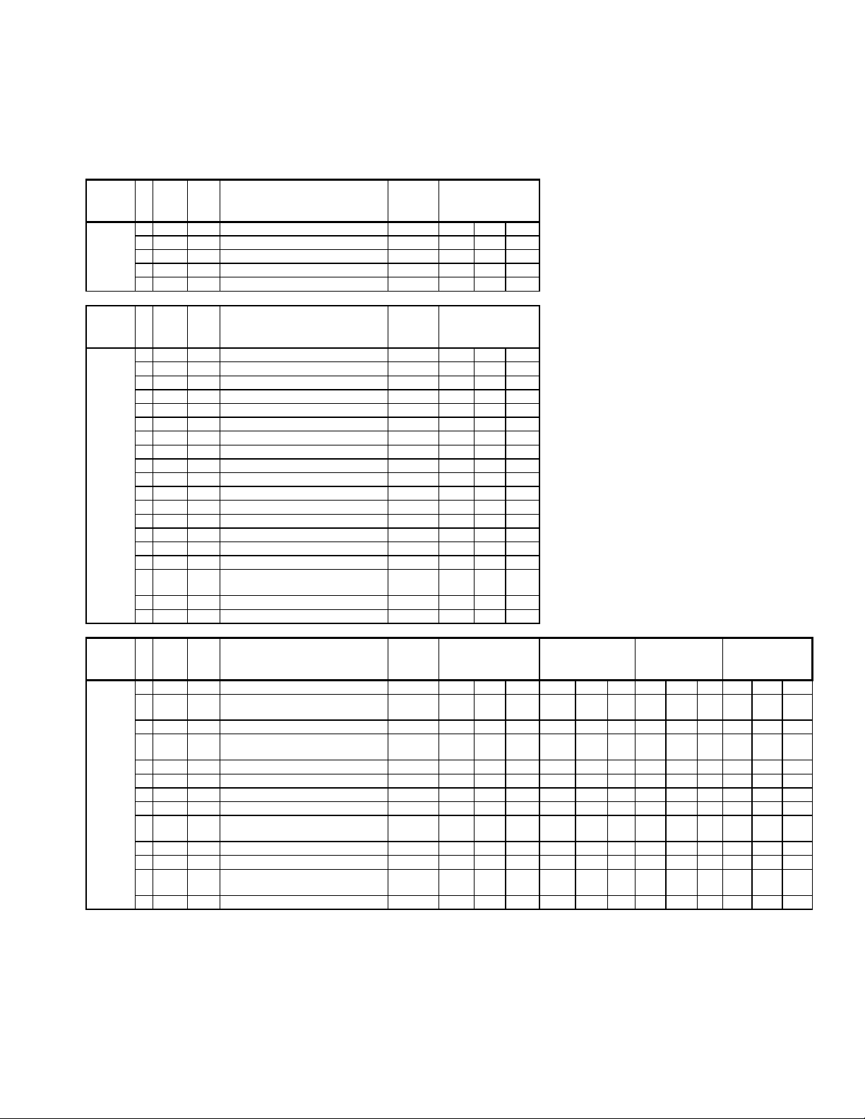
SERVICE DATA LISTS
KV-27FV300/29FV300/32FV300/36FV300
Service
3L_COMB 0 FUNN Fix Function (0 / 7-6) for NTSC 11000000 A4 3C 3
Service
3D_COMB 0 COUT Fix COUTS(00 / 2-3) 00001100 A4 21 3
Group
Group
No. Name
1 FUNP Fix Function (0 / 7-6) for PAL-N, PAL-M 00110000 A5 3C 3
2 DRNG Fix DRANG (0 / 2) 00000100 A4 3C 0
3 YCSM Fix Y/C Sep Mode (0 / 1-0) 00000011 A4 3C 0
4 CNRK Fix CNRK (1 / 7-6) 11000000 A4 3D 1
5 CNRL Fix CNR Lim (1 / 5-4) 00110000 A4 3D 1
6 CLPF Fix C-LPF(1 / 3) 00001000 A4 3D 1
7 SLPF Fix SelC-LPF(1 / 2) 00000100 A4 3D 0
8 MODE Fix Mode1 (1 / 1) 00000010 A4 3D 0
9 YPG Fix Y - Peaking Gain (2 / 7-6) 11000000 A4 3E 3
10 PDSC Fix Pds. Clip (2 / 3) 00001000 A4 3E 0
11 YLPF Fix Y-LPF(2 / 2) 00000100 A4 3E 1
12 VENL Fix V-Emph N.L (3 / 4-2) 00011100 A4 3F 4
13 VEC Fix V - Emph Core (3 / 1-0) 00000011 A4 3F 3
No. Name
1 YAPS Fix YAPS(00 / 0-1) 00000011 A4 21 1
2 NSDS Fix NSDS(01 / 4-5) 00110000 A4 22 0
3 MSS Fix MSS(01 / 2-3) 00001100 A4 22 0
4 KILS Fix KILS (01 / 1-0) 00000011 A4 22 1
5 DYC Fix DYCOS ( 02 / 7-6) 11000000 A4 23 2
6 EXAD Fix EXADINS(02 / 5) 00100000 A4 23 0
7 EXCS Fix EXCSS(02 / 1- 0) 00000011 A4 23 1
8 CPP Fix CPP(03 / 6) 01000000 A4 24 0
9 HDP Fix HDP(03 / 3-5) 00111000 A4 24 6
10 CDL Fix CDL(03 / 0-2) 00000111 A4 24 6
11 DYCO Fix DYCOR(04 / 4-7) 11110000 A4 25 2
12 DYGA Fix DYGAIN(04 / 0-3) 00001111 A4 25 10
13 DCCO Fix DCCOR(05 / 4-7) 11110000 A4 26 2
14 DCGA Fix DCGAIN(05 / 0-3) 00001111 A4 26 9
15 YNRL Fix YNRLIM(06 / 4-5) 00110000 A4 27 1
16 CNRL Fix CNRLIM(06 / 0-1) 00000011 A4 27 1
17 ID1O Fix ID1ON(07 / 7) 10000000 A4 28 0
18 ID1W Fix ID1W0A1(07 / 6) 01000000 A4 28 0
19 ID1N Fix ID1W0A2(07 / 5) 00100000 A4 28 0
20 WSC Fix WSC(08 / 6-7) 11000000 A4 29 1
21 VTRH Fix VTRH(08 / 4-5) 00110000 A4 29 1
22 VTRR Fix VTRR(08 / 2-3) 00001100 A4 29 1
23 LDSR Fix LDSR(08 / 0-1) 00000011 A4 29 2
24 WSS Fix WSS(09/7) 10000000 A4 2A 0
25 ID1E Fix ID1ECON ( 09/6) 01000000 A4 2A 1
26 TT Fix TT ( 09 / 4 -5) 00110000 A4 2A 0
27 FELC Fix FELCHK ( 09/3) 00001000 A4 2A 1
28 TH Fix TH ( 09 / 1 -2) 00000110 A4 2A 0
29 VAPG Fix VAPGAIN(0A / 5-7) 11100000 A4 2B 3
30 VAPI Fix VAPINV(0A / 0-4) 00011111 A4 2B 25
Fix /
Var
Fix /
Var
Description Bit Mask
Description Bit Mask
Common
Slave Sub Fix
Addr Addr Data
Common
Slave Sub Fix
Addr Addr Data
— 21 —

SERVICE DATA LISTS
KV-27FV300/29FV300/32FV300/36FV300
Service
3D_COMB 31 YPFT Fix YPFT(0B / 4-5) 00110000 A4 2C 3
Group
No. Name
32 YPFG Fix YPFG(0B / 0-3) 00001111 A4 2C 8
33 V1PS Fix V1PS(0C / 6-7) 11000000 A4 2D 3
34 VEGS Fix VEGS(0C / 4-5) 00110000 A4 2D 2
35 CC3N Fix CC3N(0C / 3) 00001000 A4 2D 0
36 C0HS Fix C0HS(0C / 2) 00000100 A4 2D 0
37 SEL2 Fix SELD2FH(0C / 0) 00000001 A4 2D 1
38 SEL1 Fix SELD1FL(0D / 5) 00100000 A4 2E 1
39 YHCO Fix YHCOR(10 / 6-7) 11000000 A4 31 0
40 YHCG Fix YHCGAIN(10 / 5) 00100000 A4 31 1
41 OVST Fix +OVST(10 / 3) 00001000 A4 31 0
42 CSHD Fix CSHDT(10 / 2) 00000100 A4 31 0
43 KCTT Fix KCTT(10 / 0-1) 00000011 A4 31 0
44 SHT Fix SHT(11 / 7-6 ) 11000000 A4 32 0
45 VCT Fix VCT(11/ 5) 00100000 A4 32 0
46 CGAT Fix CLKGAT ( 11 / 4) 00010000 A4 32 0
47 CG2D Fix CLK2D ( 11 / 3) 00001000 A4 32 1
48 CGGT Fix CLKGGT ( 11 / 2) 00000100 A4 32 0
49 CGEB Fix CLKGEB ( 11 / 1) 00000010 A4 32 0
50 CGT Fix CLKGT ( 11 / 0) 00000001 A4 32 0
51 HPLL Fix HPLLFS(12 / 7) 10000000 A4 33 1
52 BPLL Fix BPLLFS (12 / 6) 01000000 A4 33 0
53 FSCF Fix FSCFG(12 /5) 00100000 A4 33 0
54 PLLF Fix PLLFG(12 / 4) 00010000 A4 33 1
55 KILR Fix KILR(12 / 0-3) 00001111 A4 33 3
56 HSSL Fix HSSL(13 / 4-7) 11110000 A4 34 12
57 VSSL Fix VSSL(13 / 0-3) 00001111 A4 34 8
58 BGPS Fix BGPS(14 / 4-7) 11110000 A4 35 4
59 BGPW Fix BGPW(14 / 0-3) 00001111 A4 35 10
60 ADCL Fix ADCLKS(15 / 6-7) 11000000 A4 36 3
61 NSDW Fix NSDSW(15 / 4) 00010000 A4 36 1
62 HIZE Fix HIZEN ( 16 / 4) 00010000 A4 37 0
63 HCNT Fix HCNTFSYN ( 17 / 6) 01000000 A4 38 0
Fix /
Var
Description Bit Mask
Common
Slave Sub Fix
Addr Addr Data
— 22 —
SERVICE DATA LISTS
KV-27FV300/29FV300/32FV300/36FV300
Service
No. Name
Group
PIP 0 PFRN Fix VCXO oscilation 00000010 A4 40 0
1 PRVS Fix
2 PCON Fix PIP sub contrast control 01111111 A4 41 97
3 PUCO Fix PIP U level control 01111111 A4 42 5
4 PVCO Fix PIP V level control 01111111 A4 43 17
5 PHUE Fix PIP sub hue control 00111111 A4 57 12
6 PKIL Fix Color killer 10000000 A4 42 0
7 PSEP Fix C-sync sep input selection 11000000 A4 44 1
8 PDCN Fix Sub pic sync sep. Thereshold setting 00110000 A4 44 3
9 PBGS Fix bgp position setting 00111111 A4 45 15
10 PDL0 Fix Y/C delay adjust (for video) 00001111 A4 46 11
11 PDL1 Fix Y/C delay adjust (for yuv) 11110000 A4 46 13
12 PBRT Fix Y bryghtness control 00011111 A4 48 25
13 PVP1 Fix V pedestal level for YUV 11110000 A4 49 0
14 PUP1 Fix U pedestal level for YUV 00001111 A4 49 0
15 PVP2 Fix V pedestal level for main w/ burst 11110000 A4 4A 0
16 PUP2 Fix U pedestal level for main w/ burst 00001111 A4 4A 0
17 PVP3 Fix V pedestal level for main w/o burst 11110000 A4 4B 0
18 PUP3 Fix U pedestal level for main w/o burst 00001111 A4 4B 0
19 PACS Fix 0D, 0Eh setting mode 01000000 A4 4C 1
20 PSYS Fix Color system 00110000 = =
21 PSDL Fix Sync delay control 00000011 A4 4C 0
22 PCCL Fix YUV color level 11110000 A4 4D 11
23 PCGA Fix Croma gain 00001000 A4 4D 0
24 PAAF Fix Auto AFC 00000100 A4 4D 1
Fix /
Var
HD/VD input synchronous mode
selection
Description Bit Mask
00000001 A4 40 1
Common
Slave Sub Fix
Addr Addr Data
— 23 —
SERVICE DATA LISTS
KV-27FV300/29FV300/32FV300/36FV300
Service
No. Name
Group
PIP 25 PSU2 Fix For test 00000010 A4 4D 0
26 PCVF Fix Internal 1H comb filter 00000001 A4 4D 0
27 PBIT Fix Y clamp time constant 10000000 A4 4E 0
28 PAFC Fix AFC time constant 01000000 A4 4E 0
29 PACC Fix Color decoder amplitude 00111111 A4 4E 21
30 PSDT Fix System automatic judgment 10000000 = =
31 PBUR Fix VCXO mode selection 01000000 A4 4F 0
32 PEVE Fix Main picture PAL-N 00100000 A4 4F 0
33 PINW Fix Invert sub picture field definition 00010000 A4 4F 0
34 PINR Fix Invert main picture field definition 00001000 A4 4F 0
35 PVMD Fix Vertical display mode when pal-n 00000100 = =
36 PREF Fix Main picture field fix 00000010 A4 4F 0
37 PARE Fix Automatic 50/60 Hz judgement 00000001 A4 4F 0
38 PBWD Fix BW det. Treshold setting 00110000 A4 50 1
39 PFRA Fix Freq. Adjustment for free run mode 00001111 A4 51 0
40 PPAL Fix Parameter setting for PAL-M judgment 11111111 A4 52 52
41 PHPO Fix Sub picture h position 00111111 A4 58 3
42 PVPO Fix Sub picture v position 00111111 A4 59 22
43 PHTI Fix Display timing adjust 00001111 A4 44 3
44 PHAJ Fix Main/Sub switch delay control 11110000 A4 47 2
45 PBGY Fix Back ground Y level setting 00001111 A4 53 0
46 PCRO Fix Sub picture read mode 10000000 A4 54 0
47 PPAR Fix
48 PHPF Fix Y output HPF 00010000 A4 51 0
49 PFSC Fix FSC output 10000000 A4 43 0
50 PVCH Fix 15h,16h,17h, setting mode 00000100 A4 4C 0
51 PVON Fix V-chip decode mode 10000000 A4 53 1
52 PVLN Fix V-chip data slicer line selection 00011111 A4 54 17
53 PVSB Fix
54 PVLV Fix V-chip data slicer slice parameter 11111111 A4 56 130
55 SUSW Fix Sub-Unlock bit position switch 01000000 A4 59 0
Fix /
Var
Thereshold contol for ident judgement of
sub
V-chip data slicer start bit detection
parameter
Description Bit Mask
00001111 A4 50 1
11111111 A4 55 64
Common
Slave Sub Fix
Addr Addr Data
— 24 —
SERVICE DATA LISTS
KV-27FV300/29FV300/32FV300/36FV300
Service
Service
Service
No. Name
Group
AP 0 SBAL Fix Sub Balance 00000111 A8 41 4 A8 41 4
1 SBAS Fix Sub Bass 00000111 A8 43 4 A8 43 4
2 STRE Fix Sub Treble 00000111 A8 42 0 A8 42 0
3 SRL Fix Surround level 00000001 A8 44 0 A8 44 0
4 BBOH Fix Surround Off - BBE high 11110000 A8 45 10 A8 45 10
5 BBOL Fix Surround Off - BBE low 00001111 A8 45 5 A8 45 5
6 BBSH Fix Simulated - BBE high 11110000 A8 46 0 A8 46 0
7 BBSL Fix Simulated - BBE low 00001111 A8 46 0 A8 46 0
8 BBMH Fix Surround - BBE high 11110000 A8 47 0 A8 47 0
9 BBML Fix Surround - BBE low 00001111 A8 47 0 A8 47 0
10 BBGH Fix WOW - BBE high 11110000 A8 48 6 A8 48 6
11 BBGL Fix WOW - BBE low 00001111 A8 48 9 A8 48 9
12 BBTH Fix Trusurround - BBE high 11110000 A8 49 7 A8 49 7
13 BBTL Fix Trusurround - BBE low 00001111 A8 49 8 A8 49 8
14 VFIX Fix Audio output fix data 11111111 A8 4A 244 A8 4A 244
15 AGCL Fix AGC Level 00000110 A8 44 2 A8 44 2
No. Name
Group
CCD 0 DUM0 Fix Only for testing 11111111 = =
1 VOSD Fix Only for testing 00000001 = =
No. Name
Group
OP 0 DISP Fix OSD Display position 00111111 A4 06 28
1 RAMW Fix 00000001 = =
2 ICMP Fix
3 IPOR Fix 0:Even, 1: Odd, Other: do not change 00000011 A4 3A 1
4 FAWD Fix 1: Forced to auto wide mode, 0:normal 00000100 A0 5D 0
5 HCLW Fix H-Count Lower limit 11111111 A4 02 67
6 HCHG Fix H-Count Higher limit 11111111 A4 03 254
7 9VTM Fix Delay for 9V check subsystem 11111111 A4 04 55
8 ZDET Fix Zero detect relay delay 11111111 A4 05 123
Fix /
Var
Fix /
Var
Fix /
Var
Comparison data to determine Noninterlace signal for OSD
Description Bit Mask
Description Bit Mask
Description Bit Mask
00011111 A4 39 4
KV-27FV300/29FV300 KV-32FV300/36FV300
Slave Sub Fix Var Slave Sub Fix Var
Addr Addr Data Data Addr Addr Data Data
Common
Slave Sub Fix
Addr Addr Data
Common
Slave Sub Fix
Addr Addr Data
Service
No. Name
Group
ID 0 ID0 Fix Model variation ID0 11111111 A4 78
1 ID1 Fix Model variation ID1 11111111 A4 79
2 ID2 Fix Model variation ID2 11111111 A4 7A
3 ID3 Fix Model variation ID3 11111111 A4 7B
4 ID4 Fix Model variation ID4 11111111 A4 7C
5 ID5 Fix Model variation ID5 11111111 A4 7D
6 ID6 Fix Model variation ID6 11111111 A4 7E
7 ID7 Fix Model variation ID7 11111111 A4 7F
Fix /
Var
To determine ID's value, ID map must be refered
Description Bit Mask Var Data
Slave
Addr
— 25 —
Sub
Addr
SEE ID MAP
SEE ID MAP
SEE ID MAP
SEE ID MAP
SEE ID MAP
SEE ID MAP
SEE ID MAP
SEE ID MAP
KV-27FV300/29FV300/32FV300/36FV300
4-5. ID MAP TABLE
Model Destination ID-O ID-1 ID-2 ID-3 ID-4 ID-5 ID-6 ID-7
KV-27FV300 US 89 63 237 98 78 128 6 16
KV-27FV300 CND 89 63 237 82 78 128 6 16
KV-29FV300 E 81 63 237 194 110 128 6 80
KV-32FV300 US 89 63 237 98 78 128 6 24
KV-32FV300 CND 89 63 237 82 78 128 6 24
KV-36FV300 US/HAW 89 63 237 98 78 128 6 24
KV-36FV300 CND 89 63 237 82 78 128 6 24
4-6. A BOARD ADJUSTMENTS
H. FREQUENCY (FREE RUN) CHECK
1. Input a TV mode (RF) with no signal.
2. Connect a frequency counter to base of Q501
(TP-25 H. DRIVE) on the A Board.
3. Check H. Frequency for 15734 ± 400/-200 Hz.
V. FREQUENCY (FREE RUN) CHECK
1. Select video 1 with no signal input.
2. Set the conditions for a standard setting.
3. Connect the frequency counter to TP-27 (V OUT) or CN501 pin
6
(V DY+) and ground on the A Board .
4. Check that V. Frequency shows 60 ± 5 Hz.
SUBCONTRAST ADJUSTMENT (RDRV)
1. Input a color-bar signal and set the level to 75%.
2. Set in Standard mode.
3. Activate the Service Adjustment Mode. Set color min pic max.
4. Set GON and BON items. Using
values. Leave RON set to “1”.
3
and 6 set each to the following
7. Adjust the value of SCON with
3
and 6 for
1.90 ± 0.05Vpp for 27/29/32/34”, or 1.95 ± 0.05Vpp for 36/38”.
8. Reset AALS, ABLS, GON and BON values to “1”.
R ON: ON (1)
G ON: ON (1)
B ON: ON (1)
9. Press
MUTING
then
ENTER
to save into the memory.
DISPLAY POSITION ADJUSTMENT (DISP)
1. Input a color-bar signal.
2. Set to Service Adjustment Mode.
3. Select DISP with
4. Adjust values of DISP with
center.
5. Write to memory by pressing
6. Check to see if the text is displayed on the screen.
Signal
Type
1
and 4 .
3
and 6 to adjust characters to the
MUTING
Mode
Category
service micro disp 48
ntsc
vchp
Display
Item
00000000 00000000
then
Item
Data
ENTER
.
Mode
service video rdrv
Signal
Type
ntsc
vchp
Category
Display
00000000 00000000
Item
26
Item
Data
R ON: ON (1)
G ON: OFF (0)
B ON: OFF (0)
5. Connect an oscilloscope probe to C Board, CN705 pin 3 (Red Out)
(TP35).
6. Select SCON with
1
and 4 .
— 26 —
SUB BRIGHT ADJUSTMENT (SBRT)
1. Input a monoscope signal.
2. Activate the Service Adjustment Mode.
3. Set the PICTURE and BRIGHTNESS to minimum.
4. Select the SBRT item with
5. Adjust the values of SBRT with
1
and 4 .
3
and 6 to obtain a faintly visible
crosshatch.
6. Press
MUTING
then
ENTER
to save into the memory.
SUB HUE, SUB COLOR ADJUSTMENT
(SHUE, SCOL)
1. Input color-bar signal at 75%.
2. Activate the Service Adjustment Mode.
3. Set (PIC) to Max and (COL) to 50%.
4. Connect an oscilloscope probe to C Board, CN705Pin
1
5. Select the SHUE and SCOL item with
and 4 .
4
Blue Out.
KV-27FV300/29FV300/32FV300/36FV300
1
6. While showing the SHUE item, adjust the waveform with
4
and
until the second and third bars show the same level
(V2 = V3 < 0.15Vp-p).
7. While showing the SCOL item, adjust the waveform with
6
and
until the fi rst and fourth bars show the same level
(V1 = V4 < 0.15Vp-p).
8. Press
MUTING
then
V2 V3
V1
ENTER
V4
to save into the memory.
3
V. SIZE ADJUSTMENT (VSIZ)
1. Input a crosshatch signal.
2. Activate the Service Adjustment Mode.
3. Select the VSIZ item with
4. Adjust value of VPOS with
5. Press
MUTING
then
1
and 4 .
1
and 4 for the best vertical center.
ENTER
to save into the memory.
H. SIZE ADJUSTMENT (HSIZ)
1. Input a monoscope signal.
2. Activate the Service Adjustment Mode.
3. Select HSIZ with
4. Adjust with
5. Press
MUTING
1
and 4 .
3
and 6 for the best horizontal size.
ENTER
then
to save into the memory.
V. LINEARITY (VLIN), V. CORRECTION
(SCOR), PIN AMP (PAMP), AND HORIZONTAL
TRAPEZOID (HTRP) ADJUSTMENTS
1. Input a crosshatch signal.
2. Activate the Service Adjustment Mode.
3. Select VLIN, SCOR, PAMP, and HTRP with with
4. Adjust with
5. Press
3
and 6 for the best horizontal size.
MUTING
then
V LINEARITY (VLIN)
ENTER
to save into the memory.
1
and 4.
V. CENTER ADJUSTMENT (VPOS)
Perform this adjustment after performing H. Frequency
(Free Run) Check.
1. Input a crosshatch signal.
2. Activate the Service Adjustment Mode.
3. Select the VPOS item with
4. Adjust value of VPOS with
5. Press
MUTING
then
1
and 4 .
3
and 6 for the best vertical center.
ENTER
to save into the memory.
H. CENTER ADJUSTMENT (HPOS)
Perform this adjustment after performing H. Frequency
(Free Run) Check.
1. Input a crosshatch signal.
2. Activate the Service Adjustment Mode.
3. Select the HPOS item with
4. Adjust the value of HPOS with
5. Press
MUTING
then
1
ENTER
and 4 .
3
and 6 for the best horizontal center.
to save into the memory.
V CORRECTION (SCOR)
PIN AMP (PAMP)
HORIZONTAL TRAPEZOID (HTRP)
— 27 —
V. ANGLE (VANG), V. BOW (VBOW), UPPER
PIN (UPIN) AND LOW PIN (LPIN)
ADJUSTMENTS
1. Input a crosshatch signal.
2. Activate the Service Adjustment Mode.
3. Select VANG, VBOW, UPIN, and LPIN with
4. Adjust with
5. Press
3
and 6 for the best picture.
ENTER
MUTING
then
V ANGLE (VANG)
V BOW (VBOW)
to save into the memory.
1
and 4.
KV-27FV300/29FV300/32FV300/36FV300
UPPER PIN (UPIN)
LOW PIN (LPIN)
SERVICE ADJUSTMENT MODE MEMORY
ENTER
0
Item
then
Item
Data
7
.
Green
0
Red
ENTER
1. After completing all adjustments, press
Read From Memory
Mode
service defl vbow
Signal
Type
ntsc
vchp
Category
Display
00000000 00000000
— 28 —
5-1. CIRCUIT BOARDS LOCATION
KV-27FV300/29FV300/32FV300/36FV300
SECTION 5: DIAGRAMS
The components identifi ed by shading and ! symbol are critical for safety. Replace
only with part number specifi ed.
The symbol indicates a fast operating fuse and is displayed on the component
side of the board. Replace only with fuse of the same rating as marked.
C Board
V Board
HR Board
GK Board
A Board
T Board
5-2. PRINTED WIRING BOARDS AND
SCHEMATIC DIAGRAMS INFORMATION
All capacitors are in µF unless otherwise noted. pF : µµF 50WV or less
are not indicated except for electrolytics and tantalums.
All electrolytics are in 50V unless otherwise specifi ed.
All resistors are in ohms. kΩ=1000Ω, MΩ=1000kΩ
Indication of resistance, which does not have one for rating
electrical power, is as follows: Pitch : 5mm
Rating electrical power :
1
/
W in resistance, 1/
4
W and 1/
10
W in chip resistance.
8
: nonfl ammable resistor
: fusible resistor
: internal component
: panel designation and adjustment for repair
: earth ground
: earth-chassis
All variable and adjustable resistors have characteristic curve B, unless
otherwise noted.
Readings are taken with a color-bar signal input.
Readings are taken with a 10MΩ digital multimeter.
Voltages are DC with respect to ground unless otherwise noted.
Voltage variations may be noted due to normal production tolerances.
All voltages are in V.
S : Measurement impossibility.
: B+line
: B-line (Actual measured value may be different).
: signal path (RF)
Circled numbers are waveform references.
1
/
W
4
Les composants identifi es per un trame et une marque
securite. Ne les remplacer que par une piece portant le numero specifi e.
Le symbole indique une fusible a action rapide. Doit etre remplace par une
fusible de meme yaleur, comme maque.
!
sont critiques pour la
The components identifi ed by X in this basic schematic diagram have
been carefully factory-selected for each set in order to satisfy regulations
regarding X-ray radiation. Should replacement be necessary, replace
only with the value originally used.
When replacing components identifi ed by
Y
, make the necessary
adjustments as indicated. If the results do not meet the specifi ed value,
change the component identifi ed by
X
and repeat the adjustment until
the specifi ed value is achieved.
(Refer to R530 and R531 adjustment on page 16.)
When replacing the parts listed in the table below, it is important to
perform the related adjustments.
Part Replaced () Adjustment ()
A BOARD: HV HOLD DOWN
R550, T503, T504, D519,
R530, R531
IC501, R533, D521, R532,
D520, C531, R529, R530,
R531, C532
REFERENCE INFORMATION
RESISTOR
: RN METAL FILM
: RC SOLID
: FPRD NONFLAMMABLE CARBON
: FUSE NONFLAMMABLE FUSIBLE
: RW NONFLAMMABLE WIREWOUND
: RS NONFLAMMABLE METAL OXIDE
: RB NONFLAMMABLE CEMENT
: ADJUSTMENT RESISTOR
COIL
: LF-8L MICRO INDUCTOR
CAPACITOR
: TA TANTALUM
: PS STYROL
: PP POLYPROPYLENE
: PT MYLAR
: MPS METALIZED POLYESTER
: MPP METALIZED POLYPROPYLENE
: ALB BIPOLAR
: ALT HIGH TEMPERATURE
: ALR HIGH RIPPLE
— 29 —
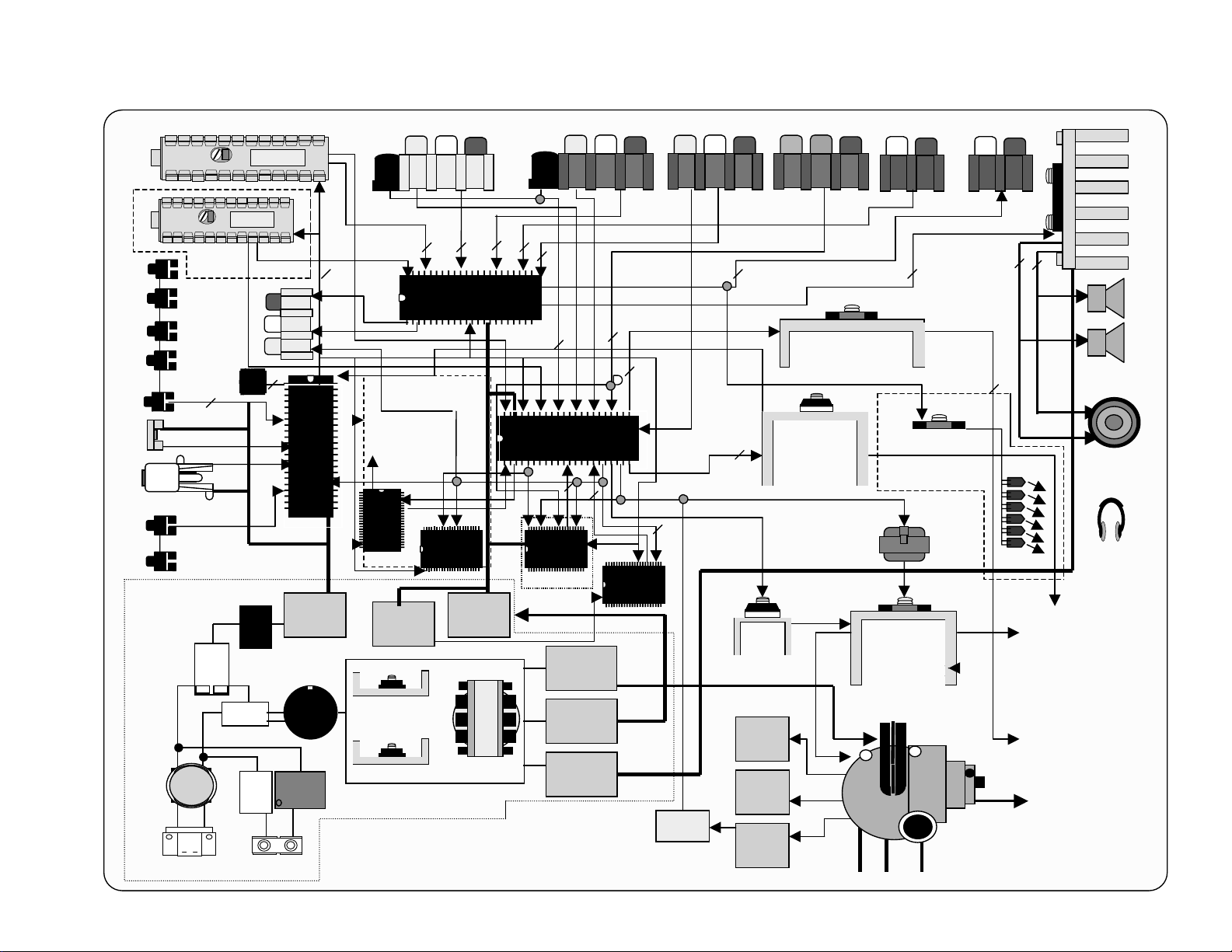
5-3. BLOCK DIAGRAM AND SCHEMATICS
KV-27FV300/29FV300/32FV300/36FV300
Tuner FRONT
Tuner
P board
Sub det-Out
2
L
MOUT
2
2
R
L
V
Mircoprocessor
M306V5ME
I.R.
Det. out
S
REAR
V1 LR
2
2
Audio Processor
NJW1134
I2C Bus
Iprot
(For FV only)
BC board
Y/C
2
2
2
Video processor
CXA2154/5AS
YUV
SRT
TA1226N
5V
Reg.
Yout
Yin
3D comb
MN82832.
9V
Reg.
C
PinP Proc.
M65665FP.
P board
SRT
L.E.D.
Energy Star
G board
Menu
CTRL
5VDC
TV-8
DEC
5V
STBY
S
V2 LR
4
3
B+
Rect.
3
3 RGB
TV-8
2
Y/C
3L comb
TC90A69.
For FS only
135V
REAR
V3 LR
CVBS,FSC
2
2
Vd
V-Out
AN5522 (24-27”)
2
STV9379(32-36”)
Hp
E/W
Pin
Out
2SC4159
YUV AUDIOYUV
Y UV
RGB Driver
TDA6108
LR
Audio Amplifier
TDA8580J
10W&15W
2
IR modulator
BA3308
T board
H.Drive
H-Out
2SD2634(27”)
2SD2645(32-36”)
AUDIO OUT
LR
2
2
3RGB
Emiter
Vert.
Horiz.
To DY
R
L
Speakers
Sub woofer
(for FV only)
IR Head
phones
L.F.T
AC Line
Rect.
Relay
THP
D.G.C.
Power Mosfet
2SK2876
Power Supply
Low B
Rect.
Audio
Rect.
12.5V
24V
— 30 —
OCP
200v
Rect.
+13v
Rect.
-13v
Rect.
G2
FBT
HV
Focus
To CRT
To CRT
FBT
27”-NX4521
32-36”-NX4600

A BOARD SCHEMATIC DIAGRAM
1 | 2 | 3 | 4 | 5 | 6 | 7 | 8 | 9 | 10 | 11 | 12 | 13 | 14 | 15 | 16 | 17 | 18 | 19 | 20 | 21 | 22 | 23 |
A
V
V
—
B
—
C
STEREO
0
9
3
CN600
C050
470
25V 47
L004
9V
9V
TP602
D009
MTZJ-T-77-30
—
TMR
D
TO HR BOARD
CN3001
CN003
LED
MAIN PWR LED
5V STBY
6P
1
2
GND
3
4
SIRCS
5
POWER
6
—
E
—
F
—
G
—
TO HU BOARD
CN1001
TO HU BOARD
CN1003
TO HU BOARD
CN1002
CN004
CN005
CN006
5P
CN001
MENU
VIDEO-2
FRONT-L
FRONT-R
C2/MENU
B-CLK
B-DAT
B-INT
1
KEY
2
GND
3
Y2
1
2
GND
GND
3
4
1
GND
2
3
4
GND
5
4
3
2
1
GND
Q402
2SD601A
MUTE
Q403
2SD601A
MUTE
J207
VAR/FIXED
2P
R405
2.2k
R416
4.7k
3P
4P
4P
FOR
JIGS
H
J204
3P
MNTR OUT
—
I
J205
AUDIO IN
2P
—
J206
3P
J
—
YPBPR
J203
REAR VIDEO
3P
K
SW
—
J201
S VIDEO
4P
1342
L
CN502
10P
—
M
—
N
—
TO V BOARD
TO C BOARD
CN901
DF-HDRV
H-TRAP
NS-MUTE
CN705
CN303
8P
B+
1
NC
2
GND
3
GND
4
9V
5
9V
6
VM
7
8
HP
VD+
9
10
8
7
6
N/S
G
5
B
4
R
3
GND
2
I-K
1
O
—
P
KV-27FV300/29FV300/32FV300/36FV300
C453
0.1
R209
R207
100k
:CHIP
0.001
:CHIP
C060
220p
0
_
Y
S
2
0.001
C033
1
6.3V
CHIP
K
L
C
R058
100k
:CHIP
100k
:CHIP
MTZJ-T-77-9
MTZJ-T-77-9
C417
25V
NJM2188M-TE2
AUDIO FILTER
MTZJ-T-77-6.2B
R010
220
C018
220p
CHIP
C120 C121
CHIP
O
I
R
H
P
I
_
-
M
Z
U
E
T
R
E
O
C034
CHIP
R035
220
:CHIP
5678
T
A
D
:CHIP
R
D201
D200
C202
0.1
16V
D111
L010
10p
C035
0.001
R056
220
R057
100k
C203
0.1
16V
R951 R406
R210
220
IC402
L001
D010
MTZJ-T-77-5.6C
C017
0.0022
R120
470
C016
10p
470
CHIP
25V
I
0
_
_
V
0
O
C
S
S
C
C
C
O
O
-
-
S
3
U
D
B
R
I
T
E
-
M
S
O
U
E
C
T
T
P
1
0
3
2
1
C036
2
R
0.001
R060
CHIP
220
R064
220
R132
4.7k
A
D
S
R391
75
A
V
C
11
I
O
S
D
A
T
I
_
9
V
C
H
E
C
K
100
10k
H
T
C
IC400
3
1
1
D
R401
100
:CHIP
C004
47 25V
C
1
.
5
7
7
T
J
Z
T
M
F:CHIP
F:CHIP
L
T
C
B
V
C
:CHIP
R016
I
A
F
T
S
U
B
:CHIP
R052
100k
220
I
O
B
D
A
T
R032
220
R054
C367
0.47
10V
C368
0.47
10V
1k
R6002
MTZJ-77-9.1B
F
S
E
B
R
C
V
L
A
C
D
S
S
:CHIP
AUDIO R
R051
1M
:CHIP
R015
220
I
O
B
C
L
K
N
I
A
F
T
R033
:CHIP
R6003
10k
:CHIP
10k
:CHIP
D307
R394
75
:CHIP
C420C418C416C414C412
14.7112.2
C422
470
2122232425262728293031323334353637383940
+
V
D
N
G
R403
100
C031
220p
:CHIP
C030
0.047
C122
0.1
16V
16V
R113
100
R013
C003
10k
0.1
:CHIP
16V
:CHIP
I
0
I
O
S
C
L
K
N
I
M
E
N
U
_
N
V
M
_
W
P
I
K
E
Y
R139
C028
0.001
CHIP
R038
C045
10
:CI
220
1k
ZERO DET
_
I
R
H
P
2
I
H
S
Y
N
C
S
U
B
R034
220
:CHIP
V
5
Y
B
T
S
1 2 3 4
BR24C16F-E2
MEMORY
Q6000
2SD601A
B
4
0
1
R
IC003
O
_
Y
M
I
H
S
Y
N
C
_
M
A
I
N
0
2
2
P
W
G
D306
R390
75
AUDIO L
AUDIO R
C206
0.1
16V
R217
100k
:CHIP
R218
100k
:CHIP
MTZJ-T-77-9
9
3
0
R
0
k
3
7
1
.
R
4
9
0
2
2
1
2
R
3
R030
0
1
47k
R
:CHIP
:CHIP
C207
0.1 16V
D210
9V
B
B
1
2
N
N
I
I
A
A
2
1
N
N
I
I
1 2 3 4 5 6 7 8 9
k
7
.
4
k
7
.
4
BD4743G-TR
C101
0.001
25V
:CHIP
C365
100p
500V
2
T
R098
1k
AGC
Q407
2SD601A
T
D
U
U
O
N
D
O
O
N
T
C
N
D
3
1
2
M
T
Z
J
T
7
7
9
.
1
B
E
T
U
C
M
N
C201 C200
0.1
16V
B
*
8
2
1
R
U
O
R
R202
220
:CHIP
R206
220
:CHIP
Q404
BUFFER
T
U
O
L
0.1
16V
B
*
V
9
I
N
E
O
I
T
T
D
M
P
E
E
O
A
T
D
D
M
F
S
S
V
I
D
E
O
R099
100
:CHIP
R126
*
R124
*
9
-
7
2
1
2
D
7
-
T
-
J
Z
T
M
3
0
4
C
I
MA111-TX
R224
H
C
T
I
W
S
L
*
D412
B
1
.
9
3
-
1
220
7
3
7
D
T
J
Z
T
M
B
0
1
-
5
7
0
7
0
-
D
T
J
Z
T
M
Q406 IC002
*
BUFFER
SW
C6002
47
25V
T
V
9
R086
33k
:CHIP
MTZJ-T-77-5.1C
R222
100k
:CHIP
D219
3
V
N
I
P
I
P
N
I
N
I
A
M
N
I
D
R
G
N
I
D413
C6001
330
25V
TU001
U
O
BTF-WA421
T
D
F
N
A
G
Q002
2SD601A
BUFFER
R087
22k
:CHIP
R089
Q005
4.7k
2SD601A
DET OUT
TP102
D004
Q405
*
BUFFER
R223
220 :CHIP
C208
0.1
C209
16V
0.1
16V
R225
100k
:CHIP
D211
MTZJ-T-77-9
R037
4.7k
220
:CHIP
R234
220 :CHIP
9
10111213141516
1
3
2
P
P
P
H
H
H
R
R
R
I
I
I
D
H
D
N
N
N
G
I
G
9
10111213141516
1
3
2
3
P
V
P
P
H
N
H
H
-
I
-
-
R
R
R
I
I
I
P
I
P
-
D
H
D
N
N
N
N
I
G
J
G
C443
*
R412
1k
IO
G
C102
0.001
25V
:CHIP
C
G
L
A
V
C
D
S
5
S
S
A
8
0
0
0
1
1
R
C049
10
R107
100
:CHIP
C055
100
16V
L009
TP603
5V
R408
2.2k
V
L
A
F
F
I
R
V
TP100
RF-AGC
6.3V
C051
C052
25V
0.0047
L003
C054
4.7
R085
15k
3W
5
7
4
4
1
R
R232 R235
C212
MTZJ-T-77-9
4.7
470k
:CHIP
C213
4.7
R233
470k
D218
MTZJ-T-77-9
D
1
N
2
D
V
I
V
V
S
A
S
N
M
N
I
N
I
I
IC404
* R SWITCH
P
D
D
A
H
N
N
V
T
G
G
N
U
N
N
I
O
I
I
1 2 3 4 5 6 7 8
C442
*
1
2
D
V
V
D
S
S
V
N
N
I
I
D
P
R
4
H
G
V
-
-
-
T
N
N
U
I
I
O
1 2 3 4 5 6 7 8
R
R402 R404
**
MTZJ-T-77-7.5B
R411
470
R413
10k
IC6008
NJM2930F05
5V REG
MTZJ-77-9.1B
C366
R219
0.47
220
10V
:CHIP
F:CHIP
D209
MTZJ-T-77-9
R220
220 :CHIP
C400
0.33
10V
R400
4.7k
0.00330.0082
25V
B
B
B
B
B
B
2
N
1
5
3
4
6
L
O
E
N
N
N
N
I
M
B
I
I
I
I
F
B
S
R
S
S
A
S
A
A
A
A
A
4
3
N
N
I
I
1
/
N
6
5
E
S
O
N
N
B
R
M
I
I
B
S
C401
0.022
25V
C403
0.0033
H SYNCH SEP
R123
*
R125
*
4.7k
R019
4.7k
R023
P
6
2
/
R
X
D
0
0
_
I
R
H
P
7
k
0
0
0
1
R
1
NC
2
GND
3
GND
RESET
D006
MTZJ-10B
3
V
5
33 34 35 36 37 38 39 40 41 42 43 44 45 46 47 48 49 50 51 52 53 54 55 56 57 58 59 60 61 62 63 64
C026
220p
CHIP 220
R127
*
R137
R136
4.7k
4.7k
R071
47k
R102
4.7k
:CHIP
R101
4.7k
:CHIP
R078
47k
:CHIP
VCC
5
C048
0.001
4
RESET
YUY SW
CHIP
C046
10
C047
470
25V
D305
MTZJ-77-9-1B
R393
75
:CHIP
C408
0.0015
AUDIO L
C406C404C402
0.033
16V
C410
0.22
16V
B
B
B
L
S
B
B
H
2
-
R
E
-
-
E
E
C
N
T
E
B
N
I
U
N
B
O
O
T
L
O
T
NJW1134G-TE2
A
AUDIO PROCESSOR
A
A
H
A
L
-
-
A
E
-
E
E
N
N
O
O
T
T
C409
0.22
16V
10
R018
220
4.7k
O
B
O
M
O
N
O
R025
:CHIP
R027
220
:CHIP
T
N
U
I
O
L
C411
0.33
10V
R053
1k :CHIP
220
O
O
-
-
G
R
O
I
-
-
S
S
A
A
P
P
C027
0.001
B:CHIP 1k
R029
220
C
1
.
5
2
-
0
7
0
7
D
T
J
Z
T
M
C6003
1
6.3V
:CHIP
R6004
1k
:CHIP
C
G
A
C413 C415
R061
47k
R031
R6001
2
E
B
B
10 11 12 13 14 15 16 17 18 19 20
C405
0.033
16V
C407
0.0015
C032
Q001
2SB709A
L002
1 6.3V
C062
R017
R021
P
6
3
/
T
X
D
0
0
_
T
R
V
_
S
U
R
R
R055
47k
25V
Q315 Q400
R208
2SB709A
220
BUFFER
:CHIP
C397
220 2.2k
R950
100
C426
10
CHIP
I
_
X
I
N
O
T
M
U
T
E
C037
220p
CHIP
R066
10k
R065
47k
R395
100
16V
75
R396
470k
D308
MTZJ-77-9.1B
N
I
H
C
L
1
E
D
O
M
1 2 3 4 5 6 7 8
R420
1.8k
C434
0.0047
X001C015
10MHz22p
G
N
D
O
M306V5ME-109SP UPROCESSOR
A
G
C
M
U
T
E
R133
47k
R134
220
C6005
2200
16V
MTZJ-T-77-9.1B
AUDIO L
C428
0.01
25V
16V
C427
10
N
2
1
3
T
I
N
N
N
U
I
I
I
O
H
C
1
1
1
1
R
L
L
L
L
I
I
I
I
T
F
F
F
F
N
U
I
O
2
2
F
2
E
L
E
L
D
I
R
I
+
O
F
V
F
V
M
R421
120k
C432
100
25V
R425
56k
R426 C435
1.5k 0.0047
C433
0.01
25V
R050
10k
:CHIP
R004
R009
1M
0
CHIP
C014
22p
CHIP
1011121314151617181920212223242526272829303132
I
0
C
-
_
N
R
X
V
E
O
S
S
U
S
E
T
T
IC001
O
I
-
-
I
M
P
-
M
O
B
U
W
I
T
E
N
E
R
T
N
C133
C038
220p
220p
CHIP
R409
150
R070
220
C043
220p
5
CHIP
0
3
2
D415
1
2
R
1SS133
10k
:CHIP
9
k
5
0
3
1
R
R228
100k
C210
4.7
C211
D217
10111213141516
R006
I
S
I
R
C
S
0
_
A
M
U
T
E
C039
0.001
:CHIP
4.7
MTZJ-T-77-9.1B
R231
220
C430C429 R355
0.00470.22
AUDIO R
C431
0.22
16V
9
T
T
U
U
O
O
H
H
C
C
L
R
2
N
I
2
2
M
L
D
2
2
I
N
4
.
F
G
R
2
3
k
2
3
4
3
R
R424
68k
C029
1
R140
220
R005
1k
C009
C007
:CHIP
0.0011k220p
CHIP
C008
1
0
I
-
O
-
I
-
R
H
N
H
L
S
P
F
1
0
-
O
O
A
-
-
N
Y
A
U
T
N
V
S
T
W
-
S
_
S
W
0
W
1
X
T
1
1
1
A
C111
M
220p
0
1
4
D
C041
220p
CHIP
R114
220
R076
47k
:CHIP
Q590
2SD601A
HP PROT
R590
100
R591
1k
D590
1SS133T-77
TP89
E/W DRIVE
B
+
R533
47k
1W
:RS
1SS133T-77
2SD601A
BUFFER
R229
100k
R230
220
D213
MTZJ-77-9.1B
R303
560
:CHIP
1
R302
470
:CHIP
Q300
2SB709A
BUFFER
C300
R300
0.47
25V
R048
4.7k
R003
470
:CHIP
C006
0.001
CHIP
C005
560p
CHIP
I
I
-
A
V
C
V
V
H
V
S
C
O
I
S
C
L
N
D
0
0
_
_
T
M
I
_
P
W
R
L
E
D
2SD601A
C020
220p
:CHIP
D007
MA111-TX
D508
O
M
-
E
R
R
O
E
_
-
L
L
D
A
E
G
Y
D
C
R075
220
R073
4.7k
Q004
SW
R011
1k
:CHIP
D008
MA111-TX
R012R068
3.3k
:CHIP
C502
0.47
R501 C554
* *
Q501
2SC3209LK-TP
H DRIVE
C503
470p
:CHIP
R502
4.7k
R540
1M
:CHIP
R581
220k
R515
18k
:CHIP
C521
0.001
B:CHIP
R516
*
C534
47
D522
1SS133T-77
1SS133
9V
Q401
2SD601A
BUFFER
R407
2.2k
JW(10.0MM)
D303
R354
4.7k
Q314
2SD601A
BUFFER
R002
R353
220
6.8k
:CHIP
R301
100
:CHIP
3
.
R385
3
O
-
220
2
7
E
0
7
3
D
-
D
T
I
-
V
J
Z
T
M
0
R001
10k
:CHIP
C002
220p
B
:CHIP
2
.
6
2
-
1
7
1
7
D
T
J
C001
Z
T
470p
M
CHIP
123456789
I
I
-
-
H
V
P
P
U
U
L
L
S
S
E
E
0
_
M
0
O
_
N
H
_
T
S
R
W
P
R077
100
C044
k
1
220p
CHIP
4
7
0
R
R384
39k
:CHIP
R552
JW(7.5MM)
R539
JW(7.5MM)
C506
0.047
200V
R503
4.7k
C504
17 18
470p
500V
+12V
R545
3.3
:FPRD
JW501
5MM
R517
1k
R518
2SC2412K-T-146-Q
10k
:CHIP
C528
0.0022
:CHIP
+
C
C
V
1 2 3 4
JR002
0
:CHIP
C532
D520
D521
MTZJ-7.5X
R117
22k
K
I
R022 R024
680
1/16W
:CHIP
K
I
R020
680
1/16W
:CHIP
R504
*
1
3
C505
470p
500V
C522
1
R519
470
Q511
PIN-DRIVE
D536
MA111TX
1SS133 CLAMP
5678
NJM2903M-TE2
PIN-CONTROL
C
C
V
R529
56k
22
R532
120
:CHIP
C364
47p
:CHIP
2SD601A
BUFFER
R386
100k
:CHIP
3
8
3
R
1/16W
:CHIP
T501
:HDT
R506
47
1W
:RS
C520
2200p
500V
C519
100p
500V
D516
C530
0.0022
:PT
IC501
C571
1000 25V
22k :CHIP
R530R531
12k
:CHIP
R343
R387
0
:CHIP
Q306
R344
470k
:CHIP
R345 R346
100k
:CHIP
k
2
.
2
680
G
D501
MTZJ-5.6C
4
5
6
R513
JW(12.5MM)
2SD2645-YB
D535
MA111TX
:CHIP
Q110
2SB709A
SW
R912
1k
:CHIP
10k
100k
:CHIP
19
Q502
H OUT
R526
L511
8mH
RGP1004GT
PIN-OUT
2SC4159-E
PIN OUT
R528
22k
H.PRT
C531
22
R118
22k
2SD601A
R
D507
R507
47
*
FB503
1.1UH
D515
C525
220p
500V
Q512
R523
R525
8.2k
TP85
Q319 Q317
BUFFER
C327
0.1
16V
B:CHIP
R342
33k
CHIP
R347
2.2k
:CHIP
R352
0
Q307
2SB709A
BUFFER
1k :CHIP
10k :CHIP
C325
47p
:CHIP
R341
*
2SB709A
BUFFER
C330
R909
R910
2SD601A
H
P
/
P
R
O
T
E
C
T
33 34 35 36 37 38 39 40 41 42 43 44 45 46 47 48 49 50 51 52 53 54 55 56 57 58 59 60 61 62 63 64
R381
C359
330p
B
1SS133T-77
R505
2kV
B
FB501
1.1UH
PIN
1.8 1/2W
2SD601A
NECK-PROT
C526
22
250V
R578
Q561
JW(7.5MM)
22k
R508
4.7k
C508
470p
500V
C509
680p
2kV
B
C527
680p
2kV
B
C510
0.01
100V
:PT
P
C
F
A
R524
10k
FB502
1.1UH
D518
1SS133T-77
CLAMP
D523
MTZJ-.36B
D524
MTZJ-6.8B
C572
1000
25V
R630
C501
220p
C507
680p
*
BUFFER
:CHIP
R349
10
R
E
G
12
1k
B
22 25V
2SD601A
0.033
R348
2.2k
R340
*
R339
*
C326
25V
0
2SB709A
BUFFER
V
M
O
U
T
13
H
D
C358
0.01
25V
C360
1
D110
1SS133T-77
20
R574
1.8
1/2W
C529
R577
1k
:CHIP
R063
4.7k
:CHIP
Q003
OCP
MSD601-RST1
OCP LATCH
Q305
2SB709A
IK BUFFER
R350
2.2k
:CHIP
R351
Q309Q308
H
V
D
A
F
C
F
I
L
R382
6.8k
C511
*
C513
*
R561
R566
6.8k
:CHIP
R563
1.8
1/2W
R570
100k
:CHIP
:CHIP
Q530
R907
C372
R388
0.01
1k
10k
25V
:CHIP
:CHIP
:CHIP
R908
4.7k
R942
47k
:CHIP
R337
R336
1k
100
:CHIP
R334
1k
:CHIP
0
R333
100
R332
100
R941
100
R329
100
R331
10k
:CHIP
I
V
V
E
H
-
D
D
W
G
R
N
P
1011
I
B
K
-
-
O
I
U
N
T
C357
1
R380
100
C
:CHIP
1
.
5
4
-
0
7
3
7
D
T
J
Z
T
M
N
E
D
F
141516
Y
S
R
G
2
-
-
/
O
O
Y
U
U
M
T
T
R378
C356
0.01
100
25V
:CHIP
B
R376
100
:CHIP
R379
100
:CHIP
L304
SDAT
4
3
5
1
T502
:PMT
3
4 7
D502
ERC06-15S
D503
ERC06-15S
C1501
*
C514
*
D504
RU4AM-T3
10k
E
+
V
C
I
C
R
V
D
1 2 3 4 5 6 7
R565
330
2W
)
m
R559
1
m
6
0
47
5
.
L
5
:CHIP
(
W
C564
J
TH501
JW504
7.5MM
D519
EL1Z-V1
PROT-RECT
22k
R080
4.7k
:CHIP
R599
2.2k
:CHIP
R593
1.8k
OCP LATCH
R597
6.8k
:CHIP
C535
0.1
C563
220
25V
2SB709A
0
R598
1
Q562
2SC2412K-T-146
I-PROT
R595
330k
Q531
R596
100k
0.1
16V
P
I
P
O
U
T
B
I
N
SCL
2
T505
1
10
9
8
R509
1k
1/2W
:FPRD
0.001
IC561
*
V OUT
F
E
R
C565
C561
R592
0.33 2W
C590
C321
25V
B
H
V
C
C
G
I
N
C353
0.1
16V
B
C355
0.01
25V
B
*
C515
100V
C
C
V
220
47
10
25V
R594
10k
2SA10910-TP
OCP LATCH
9V 9V
R397
1k
R906
1k
L300
R335
Q304
1k
:CHIP
2SD601A
VM OUT
L301
R900 R903
R399
100k
C371
1
10V
R398
47k
Q325
2SD601A
BUFFER
R901
1k
1.5k
R904
560
R905
470
MONOUT
2SB709A
BUFFER
R902
100
Q326
2SB709A
BUFFER
2.2k
Q316
Y
ABL
R326
R328
JW(5.0MM)
10k
R325
:CHIP
C319C322
0.1
16V
B
R520
:RS
GP08DPKG23
*
100
R203
0
R940
C
100
:CHIP
VIDEO
C
O
M
B
C
I
N
Y
U
V
S
W
R111
100
C352
47
25V
S502
22
3W
D505
2.2mH
:LHL08
1N4003GA
L502
C516
232221
V-BOOST
*
D561
C
O
U
T
P
I
P
Y
I
N
C347
0.01
25V
C351
0.01
25V
1SS133T-77
L501L503
10mH
:HCC
R576
*
GP08DPKG23
+
E
V
I
R
D
R568
6.8k
:CHIP
-15V
+12V
M
G
O
N
N
D
O
1
U
T
P
P
I
I
P
P
C
C
R
B
-
-
I
I
N
N
C346
0.01
25V
D320
R512
68
3W
:RS
D506
R510
33
2W
L505
*
R569
10k
C311
25V
Y
C
V
2
2
T
-
-
1
I
I
M
N
N
D
D
V
V
D
D
C
Y
R
G
-
-
N
I
I
D
N
N
2
C393
0.1
C345
16V
0.47
F
10V
F:CHIP
C343 C337
0.1
16V
B
C344
0.01
25V
-15V
TP99
C537
470
25V
E
V
I
R
D
+12V
.
V
TP98
C539
470
25V
R546
22k
:RN
R547
33k
:RN
R543
0.47
:FPRD
R549
4.7k
:RN
E
2
V
5
I
P
R
T
D
V
47
COMB C
C320
0.47
COMB Y
47
C
Y
O
-
M
C
B
L
Y
A
-
M
I
P
N
R
V
-
C
I
C
N
1
C354
0.01
25V
:CHIP
L303
10mH
:HCC
C518
0.068
200V
:PT
S501
R511
JW(7.5MM)
C517
2.2
250V
C553
OUT
C568
0.22
:MPS
R567
2.2
:FPRD
R573
100k
:CHIP
R572R571
22k
:CHIP
D580
1SS133T
R564
470k
C
R320
0
R308
10k
:CHIP
R201
C313
0
0.1
16V
:CHIP
S
V
C
C
D
V
D
C
B
I
N
C341
47
25V
L302
C309
C302
0.1
4.7
16V
B
1011121314151617181920212223242526272829303132
A
C
C
456789
R374
10k
:CHIP
470p
10V
D531
C541
22
100V
H.DY(+)
RGP10GPKG23
A
B
V
P
L
B
E
-
S
D
I
1
N
I
N
X
N
T
N
A
C
C
L
R372
0
X301
C335
18p
CH:CHIP
PIP Y
R536
0.47
1/2W
R537
0.47
1/2W
C540
100
160V
D534
R553
0.47
:FPRD
Y
1
1
-
-
I
I
N
N
A
P
C
V
-
C
F
C
I
2
L
C338
0.1
16V
B
C339
0.47
C340
1000
16V
PIP CR
PIP CB
D530
RGP15GPKG23
RGP15GPG23
R538
220k
200V
TP94
R551
4.7k
1W
:RS
C545
0.068
200V
:PT
TP96
L517
2.2mH
:LHL08
C547
*
C546
*
R306
68k
:CHIP
C303
0.1
16V
R338
0
C
V
B
S
2
I
N
A
B
L
F
I
L
C333
4.7
R389
T
C
1
F
S
CXA2154AS
C
-
Y/C JUNGLE
O
U
T
R370
100
:CHIP
200V
B+
R307
68k
0
C
T
V
C
B
2
S
3
=
I
N
IC301
S
S
C
D
L
A
R369
:CHIP
C
1
4
2
6
H
5
C065
0.47
10V
C305
0.1
16V
C
V
B
S
4
I
N
3
Y
O
U
T
R947
V
I
D
E
O
0
Y
R309
0
123456789
S
V
G
B
N
S
D
S
I
N
S
S
Y
C
I
P
N
2SB709A-QRS-TX
R322
4.7k
:CHIP
R110
100
:CHIP
Q010
BUFFER
:0B
Y
R368
0
100
DVD CV
DVD CR
DVD Y
HV
R1507
JW(5.0MM)
6
T504
T503
*
DFT
FV
DF
R555
13
100k
SV
R556
100k
R557
12
100k
ABL
11
10
+15V
9
R541
2.2k
34
2
1
R542
5.6k
3W
C512
L504
10mH
D510
1N4937/23
CLAMP
C544
0.022
630V
ERA38-06
2SC3840K
2W
D511
DAMP
Q507
SW
JW(5.0MM)
C551
0.47
160V
C550
*
500V
R548
5.6k
3W
R554
**
C552
220p
500V
D512
ERA38-06
CLAMP
R558
JW(7.5MM)
FB504
D513
MTZJ-15B
8
-15V
7
R580
100k
R550
0.47
:FPRD
H.PROT
MONOUT
Q532
COMB Y
COMB C
AUDIO R
SET 5V
3
2
1
R
L
-
-
O
O
I
I
D
D
D
N
U
U
G
A
A
CN410
3P
AUDIO L
5
4
3
2
3
6
E
T
U
M
1
T
Y
E
Y
D
C
B
D
A
N
G
T
-
L
D
O
E
R
R
E
Z
D
G
S
N
5
G
.
7
6
1
7
2
V
V
5
4
V
1
9
V
9
TO GK BOARD TO GK BOARD TO GK BOARD
CN504
6P
SCL
SDA
VIDEO
5
4
3
2
1
+
+
C
D
D
B
B
N
N
N
G
G
3
2
1
4
9V
GND
ANT-2
ANT-1
TO ANTENNA SWITCHCN605 CN602CN1601
CN002CN505CN906
4P7P3P
1
2
3
Y
D
N
B
N
I
M
G
V
O
C
C
Y
Y
0
1
2
3
4
4
5
6
8
7
9
1
T
T
C
U
T
K
E
O
B
M
O
C
S
E
Y
R
TO BC BOARD
CN3500
A
L
D
D
C
N
S
S
G
D
N
G
5
1
1
1
1
1
D
N
N
V
I
D
N
G
5
N
I
Y
G
C
CN306
20P
0
6
7
8
9
2
1
1
1
1
C
P
V
D
S
C
4
N
F
S
1
G
R453
16V
220
C452
0.1
R452
220
16V
SUB_AUDIOR
Y
B
M
O
C
)
M
4
M
2
5
3
.
R
7
(
W
J
V
9
P
C
S
T
U
O
N
O
M
V
5
T
E
S
MTZJ-77-9.1B
MTZJ-77-9.1B
MTZJ-77-9.1B
D309
D310
D311
R932
75
:CHIP
R933
75
:CHIP
R934
75
:CHIP
25
1
2
3
4
5
6
7
8
9
10
11
12
13
14
15
1
2
3
4
5
1
2
3
4
5
6
7
8
9
10
11
12
13
14
15
7
6
5
4
3
2
1
1
2
3
4
5
6
CN3300
TO P BOARD
CN3302
14
SYNC-SUB
GND
SUB-MUTE
SUB_AUDIOL
AFT
GND
DAT
CLK
5V
30V
SUB-DET-OUT
GND
CN401
TO T BOARD
CN415
IRL
GND
IRR
T-MUTE
CN3301
15P
TO P BOARD
CN3303
DVD-Y
GND
DVD-B-Y
GND
DVD-R-Y
VIDEO
MAIN HP
MAIN VP
GND
P-B-Y
P-R-Y
P-Y
PYS
GND
GND
CN503
7P
TO C BOARD
CN706
200V
NC
GND
HEATER
-15V
+12V
HOLD-DOWN
CN501
H.DY(+)
H.DY(+)
H.DY(-)
H.DY(-)
V.DY(-)
V.DY(+)
15P
V
*
9V
6P
WHT
:DY
H.DY H.DY V.DY V.DY
24
TUNER/IF
TUNING CONTROL
DEFLECTION
MTS
Y/C JUNGLE
BA5D-924-A
— 31 —

A
B
C
D
E
F
G
H
I
A
[TUNING CONTROL, DEFLECTION, TUNER/IF, Y/C JUNGLE, MTS]
1
4
0
0
N
C
4
3
1
9
R
6
0
0
R
R
R
0
0
1
R
6
0
0
3
Q
6
0
0
0
R
6
0
0
1
C
0
4
8
0
0
2
R
6
C
6
0
0
3
6
4
0
C
7
3
0
R
I
O
8
0
0
6
C
I
C
6
0
0
N
C
3
6
3
0
0
N
C
P
C
1
0
2
4
C
N
5
0
6
6
0
0
1
S
S
E
R
-
1
C
9
3
0
R
5
4
1
R
5
5
0
R
R
3
2
5
C
6
1
5
R
3
8
3
R
1
2
1
9
R
9
0
9
R
1
E
D
I
U
G
9
0
5
4
-
6
8
23456789101112
5
1
1
N
5
0
C
0
1
J
R
5
1
3
R
0
6
7
2
1
1
R
D
1
1
1
4
0
0
C
2
0
0
7
7
0
R
8
7
0
R
C
1
0
1
7
4
0
C
R
6
0
0
4
7
0
R
R
3
4
0
J
R
1
2
3
5
R
5
3
5
R
0
9
5
Q
5
C
5
R
0
9
5
0
9
5
D
1
9
5
R
8
7
5
R
9
1
3
Q
8
0
9
R
9
2
5
C
5
C
1
-
1
5
R
9
1
4
1
5
0
9
N
C
2
6
0
C
R
0
0
7
C
2
2
1
R
3
7
0
R
6
0
R
0
3
6
R
3
6
0
R
6
6
0
C
2
4
1
1
1
7
5
R
0
2
5
D
2
3
5
C
1
2
1
8
3
3
5
C
4
5
2
0
5
C
1
0
5
C
I
5
Q
0
3
5
C
C
7
0
5
D
8
1
5
D
1
0
6
0
5
C
Q
5
6
1
0
C
8
0
0
4
0
0
R
4
1
0
C
1
0
0
X
J
R
4
6
R
4
0
9
R
3
0
0
Q
5
Q
C
5
3
5
5
9
4
6
5
R
3
9
5
R
9
2
5
R
0
3
5
R
1
3
5
R
3
0
5
Q
2
2
5
D
1
8
8
1
5
R
5
R
1
1
6
1
5
D
5
B
F
8
0
5
5
2
5
R
1
7
5
C
3
5
R
B
E
0
1
T
R
1
R
2
1
0
R
1
R
1
2
0
C
0
R
8
0
0
D
8
1
0
R
5
1
0
R
3
1
1
R
1
2
0
R
5
3
1
R
4
5
0
1
3
R
1
3
6
2
0
3
D
7
3
C
5
0
0
6
C
5
0
5
N
C
2
9
5
R
1
0
8
5
D
3
3
5
R
2
1
5
Q
4
1
5
R
8
4
5
C
7
2
5
R
3
4
5
C
3
2
5
R
4
4
5
R
7
1
3
0
5
B
F
6
2
5
C
2
0
4
0
5
R
1
1
5
L
9
1
0
5
KV-27FV300/29FV300/32FV300/36FV300
0
0
3
3
N
1
0
3
3
N
0
2
3
4
0
1
1
Q
7
2
1
R
2
0
1
0
4
3
0
C
0
I
5
2
0
R
R
0
2
9
0
3
1
R
2
9
4
5
C
3
0
R
1
7
0
R
D
1
0
0
D
1
0
1
5
3
0
R
3
R
1
5
0
3
Q
2
4
9
R
7
8
3
R
3
4
3
R
4
6
3
C
4
4
3
R
2
4
3
R
6
0
3
Q
6
4
3
R
0
5
3
R
7
4
3
R
6
8
3
R
5
4
3
R
8
4
3
R
0
3
R
1
3
3
0
N
C
8
8
3
R
D
4
1
3
R
4
1
3
0
5
R
5
0
5
T
1
2
0
0
N
C
6
0
9
N
C
0
3
N
C
6
0
3
C
5
8
2
R
5
8
2
0
6
3
C
6
3
4
0
3
D
3
3
7
3
3
R
9
2
3
C
2
J
R
3
0
9
0
3
Q
1
5
3
R
2
6
3
C
8
2
3
C
0
3
3
C
D
4
1
2
9
8
1
5
C
7
5
0
R
3
2
R
1
1
7
4
9
R
9
6
3
C
7
5
3
C
1
0
3
D
9
3
3
R
2
8
3
R
1
8
3
R
1
6
3
C
7
0
3
Q
3
6
3
C
2
5
3
R
8
0
3
Q
1
2
3
3
C
2
8
2
3
R
1
4
9
R
2
0
5
N
C
1
2
6
5
Q
1
5
3
C
4
0
3
L
7
7
3
R
I
2
6
5
R
1
6
5
L
0
7
5
R
3
7
5
R
1
6
6
5
R
8
6
5
R
2
2
0
5
L
D
6
4
3
C
0
4
3
C
4
4
3
C
R
3
7
1
4
3
C
R
3
7
4
3
4
3
C
3
3
3
C
3
9
3
C
1
0
3
C
1
1
3
C
R
2
0
3
1
0
1
6
5
C
1
6
5
R
C
5
6
5
C
7
8
6
5
C
9
6
5
R
6
1
6
5
C
I
D
0
1
5
R
1
J
R
3
0
3
3
C
C
3
3
9
C
3
3
6
3
2
7
3
R
8
6
3
R
6
4
0
C
1
2
0
3
C
R
3
0
0
9
6
5
1
6
5
C
2
6
3
1
4
J
R
3
0
9
6
3
R
0
7
3
R
5
4
3
3
C
1
7
3
R
5
6
R
5
2
3
R
R
3
2
9
5
5
5
R
R
7
N
C
5
C
N
5
1
3
R
3
C
7
1
3
C
1
0
3
L
F
7
1
3
R
5
1
3
C
4
1
3
R
R
3
1
8
0
8
3
C
Q
3
0
2
6
9
3
C
1
2
9
R
9
1
3
R
2
2
9
R
Q
3
2
1
R
3
3
0
J
R
8
3
0
3
Q
4
2
9
R
3
0
3
L
F
3
2
1
R
3
2
3
2
0
3
L
F
0
1
0
Q
4
4
5
C
0
1
5
D
7
5
5
R
6
5
5
1
0
3
5
0
1
5
1
4
1
7
8
0
R
2
1
1
0
3
R
0
0
3
Q
Q
6
1
R
1
3
Q
R
R
0
5
0
R
0
3
0
C
C
1
0
0
Q
2
5
0
R
1
0
3
1
1
3
3
8
3
C
3
1
5
6
3
R
C
4
1
4
5
1
4
E
3
5
0
R
C
4
9
3
C
F
B
3
0
2
1
4
6
4
9
R
R
4
2
6
7
2
4
C
7
0
5
Q
1
5
R
7
7
3
C
9
R
3
7
3
C
0
2
3
Q
6
9
1
2
9
4
C
C
N
4
1
0
1
9
J
R
0
2
4
R
3
3
3
4
C
5
2
4
R
4
C
B
2
1
5
D
4
0
5
L
9
1
5
D
6
3
5
R
0
4
5
C
1
5
2
0
0
Q
8
9
0
R
1
3
0
1
0
3
B
F
0
9
3
5
0
3
D
7
0
3
D
4
8
3
C
2
8
3
C
1
8
3
C
2
0
3
C
I
8
1
9
9
1
2
3
1
7
C
4
2
0
4
C
I
1
2
4
R
2
2
4
R
4
2
4
R
4
3
4
C
3
2
4
R
0
6
5
R
1
4
5
R
0
5
5
R
4
3
5
D
1
2
5
0
0
Q
1
1
5
1
4
C
3
1
4
C
2
0
2
1
0
0
4
C
I
0
1
4
C
8
0
4
C
2
1
4
C
6
0
4
C
4
0
9
R
2
4
5
C
0
5
5
C
2
4
5
R
7
0
5
1
R
8
4
5
R
7
3
5
R
1
3
5
D
3
5
5
R
B
H
U
O
5
0
5
2
1
5
2
0
5
T
6
2
5
R
3
1
5
R
R
1
1
5
R
2
0
5
1
0
5
S
S
1
5
C
3
1
5
C
L
1
0
5
1
C
4
B
F
B
5
0
T
2
5
0
Q
C
C
E
0
8
5
R
6
4
5
C
1
0
5
B
F
5
7
4
5
C
C
1
2
4
3
6
5
N
4
0
0
L
8
9
3
R
5
0
9
R
C
I
1
6
1
5
C
N
H
A
E
T
2
0
V
0
C
2
0
4
C
4
0
0
4
C
I
3
3
0
4
R
1
3
2
R
C
4
0
1
4
3
2
R
3
2
R
0
T
5
E
R
N
G
D
+
T
0
5
3
F
T
B
5
1
P
R
E
S
S
G
U
I
D
4
1
J
R
1
4
L
I
G
H
T
E
N
I
N
1
0
6
1
0
2
D
1
0
4
R
J
6
0
3
D
9
0
2
D
9
1
2
R
0
1
2
R
0
3
2
R
4
2
2
R
3
1
2
D
4
3
0
9
N
C
1
9
3
C
0
5
9
R
4
0
4
D
1
3
4
4
R
4
0
7
5
0
5
R
4
J
R
4
0
3
J
R
1
2
G
3
0
3
D
6
6
3
C
0
1
2
D
6
0
2
C
0
9
3
R
0
0
2
D
3
4
R
9
J
R
2
0
6
1
1
2
D
2
1
2
D
9
0
2
C
3
2
2
R
1
1
2
C
7
5
9
3
R
J
R
1
0
7
1
2
Q
4
0
0
Q
4
0
R
4
0
8
C
2
1
C
2
1
3
7
1
5
L
E
G
H
T
E
N
I
N
G
L
I
0
0
6
N
C
R
N
E
T
U
0
1
0
T
U
9
0
2
R
4
9
3
R
7
0
2
C
3
0
2
J
8
0
2
C
4
0
2
J
9
2
2
R
2
3
2
R
2
8
1
2
D
9
1
2
D
2
9
4
5
R
5
6
3
C
5
4
5
C
4
-
5
1
V
G
N
D
+
1
V
5
/
N
C
D
F
A
B
L
G
D
N
— 32 —

A BOARD LOCATOR LIST
R
KV-27FV300/29FV300/32FV300/36FV300
DIODE TRANSISTO
D002 C-2 D502 H-8 Q001 B-8
D004 F-1 D503 H-7 Q002 B-9
D005 D-2 D504 I-7 Q003 D-3
D006 F-1 D505 H-5 Q004 D-3
D007 B-4 D507 H-2 Q005 A-10
D008 B-3 D508 D-2 Q010 E-8
D009 E-8 D510 F-8 Q110 A-4
D010 B-3 D511 F-8 Q111 A-4
D110 B-5 D512 F-9 Q300 B-8
D111 B-2 D513 F-9 Q304 D-5
D112 B-2 D515 G-4 Q305 C-4
D113 D-3 D516 G-3 Q306 D-4
D200 D-11 D518 H-2 Q307 C-5
D201 B-11 D519 F-9 Q308 D-5
D209 C-11 D520 F-2 Q309 C-5
D210 C-11 D521 F-2 Q314 D-3
D211 D-11 D522 F-3 Q315 E-11
D212 D-11 D523 H-2 Q316 E-10
D213 D-11 D524 G-2 Q317 G-2
D217 E-11 D530 F-8 Q319 G-2
D218 F-12 D531 F-10 Q325 E-10
D219 F-12 D534 G-9 Q326 E-10
D302 D-3 D535 G-3 Q400 E-11
D303 B-11 D536 G-3 Q401 E-11
D304 C-5 D561 G-7 Q402 E-12
D305 C-9 D580 E-3 Q403 E-11
D306 C-11 D590 F-2 Q404 A-3
D307 C-9 Q405 A-3
D308 E-11 IC001 C-3 Q406 B-3
D309 B-10 IC002 C-2 Q407 E-5
D310 B-11 IC003 B-4 Q501 H-2
D311 B-10 IC301 C-6 Q502 H-9
D312 A-2 IC400 D-10 Q507 F-8
D313 A-1 IC402 D-9 Q511 G-3
D320 A-7 IC403 E-10 Q512 F-3
D410 C-2 IC404 D-11 Q530 D-3
D412 E-5 IC501 G-2 Q531 D-3
D413 E-4 IC561 G-6 Q532 F-3
D415 D-4 IC6008 D-1 Q561 F-6
D501 G-2
IC
Q562 F-5
Q590 F-2
Q6000 C-1
— 33 —

A BOARD WAVEFORM
1 2 3 4
KV-27FV300/29FV300/32FV300/36FV300
2.14V p-p (H) 1.2V p-p (H)4.5V p-p (H)
5 6 7 8
0.9V p-p (H) 4.7V p-p (V) 2.2V p-p (H) 1.2V p-p (H)
9 10 11 12
1.8V p-p (H)
13 14
5.9V p-p (H) 3.9V p-p (H) 3.0V p-p (H) 3.3V p-p (H)
17 18
2.6V p-p (H) 212.5V p-p (H) 48.1V p-p (H) 1169mV p-p (H)
1.2V p-p (V)
15
19
1.2V p-p (V)
16
20
21 22 23 24
0.7V p-p (H)
6.6V p-p (H)
28.2V p-p (V) 52.8V p-p (V) 0.5V p-p (V) 52.8V p-p (V)
25
281.5V p-p (H)
— 34 —

A BOARD MARK(*) LIST
KV-27FV300
REF. NO. LOCATION
C442 K-3 # 0.22UF 0.22UF
C443 L-4 # 0.22UF 0.22UF
C511 I-13 17000PF 22000PF 22000PF
C512 I-19 0.0039UF 0.0027UF 0.0027UF
C513 J-13 0.047UF 0.051UF 0.051UF
C514 I-14 0.68UF 0.82UF 0.82UF
C516 J-15 1UF 0.82UF 0.82UF
C546 K-17 # 0.001UF 0.001UF
C547 K-17 # 0.001UF 0.001UF
C550 H-19 0.0015UF 680PF 680PF
C553 J-15 0.1UF 0.47UF 0.47UF
C554 I-13 2700PF 4700PF 4700PF
C1501 I-14 # 0.1UF 0.1UF
CN401 D-23 # 5P 5P
IC403 K-4 # BU4051BCF-E2 BU4051BCF-E2
IC404 J-4 # BU4051BCF-E2 BU4051BCF-E2
IC561 J-14 TDA8172 STV9379 STV9379
L505 J-15 150UH 68UH 68UH
Q404 C-5 # 2SD601A-QRS-TX 2SD601A-QRS-TX
Q405 E-4 # 2SD601A-QRS-TX 2SD601A-QRS-TX
Q406 H-5 # 2SD601A-QRS-TX 2SD601A-QRS-TX
R123 E-7 # 2.2K 2.2K
R124 E-4 # 220 220
R125 E-7 # 2.2K 2.2K
R126 C-5 # 220 220
R127 F-7 # 2.2K 2.2K
R128 G-5 # 220 220
R339 C-13 330K 39K 39K
R340 C-13 2.2M 3.3M 3.3M
R341 C-13 56K 330K 330K
R402 L-3 # 4.7K 4.7K
R404 L-4 # 4.7K 4.7K
R501 I-11 330 470 470
R504 I-12 68 560 560
R516 K-11 8.2K 5.6K 6.8K
R523 K-13 22K 12K 12K
R526 J-12 4.7 10 10
R554 I-19 15K 2.2K #
R576 H-15 22 10 10
T503 I-18 8-598-834-20 8-598-824-10 8-598-824-10
T505 H-15 1-431-693-11 1-435-098-11 1-435-098-11
KV-29FV300 KV-32FV300 KV-36FV300
#: Not Mounted
KV-27FV300/29FV300/32FV300/36FV300
— 35 —

IC BLOCK DIAGRAM
888443
KV-27FV300/29FV300/32FV300/36FV300
I/O PORTS
Internal peripheral functions
Timer
Timer TA0 (16bits)
Timer TA1 (16bits)
Timer TA2 (16bits)
Timer TA3 (16bits)
Timer TA4 (16bits)
Timer TB0 (16bits)
Timer TB1 (16bits)
Timer TB2 (16bits)
Watchdog timer
(15bits)
DMAC
(2 channels)
D-A converter
(8 bits X 2 channels)
Port P0 Port P2 Port P3 Port P4 Port P5 Port P6
Program counter
Vector table
INTB
Black pointer
System clock generator
UART/clock synchronous SI/O
UART/clock asynchronous SI/O
PC
ISP
USP
FLG
XIN-XOUT
Multi-master PC-bus
Interface 0
Multi-master PC-bus
Interface 1
Memory
192 K
Multiplier
ROM
RAM
5K
A-D converter
OSD
Data slicer
SYNC counter
H
M16C/60 series 16-bit CPU core
Registers
R0H R0L
R1H R1L
R2
R3
A0
A1
FB
SB
P
o
r
t
P
7
P
o
r
t
P
8
P
o
r
t
P
9
P
o
r
t
P
1
0
5
1
3
2
— 36 —

A BOARD IC VOLTAGE LIST
KV-27FV300/29FV300/32FV300/36FV300
41 5.0 41 4.6 17 1.7 5 2.3
PIN VOLT 42 5.0 PIN VOLT 42 4.6 18 4.7 PIN VOLT 6 2.5
1 4.9 43 0.2 1 5.0 43 4.6 19 4.7 1 4.5 7 -13.5
2 0.6 44 0.6 2 GND 44 9.0 20 GND 2 GND 8 12.0
3 GND 45 1.2 3 5.0 45 0.1 21 9.0 3 4.5 IC561
4 5.0 46 4.8 4 5.0 46 4.3 22 4.4 4 0.0 PIN VOLT
5 0.2 47 4.8 5 4.8 47 5.2 23 3.8 5 4.5 1 1.5
6 1.7 48 0.0 6 5.0 48 5.2 24 3.8 6 GND 2 12.0
7 1.4 49 0.1 7 4.8 49 GND 25 4.0 7 GND 3 -12.0
8 0.5 50 4.4 8 3.4 50 4.8 26 0.6 8 GND 4 -15.0
9 0.0 51 5.0 9 5.2 51 5.2 27 4.6 9 9.0 5 0.3
10 5.0 52 0.1 10 1.9 52 5.2 28 4.6 10 9.0 6 14.2
11 GND 53 0.0 11 0.0 53 9.1 29 4.6 11 9.0 7 1.4
12 5.0 54 4.8 12 4.8 54 5.3 30 4.6 12 4.5 IC6008
13 2.3 55 0.1 13 9.0 55 N/C 31 4.6 13 4.5 PIN VOLT
14 GND 56 0.0 14 0.0 56 1.7 32 4.6 14 4.5 I 7.5
15 2.1 57 4.8 15 4.8 57 N/C 33 4.6 15 4.5 O 5.0
16 5.0 58 N/C 16 4.9 58 6.9 34 4.6 16 9.0 G GND
17 2.6 59 N/C 17 4.4 59 N/C 35 4.5 IC404
18 2.6 60 0.0 18 0.0 60 4.7 36 4.5 PIN VOLT
19 0.3 61 0.1 19 3.8 61 4.7 37 4.5 1 4.5
20 0.0 62 4.6 20 5.5 62 4.7 38 4.5 2 GND
21 2.1 63 0.1 21 3.6 63 1.1 39 4.5 3 0.4
22 5.0 64 N/C 22 5.8 64 5.1 40 4.5 4 0.4
23 5.0 23 9.0 5 4.5
24 5.0 PIN VOLT 24 4.4 PIN VOLT PIN VOLT 6GND
25 5.0 1 N/C 25 0.0 1 4.5 1 GND 7 0.0
26 5.0 2 GND 26 4.1 2 4.5 2 0.3 8 GND
27 5.0 3 GND 27 2.4 3 4.5 3 9.0 9 9.0
28 0.0 4 5.0 28 3.5 4 4.5 4 4.5 10 9.0
29 0.0 5 5.0 29 3.5 5 4.5 5 4.5 11 9.0
30 0.0 30 5.9 6 4.5 6 4.5 12 4.5
31 N/C PIN VOLT 31 5.5 7 4.5 7 4.5 13 4.5
32 N/C 1 GND 32 7.6 8 4.5 8 GND 14 4.5
33 4.8 2 GND 33 3.6 9 4.5 9 4.5 15 4.5
34 0.0 3 GND 34 2.8 10 4.5 10 4.5 16 9.0
35 0.0 4 GND 35 2.5 11 4.5 11 4.5 IC501
36 0.0 5 5.0 36 3.9 12 4.5 12 4.5 PIN VOLT
37 0.0 6 5.0 37 1.5 13 4.5 13 4.5 1 -13.3
38 4.2 7 0.0 38 1.6 14 4.5 14 4.5 2 8.2
39 1.7 8 5.0 39 1.5 15 0.6 15 4.5 3 7.2
40 2.6 40 0.0 16 1.7 16 4.5 4 -15.0
IC002
IC003
IC301
IC400 IC402
IC403IC001
All voltages are in V.
— 37 —

A BOARD TRANSISTOR VOLTAGE LIST
BCE BCE
Q001 0.0 0.4 5.0 Q400 0.0 0.0 GND
Q002 4.4 9.0 3.8 Q401 0.0 0.0 GND
Q003 0.7 0.0 GND Q402 0.0 0.0 GND
Q004 0.0 4.3 GND Q403 0.0 0.0 GND
Q005 0.1 4.9 GND Q404 0.0 9.1 GND
Q010 4.3 GND 4.9 Q405 0.0 9.1 GND
Q110 4.8 0.0 5.0 Q406 0.0 9.1 GND
Q300 4.6 GND 5.2 Q407 0.7 0.0 GND
Q304 5.0 9.0 4.4 Q501 0.0 123.6 GND
Q305 5.0 0.0 3.4 Q502 0.0 131.8 0.0
Q306 2.0 9.0 2.3 Q507 0.3 110.7 GND
Q307 1.5 GND 2.2 Q511 -13.5 -8.4 -15.0
Q308 1.5 GND 2.2 Q512 -14.9 -2.0 -15.0
Q309 1.5 GND 2.2 Q530 0.0 4.4 GND
Q314 0.0 3.4 GND Q531 4.4 0.0 4.4
Q315 3.4 GND 4.1 Q532 133.6 0.0 133.8
Q316 6.4 2.7 7.1 Q561 0.0 4.4 GND
Q317 0.0 3.9 GND Q562 0.0 0.0 GND
Q319 0.6 0.6 GND Q590 0.0 3.6 GND
Q325 2.6 6.4 1.9 Q6000 0.6 1.2 GND
Q326 2.7 GND 3.4
All voltages are in V.
KV-27FV300/29FV300/32FV300/36FV300
— 38 —

BC BOARD SCHEMATIC DIAGRAM
1 | 2 | 3 | 4 | 5 | 6 | 7 | 8 | 9 | 10 | 11 | 12 | 13 | 14
A
—
B
—
C
—
D
—
E
—
IC3503
3.3V REG
C3585
0.1
16V
B
C3509
0.1
16V
F
C3510
390p
CH
IO
C3583
220
10V
R3505
0
R3509
1k
1/16W
R3510
470
1/16W
L3500
JR3501
0
B
R3507
F
0
C3582
220
10V
R3508
0
C3507
0.1
16V
F
R3511
470
1/16W
Q3500
2SB709A-QRS-TX
BUFFER
C3506
G
C3581
0.1
16V
R3506
0
C3511
0.1
16V
27p CH
C3505
27p CH
0.1
16V
F
3.3V
2.5V
C3504
X3500
DVDDRAM
31
32
DVDDRAM
33
34
35
36
37
38
39
40
DGND
TEST21
41
HI2
42
HI1
43
TEST24
44
DVDD
45
AVDD
46
47
X0
48
AGND
49
C3512
50
0.1
16V
FSC0
F
F
—
G
—
H
—
I
E
E
E
E
E
E
E
E
E
T
T
E
E
D
D
X
X
X
X
X
X
T
T
D
D
Y
Y
C
C
0
0
7
6
8
D
K
N
L
G
C
D
X
T
T
T
D
D
D
Y
Y
Y
C
C
C
0
0
0
5
4
3
0
B
L
A
T
C
L
S
S
S
R
R3514
100
1/16W
R3517 R3518
100
1/16W
G
G
T
T
N
N
D
D
D
D
Y
Y
R
R
C
C
A
A
0
0
M
M
9
8
TEST15
TEST16
TEST17
TEST18
TEST19
DVDDIO
TEST20
TEST22
TEST23
X1
1
D
D
D
C
N
M
D
S
G
K
V
F
A
C
A
51 52 53 54 55 56 57 58 59 60 61 62 63 64 65 66 67 68 69 70 71 72 73 74 75 76 77 78 79 80
C3513
0
C3514
0.01
F
X
X
T
T
D
D
Y
Y
C
C
0
0
2
1
0
A
T
D
S
S
100
1/16W
T
X
X
E
T
T
S
D
A
T
Y
L
1
C
T
4
O
F
0
IC3501
3D COMB/HH DEC
D
D
1
D
T
T
V
S
S
D
N
C3515
0.1
16V
F
R3515
1.8k
1/16W
E
E
S
S
T
T
1
1
3
2
1
0
O
O
C
C
Y
Y
D
D
R3516
1.8k
1/16W
101112131415161718192021222324252627282930
T
T
T
T
T
T
T
T
E
E
E
E
S
S
S
S
T
T
T
T
1
1
0
0
1
0
9
8
5
4
3
2
O
O
O
O
C
C
C
C
Y
Y
Y
Y
D
D
D
D
T
E
E
E
E
E
S
S
S
S
S
T
T
T
T
T
0
0
0
0
0
7
6
5
4
3
9
8
7
6
F
O
O
O
O
T
C
C
C
C
L
Y
Y
Y
Y
A
D
D
D
D
2.5V
2.5V
KV-27FV300/29FV300/32FV300/36FV300
D2.5V
2.5V
Q3502
2SB709A-QRS-TX
BUFFER
R3520
4.7k
1/16W
Q3501
C3525
C3521
BUFFER
Q3514
1
2
3
4
5
6
7
8
9
0
1
0.1
16V
F
27p
CH0.1
YIN
BLACK
B.PEAKBHOLD
B.DET
AGND
ABLIN
DCTRAIN
DAC1
DAC2
SCP-IN
2SD601A-QRS-TX
BUFFER
2SD601A-QRS-TX
R3540
1k
1/16W
C3537
10
R3544
R3545
1k
560
1/16W
1/16W
C3539
15p
CH
Q3510
2SB709A-QRS-TX
BUFFER
V
5
1 2 3
FL3502
46
R3559
0
R3560
R3561
1k
560
1/16W
1/16W
C3546
15p
CH
1 2 3
FL3503
R3563
0
46
A2.5V
IC3502
0
TA1226N
BOUT
2
Y/C SEP
9
VM
1
C3370
10
8
1
7
YOUT
1
C3369
47 :CHIP
6
12V
1
5
AFA
1
C3359
0.1 :CHIP
4
1
OSC
C3360
0.01 :CHIP
3
DGND
1
R3301
47 :CHIP
2
SDA
1
1
CSL
1
R3302
47 :CHIP
5V
FB3502
0UH
C3531
C3530
0.1
47
16V
16V
123456789
T
T
T
T
D
E
E
E
E
G
S
S
S
S
N
T
T
T
T
D
I
0
0
I
C
2
1
C
1
2
DVDD
100
TEST525
99
TEST26
98
97
AGND
ACI
96
95
VRBC
VRTC
94
93
AVDD
AVDD
92
91
VRTY
VRBY
90
89
VCL
1
AYI
88
87
AGND
AGND
86
85
CBPY
3
AYO
84
2
83
ACO
CBPC
82
81
AVDD
L
D
E
L
I
L
N
N
I
S
P
G
I
K
C
R
D
L
R3519
0
F
C3529
0.1
16V
F
C3528
0.1
C3527
0.1 16V F
C3524
0.1
16V
F
C3522
47 16V
C3518
0.1
16V
C3516
0.1
16V
F
16V
F
C3526
0.1
16V
F
C3523
0.1
16V
F
C3520
16V
F
C3519
0.1
16V
F
F
C3517
330
6.3V
2SB709A-QRS-TX
R3364
100k :CHIP
C3371
0.1
:CHIP
R3365
47k :CHIP
C3398
2.2
R3366
270k :CHIP
C3355
0.001
:CHIP
R3369
68k
C3356
:CHIP
10
R3373
100
:CHIP
R3521
470
1/16W
Q3506
BUFFER
C3536
1
Q3509
2SB709A-QRS-TX
BUFFER
R3541
5.6k
1/16W
R3547
4.7k
1/16W
R3548
2SD601A-QRS-TX
12V
C3357
0.47
:CHIP
L3352
5V
R3523
1k
1/16W
C3532
10
R3522
470
1/16W
9V
1 2 3
FL3501
Q3511
2SD601A-QRS-TX
BUFFER
0
R3564
0
Q3515
BUFFER
JR3301
0
C3361
39p
:CHIP
R3524
47k
1/16W
R3525
2.2k
1/16W
R3526
220k
1/16W
9V
R3534
1k
1/16W
Q3508
2SD601A-QRS-TX
BUFFER
46
R3549
2.2k
1/16W
R3565
4.7k
1/16W
R3566
2.2k
1/16W
R3303
10k
2SD601A-QRS-TX
R3535
100
1/16W
R3542
560
1/16W
C3538
15p
CH
2SD601A-QRS-TX
R3551
560
1/16W
R3550
820
1/16W
2SD601A-QRS-TX
R3567
680
:CHIP
C3358
330
Q3503
BUFFER
BUFFER
9V
Q3516
Q3512
BUFFER
C3541
JR3302
1 2 3
FL3500
2SD601A-QRS-TX
46
V
5
5V
Q3505
BUFFER
C3560
C3564
Q3590
2SD1292
9V REG
R3532
100
R3588
1/16W
C3535
15p
CH
V
5
.
2
2.5
C3549
47
16V
47
16V
47
16V
1/16W
560
R3531
1k
1/16W
FB3503
0UH
FB3504
0UH
FB3505
0UH
FB3506
9V
FL3504
FL3505
2.5V
L3503
C3550
0.01
F
C3552
C3551
0.01
47
16V
L3504
C3561
0.01
F
C3562
0.01
L3505
C3565
C3566
0.01
0.01
F
0UH
FB3507
0UH
FB3508
0UH
FB3509
0UH
5V
I
M
E
F
F
F
FL3506
I
M
E
I
M
E
C3548
0.1
16V
B
C3557
0.01
C3563
47
16V
IC3504
BA25BC0FP-E2
2.5V REG
IO
G
C3547
220
10V
C3553
0.01
F
F
C3556
0.1
L3501
16V
B
C3554
1
C3555
220
10V
L3502
C3558
47
C3559
16V
0.01
F
IC3505
BA12T
12V REG
IO
C3580
330
4
5
6
G
CN3500
20P
TO A BOARD
CN306
1
CVIN
GND
2
COMB Y
3
GND
4
COMB C
5
RESET
6
Y-OUT
7
GND
8
9
DAT
S
S
CLK
10
11
GND
Y-IN
12
5V
13
GND
14
15
C IN
14V
16
SCP
17
GND
18
19
FSC
20
NC
9V
R3580
10
1W
R3582
470
C3590
100
D3550
UDZSTE-1710B
12V
R3528
560
1/16W
R3529
560
:CHIP
C3534
1
R3527
220
C3533
1/16W
470p
CH
R3539
560
CHIP
R3538
1k
1/16W
R3543
1k
1/16W
9V
9V
R3553
2.2k
1/16W
R3556
33k
1/16W
R3552
180
1/16W
R3554
820
33p
1/16W
CH
C3542
R3555
12k
2SD601A-QRS-TX
1/16W
10
2SB709A-QRS-TX
R3530
4.7k
1/16W
Q3513
BUFFER
Q3504
BUFFER
R3558
47
1/16W
R3557
1k
1/16W
9V
R3569
R3570
2.2k
1/16W
0
33k
1/16W
2200000p
R3568
R3571
820
12k
1/16W
1/16W
12V
Q3517
2SD601A-QRS-TX
BUFFER
R3573
47
1/16W
R3572
1k
C3543
1/16W
6.3V
F
3D-COMB-FILTER
SRT
Y/C SEP
— 39 —
BA5D-924-BC

KV-27FV300/29FV300/32FV300/36FV300
BC
A
B
C
[3D COMB FILTER, SRT, Y/C SEP] COMPONENT SIDE
1
C
3
5
9
0
3
0
5
3
C
I
3
3
L
8
5
3
3
C
2
8
5
3
C
7
4
0
5
0
3
5
C
3
X
5
5
5
3
C
R
3
5
0
5
R
3
5
0
7
R
3
5
0
8
1
1
Q
3
5
0
0
5
3
R
C
3
5
0
9
1
1
L
3
5
0
0
4
9
1
1
5
9
-
3
4
1
8
1
2
6
7
-
1
1
4
0
5
3
C
I
0
5
3
C
I
0
9
5
3
Q
B
E
O
1
5
0
R
3
5
8
3
0
4
R
3
8
9
3
3
C
3
0
3
1
1
0
5
3
C
I
5
0
9
0
5
5
1
3
R
1
3
2
5
R
3
1
5
3
C
0
L
3
2
5
C
3
5
5
8
L
3
R
3
3
0
5
3
B
F
F
L
3
5
0
6
234
C
3
3
6
9
0
8
5
3
5
I
7
3
3
C
R
3
5
1
3
R
3
R
3
5
4
1
5
3
C
5
R
1
3
5
5
0
1
C
3
5
5
4
Q
3
5
0
5
5
3
2
C
2
1
0
0
3
3
3
3
R
0
3
0
3
3
C
5
I
7
3
3
R
5
6
C
3
3
1
1
0
0
9
2
5
3
C
8
2
5
3
C
8
1
8
0
1
6
1
2
5
R
3
5
1
9
3
C
3
5
3
0
R
0
2
5
3
R
1
0
5
3
Q
8
5
R
8
3
C
N
3
5
0
0
R
2
5
3
3
L
2
0
F
3
C
3
5
2
2
C
C
3
C
3
5
1
7
2
5
3
R
5
Q
3
3
5
R
2
4
2
5
0
3
Q
0
3
5
3
R
F
L
3
5
0
0
R
3
5
3
1
3
5
0
7
F
L
L
3
5
0
2
Q
3
5
1
0
F
L
3
5
0
3
3
5
3
7
4
7
2
2
5
5
3
3
C
C
3
5
3
6
C
3
5
3
2
C
3
5
3
0
4
0
5
3
L
F
Q
3
5
1
1
7
4
5
3
Q
3
5
1
3
R
R
3
5
4
4
F
L
3
5
0
8
5
1
5
3
5
Q
6
5
3
R
5
Q
1
7
Q
3
5
1
4
R
3
5
3
3
4
4
0
5
3
Q
3
9
0
1
5
4
3
4
5
Q
3
R
6
0
5
3
Q
F
L
1
3
5
0
5
3
5
3
R
8
2
5
3
9
R
4
5
3
C
9
C
3
5
6
4
2
5
3
R
9
0
3
5
0
3
5
B
3
F
L
BC BOARD WAVEFORM
1
1.0 Vp-p (H)
R
3
5
5
2
R
V
0
3
5
0
1
3
5
5
8
3
R
5
3
0
C
5
5
3
R
2
1
5
3
C
3
5
4
1
Q
C
3
5
4
2
C
3
5
8
5
C
3
5
4
4
3
5
6
R
7
6
1
5
3
Q
8
3
5
3
R
8
0
5
3
Q
0
C
3
5
6
A
0
5
4
0
5
0
4
0
5
5
3
L
L
3
0
1
5
5
3
C
F
4
1
A
3
6
5
3
C
L
3
5
0
5
3
0.75 Vp-p (H)
5
1.75 Vp-p (H)
2
0.7 Vp-p (H)
4
2.16 Vp-p (H)
6
1.25 Vp-p (H)
BC
A
B
C
[3D COMB FILTER, SRT, Y/C SEP] CONDUCTOR SIDE
1
4
5
5
3
R
3
C
6
6
5
3
R
8
6
5
3
R
3
4
5
3
C
1
7
5
3
R
3
4
5
3
R
0
6
5
3
C
2
5
5
3
C
C
3
5
5
3
R
2
4
5
3
5
3
C
4
5
3
R
1
5
5
3
8
5
5
3
R
6
5
5
3
R
5
4
5
3
C
4
6
5
3
R
7
5
3
R
8
2
9
4
5
3
C
9
3
5
3
R
4
6
5
3
C
234
5
0
5
3
C
0
8
5
3
C
2
L
3
3
5
C
3
3
6
9
5
5
3
R
I
C
8
4
5
3
R
3
6
5
3
R
3
2
5
3
R
7
2
5
3
R
R
3
5
9
6
3
5
4
5
3
R
C
3
5
3
7
6
3
5
3
C
5
7
1
5
3
C
2
2
5
3
R
R
3
5
9
5
C
3
5
3
C
3
5
9
5
5
3
0
Q
3
R
3
5
9
5
I
I
0
7
3
3
C
1
3
6
0
C
3
5
0
2
3
5
6
C
3
C
3
5
2
2
R
3
3
6
9
R
3
5
8
9
C
3
5
2
6
C
3
5
2
5
C
3
5
2
0
C
3
5
1
8
C
3
9
1
5
3
C
C
3
5
3
1
3
3
5
3
R
C
3
5
5
3
2
0
5
3
B
F
8
C
3
5
5
4
F
B
3
5
0
5
0
9
5
3
Q
B
O
E
2
8
5
3
R
0
8
5
3
R
R
3
3
6
C
C
3
3
5
5
R
3
3
6
6
C
3
5
0
7
5
1
5
2
1
5
3
C
R
3
5
1
4
0
C
3
5
3
8
5
5
3
C
7
5
5
3
C
0
3
F
4
5
B
C
N
3
5
0
0
0
9
5
3
C
0
5
5
3
D
C
3
5
8
1
0
1
J
R
3
1
5
3
3
L
4
3
3
5
8
C
3
3
5
7
C
3
9
5
5
3
C
5
J
R
3
3
0
2
9
0
5
3
L
2
8
5
3
C
7
4
5
3
C
3
9
8
5
5
5
3
C
— 40 —

%&%2$5',&92/7$*(/,67
KV-27FV300/29FV300/32FV300/36FV300
,&
3,1 92/7 1& 1&
*1' *1'
*1' *1' *1' *1'
*1'
1&
1& 1& 1&
1& 1& 1&
1& 1& 1&
1& 1&
1& 1& 1&
1& 1&
1& *1' 1& ,&
1& *1' 1& 3,1 92/7
1& *1' 1& *1' ,
1& *1' 1& 1& 2
1& *1' 1& 1& * *1'
1& *1' 1& ,&
1& 1& 3,1 92/7
1& 1& 3,1 92/7 ,
1& 1& 2
1& * *1'
1& *1' *1' ,&
1& *1' 3,1 92/7
1& *1' *1' *1' ,
1& *1' 1& 2
1& * *1'
1& *1' 1&
1& *1' 1&
,&
$OOYROWDJHVDUHLQ9
%&%2$5'75$16,67257$%/(
%&( %&(
4 *1' 4 *1'
4 *1' 4
4 4
4 4
4 *1' 4 *1'
4 4
4 4
4 4
4 *1' 4
$OOYROWDJHVDUHLQ9
— 41 —

HU BOARD SCHEMATIC DIAGRAM
1 | 2 | 3 | 4 | 5
KV-27FV300/29FV300/32FV300/36FV300
A
—
B
—
C
—
D
—
TO A BOARD
TO A BOARD
TO A BOARD
CN1001
CN006
MENU
CN1002
CN005
AUDIO L2
AUDIO R2
GND
CN1003
CN004
GND
GND
V2
R1002
1.8k
R2011
820
D301
MTZJ-T-77-9.1B
R2241
75
MTZJ-T-77-9.1B
PROT
FRONT PANEL
MUDS
R2010
S2002
D2235
PROT
S1007
R1001
4.7k
R2008
R2009
S2003
CH-VOL+
R2239
75
C2234
1
16V
B
C2235
R2237
1
16V
B
4.7k
1.8k1k
S2004
S2005
CH+
TV/V
J2231
CY
34
12
C2240
0.47
R2240
75
R2235
220
R2236
100k
220
R2238
100k
V
L
R
BA5D-924-HU
S1008
TOP TOP
R1003
1k
3P
C2241
0.47
S2001
VOL-
D2236
MTZJ-T-77-9.1B
1
KEY
2
GND
3
5P
GND
1
2
3
C2
4
5
4P
Y2
1
2
3
4
E
— 42 —

KV-27FV300/29FV300/32FV300/36FV300
HD
A
B
C
D
[SPACER] (KV-32FV300/36FV300 0NLY)
1
7
3
2
2
R
8
3
2
2
R
2
R
2
2
R
23456789
C
1
S
L
0
0
0
5
3
2
6
3
1
3
2
2
J
HU
D
5
A
B
1
1
-
9
9
-
5
4
8
6
-
1
1
1
1
4
1
1
2
7
1
1
1
-
6
9
5
-
4
8
6
-
1
1
1
1
4
1
1
2
7
1
D
5
A
1
4
2
2
C
S
B
3
0
1
0
R
2
0
0
1
1
R
8
0
0
1
7
S
0
0
R
1
0
1
0
4
0
0
2
S
9
0
0
2
R
[FRONT PANEL]
0
1
0
2
R
1
0
3
D
2
0
0
1
N
3
0
0
1
N
C
4
2
2
D
2
2
D
8
0
0
2
R
1
1
0
R
2
C
5
1
6
3
5
3
1
0
0
N
1
C
1
3
1
3
0
0
2
S
2
0
0
2
S
1
0
0
2
S
5
0
0
2
S
E
— 43 —

KV-27FV300/29FV300/32FV300/36FV300
P BOARD SCHEMATIC DIAGRAM
1 | 2 | 3 | 4 | 5 | 6 | 7 | 8 | 9 | 10 |
CN3302
TO A BOARD
CN3300
SUB_AUDIOL
SUB-DET-OUT
15P
14 V
SYNC-SUB
MUTE
VCHIP
PIPSW
30V
GND
R3390
3.3
1
2
3
GND
4
5
6
AFT
7
8
GND
9
DAT
10
CLK
11
5V
12
13
14
15
IC3390
NJM78M09FA
9V REG
14V
IO
C3391
100
25V
SCL
SDA
A
—
B
—
C
—
D
CN3303
15P
TO A BOARD
CN3301
DVD Y
1
GND
—
PIP VIDEO
E
—
DVD B-Y
GND
DVD R-Y
MAIN HP
MAIN VP
P RY
P YS
2
3
4
5
6
7
8
GND
9
10
P BY
11
P-Y
12
13
GND
14
GND
15
F
—
G
—
R3321
H
0
—
I
3%2$5',&92/7$*(/,67
,&
3,1 92/7 *1'
L151
JW(5mm)
C106
0.0047
L3390
G
C3390
100
R113
100k
R112
2.2k
1/16W
C110
0.047
C109
220p
R114
1M
Q151
2SB709A-QRS-TX
BUFFER
R115
10k
D104
MA111-TX
C111
R117
1
4.7k
R116
10k
MA111-TX
D103
9V
2SD601A-QRS-TX
R106
470
1/16W
R107
470
1/16W
BUFFER
1/16W
Q152
R105
100
R108
2.2k
1/16W
B
C107
1
CN6600
T
T
T
E
T
M
N
U
O
T
E
U
T
N
E
I
U
D
O
U
O
-
O
M
C
E
F
D
A
F
A
L150
R100
R104
33k
1/16W
R103
22k
C
L
N
O
V
C104
47
V
D
F
T
T
9
C
N
I
F
U
G
G
V
A
O
A
F
R
TU150
BTF-FA421
100
1/16W
2
7
0
4
1
C
R101
100
C103
1/16W
10
S
A
L
V
A
V
D
C
5
0
S
S
C
3
C
C
V
C
V
C100
100
V
9
C
C
V
SUB-TUNER
Q3300
47k
R3305
:CHIP
R3306
:CHIP
Q3304
2SD1292
3.3V REG
D3304
MTZJ-T-77-3.9B
2SB709A-QRS-TX
2SB709A-QRS-TX
2SD601A
BUFFER
R3314
47k
R3304
1k
:CHIP
R3309
470
22k
:CHIP
C3302
1
R3307
1k
10V
:CHIP
F:CHIP
R3308
22k
:CHIP
C3308
47
16V
L3303
C3316
47
16V
Q3301
2SD601A
BUFFER
R3310
47k
Q3302
:CHIP
2SD601A
BUFFER
R3313
R3311
680
1/16W
L3302
C3318
C3317
0.01
0.01
25V
25V
B
B
0
C3321
0.47
C3319
10V
47
F:CHIP
16V
C3322
0.033
F:CHIP
Q3307
Q3308
U OUT
3.3V
V OUT
R3361
0
R3372
0
C3327
470p
R3374
0
0
R3312
0
3.3V
IC3301
M65665ASP
C3320
PIP PROCESSOR
0.01
F:CHIP
2
CIN
2
3
AVSS
2
4
CBVSIN
R3369
R3359
R3360
2
3
0.01 F
C3330
0.01 F
0.01 F
2
5
AVDD
2
6
FILTER
2
7
BIAS
2
8
X'TAL1
2
9
X'TAL2
2
0
0
X'TAL3
3
0
1
AVSS
3
2
HD
3
3
VD
3
4
VDDDA
3
5
OSD_BIN
3
C3328
6
V(B)OUT
3
7
VZ
3
8
Y DVDD1
OSD_GIN
3
C3331
9
U(G)OUT
3
0
AGNDDA
4
1
OSD_RIN
4
2
Y(R)OUT
4
R3368
10k
:CHIP
R3354
3.3M
1/16W
C3323
0.22
25V
F:CHIP
X3301
C3324
18p
:CHIP
R3362
3.3k
1/16W
:CHIP
C3329
470p
C3332
0.01
F:CHIP
C3334
0.01
F:CHIP
C3335
1
0.1
2
VRT
YIN
1
VRB
UIN
VIN
AVDD
CSYNCS
RESET
SWMG
TESTEN
TEST5
FSC
BGPM
SCK
BGPS
DVSS1
SCLK
SDATA
OSDSEL
SWM
0
2
9
1
8
1
7
1
6
1
5
1
4
1
3
1
2
1
1
1
0
1
9
8
7
6
5
4
3
2
1
16V
F:CHIP
C3336
0.01
F:CHIP
C3337
0.1 16V F:CHIP
C3338
0.1 16V F:CHIP
R3363
33k
1/16W
:CHIP0
R3364
100
L3301
C3340
47
16V
D3301
MA111-TX
C3339
22
C3341
0.01
F:CHIP
3.3V
R3365
100
PIP
BA5D-924-P
L3300
:CHIP
R3301
1k
:CHIP
R3303
1k
:CHIP
R3335
10
1W
R3320
4.7k
1/16W
C3304
470p
R3318
10k
R3319
10k
Q3312
2SD601A
SW
R3347
10k
:CHIP
C3313
100p
B:CHIP
R3350
0
R3346
1k
:CHIP
R3323
560
Q3305
2SD601A-QRS-TX
DRIVE
R3327
0
Q3309
2SB709A-QRS-TX
Y OUT
R3348
10k
:CHIP
C3312
470p
R3351
220
:CHIP
R3324
:CHIP
1k
2SD601A
Q3310
C3303
16V
R3328
1k
R3329
0
SW
C3300
F:CHIP
9V
47
C3305
0.1
16V
F:CHIP
R3343
1k
:CHIP
3319
5V
R3300
1
10V
:CHIP
R3302
47k
:CHIP
C3301
1
10V
F:CHIP
R3336
470
:CHIP
R3330 R3331
1k 1k
*1'
1&
*1'
*1'
*1' *1'
1& *1' ,&
*1' 3,1 92/7
1& ,
*1' 2
P BOARD TRANSISTOR TABLE
BCE
Q151 8.4 4.5 9.0
Q152 3.9 9.0 3.2
Q3300 2.3 5.0 1.7
Q3301 1.4 5.0 0.8
Q3302 1.4 5.0 0.8
Q3304 3.9 9.0 3.3
Q3305 0.7 0.1 GND
Q3307 0.8 GND 1.5
Q3308 0.7 GND 1.4
Q3309 0.6 GND 1.3
Q3310 0.5 0.6 GND
Q3312 0.2 2.7 GND
*1' *1'
* *1'
$OOYROWDJHVDUHLQ9
All voltages are in V.
— 44 —
KV-27FV300/29FV300/32FV300/36FV300
P
A
B
C
D
[PIP]
1
-
2
1
1
C
1
9
1
5
1
-
6
-
8
5
4
1
7
2
1
1
1
1
4
1
B
5
A
D
2
5
1
Q
2
0
3
3
N
C
23456
I
O
1
9
3
3
C
2
0
1
C
0
0
1
C
4
0
1
C
3
0
1
C
7
0
1
C
0
4
3
3
C
C
3
3
1
0
I
1
4
2
9
3
3
3
C
1
4
3
3
C
8
5
3
3
R
7
7
3
3
R
4
1
3
3
Q
3
0
0
R
J
1
0
3
3
L
2
1
2
2
0
1
3
3
Q
2
1
3
3
Q
B
E
4
0
3
3
Q
6
3
3
3
R
P BOARD WAVEFORM
1
1.0 Vp-p (H)
2
3.5 Vp-p (H)
I
R
B
G
3
3.75 Vp-p (H)
C
N
3
0
3
3
— 45 —

KV-27FV300/29FV300/32FV300/36FV300
HR BOARD SCHEMATIC DIAGRAM
1 | 2 | 3 | 4
IC3001
SBX3071-71
DETECTOR
A
—
T
D
C
U
N
C
V
O
G
D3002
LNJ801LPDJA
TIMER LED
C3001
100
R3001
1k
B
R3014
100
—
C
S3006
SIRCS-LEDS-MAIN PWR BUTTON
BA5D-924-HR
1
2
3
4
5
6
:S-MICRO
TO A BOARD
CN003
TIMER LED
MPWR LED
STBY 5V
SIRCS
POWER ON
CN3001
GND
HR BOARD IC
VOLTAGE TABLE
IC3001
PIN VOLT
I 5.0
O 5.0
6P
G GND
All voltages are in V.
HR
A
—
B
—
C
—
D
[SIRCS, LEDS, MAIN POWER BUTTON]
1 | 2 | 3 | 4 | 5
1
-
6
8
4
-
5
9
7
-
1
1
1
7
2
3
1
8
1
1
2
0
0
3
C
D
3
0
0
3
D
3
0
0
2
—
E
1
0
0
3
N
C
6
1
— 46 —

KV-27FV300/29FV300/32FV300/36FV300
T BOARD SCHEMATIC DIAGRAM (KV-32FV300/36FV300 ONLY)
1 | 2 | 3 | 4 | 5 | 6 | 7 | 8 | 9 | 10 | 11 | 12
R402
A
—
B
—
C
—
D
TO A BOARD
CN401
CN415
MUTE-T
47k
1/16W
:CHIP
R401
47k
1/16W
:CHIP
C401
47p
CH:CHIP
C402
0.047
16V
B:CHIP
R405
100
1/16W
:CHIP
C403
4.7
5P
L
E
R
9V
R441
R440
0
0
:CHIP
:CHIP
1
2
3
4
L403
5
R414
10k
1/16W
:CHIP
C427
100
F
N
1 2 3 4 5 6 7 8 9
R403
47k
1/16W
:CHIP
R404
1.5k
1/16W
:CHIP
R406
C404
1.5k
560p
1/16W
:CHIP
CH:CH
C414
47
25V
2SC3311A
IC401
BA3308
PRE-AMP
T
S
U
S
N
O
V
I
R407
3.3M
1/16W
:CHIP
C405
25V
Q403
REG.
T
C
C
L
A
47
+9V
C406
0.01
25V
B:CHIP
N
U
CH:CHIP
C408
560p
O
MTZJ-T-77-5.6C
F
I
N
R408
C410
47k
47p
1/16W
:CHIP
CH:CHIP
R409
C407
1.5k
0.047
1/16W
16V
:CHIP
B:CHIP
R411
100
1/16W
:CHIP
R410
1.5k
1/16W
:CHIP
D401
C415
0.01
25V
B:CHIP
R415
330
R412
7.5k
1/16W
:CHIP
C409
4.7
C416
47
25V
C
V
—
T
[IR HEADPHONES] (KV-32FV300/36FV300 ONLY)
1
4
0
4
D
6
2
4
C
0
1
4
R
8
0
4
C
7
0
4
R
6
0
4
R
4
0
4
C
2
0
4
C
4
0
4
R
C
I
4
0
1
234
6
0
4
D
9
0
4
D
5
0
4
D
8
0
4
D
9
2
1
4
R
1
1
4
R
1
7
2
4
C
4
1
4
R
2
0
4
D
3
0
4
D
2
0
4
R
1
0
4
R
E
3
0
4
Q
B
4
1
4
C
1
0
4
Q
1
0
4
L
B
8
1
4
C
0
2
4
R
3
2
4
R
9
1
4
C
2
0
4
L
9
2
4
C
0
4
4
R
1
4
4
R
1
2
T
P
4
0
7
0
4
D
0
1
4
D
T
P
4
0
1
0
1
4
Q
3
2
4
C
4
0
4
Q
E
B
2
0
4
Q
5
1
4
Q
1
4
N
C
7
2
4
R
E
4
2
4
R
2
2
4
R
5
4
4
R
5
0
4
Q
Q
5
1
4
R
5
3
0
4
L
1
1
4
D
T
P
4
0
3
4
Q
0
6
5
3
4
B
B
B
B
5
4
1
4
R
6
3
4
R
E
E
Q
4
0
1
0
4
R
J
8
2
4
C
4
0
Q
E
3
4
R
Q
4
8
0
E
5
1
4
C
6
1
4
C
T BOARD IC
VOLTAGE TABLE
+9V
R439
2.7k
1/16W
:CHIP
D404-411
(INFRARED EMITTER)
R434
R420
390k
1/16W
:CHIP
C418
12p
CH:CHIP
C419
10p
CH:CHIP
34
2
1
6
L401
OSC FREQUENCY
(L-CH) 2.3 MHZ
OSC FREQUENCY
(R-CH) 2.8 MHZ
L402
1
6
2
34
R423
390k 1/16W :CHIP
2SC2668Y
L-CH OSC
Q402
2SC2668Y
R-CH OSC
Q401
R425
3.3k
1/16W
R421
100
1/16W
:CHIP
C420
0.01
25V
B:CHIP
C421
0.01
25V
B:CHIP
R422
100
1/16W
:CHIP
C422
47
25V
R424
1.5k
1/16W
:CHIP
:CHIP
R428
2.2k
1/16W
:CHIP
R429
2.2k
1/16W
:CHIP
R427
3.3k
1/16W
:CHIP
C411
4.7
R413
4.7k
1/16W
:CHIP
R416
22k
1/16W
:CHIP
R417
22k
1/16W
:CHIP
R418
4.7k
1/16W
:CHIP
R419
C417
10k
4.7
1/16W
:CHIP
D402
SVC203SPA
C412
0.0022
B:CHIP
C413
0.0022
B:CHIP
D403
SVC203SPA
2.7k
1/16W
:CHIP
R426
43k
1/16W
:CHIP
Q404
C423
2SB709A
0.01
25V
BUFFER
B:CHIP
R430
2.2k
1/16W
:CHIP
R431
2.2k
1/16W
:CHIP
C424
0.01
25V
B:CHIP
R432
43k
1/16W
:CHIP
Q410
2SB709A
BUFFER
D405
DAL5815
DAL5815
Q406 Q407
2SD1858
DRIVE
R435
10
1/16W
:CHIP
Q405
2SB709A
BUFFER
R433
2.7k
1/16W
:CHIP
D407
+9V
Q411
2SB709A
BUFFER
C426
0.01
25V
B:CHIP
D404
DAL5815
D406
DAL5815
2SD1858
DRIVE
R436
10
1/16W
:CHIP
R460
2.7k
1/16W
:CHIP
2SD1858
C425
47
25V
Q408 Q409
DRIVE
D408
DAL5815
D409
DAL5815
D410
DAL5815
D411
DAL5815
2SD1858
DRIVE
R437
R438
10
1/16W
:CHIP
10
1/16W
:CHIP
IR HEADPHONES
BA5D-924-T
5
7
9
7
IC401
PIN VOLT
1 1.9
2 0.0
3 1.9
4 0.0
5 1.2
6 9.0
7 1.9
8 0.0
9 1.9
All voltages are in V.
T BOARD TRANSISTOR TABLE
BCE
Q401 0.1 3.4 0.8
Q402 0.1 3.4 0.8
Q403 8.3 9.0 9.0
Q404 1.0 0.0 0.4
Q405 1.0 0.0 0.4
Q406 1.0 2.9 0.5
Q407 1.0 2.9 0.5
Q408 1.0 2.9 0.5
Q409 1.0 2.9 0.5
Q410 1.0 0.0 0.5
Q411 1.0 0.0 0.5
All voltages are in V.
— 47 —

C BOARD SCHEMATIC DIAGRAM
_ _ _ _ _ _
$
²
TO A BOARD
(T503)
CN704
1
G2
R718
2.2
C707
0.0047
2kV
E
%
CN707
*
²
HOLD-DOWN
4
R
B
3
2
GND
1
&
CN705
8P
²
'
²
(
²
)
TO CN303
A BOARD
N/S MUTE
TO A BOARD
CN503
HEATER
HOLD-DOWN
H-TRAP
CN706
-15V
IK
1
123
2
GND
R
3
B
4
5
G
N/S
6
7
8
R722
R723
R724
7P
C704
200V
7
N.C.
6
GND
5
4
3
+12V
2
1
10
R720
2.2k
R721
2.2k
L701
100
100
100
C710
10
Q701
2SC3311A
N/S MUTE
Q700
2SC3311A
N/S MUTE
²
*
R716
100k
1/2W
V STAT CONTROL
N
I
G
1 2 3 4 5 6 7 8 9
200V
C705
10
250V
R700
R703
100
RV701
110M
-15V
N
I
B
C709
C708
:MPS
CRT DRIVE
RGB DRIVE
IC702
TDA6108JF/N1B
CRT DRIVE
N
D
I
K
N
I
G
R
10
50V22k
0.1
R706
1
KV-27FV300/29FV300/32FV300/36FV300
KG G2
KB
CRT
V
HV
1k
1SS83TD
H
CV KR G1 G4
E
1
TAB
(CONTACT)
CN702
:PIN-J
C711
0.001
D701
J701
13
KR
3 5
R713
1/2W
R709
100
G2
G1-1
6
7
H1
H2
8
9
G1-2
101112
KB
KG
R715
560k
1/2W
D704
RGP10GPKG23
R714
100
1/2W
1k
R711
1/2W
G4
CV
1
G1-3
5
6
4
D
D
V
C706
0.1
250V
T
U
O
R
T
T
U
U
O
O
B
G
R708
100
R712
1k
1/2W
R710
100
D702 D703
1SS83TD 1SS83TD
+12V
R701
10k
IC701
LA6500-FA
1 2 3 4 5
R704
5.6k
N/S AMP
C701
C703
47
25V
R719
220
2W
C702
0.1
:MPS
R707
1.5
:FPRD
47
25V
COIL-
N/S
1
N.C.
2
COIL+
N/S
3
CN701
3P
R702
220
R705
10k
BA5D-924-C
²
— 48 —

KV-27FV300/29FV300/32FV300/36FV300
5
C
[RGB DRIVE, CRT DRIVE]
1
0
1
7
C
A
9
1
7
R
B
C
1
1
0
7
N
C
3
0
2
7
R
B
1
0
7
Q
E
2
0
7
C
1
B
2
7
0
R
0
0
7
0
Q
7
R
E
9
0
7
C
5
0
0
0
7
7
R
4
C
0
7
R
1
2
0
7
C
1
I
5
4
7
0
1
7
1
R
7
C
1
0
3
7
0
P
7
C
L
C
C BOARD IC
234
6
0
7
C
1
0
7
L
4
0
7
D
6
0
7
N
C
1
7
7
1
7
R
7
0
7
C
2
0
7
C
I
5
1
7
R
8
1
7
R
6
1
7
R
1
3
1
0
3
7
7
1
R
D
7
R
2
1
0
0
7
7
2
D
D
1
7
R
1
0
7
V
R
VOLTAGE TABLE
IC701
PIN VOLT
1 0.3
2 0.3
3 -13.0
4 0.5
5 12.0
IC702
PIN VOLT
1 2.2
2 2.2
3 2.2
4 GND
5 5.0
6 200.0
7 139.7
8 142.0
9 138.6
All voltages are in V.
C BOARD WAVEFORM
1 2 3
4.10 p-p (H) 3.50V p-p (H) 3.50V p-p (H)
4 5 6
164.1V p-p (H) 145.3 V p-p (H) 134.4V p-p (H)
C BOARD MARK(*) LIST
KV-27FV300
KV-29FV300
REF. NO. LOCATION
KV-32FV300 KV-36FV300
CN707 B-1 # 4P
&%2$5'75$16,67257$%/(
#: Not Mounted
%&(
4 *1'
4 *1'
$OOYROWDJHVDUHLQ9
— 49 —

V BOARD SCHEMATIC DIAGRAM
1 | 2 | 3 | 4 | 5 | 6 | 7 | 8 | 9 |
KV-27FV300/29FV300/32FV300/36FV300
A
—
B
—
C
—
D
—
E
TO A BOARD
CN502
H-DRV
CN901
C914
0.047
R923
:PT
47
C913
0.001
R917
4.7k
10P
+B
NC
E
E
9V
9V
VM
HP
VD+
+B
1
2
3
4
5
6
7
8
9
10
D903
1SS133T-77
L901
9V
R914
820
R936
C909
JW(5.0MM)
0.1
200V
L803
R866
56k
R935
100
R932
1.5k
1/16W
D905
33
33
R907
2.2
C905
0.01
200V
2SA933AS-QRT
2SD601A
2SA2005
VM DRIVE 1
R938
0
Q812
HP
MA111-TX
MA111-TX
R933
Q902
D1NS4-TR
D906
D907
MA111-TX
0
Q903
AMP
MTZJ-T-77-22
R906
D908
R911
330
R931
2.2k
D902
18k
C906
0.001
:PT
C826
100p
:CHIP
C931
470
6.3V
Q904
2SD601A
AMP
R915
4.7k
R913
R912
150
C907
470
16V
160V
R909 R901
100
R908
560
R870
2.2k
:CHIP
C813
100
2SC2412K-T-146-Q
R919
47
R918R916
47JW(5.0MM)
MTZJ-T-77-22
C901
2.2
160V
C910
0.1
:PT
R905
2.2k
0.001
R921
10k
2SB709A
C911
100
D901
C904
:PT
AMP
Q907
AMP
C930
470
6.3V
JW910
5.0MM
2SC5511
VM DRIVER 2
R904
18k
D806
9V
C912
100
16V
Q906
2SC2412K-T-146-Q
VM OUT
R922
22
Q905Q908
2SB709A
VM OUT
R910
470
3W
Q901
R902
2.2
C903
100
470
R930
0
R903
560
C902
0.01
200V
R809
8.2k
:CHIP
C802
10
:CHIP
C809
0.33
R824
100k
9V
:CHIP
R825
100k
R876
1k
:CHIP
Q808
KTB764
QP OUT
D807
ERA82-004TP5
Q807
IRF614
QP OUT
R819
47k
C862
R820
10
22k
:CHIP
R821
33k
R827
4.7k
:CHIP
R828
33k
:CHIP
R829
C810
10
0.1
1/16W
:CHIP
D808
1SS133T-77
C808
0.01
R830
JW(10MM)
1SS133T-77
D805
1SS133T-77
C811
0.047
L802
10mH
R826
2.2k
R818
100 :CHIP
D804
RGP10GPKG23
S
R815
68
R814C908
*
Q805
R811
KTB764
10
QPVM OUT
R817
56k
:CHIP
R822
47k
:CHIP
L801
200V
10mH
C805
0.033
200V
2
1
3
1
4
1
5
1
6
1
7
1
8
1
9
1
0
2
1
2
2
2
C803C804
0.220.22
CORRECTION
DQPVM
DQPVMA
DQPPOA
VCC1
OP60
OP6M
OP6P
GND
HPIN
GND
DFD
IC801
HSAWIN
DQPPHA
R842
R857
33k
1/16W
:CHIP
1
N.C
1
0
DQPAA
1
9
DFPHA
8
7
VCC2
6
9VD
5
DQPD
4
GND
3
2
HSAW
1
ISEL
D813
1SS133T-77
R893
33k
CHIP
2.2k
:CHIP
R840
R841
68k
2.7k
:CHIP
:CHIP
R833
5.6k
1/16W
:CHIP
R890
R834
6.8k
5.6k
1/16W
:CHIP
:CHIP
R864
100
:CHIP
C821
0.01
R860
10k
R855
:CHIP
15k
1/16W
:CHIP
R856
3.3k
1/16W
:CHIP
C812
0.01
C824
0.047
C823
0.0027
CN902
8P
1
Q.P.-
Q.P.-
2
Q.P.+
3
Q.P.+
4
E
5
E
6
VM
7
VM
8
—
F
VELOCITY MODULATION
BA5D-924-V
— 50 —

KV-27FV300/29FV300/32FV300/36FV300
V
A
B
C
[VELOCITY MODULATION]
1
R
9
0
7
C
9
0
5
C
9
0
3
R
9
3
0
C
9
0
7
R
C
9
9
0
0
9
8
R
L
9
C
9
0
9
R
R
9
9
0
0
1
3
0
6
0
1
1
D
9
0
2
C
9
0
4
2345
E
Q
8
0
8
B
R
8
D
7
8
6
0
7
G
R
9
2
2
C
9
3
2
R
9
Q
9
0
8
Q
9
0
3
D
9
0
6
C
9
0
6
R
R
9
9
3
1
6
D
4
9
0
1
R
9
1
6
2
1
C
9
3
0
D
9
0
3
C
9
C
1
2
C
D
9
9
3
0
1
5
Q
9
0
4
R
R
9
9
1
1
7
3
R
9
3
5
R
9
8
2
6
0
6
0
1
C
8
1
3
C
9
1
3
R
R
8
C
8
C
2
8
2
N
1
6
7
9
2
0
1
1
C
R
8
8
0
1
6
8
I
C
8
0
1
R
8
7
R
0
8
1
7
D
8
0
8
J
R
8
R
0
8
2
1
9
C
R
8
8
1
2
0
9
R
8
2
2
C
8
1
B
R
2
8
1
1
D
8
0
Q
R
8
R
2
8
8
2
0
3
8
0
5
E
R
8
S
2
6
Q
8
0
7
C
8
2
4
R
8
R
R
6
8
8
0
5
5
R
5
6
8
1
5
R
8
3
3
R
8
1
4
R
8
R
R
4
8
8
2
3
9
7
0
C
C
8
8
0
0
3
4
V BOARD MARK(*) LIST
KV-27FV300
REF. NO. LOCATION
KV-29FV300
R814 C-6 # 68 1W
9%2$5',&92/7$*(/,67
,&
3,1 92/7
*1'
1&
*1'
1&
$OOYROWDJHVDUHLQ9
KV-32FV300
KV-36FV300
9%2$5'75$16,67257$%/(
%&(
4
4
4 *1'
4
4
4
4
4
4
4
4
'*6
4 *1'
$OOYROWDJHVDUHLQ9
— 51 —

GK BOARD SCHEMATIC DIAGRAM
1 | 2 | 3 | 4 | 5 | 6 | 7 | 8 | 9 | 10 | 11 | 12 | 13 | 14 | 15
CN603
1
GND
C600
CN604
*
A
—
B
*
GND
1
AC
CN600
IN
AC IN
AC IN
2P
1
2
C607
1000p
FB611
250V
1.1UH
VDR600
*
T601
1
4
F601
C601
*
0.22
275V
—
C
THP501
*
—
D
CN503
3P
DGC
CN1601
CN1405
AUDIO-R
AUDIO-L
NC
DGC
6P
MUTE
CONTROL
GND
3P
GND
3
C501
2
0.22
1
6
5
4
3
2
1
3
2
1
—
E
—
F
—
DGC
DGC
ZERO-DET
DGC
MAIN-RELAY
7.5-STD-BY
TO A BOARD
CN504
G
—
H
—
I
FB610 FB612
1.1UH 1.1UH
2
3
Q509
2SC3311A
DGC RELAY
JW602
7.5MM
C603
0.22
JW603
275V
7.5MM
C608
MTZJ-T-77-12C
IC602
POWER SW
1000p
R699
*
D629
*
JW600
7.5MM
JW601
R603
7.5MM
L505
RY501
D501
MA111-TX
R535
2.2k
:CHIP
R534
10k
:CHIP
1 2 3 4 5 6 7 8 9
JW(7.5MM)
*
R536
JW(7.5MM)
JW(7.5MM)
MA111-TX
JW606
JW607
D628
JW(7.5MM)
R673
9V
D600
D4SB60L-F
AC RECT
10 11
STBY 7.5V
KV-27FV300/29FV300/32FV300/36FV300
Q605
2SD774-T-3
JW(5.0mm)
Y
B
D
T
S
L600
C1406
0.01
25V
MTZJ-T-77-27
R1461
10k
1/16W
SW
R691
22k
D690
STBY 7.5V
R606
R607
10k
10k
22k
L609
JW(5.0mm)
C616
2200
25V
ERROR AMP
R667
0.047
10k
:CHIP
W
W
S
S
/
G
/
L
A
L
N
I
N
I
D
I
C1457
0.47
4.7k
1/16W
R1403
10k
C1401
39000p
-2
16V
C1402
0.0056
25V
-2
Q691
2SB709A
STBY PWR SW
D646
MA111-TX
R698
FB605
0.47
1.1UH
D1NS-4TA2
C632
47
25V
R609
1
10W
IC601
DM-58
145 3
C652
AUDIO VCC
IC1405
TDA8580Q/N1
R
L
E
/
F
R
R
F
N
N
U
I
I
B
10 11 12 13 14 15 16 17
C1463
100
JW1402
22.5MM
R1462
10k
1/16W
-2
R1404
39k
C
C
V
R1405
39k
1
T
U
O
39k
C1403
0.1
1/16W
1 2 3 4
R1406
D647
D1NL20U-TA2
T603
*
1
7
R612
C629
R688
560
1
250V
10W
:RB
C621
560
250V
R687
1
10W
:RB
JW608
*
JW609
*
R626
9.1k
C620
0.01
:CHIP
R625
470 :CHIP
C633
0.001
R631
15k
C634
10
C635
4.7
C637
0.1
C645
0.001
:CHIP
R632 R647
100 91
*
1/2W
R628
*
1/2W
R627 R629 R630
330k 330k 330k
IC600
MCZ3001D
CONVERTER
1
VSENSE
2
F/B
3
CT
4
RT
5
GND
6
TIMER
7
SS
8
VCI
OCP
9
:CHIP
ON3171-R
PHOTOCOUPLER
PH602
D613
*
D612
*
VD
NC
CC
VS
VB
NC
VG
P-GND
VC2
8
1
7
1
6
1
5
1
4
1
3
1
2
1
1
1
0
1
UF4005PKG23
R615
R640
1k
R658
10
C643
D618
R659
10
3
4
0.1
0.1
C647
47
IRFIB7N50A
CONVERTER
IRFIB7N50A
2
1
1
2
3
4
5
6
Q600
R660
10k
:CHIP
Q601
PROTECT
R670
10k
:CHIP
T605
FB616
1.1UH
FB617
1.1UH
C648
FB618
JW(5.0MM)
470p
1KV
S
FB619
JW(5.0MM)
C672
47000p
800V
D1NL20U-TA2
C642
:PP
R672
0.1
2W
D631
220
C649
470p
1KV
S
R617
R616
1k
1.2k
1/16W
1/16W
R618
0
PIT60A1020
1
3
2
4
R671
0.1
2W
:RS
5
6
7
R619
0.47
8
9
*
2
1
1
1
0
1
9
8
7
C1407
22
2
8
3
9
4
FB602
1.1UH
C609
T604
R1487
0
680p
C604
680p
18
17
FB604
1.1UH
D624
D10SC4M
16
13V RECT
C667
FB614
680p
500V
1.1UH
15
C668
680p
14
500V
13
12
11
FB606
JW(7.5MM)
10
-2
FB607
JW(7.5MM)
R1481
10k
R1416
2.2k
:CHIP
MTZJ-T-77-9.1B
R1482
4.7k
-2
R1415
22k
:CHIP
-2
C1462
R1401
0.47
22k
C1461
R1402
0.47
22k
D601
S1VB20
STBY 7.5V RECT
C656
0.0047
250V
C658RY600
0.0047
250V
D641
MA111-TX
D611
D4SBL20UF3
+B RECT
C617
33
160V
EZ0150AV1
L606
L607
C618
2200
25V
R614
2.2k
:CHIP
D1401
R1414
-2
Q1401
2SB709A
MUTE
MA6D50
D615
D4SBL20UF3
AUDIO VCC
C650
2200
R620
10
W
S
/
+
L
K
P
S
1 2 3 4 5 6 7 8 9
-2
100
R1411
1k
R692
22k
D640
MA111-TX
+-
C651
1000
25V
L608
C624
D614
D621
L
D
N
G
10
13V
C670
680p
9V
FB609
1.1UH
C669
680p
9V
L605
L604
W
S
/
-
L
L
C
K
C
P
S
V
C1408
2200
R1457 C1458R1458
4.7k
1/16W
R1412
470
1/16W
-2
C690
470
R608
10k
D625
IO
G
D
N
G
S
-2
R1413
0.01
25V
IC1406
NJM4558M-TE2
VAR/FIX
2
T
U
O
1
N
I
D645
D1NL20U-TA2
R610
10k
C640
1000
IC609
PQ09RD21
9V REG
R668
470
MAIN RELAY SW
-
E
R
T
K
U
P
M
S
2.2
C1413
0.22
-2
2
N
I
1
+
N
I
R1407
470
C1404
100p
AUDIO
POWER SUPPLY
2SB709A
R611
10k
R613R694
10k
IC605
BA05T
5V REG
C638
100
25V
2SD2144S
5678
2
+
N
I
D
N
G
-2
Q690
Q608
:CHIP
C
C
V
D620
MA111-TX
SW
IO
G
R604
10k
R1409
4.7k
R1408
470
Q606
2SD601A
ZERO DETECT
C653
JW610
0
D
N
G
-2
R1410
4.7k
-2
C1405
47
25V
CN605
3P
TO A BOARD
CN906
GND
3
13V
2
5V
C665
1000
9V
1
+
R
K
P
S
PS1401
C1451
0.47
JR1404
JW1418
JR1405
7.5MM
JW1405
JR1400
JR1401
-2
1
9V
7
9V
6
GND
5
GND
4
NC
3
+B
2
+B
1
TO A BOARD
CN505
CN602
7P
C1450
1000
-2 -2
CN1401
0
0
0
0
0
4P
SPK/R+
1
SPK/R-
2
SPK/L+
3
SPK/L-
4
SPK/SW-
1
SPK/SW+
2
CN1402
2P
—
BA5D-924-GK
— 52 —

GK
A
2
B
1
C
D
[POWER SUPPLY, AUDIO]
1
T
2
6
0
3
1
0
T
6
4
1
0
6
C
0
0
N
6
C
A
C I
N
0
0
6
R
G
N
D
C
N
6
0
4
0
0
6
C
0
3
C
G
N
N
6
D
23456789
8
4
0
R
1
R
3
0
1
C
1
N
6
0
0
H
6
P
0
1
6
F
B
B
6
1
1
F
0
1
C
5
0
3
5
C
N
5
5
0
L
1
0
R
6
3
3
D
6
1
6
0
Y
6
A
3
.
9
2
C
6
F
6
0
1
3
1
D
6
1
6
R
1
2
6
C
1
-
4
-
6
5
8
9
1
-
1
2
1
7
1
2
1
3
1
8
2
0
3
R
6
2
R
3
6
7
6
2
R
9
6
2
R
4
6
R
1
0
1
6
5
8
6
R
C
7
6
0
D
0
6
0
C
I
2
8
6
C
4
3
C
6
G
0
1
6
H
S
0
1
6
Q
2
1
B
6
F
C
0
2
6
D
+
4
4
6
D
2
6
0
C
I
1
3
D
6
4
9
2
7
6
C
4
C
6
1
0
6
D
7
1
D
6
S
3
3
4
1
2
0
6
6
C
7
8
C
6
2
6
6
0
9
R
6
-
C
1
9
R
6
R
6
8
6
1
B
F
7
8
1
9
6
1
F
B
7
6
9
R
1
5
6
7
4
7
B
R
J
6
5
4
1
1
T
B
0
6
1
W
J
4
1
R
6
6
R
1
2
0
H
6
P
1
9
0
5
Q
E
1
7
3
6
7
5
R
4
3
B
D
6
9
0
6
D
4
8
9
5
0
6
T
1
6
R
1
6
R
5
7
3
6
4
D
9
3
0
E
8
0
Q
6
6
6
0
L
7
6
6
C
4
0
R
6
5
3
6
C
4
1
B
6
8
6
F
8
6
6
C
5
0
L
6
6
B
F
6
F
B
0
6
F
B
8
6
9
R
2
0
6
B
F
1
6
C
N
1
4
6
0
Q
5
E
1
9
1
Q
6
9
1
R
6
2
1
6
H
S
1
6
2
D
7
0
0
6
5
0
3
0
9
6
H
S
9
C
6
I
0
3
4
6
6
0
R
Q
1
0
6
R
7
0
6
C
0
9
B
6
F
6
9
C
6
5
6
2
D
4
1
D
6
J
5
1
R
1
R
1
2
0
9
6
6
6
1
C
C
0
6
L
4
2
4
1
R
1
0
4
1
4
R
2
4
0
R
1
C
1
6
1
4
5
4
5
1
C
5
8
4
5
6
4
1
R
8
4
5
1
C
5
5
1
4
R
9
5
1
4
R
9
5
1
4
C
2
6
1
4
R
0
6
1
4
R
1
6
1
4
R
5
2
6
0
6
2
R
0
5
6
C
4
0
6
C
2
4
6
C
8
1
I
C
1
0
4
6
8
7
4
R
1
R
3
1
1
4
0
6
4
R
1
4
0
1
J
R
3
J
0
2
4
R
1
5
4
0
R
1
2
4
0
C
1
5
4
8
4
1
J
R
2
6
0
C
N
4
2
0
1
6
0
1
4
C
1
1
4
5
1
C
4
0
L
6
5
0
C
6
I
1
7
6
10
N
1
C
1
P
O
KV-27FV300/29FV300/32FV300/36FV300
GK BOARD LOCATOR LIST
11
0
1
4
1
5
4
0
J
R
1
1
0
1
0
L
S
C
1
7
1
0
1
4
S
2
.
7
A
I
3
DIODE IC
D1401 A-11 IC1405 C-10
D501 A-5 IC1406 A-10
D600 C-2 IC600 D-5
D601 C-7 IC601 D-8
D611 D-7 IC602 C-5
D612 D-3 IC605 D-10
D613 D-3 IC609 A-8
D614 E-8 TRANSISTOR
D615 C-8 Q1401 B-11
D618 D-5 Q509 A-7
D620 B-7 Q600 D-4
D621 C-8 Q601 E-4
D624 C-7 Q605 A-7
D625 D-8 Q606 B-8
D628 A-5 Q608 C-7
D629 A-5 Q690 B-8
D631 C-5 Q691 A-8
D640 B-7
D641 C-7
D645 A-7
D646 C-8
D647 B-7
D690 A-7
E
*.%2$5'0$5./,67
.9)9
.9)91
5()12 /2&$7,21
& $ 8)9
&1 $ 3 3
' %
' %
) % $9 $9 $9
,& *
-: ' 00 00
-: ' 00 00
5 % 0: 0:
5 % .:
5 % .:
5 % 0:
7 $
7 )
7+3 &
9'5 $
.9)9 .9)96
.9)9
1RW0RXQWHG
GK BOARD IC VOLTAGE LIST
IC600
IC602
PIN VOLT PIN VOLT PIN VOLT 10 4.0
1 -154.0 1 N/C I 6.1 11 3.9
2 -155.0 2 N/C O 5.0 12 GND
3 -154.8 3 18.5 G GND 13 0.4
4 -154.4 4 N/C IC609 14 9.9
5 -157.1 5 N/C PIN VOLT 15 14.0
6 -156.9 6 N/C I 10.5 16 GND
7 -150.2 7 9.0 O 9.0 17 9.9
8 -138.8 8 0.0 G GND IC1406
9 -157.1 9 0.6 IC1405 PIN VOLT
10 -146.9 10 0.6 PIN VOLT 1 4.6
11 -157.1 11 GND 1 10.1 2 4.6
12 -152.3 2 GND 3 4.6
IC601
13 N/C PIN VOLT 3 14.0 4 GND
14 7.0 1 134.6 4 10.1 5 4.6
15 -2.6 2 N/C 5 2.9 6 4.6
16 1.9 3 2.4 6 N/C 7 4.6
17 N/C 4 8.4 7 4.0 8 9.0
18 156.8 5 GND 8 4.0
IC605 9 11.0
All voltages are in V.
*.%2$5'75$16,67257$%/(
%&(
4 *1'
4
4 *1'
4 *1'
4
4
4 *1'
'*6
4
4
$OOYROWDJHVDUHLQ9
— 53 —

5-4. SEMICONDUCTORS
KV-27FV300/29FV300/32FV300/36FV300
2SB709A-QRS-TX
2SD601A-QRS-TX
2SC2412K-T-146-QR
C
B
E
2SA1091O-TPE2
E
C
B
D1NS4-TA2
D1NS4-TR
ERA38-06TP1
ERA82-004TP5
1SS133T-77
MTZJ-T-77-3.3B
MTZJ-T-77-3.6B
MTZJ-T-77-3.9B
MTZJ-T-77-6.2B
MTZJ-T-77-6.8B
MTZJ-T-77-12C
MTZJ-T-77-15B
MTZJ-T-77-22
CATHODE
ANODE
2SC3209LK-TP
2SD774-T-34
E
C
B
IRF614
2SD1858-Q-TV2
2SC3311A-QRSTA
2SD2144S-TP-UVW
LETTER SIDE
E
C
B
SVC203SPA-AL DAL5815
2SC3840K
LETTER SIDE
E
C
B
IRFIB7N50A-LF31
2SC4159-E
B
C
2SC5511
2SA2005
G
D
S
ERC06-15S
MTZJ-T-77-5.1C
MTZJ-T-77-5.6C
MTZJ-T-77-7.5A
MTZJ-T-77-9.1B
MTZJ-T-77-10B
ANODE
MTZJ-T-77-30D
RGP10-GPKG3
RGP02-17PKG23
RGP15GPKG23
S1VB20 MTZJ-T-77-27
CATHODE
EL1Z-V1
ERB44-06TP1
ERC04-06SE
1SS83TD
1N4003GA
1N4937/23
GP08DPKG23
PR1004GT
RGP10GPKG23
RU4AM-T3
D4SB60L-F
CATHODE
ANODE
D10SC4M
2SC2668-YTP
MA111-TX
UDZSTE-1710B
ANODE
E
CATHODE
2SA933AS-QRT
{
’
’
{
’
— 54 —
’

SECTION 6: EXPLODED VIEWS
KV-27FV300/29FV300/32FV300/36FV300
Components not identifi ed by a part number or
description are not stocked because they are seldom
required for routine service.
NOTE: The components identifi ed by shading and ! mark are critical for safety.
Replace only with part number specifi ed.
The component parts of an assembly are indicated by
the reference numbers in the far right column of the parts
list and within the dotted lines of the diagram.
6-1. CHASSIS (KV-27FV300/29FV300 ONLY)
4-046-765-12 SCREW, TAPPING 7+CROWN WASHER
4-388-477-01 SCREW(3X16),TAPPING,+BV WASHER
7-685-663-79 SCREW 4 X 16 TYPE2
7-685-648-79 SCREW 3 X 12 TYPE2
7-685-663-91 SCREW +BVTP 4 X 16 TYPE2 IT-3
17
19
1
23
5
22
18
Items marked with an asterisk are not stocked since
*
they are seldom required for routine service. Expect
some delay when ordering these components.
NOTE: Les composants identifi es per un trame et une marque ! sont critiques
pour la securite. Ne les remplacer que par une piece portant le numero specifi e.
24
19
20
21
6
17
16
8
9
7
4
10
15
12
14
13
11
3
2
1
REF. NO. PART NO. DESCRIPTION [Assembly Includes] REF. NO. PART NO. DESCRIPTION [Assembly Includes]
1 1-825-129-11 SPEAKER (6X12CM)
* 2 A-1400-459-A HR (COM) MOUNTED PC BOARD
3 4-374-745-31 CUSHION (A)
4 1-825-128-11 SPEAKER (10CM)
* 5 A-1400-565-A V (VAR) MOUNTED PC BOARD
* 6 A-1400-451-A HU MOUNTED PC BOARD
* 7 A-1300-328-A A COMPLETE PC BOARD
The high-voltage leads associated with the FBT on
this board are not included and must be ordered
separately (SEE 19-21).
* 8 A-1400-450-A BC MOUNTED PC BOARD
!
9 8-598-593-00 TUNER, FSS BTF-WA421
* 10 A-1400-456-A P (VAR) MOUNTED PC BOARD
* 11 A-1400-452-A GK (VAR) MOUNTED PC BOARD
KV-27FV300/29FV300 (N)
* 11 A-1400-608-A GK (VAR) MOUNTED PC BOARD
* 12 1-555-110-00 CABLE, P-P
* 13 1-558-539-21 CABLE, P-P
14 1-771-787-12 SWITCH, RF ANTENNA
* 15 4-076-951-01 HINGE, PWB
!
16 1-791-935-12 CORD, AC POWER(WITH CONNECTOR)
KV-27FV300/29FV300 (N)
!
16 1-769-796-31 CORD, POWER (WITH CONNECTOR)
KV-29FV300 (S)
17 4-084-918-01 HOLDER, HV CABLE
!
18 1-453-310-11 FBT ASSY NX-4521//X4J4 (19-21)
!
19 1-251-374-13 CAP ASSY, HIGH-VOLTAGE
!
20 1-900-800-82 WIRE ASSY, FOCUS
!
21 1-900-803-22 WIRE ASSY, G2 LEAD
* 22 3-696-606-02 HINGE, VI
* 23 A-1400-455-A C (COM) MOUNTED PC BOARD
24 4-087-777-01 COVER, REAR
KV-29FV300 (S)
— 55 —

KV-27FV300/29FV300/32FV300/36FV300
NOTE: The components identifi ed by shading and ! mark are critical for safety.
Replace only with part number specifi ed.
6-2. PICTURE TUBE (KV-27FV300/29FV300 ONLY)
4-046-765-12 SCREW, TAPPING 7+CROWN WASHER
4-388-477-01 SCREW(3X16),TAPPING,+BV WASHER
38
39
40
41
NOTE: Les composants identifi es per un trame et une marque ! sont critiques
pour la securite. Ne les remplacer que par une piece portant le numero specifi e.
37
36
42
43
35
34
33
32
25
26
27
28
30
29
REF. NO. PART NO. DESCRIPTION [Assembly Includes]
25 X-4040-177-1 BEZNET ASSY (26-30)
26 4-087-374-01 SPRING, DOOR
27 4-046-160-21 EMBLEM, SONY (NO.9)
28 4-087-375-01 DOOR, CONTROL
29 4-087-156-01 GUIDE, LIGHT
30 4-087-150-01 BUTTON, POWER
!
31 1-452-896-11 COIL, NA ROTATION (RT200)
!
32 8-735-082-05 CRT 29RSN(SDP)
KV-27FV300/29FV300 (N)
!
32 8-735-083-05 CRT 29RSN(SDP)(SOUTH)
KV-29FV300 (S)
!
33 8-451-494-41 DY Y29RSA-V
34 4-036-329-01 SPRING (B), TENSION
31
REF. NO. PART NO. DESCRIPTION ([Assembly Includes]
!
35 1-419-156-21 COIL, DEGAUSSING
KV-27FV300/29FV300 (N)
!
35 1-419-523-21 COIL, DEGAUSSING
KV-29FV300 (S)
* 36 4-062-970-12 CLIP (29RSN), DGC
37 1-452-094-00 CIRCULAR DISC MAGNET B
38 1-452-885-11 MAGNET, LANDING
39 1-452-032-00 MAGNET, DISC
40 4-083-414-01 PIECE A(110), CONV CORRECT
41 4-081-170-01 PLATE, TLH CORRECTION
42 4-053-005-01 SPACER, DY
!
43 8-453-011-11 NECK ASSEMBLY NA299-M
— 56 —

KV-27FV300/29FV300/32FV300/36FV300
NOTE: The components identifi ed by shading and ! mark are critical for safety.
Replace only with part number specifi ed.
6-3. CHASSIS (KV-32FV300 ONLY)
4-046-765-12 SCREW, TAPPING 7+CROWN WASHER
4-388-477-01 SCREW(3X16),TAPPING,+BV WASHER
7-685-663-79 SCREW 4 X 16 TYPE2
7-685-648-79 SCREW 3 X 12 TYPE2
7-685-663-91 SCREW +BVTP 4 X 16 TYPE2 IT-3
19
21
3
1
25
NOTE: Les composants identifi es per un trame et une marque ! sont critiques
pour la securite. Ne les remplacer que par une piece portant le numero specifi e.
26
21
20
19
22
18
23
17
16
15
24
10
8
7
11
9
12
14
13
6
5
4
2
1
REF. NO. PART NO. DESCRIPTION [Assembly Includes]
1 1-825-129-11 SPEAKER (6X12CM)
* 2 A-1400-459-A HR (COM) MOUNTED PC BOARD
* 3 A-1400-460-A T MOUNTED PC BOARD
4 4-374-745-31 CUSHION (A)
5 1-825-128-11 SPEAKER (10CM)
* 6 A-1400-461-A V (VAR) MOUNTED PC BOARD
* 7 A-1400-451-A HU MOUNTED PC BOARD
* 8 A-1400-607-A HD MOUNTED PC BOARD
* 9 A-1300-278-A A COMPLETE PC BOARD
The high-voltage leads associated with the FBT on this
board are not included and must be ordered separately
(SEE 21-23).
* 10 A-1400-450-A BC MOUNTED PC BOARD
!
11 8-598-593-00 TUNER, FSS BTF-WA421
* 12 A-1400-456-A P (VAR) MOUNTED PC BOARD
REF. NO. PART NO. DESCRIPTION ([Assembly Includes]
* 13 A-1400-452-A GK (VAR) MOUNTED PC BOARD
* 14 1-555-110-00 CABLE, P-P
* 15 1-558-539-21 CABLE, P-P
16 1-771-787-12 SWITCH, RF ANTENNA
* 17 4-076-951-01 HINGE, PWB
!
18 1-791-935-12 CORD, AC POWER(WITH CONNECTOR)
19 4-084-918-01 HOLDER, HV CABLE
!
20 1-453-338-31 FBT ASSY NX-4600//X4C4 (21-23)
!
21 1-251-715-22 CAP ASSY, HIGH-VOLTAGE
!
22 1-900-805-19 WIRE ASSY, FOCUS HV
!
23 1-900-805-22 CONNECTOR ASSY, G2 HV
* 24 3-696-606-02 HINGE, VI
* 25 A-1400-455-A C (COM) MOUNTED PC BOARD
26 4-087-878-01 COVER, REAR
— 57 —

KV-27FV300/29FV300/32FV300/36FV300
NOTE: The components identifi ed by shading and ! mark are critical for safety.
Replace only with part number specifi ed.
6-4. PICTURE TUBE (KV-32FV300 ONLY)
4-046-765-12 SCREW, TAPPING 7+CROWN WASHER
4-388-477-01 SCREW(3X16),TAPPING,+BV WASHER
42
43
NOTE: Les composants identifi es per un trame et une marque ! sont critiques
pour la securite. Ne les remplacer que par une piece portant le numero specifi e.
40
39
41
44
45
38
37
46
47
36
34
27
28
29
30
31
33
32
REF. NO. PART NO. DESCRIPTION [Assembly Includes]
27 X-4040-115-1 BEZNET ASSY (28-34)
28 4-086-887-01 PANEL, IR
29 4-087-374-01 SPRING, DOOR
30 4-046-160-21 EMBLEM, SONY (NO.9)
31 4-087-375-01 DOOR, CONTROL
32 4-087-156-01 GUIDE, LIGHT
33 4-087-150-01 BUTTON, POWER
34 4-036-880-11 DAMPER
!
35 1-452-896-11 COIL, NA ROTATION (RT200)
* 36 4-078-952-01 CUSHION, 20MM X 20MM
37 4-082-641-01 SPRING 45MM
35
REF. NO. PART NO. DESCRIPTION ([Assembly Includes]
!
38 1-428-988-11 DEGAUSSING COIL (32” 120V)
39 4-065-895-11 HOLDER, DGC
40 1-452-032-00 MAGNET,DISC
41 1-452-885-11 MAGNET, LANDING
42 4-083-414-01 PIECE A(110), CONV CORRECT
43 4-081-170-01 PLATE, TLH CORRECTION
44 4-053-005-01 SPACER, DY
!
45 8-453-007-41 NECK ASSEMBLY NA324-M4
!
46 8-451-499-41 DY Y34RSA-V
!
47 8-735-066-05 CRT 34RSN(SDP)
— 58 —

KV-27FV300/29FV300/32FV300/36FV300
NOTE: The components identifi ed by shading and ! mark are critical for safety.
Replace only with part number specifi ed.
6-5. CHASSIS (KV-36FV300 ONLY)
4-046-765-12 SCREW, TAPPING 7+CROWN WASHER
4-388-477-01 SCREW(3X16),TAPPING,+BV WASHER
7-685-663-79 SCREW 4 X 16 TYPE2
7-685-648-79 SCREW 3 X 12 TYPE2
7-685-663-91 SCREW +BVTP 4 X 16 TYPE2 IT-3
19
21
3
1
25
NOTE: Les composants identifi es per un trame et une marque ! sont critiques
pour la securite. Ne les remplacer que par une piece portant le numero specifi e.
26
21
20
19
22
18
23
17
16
15
24
10
8
7
11
9
12
14
13
6
5
4
2
1
REF. NO. PART NO. DESCRIPTION [Assembly Includes]
1 1-825-129-11 SPEAKER (6X12CM)
* 2 A-1400-459-A HR (COM) MOUNTED PC BOARD
* 3 A-1400-460-A T MOUNTED PC BOARD
4 4-374-745-31 CUSHION (A)
5 1-825-128-11 SPEAKER (10CM)
REF. NO. PART NO. DESCRIPTION ([Assembly Includes]
* 13 A-1400-583-A GK (VAR) MOUNTED PC BOARD
* 14 1-555-110-00 CABLE, P-P
* 15 1-558-539-21 CABLE, P-P
16 1-771-787-12 SWITCH, RF ANTENNA
* 17 4-076-951-01 HINGE, PWB
* 6 A-1400-581-A V (VAR) MOUNTED PC BOARD
* 7 A-1400-451-A HU MOUNTED PC BOARD
19 3-704-372-71 HOLDER, HV CABLE
* 8 A-1400-607-A HD MOUNTED PC BOARD
* 9 A-1300-336-A A COMPLETE PC BOARD
The high-voltage leads associated with the FBT on
this board are not included and must be ordered
separately (SEE 21-23).
* 10 A-1400-450-A BC MOUNTED PC BOARD
!
11 8-598-593-00 TUNER, FSS BTF-WA421
* 24 3-696-606-02 HINGE, VI
* 25 A-1400-580-A C (VAR) MOUNTED PC BOARD
26 4-086-697-01 COVER, REAR
* 12 A-1400-456-A P (VAR) MOUNTED PC BOARD
!
18 1-791-935-12 CORD, AC POWER(WITH CONNECTOR)
!
20 1-453-338-21 FBT ASSY NX-4600//X4C4 (21-23)
!
21 1-251-715-32 CAP ASSY, HIGH-VOLTAGE
!
22 1-900-805-19 WIRE ASSY, FOCUS HV
!
23 1-900-805-22 CONNECTOR ASSY, G2 HV
— 59 —

KV-27FV300/29FV300/32FV300/36FV300
NOTE: The components identifi ed by shading and ! mark are critical for safety.
Replace only with part number specifi ed.
6-6. PICTURE TUBE (KV-36FV300 ONLY)
4-046-765-12 SCREW, TAPPING 7+CROWN WASHER
4-388-477-01 SCREW(3X16),TAPPING,+BV WASHER
41
40
47
NOTE: Les composants identifi es per un trame et une marque ! sont critiques
pour la securite. Ne les remplacer que par une piece portant le numero specifi e.
46
45
44
38
43
39
42
37
34
27
28
29
30
31
33
32
REF. NO. PART NO. DESCRIPTION [Assembly Includes]
27 X-4039-673-1 BEZNET ASSY (27-34)
28 4-086-887-01 PANEL, IR
29 4-087-374-01 SPRING, DOOR
30 4-046-160-21 EMBLEM, SONY (NO.9)
31 4-087-375-01 DOOR, CONTROL
32 4-087-156-01 GUIDE, LIGHT
33 4-087-150-01 BUTTON, POWER
34 4-036-880-11 DAMPER
!
35 8-735-048-61 ITC 38RSN-A1 (36-41)
KV-36FV300 (U) (CND)
!
35 8-735-081-61 ITC 38RSN-A1M (36-41)
KV-36FV300 (HAWAII)
!
36 8-735-045-05 CRT 38RSN/F73504801
KV-36FV300 (U) (CND)
!
36 8-735-081-05 CRT 38RSN
KV-36FV300 (HAWAII)
36
35
REF. NO. PART NO. DESCRIPTION ([Assembly Includes]
!
37 1-451-531-11 DY
KV-36FV300 (U) (CND)
!
37 8-451-506-11 DY Y38RSA-X
KV-36FV300 (HAWAII)
!
38 8-453-007-41 NECK ASSEMBLY, NA324-M4
!
39 1-452-896-11 COIL, NA ROTATION (RT200)
40 4-062-047-02 PIECE A(110), CONV CORRECT
41 4-081-170-01 PLATE, TLH CORRECTION
42 4-082-641-01 SPRING, 45MM
* 43 4-078-952-01 CUSHION, 20MM X 20MM
!
44 1-428-987-11 DEGAUSSING COIL (36” 120V)
45 4-053-005-01 SPACER, DY
46 4-065-895-11 HOLDER, DGC
47 1-452-032-11 MAGNET,DISC
— 60 —

SECTION 7: ELECTRICAL PARTS LIST
KV-27FV300/29FV300/32FV300/36FV300
NOTE: The components identiÞ ed by shading
and ! mark are critical for safety. Replace only
with part number speciÞ ed.
NOTE: Les composants identiÞ es per un trame et
une marque ! sont critiques pour la securite.
Ne les remplacer que par une piece portant le
numero speciÞ e.
REF. NO. PART NO. DESCRIPTION VALUES
* A-1300-278-A A BOARD, COMPLETE
(KV-32FV300 ONLY)
* A-1300-328-A A BOARD, COMPLETE
(KV-27FV300/29FV300 ONLY)
* A-1300-336-A A BOARD, COMPLETE
(KV-36FV300 ONLY)
4-382-854-11 SCREW (M3X10), P, SW (+)
The high-voltage leads associated with the FBT on the A board are not included and
must be ordered separately. Order the following leads when requesting this A board:
C001 1-164-315-11 CERAMIC CHIP 470pF 5% 50V
C002 1-164-230-11 CERAMIC CHIP 220pF 5% 50V
C003 1-107-826-11 CERAMIC CHIP 0.1µF 10% 16V
C004 1-126-947-11 ELECT 47µF 20% 25V
C005 1-164-739-11 CERAMIC CHIP 560pF 5% 50V
A
!
1-251-374-13 HV CAP ASSY
!
1-900-800-82 FOCUS LEAD
!
1-900-803-22 G2 LEAD
(KV-27FV300/29FV300 ONLY)
!
1-251-715-22 HV CAP ASSY
!
1-900-805-19 FOCUS LEAD
!
1-900-805-22 G2 LEAD
(KV-32FV300 ONLY)
!
1-251-715-32 HV CAP ASSY
!
1-900-805-19 FOCUS LEAD
!
1-900-805-22 G2 LEAD
(KV-36FV300 ONLY)
CAPACITOR
The components in this manual identiÞ ed by the following
symbol: indicate parts that have been carefully factoryselected to satisfy regulations regarding X-ray radiation
For each set.
Should replacement be required for one of these
components, replace only with the value originally used.
Items marked with an asterisk are not stocked since they
*
are seldom required For routine service. Expect some delay
when ordering these components.
RESISTORS
• All resistors are in ohms
• F : nonß ammable
• All variable and adjustable resistors
have characteristic curve B, unless
otherwise noted.
When ordering parts by reference
number, please include the board name.
REF. NO. PART NO. DESCRIPTION VALUES
C006 1-162-964-11 CERAMIC CHIP 0.001µF 10% 50V
C007 1-164-230-11 CERAMIC CHIP 220pF 5% 50V
C008 1-126-960-11 ELECT 1µF 20% 50V
C009 1-162-964-11 CERAMIC CHIP 0.001µF 10% 50V
C014 1-162-919-11 CERAMIC CHIP 22pF 5% 50V
C015 1-162-919-11 CERAMIC CHIP 22pF 5% 50V
C016 1-126-941-11 ELECT 470µF 20% 25V
C017 1-162-966-11 CERAMIC CHIP 0.0022µF 10% 50V
C018 1-164-230-11 CERAMIC CHIP 220pF 5% 50V
C020 1-164-230-11 CERAMIC CHIP 220pF 5% 50V
C026 1-164-230-11 CERAMIC CHIP 220pF 5% 50V
C027 1-162-964-11 CERAMIC CHIP 0.001µF 10% 50V
C028 1-162-964-11 CERAMIC CHIP 0.001µF 10% 50V
C029 1-126-960-11 ELECT 1µF 20% 50V
C030 1-165-176-11 CERAMIC CHIP 0.047µF 10% 16V
C031 1-164-230-11 CERAMIC CHIP 220pF 5% 50V
C032 1-126-964-11 ELECT 10µF 20% 50V
C033 1-125-837-91 CERAMIC CHIP 1µF 10% 6.3V
C034 1-162-964-11 CERAMIC CHIP 0.001µF 10% 50V
C035 1-162-964-11 CERAMIC CHIP 0.001µF 10% 50V
C036 1-162-964-11 CERAMIC CHIP 0.001µF 10% 50V
C037 1-164-230-11 CERAMIC CHIP 220pF 5% 50V
C038 1-164-230-11 CERAMIC CHIP 220pF 5% 50V
C039 1-162-964-11 CERAMIC CHIP 0.001µF 10% 50V
C041 1-164-230-11 CERAMIC CHIP 220pF 5% 50V
C043 1-164-230-11 CERAMIC CHIP 220pF 5% 50V
C044 1-164-230-11 CERAMIC CHIP 220pF 5% 50V
C045 1-126-964-11 ELECT 10µF 20% 50V
C046 1-126-964-11 ELECT 10µF 20% 50V
C047 1-126-941-11 ELECT 470µF 20% 25V
C048 1-115-416-11 CERAMIC CHIP 0.001µF 5% 25V
C049 1-126-964-11 ELECT 10µF 20% 50V
C050 1-126-941-11 ELECT 470µF 20% 25V
C051 1-126-947-11 ELECT 47µF 20% 25V
C052 1-162-968-11 CERAMIC CHIP 0.0047µF 10% 50V
A
— 61 —

KV-27FV300/29FV300/32FV300/36FV300
A
REF. NO. PART NO. DESCRIPTION VALUES
C054 1-126-963-11 ELECT 4.7µF 20% 50V
C055 1-126-933-11 ELECT 100µF 20% 16V
C060 1-164-230-11 CERAMIC CHIP 220pF 5% 50V
C062 1-125-837-91 CERAMIC CHIP 1µF 10% 6.3V
C065 1-125-891-11 CERAMIC CHIP 0.47µF 10% 10V
C101 1-115-416-11 CERAMIC CHIP 0.001µF 5% 25V
C102 1-115-416-11 CERAMIC CHIP 0.001µF 5% 25V
C111 1-164-230-11 CERAMIC CHIP 220pF 5% 50V
C120 1-162-915-11 CERAMIC CHIP 10pF 0.50pF 50V
C121 1-162-915-11 CERAMIC CHIP 10pF 0.50pF 50V
C122 1-107-826-11 CERAMIC CHIP 0.1µF 10% 16V
C133 1-164-230-11 CERAMIC CHIP 220pF 5% 50V
C200 1-107-826-11 CERAMIC CHIP 0.1µF 10% 16V
C201 1-107-826-11 CERAMIC CHIP 0.1µF 10% 16V
C202 1-107-826-11 CERAMIC CHIP 0.1µF 10% 16V
C203 1-107-826-11 CERAMIC CHIP 0.1µF 10% 16V
C206 1-107-826-11 CERAMIC CHIP 0.1µF 10% 16V
C207 1-107-826-11 CERAMIC CHIP 0.1µF 10% 16V
C208 1-107-826-11 CERAMIC CHIP 0.1µF 10% 16V
C209 1-107-826-11 CERAMIC CHIP 0.1µF 10% 16V
REF. NO. PART NO. DESCRIPTION VALUES
C340 1-126-767-11 ELECT 1000µF 20% 16V
C341 1-126-947-11 ELECT 47µF 20% 25V
C343 1-107-826-11 CERAMIC CHIP 0.1µF 10% 16V
C344 1-162-970-11 CERAMIC CHIP 0.01µF 10% 25V
C345 1-113-619-11 CERAMIC CHIP 0.47µF 10V
C346 1-162-970-11 CERAMIC CHIP 0.01µF 10% 25V
C347 1-162-970-11 CERAMIC CHIP 0.01µF 10% 25V
C351 1-162-970-11 CERAMIC CHIP 0.01µF 10% 25V
C352 1-126-947-11 ELECT 47µF 20% 25V
C353 1-107-826-11 CERAMIC CHIP 0.1µF 10% 16V
C354 1-162-970-11 CERAMIC CHIP 0.01µF 10% 25V
C355 1-162-970-11 CERAMIC CHIP 0.01µF 10% 25V
C356 1-162-970-11 CERAMIC CHIP 0.01µF 10% 25V
C357 1-126-960-11 ELECT 1µF 20% 50V
C358 1-162-970-11 CERAMIC CHIP 0.01µF 10% 25V
C359 1-162-961-11 CERAMIC CHIP 330pF 10% 50V
C360 1-126-960-11 ELECT 1µF 20% 50V
C364 1-162-923-11 CERAMIC CHIP 47pF 5% 50V
C365 1-162-117-00 CERAMIC 100pF 10% 500V
C366 1-113-619-11 CERAMIC CHIP 0.47µF 10V
C210 1-126-963-11 ELECT 4.7µF 20% 50V
C211 1-126-963-11 ELECT 4.7µF 20% 50V
C212 1-126-963-11 ELECT 4.7µF 20% 50V
C213 1-126-963-11 ELECT 4.7µF 20% 50V
C300 1-126-959-11 ELECT 0.47µF 20% 50V
C302 1-126-963-11 ELECT 4.7µF 20% 50V
C303 1-107-826-11 CERAMIC CHIP 0.1µF 10% 16V
C305 1-107-826-11 CERAMIC CHIP 0.1µF 10% 16V
C309 1-107-826-11 CERAMIC CHIP 0.1µF 10% 16V
C311 1-126-947-11 ELECT 47µF 20% 25V
C313 1-107-826-11 CERAMIC CHIP 0.1µF 10% 16V
C319 1-107-826-11 CERAMIC CHIP 0.1µF 10% 16V
C320 1-126-959-11 ELECT 0.47µF 20% 50V
C321 1-126-947-11 ELECT 47µF 20% 25V
C322 1-107-826-11 CERAMIC CHIP 0.1µF 10% 16V
C325 1-162-923-11 CERAMIC CHIP 47pF 5% 50V
C326 1-164-373-11 CERAMIC CHIP 0.033µF 25V
C327 1-107-826-11 CERAMIC CHIP 0.1µF 10% 16V
C330 1-126-964-11 ELECT 10µF 20% 50V
C333 1-126-963-11 ELECT 4.7µF 20% 50V
C335 1-162-918-11 CERAMIC CHIP 18pF 5% 50V
C337 1-164-315-11 CERAMIC CHIP 470pF 5% 50V
C338 1-107-826-11 CERAMIC CHIP 0.1µF 10% 16V
C339 1-113-619-11 CERAMIC CHIP 0.47µF 10V
C367 1-113-619-11 CERAMIC CHIP 0.47µF 10V
C368 1-113-619-11 CERAMIC CHIP 0.47µF 10V
C371 1-115-156-11 CERAMIC CHIP 1µF 10V
C372 1-162-970-11 CERAMIC CHIP 0.01µF 10% 25V
C393 1-107-826-11 CERAMIC CHIP 0.1µF 10% 16V
C397 1-126-933-11 ELECT 100µF 20% 16V
C400 1-128-934-91 CERAMIC CHIP 0.33µF 20% 10V
C401 1-164-227-11 CERAMIC CHIP 0.022µF 10% 25V
C402 1-164-174-11 CERAMIC CHIP 0.0082µF 10% 25V
C403 1-162-967-11 CERAMIC CHIP 0.0033µF 10% 50V
C404 1-162-967-11 CERAMIC CHIP 0.0033µF 10% 50V
C405 1-164-677-11 CERAMIC CHIP 0.033µF 10% 16V
C406 1-164-677-11 CERAMIC CHIP 0.033µF 10% 16V
C407 1-162-965-11 CERAMIC CHIP 0.0015µF 10% 50V
C408 1-162-965-11 CERAMIC CHIP 0.0015µF 10% 50V
C409 1-127-715-91 CERAMIC CHIP 0.22µF 10% 16V
C410 1-127-715-91 CERAMIC CHIP 0.22µF 10% 16V
C411 1-128-934-91 CERAMIC CHIP 0.33µF 20% 10V
C412 1-126-961-11 ELECT 2.2µF 20% 50V
C413 1-126-960-11 ELECT 1µF 20% 50V
C414 1-126-960-11 ELECT 1µF 20% 50V
C415 1-126-960-11 ELECT 1µF 20% 50V
C416 1-126-960-11 ELECT 1µF 20% 50V
C417 1-115-416-11 CERAMIC CHIP 0.001µF 5% 25V
— 62 —

KV-27FV300/29FV300/32FV300/36FV300
NOTE: The components identiÞ ed by shading
and ! mark are critical for safety. Replace only
with part number speciÞ ed.
REF. NO. PART NO. DESCRIPTION VALUES
C418 1-126-963-11 ELECT 4.7µF 20% 50V
C420 1-126-960-11 ELECT 1µF 20% 50V
C422 1-126-935-11 ELECT 470µF 20% 16V
C426 1-126-964-11 ELECT 10µF 20% 50V
C427 1-126-964-11 ELECT 10µF 20% 50V
C428 1-162-970-11 CERAMIC CHIP 0.01µF 10% 25V
C429 1-127-715-91 CERAMIC CHIP 0.22µF 10% 16V
C430 1-162-968-11 CERAMIC CHIP 0.0047µF 10% 50V
C431 1-127-715-91 CERAMIC CHIP 0.22µF 10% 16V
C432 1-104-665-11 ELECT 100µF 20% 25V
C433 1-162-970-11 CERAMIC CHIP 0.01µF 10% 25V
C434 1-162-968-11 CERAMIC CHIP 0.0047µF 10% 50V
C435 1-162-968-11 CERAMIC CHIP 0.0047µF 10% 50V
C442 1-127-715-91 CERAMIC CHIP 0.22µF 10% 16V
(KV-32FV300/36FV300 ONLY)
C443 1-127-715-91 CERAMIC CHIP 0.22µF 10% 16V
(KV-32FV300/36FV300 ONLY)
C452 1-107-826-11 CERAMIC CHIP 0.1µF 10% 16V
C453 1-107-826-11 CERAMIC CHIP 0.1µF 10% 16V
C501 1-102-110-00 CERAMIC 220pF 10% 50V
C502 1-126-959-11 ELECT 0.47µF 20% 50V
C503 1-164-315-11 CERAMIC CHIP 470pF 5% 50V
C504 1-102-228-00 CERAMIC 470pF 10% 500V
C505 1-102-228-00 CERAMIC 470pF 10% 500V
C506 1-106-383-00 MYLAR 0.047µF 10% 200V
!
C507 1-162-116-00 CERAMIC 680pF 10% 2KV
C508 1-102-228-00 CERAMIC 470pF 10% 500V
!
C509 1-162-116-00 CERAMIC 680pF 10% 2KV
C510 1-137-150-11 MYLAR 0.01µF 10% 100V
!
C511 1-117-652-11 FILM 22000pF 3% 1.2KV
(KV-32FV300/36FV300 ONLY)
!
C511 1-117-717-11 FILM 17000pF 3% 1.2KV
(KV-27FV300/29FV300 ONLY)
C512 1-129-709-91 FILM 0.0039µF 5% 630V
(KV-27FV300/29FV300 ONLY)
C512 1-129-928-00 FILM 0.0027µF 10% 630V
(KV-32FV300/36FV300 ONLY)
!
C513 1-129-722-00 FILM 0.047µF 5% 630V
(KV-27FV300/29FV300 ONLY)
!
C513 1-130-118-91 FILM 0.051µF 5% 400V
(KV-32FV300/36FV300 ONLY)
!
C514 1-109-844-11 FILM 0.68µF 5% 250V
(KV-27FV300/29FV300 ONLY)
!
C514 1-115-521-11 FILM 0.82µF 5% 250V
(KV-32FV300/36FV300 ONLY)
NOTE: Les composants identiÞ es per un trame et une
marque ! sont critiques pour la securite. Ne les
remplacer que par une piece portant le numero speciÞ e.
A
REF. NO. PART NO. DESCRIPTION VALUES
C515 1-104-987-11 MYLAR 0.001µF 10% 100V
!
C516 1-115-521-11 FILM 0.82µF 5% 250V
(KV-32FV300/36FV300 ONLY)
!
C516 1-115-522-11 FILM 1µF 5% 250V
(KV-27FV300/29FV300 ONLY)
C517 1-107-649-11 ELECT 2.2µF 20% 250V
C518 1-106-387-00 MYLAR 0.068µF 10% 200V
C519 1-107-612-11 CERAMIC 100pF 5% 500V
C520 1-164-646-11 CERAMIC 2200pF 10% 500V
C521 1-162-964-11 CERAMIC CHIP 0.001µF 10% 50V
C522 1-126-960-11 ELECT 1µF 20% 50V
C525 1-102-244-00 CERAMIC 220pF 10% 500V
C526 1-107-662-11 ELECT 22µF 20% 250V
!
C527 1-162-116-00 CERAMIC 680pF 10% 2KV
C528 1-162-966-11 CERAMIC CHIP 0.0022µF 10% 50V
C529 1-128-551-11 ELECT 22µF 20% 25V
C530 1-130-475-00 MYLAR 0.0022µF 5% 50V
!
C531 1-126-965-91 ELECT 22µF 20% 50V
!
C532 1-126-965-91 ELECT 22µF 20% 50V
C534 1-126-967-11 ELECT 47µF 20% 50V
!
C535 1-136-165-00 FILM 0.1µF 5% 50V
C537 1-126-941-11 ELECT 470µF 20% 25V
C539 1-126-941-11 ELECT 470µF 20% 25V
C540 1-107-995-11 ELECT 100µF 160V
C541 1-128-560-11 ELECT 22µF 20% 100V
C544 1-129-718-00 FILM 0.022µF 5% 630V
C545 1-106-387-00 MYLAR 0.068µF 10% 200V
C546 1-104-987-11 MYLAR 0.001µF 10% 100V
(KV-32FV300/36FV300 ONLY)
C547 1-104-987-11 MYLAR 0.001µF 10% 100V
(KV-32FV300/36FV300 ONLY)
C550 1-102-002-00 CERAMIC 680pF 10% 500V
(KV-32FV300/36FV300 ONLY)
C550 1-164-735-11 CERAMIC 0.0015µF 10% 500V
(KV-27FV300/29FV300 ONLY)
C551 1-109-954-11 ELECT 0.47µF 20% 160V
C552 1-102-244-00 CERAMIC 220pF 10% 500V
!
C553 1-107-846-11 FILM 0.1µF 5% 250V
(KV-27FV300/29FV300 ONLY)
!
C553 1-117-667-11 FILM 0.47µF 5% 250V
(KV-32FV300/36FV300 ONLY)
!
C554 1-117-629-11 FILM 2700pF 3% 1.2KV
(KV-27FV300/29FV300 ONLY)
— 63 —

KV-27FV300/29FV300/32FV300/36FV300
NOTE: The components identiÞ ed by shading
and ! mark are critical for safety. Replace only
with part number speciÞ ed.
REF. NO. PART NO. DESCRIPTION VALUES
!
C554 1-117-635-11 FILM 4700pF 3% 1.2KV
(KV-32FV300/36FV300 ONLY)
C561 1-126-967-11 ELECT 47µF 20% 50V
C563 1-104-666-11 ELECT 220µF 20% 25V
C564 1-126-960-11 ELECT 1µF 20% 50V
C565 1-126-969-11 ELECT 220µF 20% 50V
C568 1-136-169-00 FILM 0.22µF 5% 50V
C571 1-126-942-61 ELECT 1000µF 20% 25V
C572 1-126-942-61 ELECT 1000µF 20% 25V
!
C590 1-126-964-11 ELECT 10µF 20% 50V
C1501 1-107-846-11 FILM 0.1µF 5% 250V
(KV-32FV300/36FV300 ONLY)
C6001 1-126-940-11 ELECT 330µF 20% 25V
C6002 1-126-947-11 ELECT 47µF 20% 25V
C6003 1-125-837-91 CERAMIC CHIP 1µF 10% 6.3V
C6005 1-126-768-11 ELECT 2200µF 20% 16V
CONNECTOR
* CN001 1-560-124-00 PLUG,CONNECTOR (2.5MM) 4P
* CN002 1-564-507-11 PLUG,CONNECTOR 4P
* CN003 1-564-509-11 PLUG,CONNECTOR 6P
* CN004 1-564-507-11 PLUG,CONNECTOR 4P
* CN005 1-564-508-11 PLUG,CONNECTOR 5P
* CN006 1-564-506-11 PLUG,CONNECTOR 3P
* CN303 1-564-511-11 PLUG,CONNECTOR 8P
CN306 1-573-298-21 CONNECTOR, BOARD TO BOARD 20P
* CN401 1-564-508-11 PLUG,CONNECTOR 5P
(KV-32FV300/36FV300 ONLY)
* CN410 1-564-506-11 PLUG,CONNECTOR 3P
* CN501 1-580-798-11 CONNECTOR PIN (DY) 6P
* CN502 1-764-333-11 PLUG,CONNECTOR 10P
* CN503 1-564-510-11 PLUG,CONNECTOR 7P
* CN504 1-564-509-11 PLUG,CONNECTOR 6P
* CN505 1-564-510-11 PLUG,CONNECTOR 7P
CN600 1-695-915-11 TAB (CONTACT)
* CN906 1-564-506-11 PLUG,CONNECTOR 3P
* CN3300 1-691-616-21 CONNECTOR, BOARD TO BOARD 15P
* CN3301 1-691-616-21 CONNECTOR, BOARD TO BOARD 15P
DIODE
NOTE: Les composants identiÞ es per un trame et une
marque ! sont critiques pour la securite. Ne les
remplacer que par une piece portant le numero speciÞ e.
REF. NO. PART NO. DESCRIPTION VALUES
D008 8-719-404-50 DIODE MA111-TX
D009 8-719-982-22 DIODE MTZJ-T-77-30D
D010 8-719-921-44 DIODE MTZJ-T-77-5.1C
D110 8-719-991-33 DIODE 1SS133T-77
D111 8-719-109-93 DIODE MTZJ-T-77-6.2B
D112 8-719-109-93 DIODE MTZJ-T-77-6.2B
D113 8-719-921-44 DIODE MTZJ-T-77-5.1C
D200 8-719-929-15 DIODE MTZJ-T-77-9.1B
D201 8-719-929-15 DIODE MTZJ-T-77-9.1B
D209 8-719-929-15 DIODE MTZJ-T-77-9.1B
D210 8-719-929-15 DIODE MTZJ-T-77-9.1B
D211 8-719-929-15 DIODE MTZJ-T-77-9.1B
D212 8-719-929-15 DIODE MTZJ-T-77-9.1B
D213 8-719-929-15 DIODE MTZJ-T-77-9.1B
D217 8-719-929-15 DIODE MTZJ-T-77-9.1B
D218 8-719-929-15 DIODE MTZJ-T-77-9.1B
D219 8-719-929-15 DIODE MTZJ-T-77-9.1B
D302 8-719-981-99 DIODE MTZJ-T-77-3.3
D303 8-719-929-15 DIODE MTZJ-T-77-9.1B
D304 8-719-921-44 DIODE MTZJ-T-77-5.1C
D305 8-719-929-15 DIODE MTZJ-T-77-9.1B
D306 8-719-929-15 DIODE MTZJ-T-77-9.1B
D307 8-719-929-15 DIODE MTZJ-T-77-9.1B
D308 8-719-929-15 DIODE MTZJ-T-77-9.1B
D309 8-719-929-15 DIODE MTZJ-T-77-9.1B
D310 8-719-929-15 DIODE MTZJ-T-77-9.1B
D311 8-719-929-15 DIODE MTZJ-T-77-9.1B
D312 8-719-929-15 DIODE MTZJ-T-77-9.1B
D313 8-719-929-15 DIODE MTZJ-T-77-9.1B
D320 8-719-991-33 DIODE 1SS133T-77
D410 8-719-404-50 DIODE MA111-TX
D412 8-719-404-50 DIODE MA111-TX
D413 8-719-921-63 DIODE MTZJ-T-77-7.5B
D415 8-719-991-33 DIODE 1SS133T-77
D501 8-719-109-89 DIODE MTZJ-T-77-5.6C
D502 8-719-945-80 DIODE ERC06-15S
!
D503 8-719-945-80 DIODE ERC06-15S
D504 8-719-312-10 DIODE RU4AM-T3
D505 8-719-908-03 DIODE GP08DPKG23
A
D002 8-719-921-44 DIODE MTZJ-T-77-5.1C
D004 8-719-921-44 DIODE MTZJ-T-77-5.1C
D005 8-719-110-17 DIODE MTZJ-T-77-10B
D006 8-719-110-17 DIODE MTZJ-T-77-10B
D007 8-719-404-50 DIODE MA111-TX
D506 8-719-908-03 DIODE GP08DPKG23
D507 8-719-991-33 DIODE 1SS133T-77
!
D508 8-719-991-33 DIODE 1SS133T-77
D510 8-719-081-93 DIODE 1N4937/23
D511 8-719-970-87 DIODE ERA38-06TP1
— 64 —

KV-27FV300/29FV300/32FV300/36FV300
NOTE: The components identiÞ ed by shading
and ! mark are critical for safety. Replace only
with part number speciÞ ed.
REF. NO. PART NO. DESCRIPTION VALUES
D512 8-719-970-87 DIODE ERA38-06TP1
D513 8-719-110-41 DIODE MTZJ-T-77-15B
!
D515 8-719-075-41 DIODE PR1004GT
D516 8-719-991-33 DIODE 1SS133T-77
D518 8-719-991-33 DIODE 1SS133T-77
!
D519 8-719-302-43 DIODE EL1Z-V1
!
D520 8-719-991-33 DIODE 1SS133T-77
D521 8-719-921-63 DIODE MTZJ-T-77-7.5X
!
D522 8-719-991-33 DIODE 1SS133T-77
D523 8-719-109-69 DIODE MTZJ-T-77-3.6B
D524 8-719-109-97 DIODE MTZJ-T-77-6.8B
!
D530 8-719-979-85 DIODE RGP15GPKG23
D531 8-719-979-85 DIODE RGP15GPKG23
D534 8-719-302-43 DIODE RGP10GPKG23
D535 8-719-404-50 DIODE MA111-TX
D536 8-719-404-50 DIODE MA111-TX
D561 8-719-075-33 DIODE 1N4003GA
!
D580 8-719-991-33 DIODE 1SS133T-77
D590 8-719-991-33 DIODE 1SS133T-77
FERRITE BEAD
FB501 1-410-397-21 FERRITE 1.1µH
FB502 1-410-397-21 FERRITE 1.1µH
FB503 1-410-397-21 FERRITE 1.1µH
NOTE: Les composants identiÞ es per un trame et une
marque ! sont critiques pour la securite. Ne les
remplacer que par une piece portant le numero speciÞ e.
A
REF. NO. PART NO. DESCRIPTION VALUES
JACK
J201 1-794-119-11 TERMINAL BLOCK, S 4P
J203 1-794-118-11 JACK BLOCK, PIN 3P
J204 1-794-118-11 JACK BLOCK, PIN 3P
J205 1-794-116-11 JACK BLOCK, PIN 2P
J206 1-794-117-11 JACK BLOCK, PIN 3P
J207 1-794-116-11 JACK BLOCK, PIN 2P
CHIP CONDUCTOR
JR1 1-216-864-11 SHORT
JR2 1-216-864-11 SHORT
JR4 1-216-864-11 SHORT
JR5 1-216-864-11 SHORT
JR8 1-216-864-11 SHORT
JR9 1-216-864-11 SHORT
JR10 1-216-864-11 SHORT
(KV-32FV300/36FV300 ONLY)
JR12 1-216-864-11 SHORT
JR13 1-216-864-11 SHORT
JR14 1-216-864-11 SHORT
JR15 1-216-864-11 SHORT
JR202 1-216-864-11 SHORT
JR301 1-216-864-11 SHORT
JR302 1-216-864-11 SHORT
IC
IC001 6-801-165-01 IC M306V5ME-109SP
IC002 6-701-929-01 IC BD4743G-TR
IC003 8-759-641-86 IC BR24C16F-E2
IC301 8-752-100-49 IC CXA2154AS
IC400 6-701-106-01 IC NJW1134GK1-TE2
IC402 8-759-689-71 IC NJM2188M-TE2
IC403 6-702-114-01 IC BU4051BCF-E2
(KV-32FV300/36FV300 ONLY)
IC404 6-702-114-01 IC BU4051BCF-E2
(KV-32FV300/36FV300 ONLY)
IC501 8-759-700-07 IC NJM2903M-TE2
!
IC561 8-759-696-71 IC STV9379
(KV-32FV300/36FV300 ONLY)
!
IC561 8-759-980-58 IC TDA8172
(KV-27FV300/29FV300 ONLY)
IC6008 6-701-752-01 IC NJM2930F05
JR303 1-216-864-11 SHORT
JR304 1-216-864-11 SHORT
JR305 1-216-864-11 SHORT
JR306 1-216-864-11 SHORT
JR401 1-216-864-11 SHORT
JR402 1-216-864-11 SHORT
JR403 1-216-864-11 SHORT
COIL
L001 1-410-482-31 INDUCTOR 100µH
L002 1-410-482-31 INDUCTOR 100µH
L003 1-412-029-11 INDUCTOR 10µH
L004 1-410-482-31 INDUCTOR 100µH
L009 1-410-482-31 INDUCTOR 100µH
L010 1-414-182-11 INDUCTOR 6.8µH
L300 1-410-482-31 INDUCTOR 100µH
L301 1-410-482-31 INDUCTOR 100µH
L302 1-412-029-11 INDUCTOR 10µH
L303 1-410-478-11 INDUCTOR 47µH
— 65 —

KV-27FV300/29FV300/32FV300/36FV300
NOTE: The components identiÞ ed by shading
and ! mark are critical for safety. Replace only
with part number speciÞ ed.
REF. NO. PART NO. DESCRIPTION VALUES
L304 1-410-470-11 INDUCTOR 10µH
L501 1-406-677-11 INDUCTOR 10MH
L502 1-412-552-11 INDUCTOR 2.2MH
L503 1-406-677-11 INDUCTOR 10MH
L504 1-406-677-11 INDUCTOR 10MH
!
L505 1-406-976-11 INDUCTOR 68µH
(KV-32FV300/36FV300 ONLY)
!
L505 1-406-978-11 INDUCTOR 150µH
(KV-27FV300/29FV300 ONLY)
L511 1-409-955-11 INDUCTOR 8MH
L517 1-412-552-11 INDUCTOR 2.2MH
TRANSISTOR
Q001 8-729-424-02 TRANSISTOR 2SB709A-QRS-TX
Q002 8-729-422-27 TRANSISTOR 2SD601A-QRS-TX
!
Q003 8-729-422-27 TRANSISTOR 2SD601A-QRS-TX
Q004 8-729-422-27 TRANSISTOR 2SD601A-QRS-TX
Q005 8-729-422-27 TRANSISTOR 2SD601A-QRS-TX
Q010 8-729-424-02 TRANSISTOR 2SB709A-QRS-TX
Q110 8-729-424-02 TRANSISTOR 2SB709A-QRS-TX
Q300 8-729-424-02 TRANSISTOR 2SB709A-QRS-TX
Q304 8-729-422-27 TRANSISTOR 2SD601A-QRS-TX
Q305 8-729-424-02 TRANSISTOR 2SB709A-QRS-TX
Q306 8-729-422-27 TRANSISTOR 2SD601A-QRS-TX
Q307 8-729-424-02 TRANSISTOR 2SB709A-QRS-TX
Q308 8-729-424-02 TRANSISTOR 2SB709A-QRS-TX
Q309 8-729-424-02 TRANSISTOR 2SB709A-QRS-TX
Q314 8-729-422-27 TRANSISTOR 2SD601A-QRS-TX
Q315 8-729-424-02 TRANSISTOR 2SB709A-QRS-TX
Q316 8-729-424-02 TRANSISTOR 2SB709A-QRS-TX
Q317 8-729-422-27 TRANSISTOR 2SD601A-QRS-TX
Q319 8-729-422-27 TRANSISTOR 2SD601A-QRS-TX
Q325 8-729-422-27 TRANSISTOR 2SD601A-QRS-TX
Q326 8-729-424-02 TRANSISTOR 2SB709A-QRS-TX
Q400 8-729-422-27 TRANSISTOR 2SD601A-QRS-TX
Q401 8-729-422-27 TRANSISTOR 2SD601A-QRS-TX
Q402 8-729-422-27 TRANSISTOR 2SD601A-QRS-TX
Q403 8-729-422-27 TRANSISTOR 2SD601A-QRS-TX
Q404 8-729-422-27 TRANSISTOR 2SD601A-QRS-TX
(KV-32FV300/36FV300 ONLY)
Q405 8-729-422-27 TRANSISTOR 2SD601A-QRS-TX
(KV-32FV300/36FV300 ONLY)
Q406 8-729-422-27 TRANSISTOR 2SD601A-QRS-TX
(KV-32FV300/36FV300 ONLY)
NOTE: Les composants identiÞ es per un trame et une
marque ! sont critiques pour la securite. Ne les
remplacer que par une piece portant le numero speciÞ e.
A
REF. NO. PART NO. DESCRIPTION VALUES
Q407 8-729-422-27 TRANSISTOR 2SD601A-QRS-TX
Q501 8-729-140-50 TRANSISTOR 2SC3209LK-TP
!
Q502 6-550-107-01 TRANSISTOR 2SD2645-YB
Q507 8-729-043-95 TRANSISTOR 2SC3840K
!
Q511 8-729-120-28 TRANSISTOR 2SC2412K-T-146-QR
!
Q512 8-729-809-29 TRANSISTOR 2SC4159-E
!
Q530 8-729-422-27 TRANSISTOR 2SD601A-QRS-TX
!
Q531 8-729-424-02 TRANSISTOR 2SB709A-QRS-TX
!
Q532 8-729-200-17 TRANSISTOR 2SA1091O-TPE2
Q561 8-729-422-27 TRANSISTOR 2SD601A-QRS-TX
Q562 8-729-120-28 TRANSISTOR 2SC2412K-T-146-QR
!
Q590 8-729-422-27 TRANSISTOR 2SD601A-QRS-TX
Q6000 8-729-422-27 TRANSISTOR 2SD601A-QRS-TX
RESISTOR
R001 1-249-429-11 CARBON 10K 5% 1/4W
R002 1-249-409-11 CARBON 220 5% 1/4W
R003 1-216-817-11 RES-CHIP 470 5% 1/10W
R004 1-216-857-11 RES-CHIP 1M 5% 1/10W
R005 1-216-821-11 RES-CHIP 1K 5% 1/10W
R006 1-249-417-11 CARBON 1K 5% 1/4W
R007 1-216-833-11 RES-CHIP 10K 5% 1/10W
R009 1-216-864-11 SHORT
R010 1-249-409-11 CARBON 220 5% 1/4W
R011 1-216-821-11 RES-CHIP 1K 5% 1/10W
R012 1-216-827-11 RES-CHIP 3.3K 5% 1/10W
R013 1-216-833-11 RES-CHIP 10K 5% 1/10W
R015 1-216-813-11 RES-CHIP 220 5% 1/10W
R016 1-216-813-11 RES-CHIP 220 5% 1/10W
R017 1-216-813-11 RES-CHIP 220 5% 1/10W
R018 1-216-813-11 RES-CHIP 220 5% 1/10W
R019 1-216-829-11 RES-CHIP 4.7K 5% 1/10W
R020 1-218-688-11 METAL CHIP 680 0.50% 1/16W
R021 1-216-829-11 RES-CHIP 4.7K 5% 1/10W
R022 1-218-688-11 METAL CHIP 680 0.50% 1/16W
R023 1-216-829-11 RES-CHIP 4.7K 5% 1/10W
R024 1-218-688-11 METAL CHIP 680 0.50% 1/16W
R025 1-216-813-11 RES-CHIP 220 5% 1/10W
R027 1-216-813-11 RES-CHIP 220 5% 1/10W
R029 1-249-409-11 CARBON 220 5% 1/4W
R030 1-216-841-11 RES-CHIP 47K 5% 1/10W
R031 1-216-809-11 RES-CHIP 100 5% 1/10W
R032 1-216-813-11 RES-CHIP 220 5% 1/10W
R033 1-249-417-11 CARBON 1K 5% 1/4W
— 66 —

KV-27FV300/29FV300/32FV300/36FV300
NOTE: The components identiÞ ed by shading
and ! mark are critical for safety. Replace only
with part number speciÞ ed.
REF. NO. PART NO. DESCRIPTION VALUES
R034 1-216-813-11 RES-CHIP 220 5% 1/10W
R035 1-216-813-11 RES-CHIP 220 5% 1/10W
R037 1-216-829-11 RES-CHIP 4.7K 5% 1/10W
R038 1-249-417-11 CARBON 1K 5% 1/4W
R039 1-216-829-11 RES-CHIP 4.7K 5% 1/10W
R048 1-216-829-11 RES-CHIP 4.7K 5% 1/10W
R050 1-216-833-11 RES-CHIP 10K 5% 1/10W
R051 1-216-857-11 RES-CHIP 1M 5% 1/10W
R052 1-216-845-11 RES-CHIP 100K 5% 1/10W
R053 1-216-821-11 RES-CHIP 1K 5% 1/10W
R054 1-249-417-11 CARBON 1K 5% 1/4W
R055 1-216-841-11 RES-CHIP 47K 5% 1/10W
R056 1-216-813-11 RES-CHIP 220 5% 1/10W
R057 1-216-845-11 RES-CHIP 100K 5% 1/10W
R058 1-216-845-11 RES-CHIP 100K 5% 1/10W
R060 1-249-409-11 CARBON 220 5% 1/4W
R061 1-249-437-11 CARBON 47K 5% 1/4W
!
R063 1-216-829-11 RES-CHIP 4.7K 5% 1/10W
R064 1-216-813-11 RES-CHIP 220 5% 1/10W
R065 1-216-841-11 RES-CHIP 47K 5% 1/10W
R066 1-249-429-11 CARBON 10K 5% 1/4W
R068 1-216-833-11 RES-CHIP 10K 5% 1/10W
R070 1-216-813-11 RES-CHIP 220 5% 1/10W
R071 1-216-841-11 RES-CHIP 47K 5% 1/10W
R073 1-249-425-11 CARBON 4.7K 5% 1/4W
R074 1-249-417-11 CARBON 1K 5% 1/4W
R075 1-216-813-11 RES-CHIP 220 5% 1/10W
R076 1-216-841-11 RES-CHIP 47K 5% 1/10W
R077 1-216-809-11 RES-CHIP 100 5% 1/10W
R078 1-216-841-11 RES-CHIP 47K 5% 1/10W
!
R080 1-216-829-11 RES-CHIP 4.7K 5% 1/10W
R085 1-215-924-00 METAL OXIDE 15K 5% 3W
R086 1-216-839-11 RES-CHIP 33K 5% 1/10W
R087 1-216-837-11 RES-CHIP 22K 5% 1/10W
R089 1-216-829-11 RES-CHIP 4.7K 5% 1/10W
R098 1-216-821-11 RES-CHIP 1K 5% 1/10W
R099 1-216-809-11 RES-CHIP 100 5% 1/10W
R101 1-216-829-11 RES-CHIP 4.7K 5% 1/10W
R102 1-216-829-11 RES-CHIP 4.7K 5% 1/10W
R103 1-249-425-11 CARBON 4.7K 5% 1/4W
R104 1-216-813-11 RES-CHIP 220 5% 1/10W
R107 1-216-809-11 RES-CHIP 100 5% 1/10W
R108 1-216-809-11 RES-CHIP 100 5% 1/10W
R110 1-247-807-31 CARBON 100 5% 1/4W
NOTE: Les composants identiÞ es per un trame et une
marque ! sont critiques pour la securite. Ne les
remplacer que par une piece portant le numero speciÞ e.
A
REF. NO. PART NO. DESCRIPTION VALUES
R111 1-216-809-11 RES-CHIP 100 5% 1/10W
R113 1-247-807-31 CARBON 100 5% 1/4W
R114 1-249-409-11 CARBON 220 5% 1/4W
R117 1-216-837-11 RES-CHIP 22K 5% 1/10W
R118 1-216-837-11 RES-CHIP 22K 5% 1/10W
R120 1-249-413-11 CARBON 470 5% 1/4W
R123 1-249-421-11 CARBON 2.2K 5% 1/4W
(KV-32FV300/36FV300 ONLY)
R124 1-216-813-11 RES-CHIP 220 5% 1/10W
(KV-32FV300/36FV300 ONLY)
R125 1-249-421-11 CARBON 2.2K 5% 1/4W
(KV-32FV300/36FV300 ONLY)
R126 1-216-813-11 RES-CHIP 220 5% 1/10W
(KV-32FV300/36FV300 ONLY)
R127 1-249-421-11 CARBON 2.2K 5% 1/4W
(KV-32FV300/36FV300 ONLY)
R128 1-216-813-11 RES-CHIP 220 5% 1/10W
(KV-32FV300/36FV300 ONLY)
R129 1-249-409-11 CARBON 220 5% 1/4W
R130 1-216-829-11 RES-CHIP 4.7K 5% 1/10W
R131 1-216-813-11 RES-CHIP 220 5% 1/10W
R132 1-216-829-11 RES-CHIP 4.7K 5% 1/10W
R133 1-216-841-11 RES-CHIP 47K 5% 1/10W
R134 1-216-813-11 RES-CHIP 220 5% 1/10W
R135 1-216-813-11 RES-CHIP 220 5% 1/10W
R136 1-249-425-11 CARBON 4.7K 5% 1/4W
R137 1-216-829-11 RES-CHIP 4.7K 5% 1/10W
R139 1-216-813-11 RES-CHIP 220 5% 1/10W
R140 1-249-409-11 CARBON 220 5% 1/4W
R145 1-249-401-11 CARBON 47 5% 1/4W
R201 1-216-864-11 SHORT
R202 1-249-409-11 CARBON 220 5% 1/4W
R203 1-216-864-11 SHORT
R206 1-249-409-11 CARBON 220 5% 1/4W
R207 1-216-845-11 RES-CHIP 100K 5% 1/10W
R208 1-249-409-11 CARBON 220 5% 1/4W
R209 1-216-845-11 RES-CHIP 100K 5% 1/10W
R210 1-216-813-11 RES-CHIP 220 5% 1/10W
R217 1-216-845-11 RES-CHIP 100K 5% 1/10W
R218 1-216-845-11 RES-CHIP 100K 5% 1/10W
R219 1-216-813-11 RES-CHIP 220 5% 1/10W
R220 1-216-813-11 RES-CHIP 220 5% 1/10W
R222 1-216-845-11 RES-CHIP 100K 5% 1/10W
R223 1-216-813-11 RES-CHIP 220 5% 1/10W
— 67 —

KV-27FV300/29FV300/32FV300/36FV300
A
REF. NO. PART NO. DESCRIPTION VALUES
R224 1-249-409-11 CARBON 220 5% 1/4W
R225 1-216-845-11 RES-CHIP 100K 5% 1/10W
R228 1-216-845-11 RES-CHIP 100K 5% 1/10W
R229 1-216-845-11 RES-CHIP 100K 5% 1/10W
R230 1-249-409-11 CARBON 220 5% 1/4W
R231 1-216-813-11 RES-CHIP 220 5% 1/10W
R232 1-216-853-11 RES-CHIP 470K 5% 1/10W
R233 1-216-853-11 RES-CHIP 470K 5% 1/10W
R234 1-216-813-11 RES-CHIP 220 5% 1/10W
R235 1-216-813-11 RES-CHIP 220 5% 1/10W
R300 1-216-864-11 SHORT
R301 1-216-809-11 RES-CHIP 100 5% 1/10W
R302 1-216-817-11 RES-CHIP 470 5% 1/10W
R303 1-249-414-11 CARBON 560 5% 1/4W
R306 1-216-843-11 RES-CHIP 68K 5% 1/10W
R307 1-216-843-11 RES-CHIP 68K 5% 1/10W
R308 1-249-429-11 CARBON 10K 5% 1/4W
R309 1-216-864-11 SHORT
R320 1-216-864-11 SHORT
R322 1-216-829-11 RES-CHIP 4.7K 5% 1/10W
REF. NO. PART NO. DESCRIPTION VALUES
R343 1-216-833-11 RES-CHIP 10K 5% 1/10W
R344 1-216-853-11 RES-CHIP 470K 5% 1/10W
R345 1-216-845-11 RES-CHIP 100K 5% 1/10W
R346 1-216-845-11 RES-CHIP 100K 5% 1/10W
R347 1-216-825-11 RES-CHIP 2.2K 5% 1/10W
R348 1-216-825-11 RES-CHIP 2.2K 5% 1/10W
R349 1-216-864-11 SHORT
R350 1-216-825-11 RES-CHIP 2.2K 5% 1/10W
R351 1-216-864-11 SHORT
R352 1-216-864-11 SHORT
R353 1-218-867-11 RES-CHIP 6.8K 5% 1/10W
R354 1-249-425-11 CARBON 4.7K 5% 1/4W
R359 1-216-833-11 RES-CHIP 10K 5% 1/10W
R368 1-216-864-11 SHORT
R369 1-216-809-11 RES-CHIP 100 5% 1/10W
R370 1-216-809-11 RES-CHIP 100 5% 1/10W
R372 1-216-864-11 SHORT
R374 1-216-833-11 RES-CHIP 10K 5% 1/10W
R376 1-216-809-11 RES-CHIP 100 5% 1/10W
R378 1-216-809-11 RES-CHIP 100 5% 1/10W
R325 1-247-807-31 CARBON 100 5% 1/4W
R328 1-216-833-11 RES-CHIP 10K 5% 1/10W
R329 1-247-807-31 CARBON 100 5% 1/4W
R331 1-218-716-11 METAL CHIP 10K 0.50% 1/16W
R332 1-216-809-11 RES-CHIP 100 5% 1/10W
R333 1-216-809-11 RES-CHIP 100 5% 1/10W
R334 1-216-821-11 RES-CHIP 1K 5% 1/10W
R335 1-216-821-11 RES-CHIP 1K 5% 1/10W
R336 1-216-809-11 RES-CHIP 100 5% 1/10W
R337 1-249-417-11 CARBON 1K 5% 1/4W
R338 1-216-864-11 SHORT
R339 1-216-840-11 RES-CHIP 39K 5% 1/10W
(KV-32FV300/36FV300 ONLY)
R339 1-216-851-11 RES-CHIP 330K 5% 1/10W
(KV-27FV300/29FV300 ONLY)
R340 1-216-861-11 RES-CHIP 2.2M 5% 1/10W
(KV-27FV300/29FV300 ONLY)
R340 1-216-863-11 RES-CHIP 3.3M 5% 1/10W
(KV-32FV300/36FV300 ONLY)
R341 1-216-842-11 RES-CHIP 56K 5% 1/10W
(KV-27FV300/29FV300 ONLY)
R341 1-216-851-11 RES-CHIP 330K 5% 1/10W
(KV-32FV300/36FV300 ONLY)
R342 1-216-839-11 RES-CHIP 33K 5% 1/10W
R379 1-216-809-11 RES-CHIP 100 5% 1/10W
R380 1-216-809-11 RES-CHIP 100 5% 1/10W
R381 1-216-821-11 RES-CHIP 1K 5% 1/10W
R382 1-218-867-11 RES-CHIP 6.8K 5% 1/10W
R383 1-249-421-11 CARBON 2.2K 5% 1/4W
R384 1-216-840-11 RES-CHIP 39K 5% 1/10W
R385 1-216-813-11 RES-CHIP 220 5% 1/10W
R386 1-216-845-11 RES-CHIP 100K 5% 1/10W
R387 1-216-864-11 SHORT
R388 1-216-821-11 RES-CHIP 1K 5% 1/10W
R389 1-216-864-11 SHORT
R390 1-218-285-11 RES-CHIP 75 5% 1/10W
R391 1-218-285-11 RES-CHIP 75 5% 1/10W
R393 1-218-285-11 RES-CHIP 75 5% 1/10W
R394 1-218-285-11 RES-CHIP 75 5% 1/10W
R395 1-218-285-11 RES-CHIP 75 5% 1/10W
R396 1-216-853-11 RES-CHIP 470K 5% 1/10W
R397 1-249-417-11 CARBON 1K 5% 1/4W
R398 1-216-841-11 RES-CHIP 47K 5% 1/10W
R399 1-216-845-11 RES-CHIP 100K 5% 1/10W
R400 1-216-829-11 RES-CHIP 4.7K 5% 1/10W
R401 1-216-809-11 RES-CHIP 100 5% 1/10W
R402 1-216-829-11 RES-CHIP 4.7K 5% 1/10W
(KV-32FV300/36FV300 ONLY)
— 68 —

KV-27FV300/29FV300/32FV300/36FV300
NOTE: The components identiÞ ed by shading
and ! mark are critical for safety. Replace only
with part number speciÞ ed.
REF. NO. PART NO. DESCRIPTION VALUES
R403 1-216-809-11 RES-CHIP 100 5% 1/10W
R404 1-216-829-11 RES-CHIP 4.7K 5% 1/10W
(KV-32FV300/36FV300 ONLY)
R405 1-216-825-11 RES-CHIP 2.2K 5% 1/10W
R406 1-216-825-11 RES-CHIP 2.2K 5% 1/10W
R407 1-216-825-11 RES-CHIP 2.2K 5% 1/10W
R408 1-216-825-11 RES-CHIP 2.2K 5% 1/10W
R409 1-249-407-11 CARBON 150 5% 1/4W
R411 1-216-817-11 RES-CHIP 470 5% 1/10W
R412 1-216-821-11 RES-CHIP 1K 5% 1/10W
R413 1-216-833-11 RES-CHIP 10K 5% 1/10W
R416 1-216-829-11 RES-CHIP 4.7K 5% 1/10W
R420 1-216-824-11 RES-CHIP 1.8K 5% 1/10W
R421 1-216-846-11 RES-CHIP 120K 5% 1/10W
R422 1-216-861-11 RES-CHIP 2.2M 5% 1/10W
R423 1-216-839-11 RES-CHIP 33K 5% 1/10W
R424 1-216-843-11 RES-CHIP 68K 5% 1/10W
R425 1-216-842-11 RES-CHIP 56K 5% 1/10W
R426 1-216-823-11 RES-CHIP 1.5K 5% 1/10W
R452 1-249-409-11 CARBON 220 5% 1/4W
R453 1-216-813-11 RES-CHIP 220 5% 1/10W
R501 1-216-815-11 RES-CHIP 330 5% 1/10W
(KV-27FV300/29FV300 ONLY)
R501 1-216-817-11 RES-CHIP 470 5% 1/10W
(KV-32FV300/36FV300 ONLY)
R502 1-216-829-11 RES-CHIP 4.7K 5% 1/10W
!
R503 1-249-425-11 CARBON 4.7K 5% 1/4W
R504 1-215-885-00 METAL OXIDE 68 5% 2W
(KV-27FV300/29FV300 ONLY)
R504 1-216-455-21 METAL OXIDE 560 5% 2W
(KV-32FV300/36FV300 ONLY)
A component identiÞ ed by this symbol indicates that it
has been carefully factory-selected to satisfy regulations
regarding X-ray radiation. Should replacement be required,
replace only with the value originally used.
A
REF. NO. PART NO. DESCRIPTION VALUES
!
R516 1-218-867-11 RES-CHIP 6.8K 5% 1/10W
(KV-36FV300 ONLY)
R517 1-249-417-11 CARBON 1K 5% 1/4W
R518 1-216-833-11 RES-CHIP 10K 5% 1/10W
R519 1-249-413-11 CARBON 470 5% 1/4W
R520 1-215-907-11 METAL OXIDE 22 5% 3W
!
R523 1-216-834-11 RES-CHIP 12K 5% 1/10W
(KV-32FV300/36FV300 ONLY)
!
R523 1-216-837-11 RES-CHIP 22K 5% 1/10W
(KV-27FV300/29FV300 ONLY)
!
R524 1-249-429-11 CARBON 10K 5% 1/4W
!
R525 1-249-428-11 CARBON 8.2K 5% 1/4W
R526 1-215-905-11 METAL OXIDE 10 5% 3W
(KV-32FV300/36FV300 ONLY)
R526 1-216-377-11 METAL OXIDE 4.7 5% 2W
(KV-27FV300/29FV300 ONLY)
!
R528 1-216-837-11 RES-CHIP 22K 5% 1/10W
!
R529 1-216-837-11 RES-CHIP 22K 5% 1/10W
!X
R530 1-216-834-11 RES-CHIP 12K 5% 1/10W
!X
R531 1-216-842-11 RES-CHIP 56K 5% 1/10W
!
R532 1-216-810-11 RES-CHIP 120 5% 1/10W
R533 1-215-879-11 METAL OXIDE 47K 5% 1W
!
R536 1-260-288-11 CARBON 0.47 5% 1/2W
!
R537 1-260-288-11 CARBON 0.47 5% 1/2W
R538 1-247-887-00 CARBON 220K 5% 1/4W
R540 1-216-857-11 RES-CHIP 1M 5% 1/10W
R541 1-215-894-11 METAL OXIDE 2.2K 5% 2W
R542 1-216-485-11 METAL OXIDE 5.6K 5% 3W
!
R543 1-249-377-11 CARBON 0.47 5% 1/4W
!
R545 1-249-387-11 CARBON 3.3 5% 1/4W
R546 1-215-453-00 METAL 22K 1% 1/4W
R505 1-249-433-11 CARBON 22K 5% 1/4W
R506 1-215-861-00 METAL OXIDE 47 5% 1W
R507 1-249-401-11 CARBON 47 5% 1/4W
R508 1-249-425-11 CARBON 4.7K 5% 1/4W
!
R509 1-260-328-11 CARBON 1K 5% 1/2W
!
R510 1-215-883-11 METAL OXIDE 33 5% 2W
R512 1-215-910-00 METAL OXIDE 68 5% 3W
R515 1-216-836-11 RES-CHIP 18K 5% 1/10W
!
R516 1-216-830-11 RES-CHIP 5.6K 5% 1/10W
(KV-32FV300 ONLY)
!
R516 1-216-832-11 RES-CHIP 8.2K 5% 1/10W
(KV-27FV300/29FV300 ONLY)
— 69 —
R547 1-215-457-00 METAL 33K 1% 1/4W
R548 1-216-485-11 METAL OXIDE 5.6K 5% 3W
R549 1-215-437-00 METAL 4.7K 1% 1/4W
!
R550 1-249-377-11 CARBON 0.47 5% 1/4W
R551 1-215-873-00 METAL OXIDE 4.7K 5% 1W
!
R553 1-249-377-11 CARBON 0.47 5% 1/4W
R554 1-215-876-00 METAL OXIDE 15K 5% 1W
(KV-27FV300/29FV300 ONLY)
R554 1-215-894-11 METAL OXIDE 2.2K 5% 2W
(KV-32FV300 ONLY)
R555 1-249-441-11 CARBON 100K 5% 1/4W
R556 1-249-441-11 CARBON 100K 5% 1/4W
R557 1-249-441-11 CARBON 100K 5% 1/4W

KV-27FV300/29FV300/32FV300/36FV300
NOTE: The components identiÞ ed by shading
and ! mark are critical for safety. Replace only
with part number speciÞ ed.
REF. NO. PART NO. DESCRIPTION VALUES
R559 1-216-805-11 RES-CHIP 47 5% 1/10W
R561 1-249-429-11 CARBON 10K 5% 1/4W
!
R563 1-214-798-21 METAL 1.8 1% 1/2W
!
R564 1-247-895-91 CARBON 470K 5% 1/4W
R565 1-215-889-00 METAL OXIDE 330 5% 2W
R566 1-218-867-11 RES-CHIP 6.8K 5% 1/10W
!
R567 1-249-385-11 CARBON 2.2 5% 1/4W
R568 1-218-867-11 RES-CHIP 6.8K 5% 1/10W
R569 1-249-429-11 CARBON 10K 5% 1/4W
R570 1-216-845-11 RES-CHIP 100K 5% 1/10W
R571 1-216-837-11 RES-CHIP 22K 5% 1/10W
R572 1-216-837-11 RES-CHIP 22K 5% 1/10W
R573 1-216-845-11 RES-CHIP 100K 5% 1/10W
!
R574 1-214-798-21 METAL 1.8 1% 1/2W
R576 1-215-905-11 METAL OXIDE 10 5% 3W
(KV-32FV300/36FV300 ONLY)
R576 1-215-907-11 METAL OXIDE 22 5% 3W
(KV-27FV300/29FV300 ONLY)
R577 1-216-821-11 RES-CHIP 1K 5% 1/10W
R578 1-214-798-21 METAL 1.8 1% 1/2W
R580 1-249-441-11 CARBON 100K 5% 1/4W
R581 1-247-887-00 CARBON 220K 5% 1/4W
!
R590 1-216-809-11 RES-CHIP 100 5% 1/10W
!
R591 1-249-417-11 CARBON 1K 5% 1/4W
!
R592 1-216-363-00 METAL OXIDE 0.33 5% 2W
!
R593 1-249-420-11 CARBON 1.8K 5% 1/4W
!
R594 1-249-429-11 CARBON 10K 5% 1/4W
!
R595 1-247-891-00 CARBON 330K 5% 1/4W
!
R596 1-249-441-11 CARBON 100K 5% 1/4W
!
R597 1-216-864-11 SHORT
!
R598 1-218-867-11 RES-CHIP 6.8K 5% 1/10W
!
R599 1-216-825-11 RES-CHIP 2.2K 5% 1/10W
R900 1-216-821-11 RES-CHIP 1K 5% 1/10W
R901 1-216-823-11 RES-CHIP 1.5K 5% 1/10W
R902 1-216-809-11 RES-CHIP 100 5% 1/10W
R903 1-216-825-11 RES-CHIP 2.2K 5% 1/10W
NOTE: Les composants identiÞ es per un trame et une
marque ! sont critiques pour la securite. Ne les
remplacer que par une piece portant le numero speciÞ e.
A
REF. NO. PART NO. DESCRIPTION VALUES
R932 1-218-285-11 RES-CHIP 75 5% 1/10W
R933 1-218-285-11 RES-CHIP 75 5% 1/10W
R934 1-218-285-11 RES-CHIP 75 5% 1/10W
R940 1-247-807-31 CARBON 100 5% 1/4W
R941 1-247-807-31 CARBON 100 5% 1/4W
R942 1-216-841-11 RES-CHIP 47K 5% 1/10W
R947 1-216-864-11 SHORT
R950 1-216-809-11 RES-CHIP 100 5% 1/10W
R951 1-216-813-11 RES-CHIP 220 5% 1/10W
R6001 1-216-833-11 RES-CHIP 10K 5% 1/10W
R6002 1-216-833-11 RES-CHIP 10K 5% 1/10W
R6003 1-216-833-11 RES-CHIP 10K 5% 1/10W
R6004 1-216-821-11 RES-CHIP 1K 5% 1/10W
SWITCH
S501 1-572-707-11 SWITCH LEVER
S502 1-572-707-11 SWITCH LEVER
TRANSFORMER
T501 1-433-836-11 TRANSFORMER, HORIZONTAL DRIVE
!
T502 1-426-981-11 TRANSFORMER, FERRITE (PMT)
!
T503 1-453-310-11 FBT ASSY, NX-4521//X4J4
(KV-27FV300/29FV300 ONLY)
!
T503 1-453-338-21 FBT ASSY, NX-4600//X4C4
(KV-36FV300 ONLY)
!
T503 1-453-338-31 FBT ASSY, NX-4600//X4J4
(KV-32FV300 ONLY)
!
T504 1-424-584-11 TRANSFORMER, DYNAMIC FOCUS
!
T505 1-431-693-11 TRANSFORMER, HORIZONTAL LINEAR
(KV-27FV300/29FV300 ONLY)
!
T505 1-435-098-11 TRANSFORMER, HORIZONTAL LINEAR
(KV-32FV300/36FV300 ONLY)
THERMISTOR
TH501 1-800-193-00 THERMISTOR
R904 1-216-818-11 RES-CHIP 560 5% 1/10W
R905 1-216-817-11 RES-CHIP 470 5% 1/10W
R906 1-249-417-11 CARBON 1K 5% 1/4W
R907 1-216-833-11 RES-CHIP 10K 5% 1/10W
R908 1-216-829-11 RES-CHIP 4.7K 5% 1/10W
R909 1-249-417-11 CARBON 1K 5% 1/4W
R910 1-216-833-11 RES-CHIP 10K 5% 1/10W
R912 1-249-417-11 CARBON 1K 5% 1/4W
TUNER
!
TU001 8-598-593-00 TUNER, FSS BTF-WA421
CRYSTAL
X001 1-781-931-21 VIBRATOR, CRYSTAL
X301 1-567-505-11 OSCILLATOR, CRYSTAL
— 70 —

KV-27FV300/29FV300/32FV300/36FV300
BC
REF. NO. PART NO. DESCRIPTION VALUES
BC
* A-1400-450-A BC BOARD, MOUNTED
CAPACITOR
C3355 1-162-964-11 CERAMIC CHIP 0.001µF 10% 50V
C3356 1-126-964-11 ELECT 10µF 20% 50V
C3357 1-113-619-11 CERAMIC CHIP 0.47µF 10V
C3358 1-126-940-11 ELECT 330µF 20% 25V
C3359 1-107-826-11 CERAMIC CHIP 0.1µF 10% 16V
C3360 1-162-970-11 CERAMIC CHIP 0.01µF 10% 25V
C3361 1-162-922-11 CERAMIC CHIP 39pF 5% 50V
C3369 1-126-967-11 ELECT 47µF 20% 50V
C3370 1-126-964-11 ELECT 10µF 20% 50V
C3371 1-107-826-11 CERAMIC CHIP 0.1µF 10% 16V
C3398 1-126-961-11 ELECT 2.2µF 20% 50V
C3504 1-162-920-11 CERAMIC CHIP 27pF 5% 50V
C3505 1-162-920-11 CERAMIC CHIP 27pF 5% 50V
C3506 1-164-360-11 CERAMIC CHIP 0.1µF 16V
C3507 1-164-360-11 CERAMIC CHIP 0.1µF 16V
REF. NO. PART NO. DESCRIPTION VALUES
C3532 1-126-964-11 ELECT 10µF 20% 50V
C3533 1-164-315-11 CERAMIC CHIP 470pF 5% 50V
C3534 1-126-960-11 ELECT 1µF 20% 50V
C3535 1-162-917-11 CERAMIC CHIP 15pF 5% 50V
C3536 1-126-960-11 ELECT 1µF 20% 50V
C3537 1-126-964-11 ELECT 10µF 20% 50V
C3538 1-162-917-11 CERAMIC CHIP 15pF 5% 50V
C3539 1-162-917-11 CERAMIC CHIP 15pF 5% 50V
C3541 1-162-921-11 CERAMIC CHIP 33pF 5% 50V
C3542 1-126-964-11 ELECT 10µF 20% 50V
C3543 1-135-834-91 CERAMIC CHIP 2.2µF 6.3V
C3546 1-162-917-11 CERAMIC CHIP 15pF 5% 50V
C3547 1-126-934-11 ELECT 220µF 20% 10V
C3548 1-107-826-11 CERAMIC CHIP 0.1µF 10% 16V
C3549 1-126-947-11 ELECT 47µF 20% 16V
C3550 1-162-974-11 CERAMIC CHIP 0.01µF 50V
C3551 1-126-947-11 ELECT 47µF 20% 16V
C3552 1-162-974-11 CERAMIC CHIP 0.01µF 50V
C3553 1-162-974-11 CERAMIC CHIP 0.01µF 50V
C3554 1-126-960-11 ELECT 1µF 20% 50V
C3509 1-164-360-11 CERAMIC CHIP 0.1µF 16V
C3510 1-164-392-11 CERAMIC CHIP 390pF 5% 50V
C3511 1-164-360-11 CERAMIC CHIP 0.1µF 16V
C3512 1-164-360-11 CERAMIC CHIP 0.1µF 16V
C3513 1-216-864-11 SHORT
C3514 1-162-974-11 CERAMIC CHIP 0.01µF 50V
C3515 1-164-360-11 CERAMIC CHIP 0.1µF 16V
C3516 1-164-360-11 CERAMIC CHIP 0.1µF 16V
C3517 1-126-924-11 ELECT 330µF 20% 6.3V
C3518 1-164-360-11 CERAMIC CHIP 0.1µF 16V
C3519 1-164-360-11 CERAMIC CHIP 0.1µF 16V
C3520 1-164-360-11 CERAMIC CHIP 0.1µF 16V
C3521 1-162-920-11 CERAMIC CHIP 27pF 5% 50V
C3522 1-126-947-11 ELECT 47µF 20% 16V
C3523 1-164-360-11 CERAMIC CHIP 0.1µF 16V
C3524 1-164-360-11 CERAMIC CHIP 0.1µF 16V
C3525 1-164-360-11 CERAMIC CHIP 0.1µF 16V
C3526 1-164-360-11 CERAMIC CHIP 0.1µF 16V
C3527 1-164-360-11 CERAMIC CHIP 0.1µF 16V
C3528 1-164-360-11 CERAMIC CHIP 0.1µF 16V
C3529 1-164-360-11 CERAMIC CHIP 0.1µF 16V
C3530 1-126-947-11 ELECT 47µF 20% 16V
C3531 1-164-360-11 CERAMIC CHIP 0.1µF 16V
C3555 1-126-934-11 ELECT 220µF 20% 10V
C3556 1-107-826-11 CERAMIC CHIP 0.1µF 10% 16V
C3557 1-162-974-11 CERAMIC CHIP 0.01µF 50V
C3558 1-126-947-11 ELECT 47µF 20% 16V
C3559 1-162-974-11 CERAMIC CHIP 0.01µF 50V
C3560 1-126-947-11 ELECT 47µF 20% 16V
C3561 1-162-974-11 CERAMIC CHIP 0.01µF 50V
C3562 1-162-974-11 CERAMIC CHIP 0.01µF 50V
C3563 1-126-947-11 ELECT 47µF 20% 16V
C3564 1-126-947-11 ELECT 47µF 20% 16V
C3565 1-162-974-11 CERAMIC CHIP 0.01µF 50V
C3566 1-162-974-11 CERAMIC CHIP 0.01µF 50V
C3580 1-126-940-11 ELECT 330µF 20% 25V
C3581 1-107-826-11 CERAMIC CHIP 0.1µF 10% 16V
C3582 1-126-934-11 ELECT 220µF 20% 10V
C3583 1-126-934-11 ELECT 220µF 20% 10V
C3585 1-107-826-11 CERAMIC CHIP 0.1µF 10% 16V
C3590 1-104-665-11 ELECT 100µF 20% 25V
CONNECTOR
CN3500 1-573-301-21 CONNECTOR, BOARD TO BOARD 20P
— 71 —

KV-27FV300/29FV300/32FV300/36FV300
BC
REF. NO. PART NO. DESCRIPTION VALUES
DIODE
D3550 8-719-977-28 DIODE UDZSTE-1710B
FERRITE BEAD
FB3502 1-414-234-22 FERRITE 0µH
FB3503 1-414-234-22 FERRITE 0µH
FB3504 1-414-234-22 FERRITE 0µH
FB3505 1-414-234-22 FERRITE 0µH
FB3506 1-414-234-22 FERRITE 0µH
FB3507 1-414-234-22 FERRITE 0µH
FB3508 1-414-234-22 FERRITE 0µH
FB3509 1-414-234-22 FERRITE 0µH
FILTER
FL3500 1-239-848-21 FILTER, LOW PASS
FL3501 1-239-848-21 FILTER, LOW PASS
FL3502 1-239-848-21 FILTER, LOW PASS
FL3503 1-239-848-21 FILTER, LOW PASS
FL3504 1-233-736-21 FILTER, EMI
REF. NO. PART NO. DESCRIPTION VALUES
TRANSISTOR
Q3500 8-729-424-02 TRANSISTOR 2SB709A-QRS-TX
Q3501 8-729-422-27 TRANSISTOR 2SD601A-QRS-TX
Q3502 8-729-424-02 TRANSISTOR 2SB709A-QRS-TX
Q3503 8-729-422-27 TRANSISTOR 2SD601A-QRS-TX
Q3504 8-729-424-02 TRANSISTOR 2SB709A-QRS-TX
Q3505 8-729-422-27 TRANSISTOR 2SD601A-QRS-TX
Q3506 8-729-422-27 TRANSISTOR 2SD601A-QRS-TX
Q3508 8-729-422-27 TRANSISTOR 2SD601A-QRS-TX
Q3509 8-729-424-02 TRANSISTOR 2SB709A-QRS-TX
Q3510 8-729-424-02 TRANSISTOR 2SB709A-QRS-TX
Q3511 8-729-422-27 TRANSISTOR 2SD601A-QRS-TX
Q3512 8-729-422-27 TRANSISTOR 2SD601A-QRS-TX
Q3513 8-729-422-27 TRANSISTOR 2SD601A-QRS-TX
Q3514 8-729-424-02 TRANSISTOR 2SB709A-QRS-TX
Q3515 8-729-422-27 TRANSISTOR 2SD601A-QRS-TX
Q3516 8-729-422-27 TRANSISTOR 2SD601A-QRS-TX
Q3517 8-729-422-27 TRANSISTOR 2SD601A-QRS-TX
Q3590 8-729-926-14 TRANSISTOR 2SD1292
FL3505 1-233-736-21 FILTER, EMI
FL3506 1-233-736-21 FILTER, EMI
IC
IC3501 6-700-960-01 IC UPD64083GF-3BA
IC3502 8-759-462-91 IC TA1226N
IC3503 8-759-583-47 IC UPC2933T-E1
IC3504 6-700-394-01 IC BA25BC0FP-E2
IC3505 8-759-394-35 IC BA12T
CHIP CONDUCTOR
JR3301 1-216-864-11 SHORT
JR3302 1-216-864-11 SHORT
JR3501 1-216-864-11 SHORT
COIL
L3352 1-414-186-31 INDUCTOR 33µH
L3500 1-414-265-21 INDUCTOR 4.7µH
L3501 1-412-058-11 INDUCTOR 10µH
L3502 1-412-058-11 INDUCTOR 10µH
L3503 1-412-058-11 INDUCTOR 10µH
L3504 1-412-058-11 INDUCTOR 10µH
L3505 1-412-058-11 INDUCTOR 10µH
RESISTOR
R3301 1-216-805-11 RES-CHIP 47 5% 1/10W
R3302 1-216-805-11 RES-CHIP 47 5% 1/10W
R3303 1-216-833-11 RES-CHIP 10K 5% 1/10W
R3364 1-216-845-11 RES-CHIP 100K 5% 1/10W
R3365 1-216-841-11 RES-CHIP 47K 5% 1/10W
R3366 1-216-850-11 RES-CHIP 270K 5% 1/10W
R3369 1-216-843-11 RES-CHIP 68K 5% 1/10W
R3373 1-216-809-11 RES-CHIP 100 5% 1/10W
R3505 1-216-864-11 SHORT
R3506 1-216-864-11 SHORT
R3507 1-216-864-11 SHORT
R3508 1-216-864-11 SHORT
R3509 1-216-821-11 RES-CHIP 1K 5% 1/10W
R3510 1-216-817-11 RES-CHIP 470 5% 1/10W
R3511 1-216-817-11 RES-CHIP 470 5% 1/10W
R3514 1-216-809-11 RES-CHIP 100 5% 1/10W
R3515 1-216-824-11 RES-CHIP 1.8K 5% 1/10W
R3516 1-216-824-11 RES-CHIP 1.8K 5% 1/10W
R3517 1-216-809-11 RES-CHIP 100 5% 1/10W
R3518 1-216-809-11 RES-CHIP 100 5% 1/10W
R3519 1-216-864-11 SHORT
R3520 1-218-708-11 METAL CHIP 4.7K 0.50% 1/16W
— 72 —

KV-27FV300/29FV300/32FV300/36FV300
REF. NO. PART NO. DESCRIPTION VALUES
R3521 1-216-817-11 RES-CHIP 470 5% 1/10W
R3522 1-216-817-11 RES-CHIP 470 5% 1/10W
R3523 1-216-821-11 RES-CHIP 1K 5% 1/10W
R3524 1-216-841-11 RES-CHIP 47K 5% 1/10W
R3525 1-216-825-11 RES-CHIP 2.2K 5% 1/10W
R3526 1-216-849-11 RES-CHIP 220K 5% 1/10W
R3527 1-218-676-11 METAL CHIP 220 0.50% 1/16W
R3528 1-216-818-11 RES-CHIP 560 5% 1/10W
R3529 1-216-818-11 RES-CHIP 560 5% 1/10W
R3530 1-216-829-11 RES-CHIP 4.7K 5% 1/10W
R3531 1-216-821-11 RES-CHIP 1K 5% 1/10W
R3532 1-216-809-11 RES-CHIP 100 5% 1/10W
R3534 1-216-821-11 RES-CHIP 1K 5% 1/10W
R3535 1-216-809-11 RES-CHIP 100 5% 1/10W
R3538 1-216-821-11 RES-CHIP 1K 5% 1/10W
R3539 1-216-818-11 RES-CHIP 560 5% 1/10W
R3540 1-216-821-11 RES-CHIP 1K 5% 1/10W
R3541 1-216-830-11 RES-CHIP 5.6K 5% 1/10W
R3542 1-216-818-11 RES-CHIP 560 5% 1/10W
R3543 1-216-821-11 RES-CHIP 1K 5% 1/10W
BC
REF. NO. PART NO. DESCRIPTION VALUES
R3570 1-216-839-11 RES-CHIP 33K 5% 1/10W
R3571 1-216-834-11 RES-CHIP 12K 5% 1/10W
R3572 1-216-821-11 RES-CHIP 1K 5% 1/10W
R3573 1-216-805-11 RES-CHIP 47 5% 1/10W
R3580 1-215-857-71 METAL OXIDE 10 5% 1W
R3582 1-216-817-11 RES-CHIP 470 5% 1/10W
R3588 1-216-818-11 RES-CHIP 560 5% 1/10W
CRYSTAL
X3500 1-767-606-11 VIBRATOR, CRYSTAL
HU
HU
* A-1400-451-A HU BOARD, MOUNTED
CAPACITOR
C2234 1-126-960-11 ELECT 1µF 20% 50V
C2235 1-126-960-11 ELECT 1µF 20% 50V
C2240 1-126-959-11 ELECT 0.47µF 20% 50V
C2241 1-126-959-11 ELECT 0.47µF 20% 50V
R3544 1-216-821-11 RES-CHIP 1K 5% 1/10W
R3545 1-216-818-11 RES-CHIP 560 5% 1/10W
R3547 1-216-829-11 RES-CHIP 4.7K 5% 1/10W
R3548 1-216-864-11 SHORT
R3549 1-216-825-11 RES-CHIP 2.2K 5% 1/10W
R3550 1-216-820-11 RES-CHIP 820 5% 1/10W
R3551 1-218-686-11 METAL CHIP 560 0.50% 1/16W
R3552 1-216-812-11 RES-CHIP 180 5% 1/10W
R3553 1-216-825-11 RES-CHIP 2.2K 5% 1/10W
R3554 1-216-820-11 RES-CHIP 820 5% 1/10W
R3555 1-216-834-11 RES-CHIP 12K 5% 1/10W
R3556 1-216-839-11 RES-CHIP 33K 5% 1/10W
R3557 1-216-821-11 RES-CHIP 1K 5% 1/10W
R3558 1-216-805-11 RES-CHIP 47 5% 1/10W
R3559 1-216-864-11 SHORT
R3560 1-216-821-11 RES-CHIP 1K 5% 1/10W
R3561 1-216-818-11 RES-CHIP 560 5% 1/10W
R3563 1-216-864-11 SHORT
R3564 1-216-864-11 SHORT
R3565 1-216-829-11 RES-CHIP 4.7K 5% 1/10W
R3566 1-216-825-11 RES-CHIP 2.2K 5% 1/10W
R3567 1-216-819-11 RES-CHIP 680 5% 1/10W
R3568 1-216-820-11 RES-CHIP 820 5% 1/10W
R3569 1-216-825-11 RES-CHIP 2.2K 5% 1/10W
CONNECTOR
* CN1001 1-564-506-11 PLUG,CONNECTOR 3P
* CN1002 1-564-508-11 PLUG,CONNECTOR 5P
* CN1003 1-564-507-11 PLUG,CONNECTOR 4P
DIODE
D301 8-719-929-15 DIODE MTZJ-T-77-9.1B
D2235 8-719-929-15 DIODE MTZJ-T-77-9.1B
D2236 8-719-929-15 DIODE MTZJ-T-77-9.1B
JACK
J2231 1-770-053-12 TERMINAL BLOCK, S (LIGHT ANGLE)
RESISTOR
R1001 1-249-425-11 CARBON 4.7K 5% 1/4W
R1002 1-249-420-11 CARBON 1.8K 5% 1/4W
R1003 1-249-417-11 CARBON 1K 5% 1/4W
R2008 1-249-425-11 CARBON 4.7K 5% 1/4W
R2009 1-249-420-11 CARBON 1.8K 5% 1/4W
R2010 1-249-417-11 CARBON 1K 5% 1/4W
R2011 1-249-416-11 CARBON 820 5% 1/4W
R2235 1-249-409-11 CARBON 220 5% 1/4W
R2236 1-249-441-11 CARBON 100K 5% 1/4W
R2237 1-249-409-11 CARBON 220 5% 1/4W
— 73 —

KV-27FV300/29FV300/32FV300/36FV300
REF. NO. PART NO. DESCRIPTION VALUES
R2238 1-249-441-11 CARBON 100K 5% 1/4W
R2239 1-247-804-11 CARBON 75 5% 1/4W
R2240 1-247-804-11 CARBON 75 5% 1/4W
R2241 1-247-804-11 CARBON 75 5% 1/4W
SWITCH
S1007 1-762-816-11 SWITCH TACTILE
S1008 1-762-816-11 SWITCH TACTILE
S2001 1-692-431-21 SWITCH TACTILE
S2002 1-692-431-21 SWITCH TACTILE
S2003 1-692-431-21 SWITCH TACTILE
S2004 1-692-431-21 SWITCH TACTILE
S2005 1-692-431-21 SWITCH TACTILE
P
* A-1400-456-A P (VAR) BOARD, MOUNTED
4-382-854-11 SCREW (M3X10), P, SW (+)
CAPACITOR
C100 1-126-968-11 ELECT 100µF 20% 50V
C102 1-126-947-11 ELECT 47µF 20% 25V
C103 1-126-964-11 ELECT 10µF 20% 50V
C104 1-126-967-11 ELECT 47µF 20% 50V
C106 1-162-968-11 CERAMIC CHIP 0.0047µF 10% 50V
HU
REF. NO. PART NO. DESCRIPTION VALUES
C3321 1-113-619-11 CERAMIC CHIP 0.47µF 10V
C3322 1-164-373-11 CERAMIC CHIP 0.033µF 25V
C3323 1-127-715-91 CERAMIC CHIP 0.22µF 10% 16V
C3324 1-162-918-11 CERAMIC CHIP 18pF 5% 50V
C3327 1-164-315-11 CERAMIC CHIP 470pF 5% 50V
C3328 1-162-970-11 CERAMIC CHIP 0.01µF 10% 25V
C3329 1-164-315-11 CERAMIC CHIP 470pF 5% 50V
C3330 1-162-970-11 CERAMIC CHIP 0.01µF 10% 25V
C3331 1-162-970-11 CERAMIC CHIP 0.01µF 10% 25V
C3332 1-162-970-11 CERAMIC CHIP 0.01µF 10% 25V
C3334 1-162-970-11 CERAMIC CHIP 0.01µF 10% 25V
C3335 1-164-360-11 CERAMIC CHIP 0.1µF 16V
C3336 1-162-970-11 CERAMIC CHIP 0.01µF 10% 25V
C3337 1-164-360-11 CERAMIC CHIP 0.1µF 16V
C3338 1-164-360-11 CERAMIC CHIP 0.1µF 16V
C3339 1-126-965-91 ELECT 22µF 20% 50V
C3340 1-126-947-11 ELECT 47µF 20% 16V
C3341 1-162-970-11 CERAMIC CHIP 0.01µF 10% 25V
C3390 1-104-665-11 ELECT 100µF 20% 25V
C3391 1-104-665-11 ELECT 100µF 20% 25V
CONNECTOR
* CN3302 1-691-632-21 CONNECTOR, BOARD TO BOARD 15P
* CN3303 1-691-632-21 CONNECTOR, BOARD TO BOARD 15P
CN6600 1-695-915-11 TAB (CONTACT)
P
C107 1-126-960-11 ELECT 1µF 20% 50V
C109 1-164-230-11 CERAMIC CHIP 220pF 5% 50V
C110 1-165-176-11 CERAMIC CHIP 0.047µF 10% 16V
C111 1-126-960-11 ELECT 1µF 20% 50V
C3300 1-115-156-11 CERAMIC CHIP 1µF 10V
C3301 1-115-156-11 CERAMIC CHIP 1µF 10V
C3302 1-115-156-11 CERAMIC CHIP 1µF 10V
C3303 1-126-947-11 ELECT 47µF 20% 16V
C3304 1-164-315-11 CERAMIC CHIP 470pF 5% 50V
C3305 1-164-360-11 CERAMIC CHIP 0.1µF 16V
C3308 1-126-947-11 ELECT 47µF 20% 16V
C3312 1-164-315-11 CERAMIC CHIP 470pF 5% 50V
C3313 1-162-927-11 CERAMIC CHIP 100pF 5% 50V
C3316 1-126-947-11 ELECT 47µF 20% 16V
C3317 1-162-970-11 CERAMIC CHIP 0.01µF 10% 25V
C3318 1-162-970-11 CERAMIC CHIP 0.01µF 10% 25V
C3319 1-126-947-11 ELECT 47µF 20% 16V
C3320 1-162-970-11 CERAMIC CHIP 0.01µF 10% 25V
— 74 —
DIODE
D103 8-719-404-50 DIODE MA111-TX
D104 8-719-404-50 DIODE MA111-TX
D3301 8-719-404-50 DIODE MA111-TX
D3304 8-719-109-72 DIODE MTZJ-T-77-3.9B
IC
IC3301 6-701-754-01 IC M65665ASP
IC3390 8-759-701-59 IC NJM78M09FA
CHIP CONDUCTOR
JR001 1-216-864-11 SHORT
JR002 1-216-864-11 SHORT
COIL
L150 1-414-857-11 INDUCTOR 100µH
L3300 1-412-058-11 INDUCTOR 10µH
L3301 1-410-682-31 INDUCTOR 470µH
L3302 1-412-058-11 INDUCTOR 10µH

KV-27FV300/29FV300/32FV300/36FV300
P
REF. NO. PART NO. DESCRIPTION VALUES
L3303 1-412-058-11 INDUCTOR 10µH
L3390 1-412-525-31 INDUCTOR 10µH
TRANSISTOR
Q151 8-729-424-02 TRANSISTOR 2SB709A-QRS-TX
Q152 8-729-422-27 TRANSISTOR 2SD601A-QRS-TX
Q3300 8-729-422-27 TRANSISTOR 2SD601A-QRS-TX
Q3301 8-729-422-27 TRANSISTOR 2SD601A-QRS-TX
Q3302 8-729-422-27 TRANSISTOR 2SD601A-QRS-TX
Q3304 8-729-926-14 TRANSISTOR 2SD1292
Q3305 8-729-422-27 TRANSISTOR 2SD601A-QRS-TX
Q3307 8-729-424-02 TRANSISTOR 2SB709A-QRS-TX
Q3308 8-729-424-02 TRANSISTOR 2SB709A-QRS-TX
Q3309 8-729-424-02 TRANSISTOR 2SB709A-QRS-TX
Q3310 8-729-422-27 TRANSISTOR 2SD601A-QRS-TX
Q3312 8-729-422-27 TRANSISTOR 2SD601A-QRS-TX
RESISTOR
R100 1-216-809-11 RES-CHIP 100 5% 1/10W
R101 1-216-809-11 RES-CHIP 100 5% 1/10W
R103 1-216-837-11 RES-CHIP 22K 5% 1/10W
R104 1-216-839-11 RES-CHIP 33K 5% 1/10W
R105 1-216-809-11 RES-CHIP 100 5% 1/10W
R106 1-216-817-11 RES-CHIP 470 5% 1/10W
R107 1-216-817-11 RES-CHIP 470 5% 1/10W
R108 1-216-825-11 RES-CHIP 2.2K 5% 1/10W
R112 1-216-825-11 RES-CHIP 2.2K 5% 1/10W
R113 1-216-845-11 RES-CHIP 100K 5% 1/10W
R114 1-216-857-11 RES-CHIP 1M 5% 1/10W
R115 1-216-833-11 RES-CHIP 10K 5% 1/10W
R116 1-216-833-11 RES-CHIP 10K 5% 1/10W
R117 1-216-829-11 RES-CHIP 4.7K 5% 1/10W
R3300 1-216-841-11 RES-CHIP 47K 5% 1/10W
R3301 1-216-821-11 RES-CHIP 1K 5% 1/10W
R3302 1-216-841-11 RES-CHIP 47K 5% 1/10W
R3303 1-216-821-11 RES-CHIP 1K 5% 1/10W
R3304 1-216-821-11 RES-CHIP 1K 5% 1/10W
R3305 1-216-841-11 RES-CHIP 47K 5% 1/10W
R3306 1-216-837-11 RES-CHIP 22K 5% 1/10W
R3307 1-216-821-11 RES-CHIP 1K 5% 1/10W
R3308 1-216-837-11 RES-CHIP 22K 5% 1/10W
R3309 1-216-817-11 RES-CHIP 470 5% 1/10W
R3310 1-216-841-11 RES-CHIP 47K 5% 1/10W
REF. NO. PART NO. DESCRIPTION VALUES
R3311 1-216-819-11 RES-CHIP 680 5% 1/10W
R3312 1-216-864-11 SHORT
R3313 1-216-864-11 SHORT
R3314 1-216-864-11 SHORT
R3318 1-216-833-11 RES-CHIP 10K 5% 1/10W
R3319 1-216-833-11 RES-CHIP 10K 5% 1/10W
R3320 1-216-829-11 RES-CHIP 4.7K 5% 1/10W
R3321 1-216-864-11 SHORT
R3323 1-249-414-11 CARBON 560 5% 1/4W
R3324 1-216-821-11 RES-CHIP 1K 5% 1/10W
R3327 1-216-864-11 SHORT
R3328 1-216-821-11 RES-CHIP 1K 5% 1/10W
R3329 1-216-864-11 SHORT
R3330 1-216-821-11 RES-CHIP 1K 5% 1/10W
R3331 1-216-821-11 RES-CHIP 1K 5% 1/10W
R3335 1-215-857-71 METAL OXIDE 10 5% 1W
R3336 1-216-817-11 RES-CHIP 470 5% 1/10W
R3343 1-216-821-11 RES-CHIP 1K 5% 1/10W
R3346 1-216-821-11 RES-CHIP 1K 5% 1/10W
R3347 1-216-833-11 RES-CHIP 10K 5% 1/10W
R3348 1-216-833-11 RES-CHIP 10K 5% 1/10W
R3350 1-216-864-11 SHORT
R3351 1-216-813-11 RES-CHIP 220 5% 1/10W
R3354 1-216-863-11 RES-CHIP 3.3M 5% 1/10W
R3359 1-216-864-11 SHORT
R3360 1-216-864-11 SHORT
R3361 1-216-864-11 SHORT
R3362 1-216-827-11 RES-CHIP 3.3K 5% 1/10W
R3363 1-216-839-11 RES-CHIP 33K 5% 1/10W
R3364 1-247-807-31 CARBON 100 5% 1/4W
R3365 1-247-807-31 CARBON 100 5% 1/4W
R3368 1-216-833-11 RES-CHIP 10K 5% 1/10W
R3369 1-216-864-11 SHORT
R3372 1-216-864-11 SHORT
R3374 1-216-864-11 SHORT
R3390 1-216-395-00 METAL OXIDE 3.3 5% 3W
TUNER
TU150 8-598-594-00 TUNER, FSS BTF-FA421
CRYSTAL
X3301 1-781-377-41 VIBRATOR, CRYSTAL
— 75 —

KV-27FV300/29FV300/32FV300/36FV300
REF. NO. PART NO. DESCRIPTION VALUES
HR
* A-1400-459-A HR (COM) BOARD, MOUNTED
CAPACITOR
C3001 1-104-665-11 ELECT 100µF 20% 25V
CONNECTOR
CN3001 1-564-521-11 PLUG,CONNECTOR 6P
DIODE
D3002 8-719-057-09 DIODE LNJ801LPDJA
IC
IC3001 8-742-211-20 HYB IC SBX3071-71
HR
REF. NO. PART NO. DESCRIPTION VALUES
C415 1-162-970-11 CERAMIC CHIP 0.01µF 10% 25V
C416 1-126-947-11 ELECT 47µF 20% 25V
C417 1-126-963-11 ELECT 4.7µF 20% 50V
C418 1-162-916-11 CERAMIC CHIP 12pF 5% 50V
C419 1-162-915-11 CERAMIC CHIP 10pF 0.50pF 50V
C420 1-162-970-11 CERAMIC CHIP 0.01µF 10% 25V
C421 1-162-970-11 CERAMIC CHIP 0.01µF 10% 25V
C422 1-126-947-11 ELECT 47µF 20% 25V
C423 1-162-970-11 CERAMIC CHIP 0.01µF 10% 25V
C424 1-162-970-11 CERAMIC CHIP 0.01µF 10% 25V
C425 1-126-947-11 ELECT 47µF 20% 25V
C426 1-162-970-11 CERAMIC CHIP 0.01µF 10% 25V
C427 1-126-933-11 ELECT 100µF 20% 16V
CONNECTOR
* CN415 1-564-520-11 PLUG,CONNECTOR 5P
T
RESISTOR
R3001 1-249-417-11 CARBON 1K 5% 1/4W
R3014 1-247-807-31 CARBON 100 5% 1/4W
SWITCH
S3006 1-572-198-11 SWITCH KEYBOARD
T
* A-1400-460-A T BOARD, MOUNTED
(KV-32FV300/36FV300 ONLY)
CAPACITOR
C401 1-162-923-11 CERAMIC CHIP 47pF 5% 50V
C402 1-165-176-11 CERAMIC CHIP 0.047µF 10% 16V
C403 1-126-963-11 ELECT 4.7µF 20% 50V
C404 1-164-739-11 CERAMIC CHIP 560pF 5% 50V
C405 1-126-947-11 ELECT 47µF 20% 25V
C406 1-162-970-11 CERAMIC CHIP 0.01µF 10% 25V
C407 1-165-176-11 CERAMIC CHIP 0.047µF 10% 16V
C408 1-164-739-11 CERAMIC CHIP 560pF 5% 50V
C409 1-126-963-11 ELECT 4.7µF 20% 50V
C410 1-162-923-11 CERAMIC CHIP 47pF 5% 50V
C411 1-126-963-11 ELECT 4.7µF 20% 50V
C412 1-162-966-11 CERAMIC CHIP 0.0022µF 10% 50V
C413 1-162-966-11 CERAMIC CHIP 0.0022µF 10% 50V
C414 1-126-947-11 ELECT 47µF 20% 25V
DIODE
D401 8-719-109-89 DIODE MTZJ-T-77-5.6C
D402 8-719-057-93 DIODE SVC203SPA-AL
D403 8-719-057-93 DIODE SVC203SPA-AL
D404 8-719-992-13 DIODE DAL5815
D405 8-719-992-13 DIODE DAL5815
D406 8-719-992-13 DIODE DAL5815
D407 8-719-992-13 DIODE DAL5815
D408 8-719-992-13 DIODE DAL5815
D409 8-719-992-13 DIODE DAL5815
D410 8-719-992-13 DIODE DAL5815
D411 8-719-992-13 DIODE DAL5815
IC
IC401 8-759-939-73 IC BA3308
COIL
L401 1-411-987-11 COIL (OSC)
L402 1-411-988-11 COIL (OSC)
L403 1-410-482-31 INDUCTOR 100µH
TRANSISTOR
Q401 8-729-266-83 TRANSISTOR 2SC2668-YTP
Q402 8-729-266-83 TRANSISTOR 2SC2668-YTP
Q403 8-729-423-33 TRANSISTOR 2SC3311A-QRSTA
Q404 8-729-424-02 TRANSISTOR 2SB709A-QRS-TX
Q405 8-729-424-02 TRANSISTOR 2SB709A-QRS-TX
— 76 —

KV-27FV300/29FV300/32FV300/36FV300
REF. NO. PART NO. DESCRIPTION VALUES
Q406 8-729-931-14 TRANSISTOR 2SD1858-Q-TV2
Q407 8-729-931-14 TRANSISTOR 2SD1858-Q-TV2
Q408 8-729-931-14 TRANSISTOR 2SD1858-Q-TV2
Q409 8-729-931-14 TRANSISTOR 2SD1858-Q-TV2
Q410 8-729-424-02 TRANSISTOR 2SB709A-QRS-TX
Q411 8-729-424-02 TRANSISTOR 2SB709A-QRS-TX
RESISTOR
R401 1-216-841-11 RES-CHIP 47K 5% 1/10W
R402 1-216-841-11 RES-CHIP 47K 5% 1/10W
R403 1-216-841-11 RES-CHIP 47K 5% 1/10W
R404 1-216-823-11 RES-CHIP 1.5K 5% 1/10W
R405 1-216-809-11 RES-CHIP 100 5% 1/10W
R406 1-216-823-11 RES-CHIP 1.5K 5% 1/10W
R407 1-216-863-11 RES-CHIP 3.3M 5% 1/10W
R408 1-216-841-11 RES-CHIP 47K 5% 1/10W
R409 1-216-823-11 RES-CHIP 1.5K 5% 1/10W
R410 1-216-823-11 RES-CHIP 1.5K 5% 1/10W
T
REF. NO. PART NO. DESCRIPTION VALUES
R436 1-216-797-11 RES-CHIP 10 5% 1/10W
R437 1-216-797-11 RES-CHIP 10 5% 1/10W
R438 1-216-797-11 RES-CHIP 10 5% 1/10W
R439 1-216-826-11 RES-CHIP 2.7K 5% 1/10W
R440 1-216-864-11 SHORT
R441 1-216-864-11 SHORT
R460 1-216-826-11 RES-CHIP 2.7K 5% 1/10W
C
* A-1400-455-A C (COM) BOARD, MOUNTED
(KV-27FV300/29FV300/32FV300 ONLY)
* A-1400-580-A C (VAR) BOARD, MOUNTED
(KV-36FV300 ONLY)
4-382-854-11 SCREW (M3X10), P, SW (+)
CAPACITOR
C
R411 1-216-809-11 RES-CHIP 100 5% 1/10W
R412 1-218-713-11 METAL CHIP 7.5K 0.50% 1/16W
R413 1-216-829-11 RES-CHIP 4.7K 5% 1/10W
R414 1-216-833-11 RES-CHIP 10K 5% 1/10W
R415 1-249-411-11 CARBON 330 5% 1/4W
R416 1-216-837-11 RES-CHIP 22K 5% 1/10W
R417 1-216-837-11 RES-CHIP 22K 5% 1/10W
R418 1-216-829-11 RES-CHIP 4.7K 5% 1/10W
R419 1-216-833-11 RES-CHIP 10K 5% 1/10W
R420 1-216-852-11 RES-CHIP 390K 5% 1/10W
R421 1-216-809-11 RES-CHIP 100 5% 1/10W
R422 1-216-809-11 RES-CHIP 100 5% 1/10W
R423 1-216-852-11 RES-CHIP 390K 5% 1/10W
R424 1-216-823-11 RES-CHIP 1.5K 5% 1/10W
R425 1-216-827-11 RES-CHIP 3.3K 5% 1/10W
R426 1-218-731-11 METAL CHIP 43K 0.50% 1/16W
R427 1-216-827-11 RES-CHIP 3.3K 5% 1/10W
R428 1-216-825-11 RES-CHIP 2.2K 5% 1/10W
R429 1-216-825-11 RES-CHIP 2.2K 5% 1/10W
R430 1-218-700-11 METAL CHIP 2.2K 0.50% 1/16W
R431 1-218-700-11 METAL CHIP 2.2K 0.50% 1/16W
R432 1-218-731-11 METAL CHIP 43K 0.50% 1/16W
R433 1-216-826-11 RES-CHIP 2.7K 5% 1/10W
R434 1-216-826-11 RES-CHIP 2.7K 5% 1/10W
R435 1-216-797-11 RES-CHIP 10 5% 1/10W
C701 1-126-947-11 ELECT 47µF 20% 25V
C702 1-136-165-00 FILM 0.1µF 5% 50V
C703 1-126-947-11 ELECT 47µF 20% 25V
C704 1-107-652-11 ELECT 10µF 20% 250V
C705 1-107-652-11 ELECT 10µF 20% 250V
C706 1-137-528-11 MYLAR 0.1µF 10% 250V
C707 1-162-114-00 CERAMIC 0.0047µF 2KV
C708 1-136-165-00 FILM 0.1µF 5% 50V
C709 1-126-964-11 ELECT 10µF 20% 50V
C710 1-126-964-11 ELECT 10µF 20% 50V
C711 1-102-074-00 CERAMIC 0.001µF 10% 50V
CONNECTOR
* CN701 1-564-506-11 PLUG,CONNECTOR 3P
CN702 1-695-915-11 TAB (CONTACT)
CN704 1-785-879-11 CONNECTOR, ONE TOUCH
* CN705 1-564-511-11 PLUG,CONNECTOR 8P
* CN706 1-564-510-11 PLUG,CONNECTOR 7P
* CN707 1-560-124-00 PLUG,CONNECTOR (2.5MM) 4P
(KV-36FV300 ONLY)
DIODE
D701 8-719-901-83 DIODE 1SS83TD
D702 8-719-901-83 DIODE 1SS83TD
D703 8-719-901-83 DIODE 1SS83TD
D704 8-719-302-43 DIODE RGP10GPKG23
— 77 —

KV-27FV300/29FV300/32FV300/36FV300
NOTE: The components identiÞ ed by shading
and ! mark are critical for safety. Replace only
with part number speciÞ ed.
REF. NO. PART NO. DESCRIPTION VALUES
IC
IC701 8-759-803-42 IC LA6500-FA
IC702 8-759-562-43 IC TDA6108JF/N1B
COIL
L701 1-408-613-31 INDUCTOR 68µH
TRANSISTOR
Q700 8-729-423-33 TRANSISTOR 2SC3311A-QRSTA
Q701 8-729-423-33 TRANSISTOR 2SC3311A-QRSTA
RESISTOR
R700 1-249-433-11 CARBON 22K 5% 1/4W
R701 1-249-429-11 CARBON 10K 5% 1/4W
R702 1-249-409-11 CARBON 220 5% 1/4W
R703 1-247-807-31 CARBON 100 5% 1/4W
R704 1-249-426-11 CARBON 5.6K 5% 1/4W
R705 1-249-429-11 CARBON 10K 5% 1/4W
R706 1-249-381-11 CARBON 1 5% 1/4W
!
R707 1-249-383-11 CARBON 1.5 5% 1/4W
R708 1-247-807-31 CARBON 100 5% 1/4W
R709 1-247-807-31 CARBON 100 5% 1/4W
R710 1-247-807-31 CARBON 100 5% 1/4W
R711 1-260-328-11 CARBON 1K 5% 1/2W
R712 1-260-328-11 CARBON 1K 5% 1/2W
R713 1-260-328-11 CARBON 1K 5% 1/2W
R714 1-260-087-11 CARBON 100 5% 1/2W
R715 1-260-132-11 CARBON 560K 5% 1/2W
R716 1-260-123-11 CARBON 100K 5% 1/2W
R718 1-216-373-11 METAL OXIDE 2.2 5% 2W
R719 1-215-888-00 METAL OXIDE 220 5% 2W
R720 1-249-421-11 CARBON 2.2K 5% 1/4W
R721 1-249-421-11 CARBON 2.2K 5% 1/4W
R722 1-247-807-31 CARBON 100 5% 1/4W
R723 1-247-807-31 CARBON 100 5% 1/4W
R724 1-247-807-31 CARBON 100 5% 1/4W
VARIABLE RESISTOR
RV701 1-241-656-11 RES,ADJ, METAL,FILM 110M
NOTE: Les composants identiÞ es per un trame et une
marque ! sont critiques pour la securite. Ne les
remplacer que par une piece portant le numero speciÞ e.
C
REF. NO. PART NO. DESCRIPTION VALUES
V
V
* A-1400-461-A V (VAR) BOARD, MOUNTED
(KV-32FV300 ONLY)
* A-1400-565-A V (VAR) BOARD, MOUNTED
(KV-27FV300/29FV300 ONLY)
* A-1400-581-A V (VAR) BOARD, MOUNTED
4-382-854-11 SCREW (M3X10), P, SW (+)
C802 1-126-964-11 ELECT 10µF 20% 50V
C803 1-137-378-11 MYLAR 0.22µF 5% 50V
C804 1-137-378-11 MYLAR 0.22µF 5% 50V
C805 1-129-763-61 FILM 0.033µF 5% 200V
C808 1-162-970-11 CERAMIC CHIP 0.01µF 10% 25V
C809 1-128-934-91 CERAMIC CHIP 0.33µF 20% 10V
C810 1-130-495-00 MYLAR 0.1µF 5% 50V
C811 1-129-765-00 FILM 0.047µF 5% 200V
C812 1-162-970-11 CERAMIC CHIP 0.01µF 10% 25V
C813 1-126-933-11 ELECT 100µF 20% 16V
C821 1-162-970-11 CERAMIC CHIP 0.01µF 10% 25V
C823 1-130-967-00 FILM 0.0027µF 5% 50V
C824 1-165-176-11 CERAMIC CHIP 0.047µF 10% 16V
C826 1-162-927-11 CERAMIC CHIP 100pF 5% 50V
C862 1-126-964-11 ELECT 10µF 20% 50V
C901 1-107-667-11 ELECT 2.2µF 20% 160V
C902 1-107-364-11 MYLAR 0.01µF 10% 200V
C903 1-126-935-11 ELECT 470µF 20% 16V
C904 1-130-471-00 MYLAR 0.001µF 5% 50V
C905 1-107-364-11 MYLAR 0.01µF 10% 200V
C906 1-130-471-00 MYLAR 0.001µF 5% 50V
C907 1-107-963-11 ELECT 33µF 20% 160V
C908 1-126-935-11 ELECT 470µF 20% 16V
C909 1-104-999-11 MYLAR 0.1µF 10% 200V
C910 1-104-999-11 MYLAR 0.1µF 10% 200V
C911 1-126-933-11 ELECT 100µF 20% 16V
C912 1-126-933-11 ELECT 100µF 20% 16V
C913 1-102-074-00 CERAMIC 0.001µF 10% 50V
C914 1-130-491-00 MYLAR 0.047µF 5% 50V
C930 1-126-935-11 ELECT 470µF 20% 6.3V
C931 1-126-935-11 ELECT 470µF 20% 6.3V
(KV-36FV300 ONLY)
CAPACITOR
— 78 —

KV-27FV300/29FV300/32FV300/36FV300
NOTE: The components identiÞ ed by shading
and ! mark are critical for safety. Replace only
with part number speciÞ ed.
REF. NO. PART NO. DESCRIPTION VALUES
CONNECTOR
* CN901 1-764-333-11 PLUG,CONNECTOR 10P
* CN902 1-770-723-11 CONNECTOR, BOARD TO BOARD 8P
DIODE
D804 8-719-302-43 DIODE RGP10GPKG23
D805 8-719-991-33 DIODE 1SS133T-77
D806 8-719-991-33 DIODE 1SS133T-77
D807 8-719-210-21 DIODE ERA82-004TP5
D808 8-719-991-33 DIODE 1SS133T-77
D813 8-719-991-33 DIODE 1SS133T-77
D901 8-719-924-11 DIODE MTZJ-T-77-22
D902 8-719-924-11 DIODE MTZJ-T-77-22
D903 8-719-991-33 DIODE 1SS133T-77
D905 8-719-510-02 DIODE D1NS4-TR
D906 8-719-404-50 DIODE MA111-TX
D907 8-719-404-50 DIODE MA111-TX
D908 8-719-404-50 DIODE MA111-TX
NOTE: Les composants identiÞ es per un trame et une
marque ! sont critiques pour la securite. Ne les
remplacer que par une piece portant le numero speciÞ e.
V
REF. NO. PART NO. DESCRIPTION VALUES
Q907 8-729-120-28 TRANSISTOR 2SC2412K-T-146-QR
Q908 8-729-424-02 TRANSISTOR 2SB709A-QRS-TX
RESISTOR
R809 1-216-832-11 RES-CHIP 8.2K 5% 1/10W
R811 1-249-393-11 CARBON 10 5% 1/4W
R814 1-215-862-11 METAL OXIDE 68 5% 1W
(KV-32FV300/36FV300 ONLY)
R815 1-215-862-11 METAL OXIDE 68 5% 1W
R817 1-218-734-11 METAL CHIP 56K 0.50% 1/16W
R818 1-216-809-11 RES-CHIP 100 5% 1/10W
R819 1-216-841-11 RES-CHIP 47K 5% 1/10W
R820 1-216-837-11 RES-CHIP 22K 5% 1/10W
R821 1-218-728-11 METAL CHIP 33K 0.50% 1/16W
R822 1-216-841-11 RES-CHIP 47K 5% 1/10W
R824 1-218-740-11 METAL CHIP 100K 0.50% 1/16W
R825 1-216-845-11 RES-CHIP 100K 5% 1/10W
R826 1-249-421-11 CARBON 2.2K 5% 1/4W
R827 1-218-708-11 METAL CHIP 4.7K 0.50% 1/16W
R828 1-218-728-11 METAL CHIP 33K 0.50% 1/16W
IC
IC801 6-701-598-01 IC UPC5023CS-184
CHIP CONDUCTOR
JR802 1-216-864-11 SHORT
COIL
L801 1-406-989-21 INDUCTOR 10MH
L802 1-459-111-00 INDUCTOR 10MH
L803 1-412-529-81 INDUCTOR 22µH
L901 1-412-528-11 INDUCTOR 18µH
TRANSISTOR
Q805 6-550-106-01 TRANSISTOR KTB764
Q807 8-729-931-45 TRANSISTOR IRF614
Q808 6-550-106-01 TRANSISTOR KTB764
Q812 8-729-026-39 TRANSISTOR 2SA933AS-QRT
Q901 8-729-045-04 TRANSISTOR 2SC5511
Q902 8-729-045-05 TRANSISTOR 2SA2005
Q903 8-729-422-27 TRANSISTOR 2SD601A-QRS-TX
Q904 8-729-422-27 TRANSISTOR 2SD601A-QRS-TX
Q905 8-729-424-02 TRANSISTOR 2SB709A-QRS-TX
Q906 8-729-120-28 TRANSISTOR 2SC2412K-T-146-QR
R829 1-216-797-11 RES-CHIP 10 5% 1/10W
R833 1-216-830-11 RES-CHIP 5.6K 5% 1/10W
R834 1-216-830-11 RES-CHIP 5.6K 5% 1/10W
R840 1-218-736-11 METAL CHIP 68K 0.50% 1/16W
R841 1-216-826-11 RES-CHIP 2.7K 5% 1/10W
R842 1-216-825-11 RES-CHIP 2.2K 5% 1/10W
R855 1-216-835-11 RES-CHIP 15K 5% 1/10W
R856 1-216-827-11 RES-CHIP 3.3K 5% 1/10W
R857 1-218-728-11 METAL CHIP 33K 0.50% 1/16W
R860 1-216-833-11 RES-CHIP 10K 5% 1/10W
R864 1-218-668-11 METAL CHIP 100 0.50% 1/16W
R866 1-249-438-11 CARBON 56K 5% 1/4W
R870 1-216-825-11 RES-CHIP 2.2K 5% 1/10W
R876 1-216-821-11 RES-CHIP 1K 5% 1/10W
R890 1-218-867-11 RES-CHIP 6.8K 5% 1/10W
R893 1-216-839-11 RES-CHIP 33K 5% 1/10W
!
R901 1-249-405-11 CARBON 100 5% 1/4W
!
R902 1-249-385-11 CARBON 2.2 5% 1/4W
!
R903 1-249-414-11 CARBON 560 5% 1/4W
R904 1-249-432-11 CARBON 18K 5% 1/4W
R905 1-249-421-11 CARBON 2.2K 5% 1/4W
R906 1-249-432-11 CARBON 18K 5% 1/4W
!
R907 1-249-385-11 CARBON 2.2 5% 1/4W
!
R908 1-249-414-11 CARBON 560 5% 1/4W
R909 1-260-316-51 CARBON 100 5% 1/2W
— 79 —

KV-27FV300/29FV300/32FV300/36FV300
NOTE: The components identiÞ ed by shading
and ! mark are critical for safety. Replace only
with part number speciÞ ed.
REF. NO. PART NO. DESCRIPTION VALUES
R910 1-215-915-11 METAL OXIDE 470 5% 3W
R911 1-249-411-11 CARBON 330 5% 1/4W
R912 1-249-407-11 CARBON 150 5% 1/4W
R913 1-249-399-11 CARBON 33 5% 1/4W
R914 1-249-416-11 CARBON 820 5% 1/4W
R915 1-249-425-11 CARBON 4.7K 5% 1/4W
R917 1-249-425-11 CARBON 4.7K 5% 1/4W
R918 1-249-401-11 CARBON 47 5% 1/4W
R919 1-249-401-11 CARBON 47 5% 1/4W
R921 1-249-429-11 CARBON 10K 5% 1/4W
R922 1-249-397-11 CARBON 22 5% 1/4W
R923 1-249-401-11 CARBON 47 5% 1/4W
R930 1-216-864-11 SHORT
R931 1-249-421-11 CARBON 2.2K 5% 1/4W
R932 1-218-696-11 METAL CHIP 1.5K 0.50% 1/16W
R933 1-216-864-11 SHORT
!
R935 1-249-405-11 CARBON 100 5% 1/4W
R938 1-216-864-11 SHORT
NOTE: Les composants identiÞ es per un trame et une
marque ! sont critiques pour la securite. Ne les
remplacer que par une piece portant le numero speciÞ e.
GK
* A-1400-452-A GK (VAR) BOARD, MOUNTED
(KV-27FV300/29FV300(N)/32FV300 ONLY)
* A-1400-583-A GK (VAR) BOARD, MOUNTED
(KV-36FV300 ONLY)
* A-1400-608-A GK (VAR) BOARD, MOUNTED
(KV-29FV300(S) ONLY)
1-533-223-11 HOLDER, FUSE
* 4-374-846-11 COVER,CAPACITOR, CAP TYPE
4-382-854-11 SCREW (M3X10), P, SW (+)
4-382-854-11 SCREW (M3X10), P, SW (+)
CAPACITOR
C501 1-165-529-11 MYLAR 0.22µF 10% 275V
C600 1-117-703-11 CERAMIC 0.0047µF 20% 250V
(KV-29FV300(S) ONLY)
!
C601 1-165-529-11 MYLAR 0.22µF 10% 275V
!
C603 1-165-529-11 MYLAR 0.22µF 10% 275V
C604 1-164-625-11 CERAMIC 680pF 10% 500V
!
C607 1-119-912-51 CERAMIC 1000pF 20% 250V
!
C608 1-119-912-51 CERAMIC 1000pF 20% 250V
C609 1-164-625-11 CERAMIC 680pF 10% 500V
C616 1-126-943-11 ELECT 2200µF 20% 25V
GK
V
REF. NO. PART NO. DESCRIPTION VALUES
C617 1-123-024-21 ELECT 33µF 160V
C618 1-126-943-11 ELECT 2200µF 20% 25V
C620 1-162-970-11 CERAMIC CHIP 0.01µF 10% 25V
C621 1-117-894-11 ELECT 560µF 20% 250V
C624 1-107-636-11 ELECT 10µF 20% 160V
C629 1-117-894-11 ELECT 560µF 20% 250V
C632 1-126-947-11 ELECT 47µF 20% 25V
C633 1-136-479-11 FILM 0.001µF 2% 50V
C634 1-126-964-11 ELECT 10µF 20% 50V
C635 1-126-963-11 ELECT 4.7µF 20% 50V
C637 1-136-165-00 FILM 0.1µF 5% 50V
C638 1-104-665-11 ELECT 100µF 20% 25V
C640 1-126-942-61 ELECT 1000µF 20% 25V
C642 1-126-969-11 ELECT 220µF 20% 50V
C643 1-136-165-00 FILM 0.1µF 5% 50V
C645 1-162-964-11 CERAMIC CHIP 0.001µF 10% 50V
C647 1-126-947-11 ELECT 47µF 20% 25V
C648 1-104-330-91 CERAMIC 470pF 10% 1KV
C649 1-104-330-91 CERAMIC 470pF 10% 1KV
C650 1-128-550-11 ELECT 2200µF 20% 50V
C651 1-126-942-61 ELECT 1000µF 20% 25V
C652 1-165-176-11 CERAMIC CHIP 0.047µF 10% 16V
C653 1-126-960-11 ELECT 1µF 20% 50V
C656 1-161-964-91 CERAMIC 0.0047µF 250V
C658 1-161-964-91 CERAMIC 0.0047µF 250V
C665 1-126-942-61 ELECT 1000µF 20% 25V
C667 1-164-625-11 CERAMIC 680pF 10% 500V
C668 1-164-625-11 CERAMIC 680pF 10% 500V
C669 1-164-625-11 CERAMIC 680pF 10% 500V
C670 1-164-625-11 CERAMIC 680pF 10% 500V
C672 1-135-946-21 FILM 47000pF 3% 800V
C690 1-126-971-11 ELECT 470µF 20% 50V
C1401 1-137-652-91 CERAMIC CHIP 39000pF 10% 16V
C1402 1-164-172-11 CERAMIC CHIP 0.0056µF 10% 25V
C1403 1-107-826-11 CERAMIC CHIP 0.1µF 10% 16V
C1404 1-162-927-11 CERAMIC CHIP 100pF 5% 50V
C1405 1-126-947-11 ELECT 47µF 20% 25V
C1406 1-162-970-11 CERAMIC CHIP 0.01µF 10% 25V
C1407 1-126-965-91 ELECT 22µF 20% 50V
C1408 1-126-768-11 ELECT 2200µF 20% 16V
C1413 1-127-715-91 CERAMIC CHIP 0.22µF 10% 16V
C1450 1-135-572-51 ELECT 1000µF 20% 50V
C1451 1-113-619-11 CERAMIC CHIP 0.47µF 10V
C1457 1-125-891-11 CERAMIC CHIP 0.47µF 10% 10V
— 80 —

KV-27FV300/29FV300/32FV300/36FV300
NOTE: The components identiÞ ed by shading
and ! mark are critical for safety. Replace only
with part number speciÞ ed.
REF. NO. PART NO. DESCRIPTION VALUES
C1458 1-162-970-11 CERAMIC CHIP 0.01µF 10% 25V
C1461 1-113-619-11 CERAMIC CHIP 0.47µF 10V
C1462 1-113-619-11 CERAMIC CHIP 0.47µF 10V
C1463 1-126-968-11 ELECT 100µF 20% 50V
CONNECTOR
* CN503 1-573-963-11 PIN,CONNECTOR (PC BOARD) 3P
CN600 1-580-843-11 PIN,CONNECTOR (POWER)
* CN602 1-564-510-11 PLUG,CONNECTOR 7P
CN603 1-695-915-11 TAB (CONTACT)
CN604 1-695-915-11 TAB (CONTACT)
(KV-27FV300/29FV300(N)/32FV300/36FV300 ONLY)
* CN605 1-564-506-11 PLUG,CONNECTOR 3P
* CN1401 1-564-507-11 PLUG,CONNECTOR 4P
CN1402 1-564-505-11 PLUG,CONNECTOR 2P
* CN1405 1-564-506-11 PLUG,CONNECTOR 3P
* CN1601 1-564-509-11 PLUG,CONNECTOR 6P
DIODE
D501 8-719-404-50 DIODE MA111-TX
D600 8-719-510-53 DIODE D4SB60L-F
D601 8-719-511-40 DIODE S1VB20
D611 8-719-062-40 DIODE D4SBL20µF3
D612 8-719-068-00 DIODE ERC04-06SE
(KV-27FV300/29FV300(N)/32FV300/36FV300 ONLY)
NOTE: Les composants identiÞ es per un trame et une
marque ! sont critiques pour la securite. Ne les
remplacer que par une piece portant le numero speciÞ e.
REF. NO. PART NO. DESCRIPTION VALUES
FUSE
!
F601 1-576-193-11 FUSE 6.3A/125V
(KV-27FV300/29FV300(N)/32FV300/36FV300 ONLY)
!
F601 1-532-506-51 FUSE 6.3A/250V
(KV-29FV300(S) ONLY)
FERRITE BEAD
FB602 1-410-397-21 FERRITE 1.1µH
FB604 1-410-397-21 FERRITE 1.1µH
FB605 1-410-397-21 FERRITE 1.1µH
FB609 1-410-397-21 FERRITE 1.1µH
FB610 1-410-397-21 FERRITE 1.1µH
FB611 1-410-397-21 FERRITE 1.1µH
FB612 1-410-397-21 FERRITE 1.1µH
FB614 1-410-397-21 FERRITE 1.1µH
FB616 1-410-397-21 FERRITE 1.1µH
FB617 1-410-397-21 FERRITE 1.1µH
IC
IC600 8-759-670-30 IC MCZ3001D
IC601 8-749-012-13 IC DM-58
!
IC602 1-761-541-11 SELECTION UNIT, RECTIFICATION
(KV-36FV300 ONLY)
IC605 8-759-450-47 IC BA05T
GK
D613 8-719-068-00 DIODE ERC04-06SE
(KV-27FV300/29FV300(N)/32FV300/36FV300 ONLY)
D614 8-719-057-52 DIODE EZ0150AV1
D615 8-719-062-40 DIODE D4SBL20µF3
D618 8-719-979-64 DIODE µF4005PKG23
D620 8-719-404-50 DIODE MA111-TX
D621 6-500-181-01 DIODE MA6D50
D624 8-719-510-12 DIODE D10SC4M
D625 8-719-510-02 DIODE D1NS4-TA2
D628 8-719-404-50 DIODE MA111-TX
D629 8-719-110-31 DIODE MTZJ-T-77-12C
D631 8-719-063-70 DIODE D1NL20U-TA2
D640 8-719-404-50 DIODE MA111-TX
D641 8-719-404-50 DIODE MA111-TX
D645 8-719-063-70 DIODE D1NL20U-TA2
D646 8-719-404-50 DIODE MA111-TX
D647 8-719-063-70 DIODE D1NL20U-TA2
D690 8-719-982-13 DIODE MTZJ-T-77-27
D1401 8-719-929-15 DIODE MTZJ-T-77-9.1B
IC609 8-759-653-07 IC PQ09RD21
IC1405 8-759-573-40 IC TDA8580Q/N1
IC1406 8-759-100-96 IC NJM4558M-TE2
CHIP CONDUCTOR
JR1 1-216-864-11 SHORT
JR2 1-216-864-11 SHORT
JR3 1-216-864-11 SHORT
JR6 1-216-864-11 SHORT
JR1400 1-216-864-11 SHORT
JR1401 1-216-864-11 SHORT
JR1404 1-216-864-11 SHORT
JR1405 1-216-864-11 SHORT
JR1409 1-216-864-11 SHORT
JR1411 1-216-864-11 SHORT
JR1412 1-216-864-11 SHORT
COIL
L505 1-412-529-11 INDUCTOR 22µH
L604 1-412-525-31 INDUCTOR 10µH
L605 1-412-519-11 INDUCTOR 3.3µH
L606 1-412-519-11 INDUCTOR 3.3µH
— 81 —

KV-27FV300/29FV300/32FV300/36FV300
NOTE: The components identiÞ ed by shading
and ! mark are critical for safety. Replace only
with part number speciÞ ed.
REF. NO. PART NO. DESCRIPTION VALUES
L607 1-412-525-31 INDUCTOR 10µH
L608 1-412-529-11 INDUCTOR 22µH
PHOTO COUPLER
!
PH602 8-749-924-35 PHOTO COUPLER ON3171-R
IC LINK
PS601 1-576-337-21 LINK, IC
PS1401 1-576-337-21 LINK, IC
TRANSISTOR
Q509 8-729-423-33 TRANSISTOR 2SC3311A-QRSTA
Q600 8-729-052-32 TRANSISTOR IRFIB7N50A-LF31
Q601 8-729-052-32 TRANSISTOR IRFIB7N50A-LF31
Q605 8-729-140-96 TRANSISTOR 2SD774-T-34
Q606 8-729-422-27 TRANSISTOR 2SD601A-QRS-TX
Q608 8-729-922-37 TRANSISTOR 2SD2144S-TP-UVW
Q690 8-729-424-02 TRANSISTOR 2SB709A-QRS-TX
Q691 8-729-424-02 TRANSISTOR 2SB709A-QRS-TX
Q1401 8-729-424-02 TRANSISTOR 2SB709A-QRS-TX
NOTE: Les composants identiÞ es per un trame et une
marque ! sont critiques pour la securite. Ne les
remplacer que par une piece portant le numero speciÞ e.
GK
REF. NO. PART NO. DESCRIPTION VALUES
R626 1-218-715-11 METAL CHIP 9.1K 0.50% 1/16W
R627 1-215-481-00 METAL 330K 1% 1/4W
R628 1-260-131-11 CARBON 470K 5% 1/2W
(KV-29FV300(S) ONLY)
R629 1-215-481-00 METAL 330K 1% 1/4W
!
R630 1-215-481-00 METAL 330K 1% 1/4W
R631 1-218-720-11 METAL CHIP 15K 0.50% 1/16W
R632 1-218-668-11 METAL CHIP 100 0.50% 1/16W
!
R640 1-249-417-11 CARBON 1K 5% 1/4W
R647 1-218-667-11 METAL CHIP 91 0.50% 1/16W
!
R658 1-249-393-11 CARBON 10 5% 1/4W
!
R659 1-249-393-11 CARBON 10 5% 1/4W
R660 1-216-833-11 RES-CHIP 10K 5% 1/10W
R667 1-216-833-11 RES-CHIP 10K 5% 1/10W
!
R668 1-249-413-11 CARBON 470 5% 1/4W
R670 1-216-833-11 RES-CHIP 10K 5% 1/10W
R671 1-243-979-71 METAL OXIDE 0.1 5% 2W
R672 1-243-979-71 METAL OXIDE 0.1 5% 2W
R687 1-205-998-11 CEMENTED 1 5% 10W
R688 1-205-998-11 CEMENTED 1 5% 10W
R691 1-216-837-11 RES-CHIP 22K 5% 1/10W
RESISTOR
R534 1-216-833-11 RES-CHIP 10K 5% 1/10W
R535 1-216-825-11 RES-CHIP 2.2K 5% 1/10W
!
R603 1-219-513-11 CARBON 4.7M 5% 1/2W
(KV-27FV300/29FV300(N)/32FV300/36FV300 ONLY)
R604 1-216-833-11 RES-CHIP 10K 5% 1/10W
R606 1-216-833-11 RES-CHIP 10K 5% 1/10W
R607 1-216-833-11 RES-CHIP 10K 5% 1/10W
R608 1-216-833-11 RES-CHIP 10K 5% 1/10W
R609 1-205-998-11 CEMENTED 1 5% 10W
R610 1-216-833-11 RES-CHIP 10K 5% 1/10W
R611 1-216-833-11 RES-CHIP 10K 5% 1/10W
R612 1-260-131-11 CARBON 470K 5% 1/2W
(KV-29FV300(S) ONLY)
R613 1-216-833-11 RES-CHIP 10K 5% 1/10W
R614 1-216-825-11 RES-CHIP 2.2K 5% 1/10W
R615 1-202-933-61 FUSIBLE 0.1 10% 1/2W
R616 1-216-822-11 RES-CHIP 1.2K 5% 1/10W
R617 1-216-821-11 RES-CHIP 1K 5% 1/10W
R618 1-216-864-11 SHORT
!
R619 1-249-377-11 CARBON 0.47 5% 1/4W
R620 1-215-857-71 METAL OXIDE 10 5% 1W
R625 1-216-817-11 RES-CHIP 470 5% 1/10W
R692 1-216-837-11 RES-CHIP 22K 5% 1/10W
R694 1-216-837-11 RES-CHIP 22K 5% 1/10W
R698 1-249-377-11 CARBON 0.47 5% 1/4W
!
R699 1-218-265-11 METAL 8.2M 5% 1W
(KV-29FV300(S) ONLY)
R1401 1-216-837-11 RES-CHIP 22K 5% 1/10W
R1402 1-216-837-11 RES-CHIP 22K 5% 1/10W
R1403 1-216-833-11 RES-CHIP 10K 5% 1/10W
R1404 1-216-840-11 RES-CHIP 39K 5% 1/10W
R1405 1-216-840-11 RES-CHIP 39K 5% 1/10W
R1406 1-216-840-11 RES-CHIP 39K 5% 1/10W
R1407 1-216-817-11 RES-CHIP 470 5% 1/10W
R1408 1-216-817-11 RES-CHIP 470 5% 1/10W
R1409 1-216-829-11 RES-CHIP 4.7K 5% 1/10W
R1410 1-216-829-11 RES-CHIP 4.7K 5% 1/10W
R1411 1-216-821-11 RES-CHIP 1K 5% 1/10W
R1412 1-218-684-11 METAL CHIP 470 0.50% 1/16W
R1413 1-216-789-11 RES-CHIP 2.2 5% 1/10W
R1414 1-216-809-11 RES-CHIP 100 5% 1/10W
R1415 1-216-837-11 RES-CHIP 22K 5% 1/10W
R1416 1-216-825-11 RES-CHIP 2.2K 5% 1/10W
R1457 1-218-708-11 METAL CHIP 4.7K 0.50% 1/16W
R1458 1-218-708-11 METAL CHIP 4.7K 0.50% 1/16W
— 82 —

KV-27FV300/29FV300/32FV300/36FV300
NOTE: The components identiÞ ed by shading
!
mark are critical for safety. Replace only
and
with part number speciÞ ed.
REF. NO. PART NO. DESCRIPTION VALUES
R1461 1-218-716-11 METAL CHIP 10K 0.50% 1/16W
R1462 1-218-716-11 METAL CHIP 10K 0.50% 1/16W
R1481 1-216-833-11 RES-CHIP 10K 5% 1/10W
R1482 1-216-829-11 RES-CHIP 4.7K 5% 1/10W
R1487 1-216-864-11 SHORT
RELAY
!
RY501 1-755-198-11 RELAY
!
RY600 1-755-395-11 RELAY (AC POWER)
TRANSFORMER
!
T601 1-435-617-11 TRANSFORMER, LINE FILTER
!
T603 1-437-783-11 TRANSFORMER, STAND BY
(KV-27FV300/29FV300(N)/32FV300/36FV300 ONLY)
!
T603 1-437-784-11 TRANSFORMER, STAND BY
(KV-29FV300(S) ONLY)
NOTE: Les composants identiÞ es per un trame et une
marque
remplacer que par une piece portant le numero speciÞ e.
!
sont critiques pour la securite. Ne les
* 4-086-349-01 CARTON, HSC
(KV-36FV300 ONLY)
4-087-224-01 CARTON, INDIVIDUAL
(KV-27FV300/29FV300 ONLY)
* 4-085-911-01 CUSHION, FRONT (UPPER)
(KV-32FV300 ONLY)
* 4-805-912-01 CUSHION, REAR (UPPER)
(KV-32FV300 ONLY)
* 4-805-913-01 CUSHION, LOWER
(KV-32FV300 ONLY)
* 4-086-352-01 CUSHION, FRONT (UPPER)
(KV-36FV300 ONLY)
* 4-086-353-01 CUSHION, REAR (UPPER)
(KV-36FV300 ONLY)
* 4-086-354-01 CUSHION, LOWER
(KV-36FV300 ONLY)
GK
REF. NO. PART NO. DESCRIPTION VALUES
HD
!
T604 1-437-607-11 POWER ISOLATION TRANSFORMER
!
T605 1-437-785-11 TRANSFORMER ASSY POWER (HST)
(KV-36FV300 ONLY)
THERMISTOR
THP501 1-803-540-11 THERMISTOR, POSITIVE
(KV-29FV300(S) ONLY)
THP501 1-803-629-11 THERMISTOR, POSITIVE
(KV-36FV300 ONLY)
THP501 1-804-313-11 THERMISTOR, POSITIVE
(KV-27FV300/29FV300(N)/32FV300 ONLY)
VARISTOR
VDR600 1-803-585-11 VARISTOR ENE271D-10A
(KV-27FV300/29FV300(N)/32FV300/36FV300 ONLY)
VDR600 1-803-967-11 VARISTOR ENE621D-14A
(KV-29FV300(S) ONLY)
HD
* A-1400-607-A HD BOARD, MOUNTED
* 4-041-423-01 SHEET, PROTECTION
(KV-36FV300 ONLY)
4-085-910-01 CARTON, INDIVIDUAL
(KV-32FV300 ONLY)
9-965-924-03
(KV-32FV300/36FV300 ONLY)
ACCESSORIES AND PACKING
Service Promotion Department
* 4-087-222-01 CUSHION, UPPER
(KV-27FV300/29FV300 ONLY)
* 4-087-223-01 CUSHION, LOWER
(KV-27FV300/29FV300 ONLY)
4-086-346-21 MANUAL, INSTRUCTION
(KV-27FV300/32FV300/36FV300 ONLY)
4-086-346-31 MANUAL, INSTRUCTION
(KV-27FV300(CND)/32FV300(CND)/36FV300(CND) ONLY)
4-086-346-41 MANUAL, INSTRUCTION
(KV-29FV300 ONLY)
4-041-255-01 BAG, PROTECTION
(KV-27FV300/29FV300 ONLY)
4-066-845-02 BAG, PROTECTION
(KV-32FV300 ONLY)
* 4-087-598-01 BAG, PROTECTION
(KV-36FV300 ONLY)
8-953-742-90 HEADPHONE MDR-IF0230//K SET
(KV-32FV300/36FV300 ONLY)
1-476-668-11 REMOTE COMMANDER (RM-Y182)
(KV-32FV300/36FV300 ONLY)
1-476-681-11 REMOTE COMMANDER (RM-Y181)
(KV-27FV300/29FV300)
4-978-977-11 BATTERY COVER (KV-RM-Y181/RM-Y182)
Sony Corporation
Sony Technology Center
Technical Services
REMOTE COMMANDER
English
2002CJ74059-1
Printed in USA
© 2002.3
— 83 —

A BOARD SCHEMATIC DIAGRAM
8
R
R513
P
I
P
C
B
I
N
M
O
N
O
U
T
1 | 2 | 3 | 4 | 5 | 6 | 7 | 8 | 9 | 10 | 11 | 12 | 13 | 14 | 15 |
A
—
B
—
C
—
D
—
E
—
F
—
G
—
H
—
I
—
TO HR BOARD
CN3001
TO HU BOARD
CN1001
TO HU BOARD
CN1003
TO HU BOARD
CN1002
CN005
CN003
CN004
5P
6P
CN006
4P
CN001
JIGS
3P
4P
FOR
TMR
LED
MAIN PWR LED
GND
5V STBY
SIRCS
POWER
MENU
KEY
GND
Y2
GND
GND
VIDEO-2
GND
FRONT-L
FRONT-R
C2/MENU
GND
B-CLK
B-DAT
B-INT
GND
STEREO
CN600
C050
470
25V 47
L004
9V
9V
TP602
D009
MTZJ-T-77-30
1
2
3
4
5
6
1
2
3
1
2
3
4
1
2
3
4
5
4
3
2
1
MNTR OUT
AUDIO IN
Q402
2SD601A
MUTE
Q403
2SD601A
MUTE
J204
J205
J207
VAR/FIXED
3P
2P
R209
R207
100k
:CHIP
0.001
:CHIP
C060
220p
0
_
Y
S
2
C033
1
6.3V
CHIP
K
L
C
100k
:CHIP
MTZJ-T-77-9
MTZJ-T-77-9
C417
25V
NJM2188M-TE2
AUDIO FILTER
MTZJ-T-77-6.2B
R010
220
C018
220p
CHIP
I
Z
E
R
O
C034
0.001
CHIP
R035
220
:CHIP
5678
T
A
D
D201
D200
C202
0.1
16V
IC402
D111
MTZJ-T-77-5.6C
L010
C120 C121
10p
CHIP
O
I
R
H
P
_
M
U
T
E
C035
0.001
R056
220
R132
4.7k
C203
0.1
16V
R210
220
L001
D010
C017
0.0022
R120
470
C016
10p
CHIP
I
0
_
_
V
0
O
C
S
S
C
C
C
O
O
-
-
S
3
U
D
B
R
I
T
E
-
M
S
O
U
E
C
T
T
P
1
0
3
2
1
C036
2
R
0.001
R060
CHIP
220
R064
220
A
D
S
R391
75
H
T
C
IC400
A
V
C
C413 C415
11
I
O
S
D
A
T
I
_
9
V
C
H
E
C
K
47k
R031
100
:CHIP
47 25V
3
1
1
D
:CHIP
C367
0.47
10V
F:CHIP
D307
MTZJ-77-9.1B
R394
C368
0.47
75
10V
:CHIP
F:CHIP
C420C418C416C414C412
14.7112.2
C422
470
2122232425262728293031323334353637383940
+
F
L
S
V
E
T
B
R
C
C
V
D
L
A
B
N
C
D
V
G
S
S
C
R403
100
:CHIP
R401
AUDIO R
100
C031
220p
:CHIP
R052
100k
:CHIP
C030
0.047
C122
0.1
16V
R051
16V
1M
:CHIP
C004
R016
220
I
O
B
D
A
T
I
A
F
T
S
U
B
R032
220
C
1
.
5
7
7
T
J
Z
T
M
R054
1k
:CHIP
R113
100
R013
C003
R015
220
I
O
B
C
L
K
N
I
A
F
T
R033
:CHIP
10k
0.1
:CHIP
16V
:CHIP
I
0
I
O
S
C
L
K
N
I
M
E
N
U
_
N
V
M
_
W
P
I
K
E
Y
R139
220
C028
0.001
CHIP
R038
C045
10
:CI
_
I
R
H
P
2
I
H
S
Y
N
C
S
U
B
1k
R034
220
:CHIP
1 2 3 4
BR24C16F-E2
4
0
1
R
V
5
Y
B
T
S
IC003
MEMORY
O
_
Y
M
I
H
S
Y
N
C
_
M
A
I
N
0
2
2
P
W
D306
R390
75
AUDIO L
AUDIO R
C206
0.1
16V
R217
100k
:CHIP
R218
100k
:CHIP
MTZJ-T-77-9
9
3
0
R
0
k
3
7
1
.
R
4
9
0
2
2
1
2
R
3
R030
0
1
47k
R
:CHIP
:CHIP
C207
0.1 16V
D210
9V
B
B
2
1
N
N
I
I
A
A
2
1
N
N
I
I
1 2 3 4 5 6 7 8 9
k
7
.
4
k
7
.
4
BD4743G-TR
C101
0.001
25V
:CHIP
2
T
T
V
9
R086
33k
:CHIP
MTZJ-T-77-5.1C
R222
100k
:CHIP
D219
TU001
U
O
BTF-WA421
T
D
F
N
A
G
Q002
2SD601A
BUFFER
R087
22k
:CHIP
R089
Q005
4.7k
2SD601A
DET OUT
TP102
D004
Q405
*
BUFFER
R223
220 :CHIP
C208
0.1
C209
16V
0.1
16V
R225
100k
:CHIP
D211
MTZJ-T-77-9
R037
4.7k
220
:CHIP
C
G
TP100
RF-AGC
6.3V
L003
A
F
F
I
R
V
C051
C052
25V
0.0047
C054
4.7
R085
15k
3W
V
L
A
V
0
V
C
D
9
S
3
5
S
S
A
8
0
0
0
1
1
R
C049
10
R107
100
:CHIP
C055
100
16V
L009
TP603
5V
2P
R405
R408
2.2k
2.2k
R416
4.7k
5
7
4
4
1
R
R232 R235
C212
MTZJ-T-77-9
4.7
470k
:CHIP
C213
4.7
T
D
U
U
O
N
D
O
O
N
T
C
N
D
3
1
2
M
T
Z
J
T
7
7
9
.
1
B
E
T
U
C
M
N
C201 C200
0.1
16V
B
*
8
2
1
R
U
O
R
R202
220
:CHIP
R206
220
:CHIP
Q404
BUFFER
T
U
O
L
0.1
16V
B
*
I
N
E
O
I
T
T
D
M
P
E
E
O
A
T
D
D
M
F
S
S
V
I
D
E
O
R099
100
:CHIP
R098
1k
R126
AGC
R124
*
9
7
2
7
1
-
2
T
D
R224
J
220
Z
T
M
BUFFER
*
B
1
.
9
3
-
1
7
3
7
D
T
J
Z
T
M
B
0
1
-
5
7
0
7
0
-
D
T
J
Z
T
M
Q406 IC002
*
MTZJ-77-9.1B
C366
R219
0.47
220
10V
:CHIP
F:CHIP
D209
MTZJ-T-77-9
R220
220 :CHIP
C400
0.33
10V
R400
4.7k
0.00330.0082
25V
B
B
B
B
B
B
2
N
1
5
3
4
6
L
O
E
N
N
N
N
I
M
B
I
I
I
I
F
B
S
R
S
S
A
S
A
A
A
A
A
4
3
N
N
I
I
1
/
N
6
5
E
S
O
N
N
B
R
M
I
I
B
S
C401
0.022
25V
C403
0.0033
H SYNCH SEP
R123
*
R125
*
4.7k
R019
4.7k
R023
P
6
2
/
R
X
D
0
0
_
I
R
H
P
7
0
0
R
1
NC
2
GND
3
GND
RESET
3
k
0
1
V
5
33 34 35 36 37 38 39 40 41 42 43 44 45 46 47 48 49 50 51 52 53 54 55 56 57 58 59 60 61 62 63 64
C026
220p
CHIP 220
R127
*
R137
R136
4.7k
4.7k
R071
47k
R102
4.7k
:CHIP
R101
4.7k
:CHIP
R078
47k
:CHIP
VCC
5
C048
0.001
4
RESET
YUY SW
CHIP
C046
10
C047
470
25V
D305
MTZJ-77-9-1B
R393
75
:CHIP
C408
0.0015
AUDIO L
C406C404C402
0.033
16V
C410
0.22
16V
B
B
B
L
S
B
B
H
2
-
R
E
-
-
E
E
C
N
T
E
B
N
I
U
N
B
O
O
T
L
O
T
NJW1134G-TE2
A
AUDIO PROCESSOR
A
A
H
A
L
-
-
A
E
-
E
E
N
N
O
O
T
T
C409
0.22
16V
10
220
4.7k
O
B
O
M
O
N
O
R025
:CHIP
R027
220
:CHIP
T
N
U
I
O
L
C411
0.33
10V
R053
1k :CHIP
220
O
O
-
-
G
R
O
I
-
-
S
S
A
A
P
P
C027
0.001
B:CHIP 1k
R029
220
C
1
.
5
2
-
0
7
0
7
D
T
J
Z
T
M
C
G
A
R061
2
E
B
B
10 11 12 13 14 15 16 17 18 19 20
C405
0.033
16V
C407
0.0015
C032
Q001
2SB709A
L002
1 6.3V
C062
R018
R017
R021
P
6
3
/
T
X
D
0
0
_
T
R
V
_
S
U
R
R
R055
47k
25V
Q315 Q400
R208
2SB709A
220
BUFFER
:CHIP
R951 R406
C397
220 2.2k
R950
100
C426
CHIP
470
25V
I
_
X
I
N
O
T
M
U
T
E
C037
220p
CHIP
R066
10k
R065
47k
R395
100
16V
75
R396
470k
D308
MTZJ-77-9.1B
10
1
E
D
O
M
1 2 3 4 5 6 7 8
R420
1.8k
C434
0.0047
X001C015
10MHz22p
G
N
D
O
A
G
C
M
U
T
E
R133
47k
R134
220
MTZJ-T-77-9.1B
AUDIO L
C428
0.01
25V
16V
C427
10
N
2
1
N
I
H
C
L
M306V5ME-109SP UPROCESSOR
3
T
I
N
N
N
U
I
I
I
O
H
C
1
1
1
1
R
L
L
L
L
I
I
I
I
T
F
F
F
F
N
U
I
O
2
2
F
2
E
L
E
L
D
I
R
I
+
O
F
V
F
V
M
R421
120k
C432
100
25V
R425
56k
R426 C435
1.5k 0.0047
C433
0.01
25V
R050
10k
:CHIP
R004
R009
1M
0
CHIP
C014
22p
CHIP
I
0
C
-
_
N
R
X
V
E
O
S
S
U
S
E
T
T
IC001
O
I
-
-
I
M
P
-
M
O
B
U
W
I
T
E
N
E
R
T
N
C133
C038
220p
220p
CHIP
R409
150
R070
220
C043
220p
5
CHIP
0
3
2
D415
1
2
R
1SS133
10k
:CHIP
R228
100k
C210
C211
4.7
D217
10111213141516
R006
1011121314151617181920212223242526272829303132
I
S
I
R
C
S
0
_
A
M
U
T
E
C039
0.001
:CHIP
4.7
MTZJ-T-77-9.1B
R231
220
C430C429 R355
0.00470.22
AUDIO R
C431
0.22
16V
9
T
T
U
U
O
O
H
H
C
C
L
R
2
N
I
2
2
M
D
L
2
2
N
I
4
.
G
F
R
2
3
k
2
3
4
3
R
R424
68k
C029
1
R140
220
R005
1k
C009
C007
:CHIP
0.0011k220p
CHIP
C008
1
0
I
-
O
-
I
-
R
H
N
H
L
S
P
F
1
0
-
O
O
A
-
-
N
Y
A
U
T
N
V
S
T
W
-
S
_
S
W
0
W
1
X
T
1
1
1
A
C111
M
220p
0
1
4
D
C041
220p
CHIP
R114
:CHIP
220
R076
47k
:CHIP
Q590
2SD601A
HP PROT
2SD601A
BUFFER
R229
100k
R230
220
D213
MTZJ-77-9.1B
R303
560
:CHIP
1
R302
470
:CHIP
Q300
2SB709A
BUFFER
C300
R300
0.47
25V
R048
4.7k
R003
470
:CHIP
C006
0.001
CHIP
C005
560p
CHIP
I
I
-
A
V
C
V
V
H
V
S
C
O
I
S
C
L
N
D
0
0
_
_
T
M
I
C020
220p
MA111-TX
_
P
W
R
L
E
D
2SD601A
D007
O
M
-
E
R
R
O
E
_
-
L
L
D
A
E
G
Y
D
C
R075
220
R073
4.7k
Q004
SW
R011
1k
:CHIP
D008
MA111-TX
R012R068
3.3k
:CHIP
C502
0.47
R501 C554
* *
Q501
2SC3209LK-TP
JW(10.0MM)
R301
100
:CHIP
0
R077
100
D303
Q314
2SD601A
BUFFER
R353
6.8k
O
E
D
I
V
R001
10k
:CHIP
B
2
.
6
2
-
1
7
1
7
D
T
J
C001
Z
T
470p
M
CHIP
I
H
P
U
L
S
E
0
_
M
O
N
_
S
W
k
1
4
7
0
R
JW(7.5MM)
JW(7.5MM)
R552
R539
R407
2.2k
R354
4.7k
2
0
3
D
C002
220p
:CHIP
Q401
2SD601A
BUFFER
R002
220
:CHIP
3
.
3
7
7
T
J
Z
T
M
123456789
I
V
P
U
L
S
E
0
_
H
T
R
P
C044
220p
CHIP
R384
:CHIP
C506
0.047
R385
220
39k
K
I
R022 R024
680
1/16W
:CHIP
K
I
R020
680
1/16W
:CHIP
R504
*
1
3
:CHIP
R386
100k
:CHIP
R387
C364
47p
2SD601A
BUFFER
:CHIP
3
k
8
2
3
.
R
2
680
1/16W
:CHIP
:CHIP
R343
10k
0
:CHIP
Q306
R344
470k
:CHIP
R345 R346
100k
G
D501
MTZJ-5.6C
4
5
6
2SD601A
BUFFER
R912
1k
100k
:CHIP
R
D507
19
Q319 Q317
C327
0.1
16V
B:CHIP
R342
33k
CHIP
R347
2.2k
:CHIP
R352
0
Q307
2SB709A
BUFFER
1k :CHIP
10k :CHIP
C325
47p
:CHIP
R341
*
2SB709A
BUFFER
C330
R909
R910
H
P
/
P
R
O
T
E
C
T
2SD601A
BUFFER
10
R
E
G
12
33 34 35 36 37 38 39 40 41 42 43 44 45 46 47 4
R381
C359
330p
B
B
1SS133T-77
R505
22k
C501
220p
R508
4.7k
C508
470p
500V
C507
680p
C509
2kV
680p
B
2kV
B
:CHIP
R349
R339
C326
0.033
R348
2.2k
1k
R340
*
*
25V
0
V
M
O
U
T
13
H
D
C360
1
1SS133T-77
20
IK BUFFER
Q309Q308
2SB709A
BUFFER
C358
0.01
25V
D110
Q305
2SB709A
R350
2.2k
:CHIP
R351
H
V
D
A
F
C
F
I
L
R382
6.8k
R907
C372
R388
0.01
1k
10k
25V
:CHIP
:CHIP
:CHIP
R908
4.7k
R942
47k
:CHIP
R337
R336
1k
100
:CHIP
R334
1k
:CHIP
0
R333
100
R332
100
R941
100
V
V
D
D
N
P
1011
I
B
K
-
-
O
I
U
N
T
C357
1
R380
C
:CHIP
1
.
5
4
-
0
7
3
7
D
T
J
Z
T
M
R329
100
R331
10k
:CHIP
I
E
H
W
G
R
N
E
D
F
141516
Y
S
R
G
2
-
-
/
O
O
Y
U
U
M
T
T
R378
C356
0.01
100
100
25V
:CHIP
R376
100
:CHIP
R379
100
:CHIP
L304
SDAT
4
3
5
1
T502
:PMT
3
COMB C
C320
0.47
COMB Y
C321
0.1
47
16V
25V
B
C
P
H
O
I
V
M
P
C
B
-
C
Y
O
-
U
I
T
N
B
R
G
-
-
-
I
I
I
N
N
N
C353
0.1
C354
16V
0.01
B
B
25V
:CHIP
L303
C355
0.01
25V
B
SCL
2
1
10mH
:HCC
T505
C518
*
0.068
200V
10
JW(7.5MM)
9
8
L300
R335
Q304
1k
:CHIP
2SD601A
VM OUT
R326
R328
JW(5.0MM)
10k
R325
:CHIP
100
C
:
VIDEO
C319C322
0.1
16V
B
89
C
O
U
T
P
I
P
Y
I
N
C347
0.01
C351
0.01
1SS133T-77
L501L503
10mH
:HCC
R576
17181920212223242526272829303132
G
N
D
1
P
I
P
C
R
-
I
N
25V
C346
0.01
25V
25V
D320
*
R512
68
3W
:RS
Y
C
-
O
C
M
L
B
A
C
M
-
P
I
N
Y
U
V
V
-
C
S
C
W
1
R111
100
C352
47
25V
:PT
S501
R511
S502
4 7
R520
22
ERC06-15S
D502
ERC06-15S
D503
R509
1k
C1501
1/2W
3W
:RS
GP08DPKG23
D505
D506

16 | 17 | 18 | 19 | 20 | 21 | 22 | 23 |
C453
0.1
R453
16V
220
9V 9V
R397
1k
R906
1k
L300
Q304
D601A
OUT
L301
Y
ABL
R326
5.0MM)
R325
100
R203
0
R940
100
:CHIP
EO
M
G
O
N
N
D
O
1
U
T
P
P
I
I
P
P
C
C
R
B
-
-
I
I
N
N
47 48 49 50 51 52 53 54 55 56 57 58 59 60 61 62 63 64
47
01
5V
C346
0.01
25V
51
01
5V
D320
133T-77
01
mH
CC
76
*
R512
68
3W
:RS
D506
C311
25V
Y
C
V
2
2
T
-
-
1
I
I
M
N
N
D
D
V
V
D
D
C
Y
R
G
-
-
N
I
I
D
N
N
2
C393
0.1
C345
16V
0.47
F
10V
F:CHIP
C343 C337
0.1
16V
B
C344
0.01
25V
-15V
TP99
C537
470
25V
E
V
I
R
D
+12V
.
V
TP98
C539
470
25V
R546
22k
:RN
47
C
R320
0
R308
10k
:CHIP
R201
C313
0
0.1
16V
:CHIP
S
V
C
C
D
V
D
C
B
I
N
C341
25V
L302
C309
C302
0.1
4.7
16V
B
101112131415161718
A
C
C
R374
H.DY(+)
A
B
V
P
L
B
E
-
S
D
I
1
N
I
N
4567
X
N
T
N
A
C
C
L
10k
R372
0
X301
C335
18p
CH:CHIP
PIP Y
R536
0.47
1/2W
R537
0.47
1/2W
C540
C541
100
22
160V
100V
D534
Y
1
1
-
-
I
I
N
N
A
P
C
V
-
C
F
C
I
2
L
:CHIP
C338
47
0.1
470p
16V
B
C339
0.47
10V
C340
1000
16V
PIP CR
PIP CB
D530
RGP15GPKG23
D531
RGP15GPG23
R538
220k
RGP10GPKG23
R306
68k
:CHIP
C303
0.1
16V
R338
0
C
V
B
S
2
I
N
A
B
L
F
I
L
C333
4.7
R389
T
C
1
F
S
C
O
U
T
R370
100
:CHIP
200V
0
C
V
B
S
3
=
I
N
IC301
CXA2154AS
Y/C JUNGLE
S
C
L
C
1
4
B+
2
6
H
5
R307
68k
C305
0.1
16V
T
C
C
V
2
B
S
4
I
N
Y
O
S
U
D
T
A
R369
100
:CHIP
R900 R903
R399
100k
C371
1
10V
R398
47k
Q325
2SD601A
BUFFER
MONOUT
C065
0.47
10V
V
I
D
Y
E
O
123456789
S
V
G
B
N
S
D
S
I
N
3
S
S
Y
C
I
P
N
R368
0
DVD CV
DVD Y
HV
T503
*
FV
13
SV
1k
R947
JW(5.0MM)
DF
R901
1.5k
2SB709A
BUFFER
R904
560
R902
100
R905
470
2SB709A
BUFFER
0
R309
0
2.2k
Q316
C452
R452
0.1
220
16V
Q326
SUB_AUDIOR
Y
B
M
O
C
R110
100
:CHIP
Q010
2SB709A-QRS-TX
BUFFER
:0B
R322
4.7k
:CHIP
)
M
4
M
2
5
3
.
R
7
(
W
J
Y
V
9
P
C
S
T
U
O
N
O
DVD CR
R1507
6
T504
DFT
R555
100k
R556
100k
R541
2.2k
34
2
1
R542
5.6k
3W
C512
L504
10mH
D510
1N4937/23
CLAMP
C544
0.022
630V
C551
0.47
2W
160V
C550
*
500V
R548
5.6k
3W
R554
**
C552
220p
500V
D512
ERA38-06
CLAMP
R558
D511
-
JW(7.5MM)
M
MTZJ-77-9.1B
MTZJ-77-9.1B
MTZJ-77-9.1B
D309
D310
D311
R932
75
:CHIP
R933
75
:CHIP
R934
75
:CHIP
1
2
3
4
5
6
7
8
9
10
11
12
13
14
15
1
2
3
4
5
1
2
3
4
5
6
7
8
9
10
11
12
13
14
15
CN3300
TO P BOARD
CN3302
14
SYNC-SUB
GND
SUB-MUTE
SUB_AUDIOL
AFT
GND
DAT
CLK
5V
30V
SUB-DET-OUT
GND
CN401
TO T BOARD
CN415
GND
IRR
T-MUTE
CN3301
15P
TO P BOARD
CN3303
DVD-Y
DVD-B-Y
GND
DVD-R-Y
VIDEO
MAIN HP
MAIN VP
GND
P-B-Y
P-R-Y
P-Y
PYS
GND
GND
KV-27FV300/29FV300/32FV300/36FV300
15P
V
*
IRL
9V
GND

—
5
5
470k
220
1
680p
ERC06 15S
4.7
YUY SW
G
N
D
19
J
—
K
—
L
—
M
—
N
—
O
TO V BOARD
TO C BOARD
CN303
CN502
CN901
DF-HDRV
H-TRAP
NS-MUTE
N/S
CN705
8P
:CHIP
C213
4.7
R233
J206
3P
YPBPR
J203
3P
REAR VIDEO
SW
J201
S VIDEO
4P
1342
V
L
R
10P
B+
1
NC
2
GND
3
GND
4
9V
5
9V
6
VM
7
8
HP
VD+
9
10
8
7
6
G
5
B
4
R
3
GND
2
I-K
1
470k
D218
MTZJ-T-77-9
D
1
N
2
D
V
I
V
V
S
A
S
N
M
N
I
N
I
I
IC404
* R SWITCH
D
P
D
A
N
H
N
V
G
T
G
N
N
U
N
I
I
O
I
1 2 3 4 5 6 7 8
C442
*
2
D
D
V
V
S
N
I
D
R
4
G
V
-
N
N
I
I
1 2 3 4 5 6 7 8
R402 R404
**
MTZJ-T-77-7.5B
R411
470
R413
10k
IC6008
NJM2930F05
5V REG
:CHIP
R234
220 :CHIP
9
10111213141516
1
3
2
3
P
P
P
V
H
H
H
R
R
R
N
I
I
I
I
P
I
D
H
D
P
N
N
N
N
G
I
G
I
9
10111213141516
N
1
1
3
I
V
P
V
A
S
H
N
M
N
-
I
N
I
R
I
I
P
D
P
I
R
H
G
P
-
-
-
H
T
N
N
N
U
I
I
J
O
C443
*
D413
R412
1k
C6001
330
25V
2
P
H
R
I
D
N
G
IO
C102
0.001
25V
:CHIP
3
P
H
R
I
D
N
G
Q407
2SD601A
G
3
0
4
C
I
MA111-TX
SW
H
C
T
I
W
S
L
*
D412
C6002
47
25V
V
9
D006
MTZJ-10B
C365
100p
500V
R6003
R6001
10k
10k
:CHIP
C6003
1
6.3V
R6002
:CHIP
10k
R6004
1k
:CHIP
Q6000
2SD601A
ZERO DET
B
R058
100k
:CHIP
R057
100k
:CHIP
G
R
9
5
3
R
C6005
2200
16V
HP PROT
R590
100
k
0
1
R591
1k
1SS133T-77
B
+
D590
E/W DRIVE
R533
R501 C554
2SC3209LK-TP
:CHIP
R540
1M
:CHIP
R581
220k
R515
18k
:CHIP
C521
0.001
B:CHIP
TP89
R516
C534
47k
1W
:RS
D508
1SS133T-77
9V
R539
JW(7.5MM)
* *
Q501
H DRIVE
C503
470p
R502
4.7k
47
0.047
17 18
+12V
R545
3.3
:FPRD
JW501
5MM
R517
1k
R518
10k
:CHIP
0.0022
:CHIP
+
C
C
V
1 2 3 4
JR002
0
D522
1SS133T-77
D520
1SS133
R117
22k
C506
200V
R503
4.7k
C504
470p
500V
C528
C532
MTZJ-7.5X
3
C505
470p
500V
C522
1
R519
470
Q511
2SC2412K-T-146-Q
PIN-DRIVE
D536
MA111TX
1SS133 CLAMP
5678
NJM2903M-TE2
PIN-CONTROL
C
C
V
R529
56k
:CHIP
22
R532
D521
:CHIP
T501
:HDT
R506
0.0022
1000 25V
22k :CHIP
120
47
1W
:RS
C520
2200p
500V
C519
100p
500V
D516
C530
:PT
IC501
C571
R530R531
12k
:CHIP
6
JW(12.5MM)
D535
MA111TX
Q110
2SB709A
R513
2SD2645-YB
2SC4159-E
R528
22k
:CHIP
H.PRT
SW
R118
22k
Q502
H OUT
L511
RGP1004GT
PIN OUT
C531
22
8mH
R526
PIN-OUT
R507
47
*
FB503
1.1UH
D515
C525
220p
500V
Q512
R523
**
R525
8.2k
TP85
2kV
B
PIN
NECK-PROT
FB501
1.1UH
C526
22
250V
R578
1.8 1/2W
Q561
2SD601A
JW(7.5MM)
C509
680p
2kV
B
C527
680p
C511
2kV
*
B
C513
C510
0.01
*
100V
:PT
P
C
F
A
R524
10k
FB502
1.1UH
D518
1SS133T-77
CLAMP
D523
MTZJ-.36B
D524
MTZJ-6.8B
C572
1000
25V
R630
C529
22 25V
Q003
2SD601A
R574
1.8
1/2W
R577
1k
:CHIP
R063
4.7k
:CHIP
OCP
Q530
MSD601-RST1
OCP LATCH
R561
10k
R566
6.8k
:CHIP
R563
1.8
1/2W
R570
100k
:CHIP
22k
:CHIP
R080
4.7k
:CHIP
R599
2.2k
:CHIP
D503
R509
ERC06-15S
D504
RU4AM-T3
1 2 3 4 5 6 7
R565
330
2W
R559
47
:CHIP
TH501
JW504
7.5MM
D519
EL1Z-V1
PROT-RECT
C563
220
25V
R593
1.8k
2SB709A
OCP LATCH
R597
R598
6.8k
:CHIP
C535
0.1
C1501
*
C514
*
E
+
V
C
I
C
R
V
D
)
m
1
m
6
0
5
.
L
5
(
W
C564
J
2SC2412K-T-146
I-PROT
R595
330k
Q531
R596
0
100k
1
Q562
1k
1/2W
:FPRD
0.001
IC561
*
V OUT
F
E
R
C561
R592
0.33 2W
C590
C515
100V
C565
220
47
10
25V
2SA10910-TP
R594
10k
OCP LATCH
D505
GP08DPKG23
D506
GP08DPKG23
L502
C517
2.2
250V
C
C
OUT
V
C568
0.22
:MPS
:FPRD
R573
100k
:CHIP
R572R571
22k
:CHIP
D580
1SS133T
R564
470k
R510
2.2mH
33
:LHL08
2W
C516
*
L505
C553
*
*
232221
+
E
V
I
R
D
R
R568
6.8k
:CHIP
D561
1N4003GA
R567
V-BOOST
2.2
-15V
+12V
Q532
AUDIO LAUDIO R
SET 5V
—
P
3
R
O
I
D
U
A
CN410
VIDEO
2
1
L
O
I
D
D
N
U
G
A
5
4
3
2
3
6
E
T
U
M
1
T
E
Y
D
C
D
A
N
G
-
L
G
D
O
E
R
R
E
Z
2
Y
B
V
T
D
5
S
N
5
G
.
7
TO GK BOARD TO GK BOARD TO GK BOARD
3P
CN504
6P
5
6
4
3
1
7
V
4
V
1
9
2
1
+
+
C
D
D
B
B
N
N
N
V
G
G
9
3
2
1
4
9V
GND
ANT-2
ANT-1
TO ANTENNA SWITCHCN605 CN602CN1601
CN002CN505CN906
4P7P3P
1
2
N
I
V
C
— 31 —

13
C
R555
ERA38 06
P08DPKG23
H.DY(+)
R510
L505
568
.8k
CHIP
V
V
544
100k
0.022
D506
33
2W
*
R569
R547
33k
:RN
R543
0.47
:FPRD
10k
R549
4.7k
:RN
E
2
V
5
I
P
R
T
D
V
D534
RGP10GPKG23
R553
0.47
:FPRD
200V
TP94
R551
4.7k
1W
:RS
C545
0.068
200V
:PT
TP96
L517
2.2mH
:LHL08
C547
*
C546
*
H.PROT
SV
12
11
10
+15V
9
8
-15V
7
630V
R556
100k
R557
100k
ABL
ERA38-06
2SC3840K
R580
100k
D511
DAMP
Q507
SW
JW(5.0MM)
:FPRD
CLAMP
R558
JW(7.5MM)
FB504
D513
MTZJ-15B
V
5
T
E
S
R550
0.47
25
TO C BOARD
7
6
5
4
3
2
1
1
2
3
4
5
6
CN503
200V
GND
HEATER
-15V
+12V
HOLD-DOWN
H.DY(+)
H.DY(+)
H.DY(-)
H.DY(-)
V.DY(-)
V.DY(+)
CN706
7P
NC
CN501
6P
WHT
:DY
H.DY H.DY V.DY V.DY
24
MONOUT
COMB Y
TUNER/IF
TUNING CONTROL
COMB C
DEFLECTION
MTS
SCL
SDA
Y
Y
0
1
2
3
4
1
2
4
3
5
6
8
7
9
1
T
Y
T
C
D
N
N
I
G
V
C
U
B
M
D
O
N
C
G
B
M
O
C
E
O
S
E
Y
R
TO BC BOARD
CN3500
T
K
A
L
D
D
C
N
S
S
G
5
1
1
1
1
1
D
N
N
V
I
D
N
G
5
N
I
Y
G
C
CN306
20P
0
6
7
8
9
2
1
1
1
1
C
P
V
D
S
C
4
N
F
S
1
G
Y/C JUNGLE
BA5D-924-A

PRINTING THE SERVICE MANUAL
The PDF of this service manual is not designed to be printed from cover to cover. The pages vary in size, and must therefore be printed in sections
based on page dimensions.
NON-SCHEMATIC PAGES
Data that does NOT INCLUDE schematic diagrams are formatted to 8.5 x 11 inches and can be printed on standard letter-size and/or A4-sized paper.
SCHEMATIC DIAGRAMS
The schematic diagram pages are provided in two ways, full size and tiled. The full-sized schematic diagrams are formatted on paper sizes between
8.5” x 11” and 18” x 30” depending upon each individual diagram size. Those diagrams that are LARGER than 11” x 17” in full-size mode have been
tiled for your convience and can be printed on standard 11” x 17” (tabloid-size) paper, and reassembled.
TO PRINT FULL SIZE SCHEMATIC DIAGRAMS
If you have access to a large paper plotter or printer capable of outputting the full-sized diagrams, output as follows:
1) Note the page size(s) of the schematics you want to output as indicated in the middle window at the bottom of the viewing screen.
2) Go to the File menu and select Print Set-up. Choose the printer name and driver for your large format printer. Con fi rm that the printer settings
are set to output the indicated page size or larger.
3) Close the Print Set Up screen and return to the File menu. Select “Print...” Input the page number of the schematic(s) you want to print in the
print range window. Choose OK.
TO PRINT TILED VERSION OF SCHEMATICS
Schematic pages that are larger than 11” x 17” full-size are provided in a 11” x 17” printable tiled format near the end of the document. These can be
printed to tabloid-sized paper and assembled to full-size for easy viewing.
If you have access to a printer capable of outputting the tabloid size (11” x 17”) paper, then output the tiled version of the diagram as follows:
1) Note the page number(s) of the schematics you want to output as indicated in the middle window at the bottom of the viewing screen.
2) Go to the File menu and select Print Set-up. Choose the printer name and driver for your printer. Con fi rm that the plotter settings are set to output
11” x 17”, or tabloid size paper in landscape (
3) Close the Print Set Up screen and return to the File menu. Select “Print...” Input the page number of the schematic(s) you want to print in the
print range window. Choose OK.
TO PRINT SPECIFIC SECTIONS OF A SCHEMATIC
To print just a particular section of a PDF, rather than a full page, access the Graphics Select tool in the Acrobat Reader tool bar.
1) To view the Graphics Select Tool, press and HOLD the mouse button over the Text Select Tool which looks like:
This tool will expand to reveal to additional tools.
Choose the Graphics Select tool by placing the cursor over the button on of the far right that looks like:
) mode.
T
2) After selecting the Graphics Select Tool, place your cursor in the document window and the cursor will change to a plus (+) symbol. Click and
drag the cursor over the area you want to print. When you release the mouse button, a marquee (or dotted lined box) will be displayed outlining
the area you selected.
3) With the marquee in place, go to the fi le menu and select the “Print...” option. When the print window appears, choose the option under the section
called “Print Range” which says “Selected Graphic”.
Select OK and the output will print only the area that you outlined with the marquee.
(continued >)

ON-SCREEN SEARCH OPTION
All of the text within the service manual PDF is content searchable. This means that you can enter any text, word, phrase or reference number that
appears in the manual, and the PDF software will search, fi nd and move the cursor to the location where you requested text fi rst appears. This feature
can be particularly useful in locating components on a specifi c schematic or printed wire circuit board (PWB) diagrams.
Follow these steps to effectively locate a component on a schematic diagram:
1) Locate the schematic you want to search by clicking on the corresponding bookmark on the left side of the screen. The view on the right of the
screen will then jump to the desired schematic page.
2) Magnify the diagram to at least 400% before conducting a component search. This will enable you to easily view the reference number when
it is highlighted on screen. To do this, click on the magnifying glass button on the tool bar at the top of the screen. Move the cursor over the
diagram and RIGHT click you mouse. Select the 400% magnifi cation option on the pop-up menu. Click on the button with the icon of the open
hand to deactivate the magnifi cation tool
3) Search the diagram (or the entire manual) by clicking on the binocular button tool at the top of the screen. The “Find” window will appear and
allow you to type in your desired text. Type in a reference designator, such as R502, and click on the “Find” button. If the component is not on the
diagram, but is listed anywhere else in the manual, the cursor will jump to the fi rst location the text is found in the fi le. To fi nd another instance of
that same text, click on the binocular button again and select “Find Again.”

Operating Instructions
®

Connecting Additional Equipment
WARNING
To reduce the risk of fire or electric shock, do not expose the
TV to rain or moisture.
CAUTION
RISK OF ELECTRIC SHOCK
DO NOT OPEN
ATTENTION
RISQUE DE CHOC ELECTRIQUE,
NE PAS OUVRIR
PRECAUCION
RIESGO DE CHOQUE ELECTRICO
NO ABRIR
CAUTION: TO REDUCE THE RISK OF ELECTRIC SHOCK,
DO NOT REMOVE COVER (OR BACK).
NO USER-SERVICEABLE PARTS INSIDE.
REFER SERVICING TO QUALIFIED SERVICE PERSONNEL.
This symbol is intended to alert the user to the
presence of uninsulated “dangerous voltage”
within the product’s enclosure that may be of
sufficient magnitude to constitute a risk of electric
shock to persons.
This symbol is intended to alert the user to the
presence of important operating and maintenance
(servicing) instructions in the literature
accompanying the appliance.
Note to the CATV Installer
This reminder is provided to call the CATV system
installer’s attention to Article 820-40 of the NEC that
provides guidelines for proper grounding and, in particular,
specifies that the cable ground shall be connected to the
grounding system of the building as close to the point of
cable entry as practical.
SAFETY PRECAUTIONS
Operate the TV only on 120 V AC.
One blade of the power plug is wider than the other for
safety purposes and will fit into the power outlet only one
way. If you are unable to insert the plug fully into the
outlet, contact your dealer.
If any liquid or solid object falls into the TV, unplug it and
have it checked by qualified personnel before operating it
further.
CAUTION
When using TV games, computers, and similar products
with your TV, keep the brightness and contrast functions at
low settings. If a fixed (non-moving) pattern is left on the
screen for long periods of time at a high brightness or
contrast setting, the image can be permanently imprinted
onto the screen. Continuously watching the same channel
can cause the imprint of station logos onto the TV screen.
These types of imprints are not covered by your warranty
because they are the results of misuse.
To reduce the risk of electric shock, do not use
this polarized plug with an extension cord,
receptacle, or other outlet unless the blades can
be fully inserted to prevent blade exposure.
You are cautioned that any changes or
modifications not expressly approved in this manual
could void your authority to operate this equipment.
NOTIFICATION
This equipment has been tested and found to comply with
the limits for a Class B digital device pursuant to Part 15 of
the FCC Rules. These limits are designed to provide
reasonable protection against harmful interference in a
residential installation. This equipment generates, uses, and
can radiate radio frequency energy and, if not installed and
used in accordance with the instructions, may cause
harmful interference with radio communications. However,
there is no guarantee that interference will not occur in a
particular installation. If this equipment does cause harmful
interference to radio or television reception, which can be
determined by turning the equipment off and on, the user is
encouraged to try to correct the interference by one or more
of the following measures:
Reorient or relocate the receiving antennas.
Increase the separation between the equipment and
receiver.
Connect the equipment into an outlet on a circuit different
from that to which the receiver is connected.
Consult the dealer or an experienced radio/TV technician
for help.
Protecting the TV
To prevent internal heat build-up, do not block the
ventilation openings.
Do not install the TV in a hot or humid place, or in a place
subject to excessive dust or mechanical vibration.
Note on Caption Vision
This television receiver provides display of television closed
captioning in accordance with
§ 15.119 of the FCC rules.
Use of this television for other than private viewing of
programs broadcast on UHF or VHF or transmitted by cable
companies for the use of the general public may require
authorization from the broadcaster-cable company and/or
program owner.
Owner’s Record
The model and serial numbers are located on the front cover
of this manual and at the rear of your TV.
Trademarks and Copyrights
ENERGY STAR® is a registered mark.
As an ENERGY STAR® Partner, Sony has
determined that this product or product
model meets the ENERGY STAR
for energy efficiency.
Licensed by BBE Sound, Inc. under USP 4638258.4482866. BBE
and BBE symbol are trademarks of BBE Sound, Inc.
“WOW, TruSurround, and the ()® symbol are
trademarks of SRS Labs, Inc. WOW technology is
incorporated under license from SRS Labs, Inc.”
®
guidelines

User Guide
IMPORTANT SAFEGUARDS
For your protection, please read these instructions
completely, and keep this manual for future reference.
Carefully observe and comply with all warnings, cautions
and instructions placed on the set, or described in the
operating instructions or service manual.
WARNING
To guard against injury, the following basic safety
precautions should be observed in the installation, use, and
servicing of the set.
Use
Power Sources
This set should be operated only from
the type of power source indicated on
the serial/model plate. If you are not
sure of the type of electrical power
supplied to your home, consult your
dealer or local power company. For
those sets designed to operate from
battery power, refer to the operating instructions.
Grounding or Polarization
This set is equipped with a polarized AC power cord plug
(a plug having one blade wider than the other), or with a
three-wire grounding type plug (a plug having a third pin
for grounding).
Refer to the following instructions:
For the set with a polarized AC power cord plug
This plug will fit into the power outlet
only one way. This is a safety feature.
If you are unable to insert the plug
fully into the outlet, try reversing the
plug. If the plug still fails to fit, contact
your electrician to have a suitable outlet installed. Do not
defeat the safety purpose of the polarized plug by forcing it in.
Alternate Warning
For the set with a three-wire grounding type AC plug
This plug will only fit into a
grounding-type power outlet. This is
a safety feature. If you are unable to
insert the plug into the outlet, contact
your electrician to have a suitable
outlet installed. Do not defeat the
safety purpose of the grounding plug.
Overloading
Do not overload wall
outlets, extension
cords or convenience
receptacles beyond
their capacity, since
this can result in fire
or electric shock.
Always turn the set off when it is not to be used. When the
set is left unattended and unused for long periods of time,
unplug it from the wall outlet as a precaution against the
possibility of an internal malfunction that could create a fire
hazard.
Do not disconnect the antenna or the power cord during a
heavy storm. Lightning may strike while you are holding
the cable or cord, causing serious injury. Turn off your TV
and wait for the weather to improve.
Object and Liquid Entry
Never push objects of any kind into the set
through the cabinet slots as they may touch
dangerous voltage points or short out parts
that could result in a fire or electric shock.
Never spill liquid of any kind on the set.
Attachments
Do not use attachments not recommended
by the manufacturer, as they may cause
hazards.
Do not place any objects, especially heavy
objects, on top of the set. The object may
fall from the set, causing injury.
Cleaning
Unplug the set from the wall outlet before
cleaning or polishing it. Do not use liquid
cleaners or aerosol cleaners. Use a cloth
lightly dampened with water for cleaning
the exterior of the set.
If a snapping or popping sound from a TV set
is continuous or frequent while the TV is
operating, unplug the TV and consult your
dealer or service technician. It is normal for
some TV sets to make occasional snapping or
popping sounds, particularly when being
turned on or off.
Installation
Always use two or more people to lift or move the set. The
set is heavy and the bottom surface is flat. Serious injury can
result from trying to move the set by yourself alone, or from
unsteady handling.
Install the set on a stable, level surface.
Water and Moisture
Do not use power-line
operated sets near water —
for example, near a bathtub,
washbowl, kitchen sink, or
laundry tub, in a wet
basement, or near a
swimming pool, etc.
Accessories
Do not place the set on
an unstable cart, stand,
tripod, bracket, table,
or shelf. The set may
fall, causing serious
injury to a child or an
adult, and serious
damage to the set. Use
only a cart or stand recommended by the manufacturer for the
specific model of TV. Any mounting of the product should
follow the manufacturer’s instructions, and should use a
mounting accessory recommended by the manufacturer. An
appliance and cart combination should be moved with care.
Quick stops, excessive force, and uneven surfaces may cause
the appliance and cart combination to overturn.
Ventilation
The slots and openings in the cabinet and in the back or
bottom are provided for necessary ventilation. To ensure
reliable operation of the set, and to protect it from
overheating, these slots and openings must never be
blocked or covered.
• Never cover the slots and openings
with a cloth or other materials.

Connecting Additional Equipment
•
Never block the slots and openings
by placing the set on a bed, sofa, rug
or other similar surface.
•
Never place the set in a confined
space, such as a bookcase or built-in
cabinet, unless proper ventilation is
provided.
• Do not place the set near or over a
radiator or heat register, or where it is
exposed to direct sunlight.
Power-Cord Protection
Do not allow anything to rest on or roll over the
power cord, and do not place the set where the
power cord is subject to wear or abuse.
Grounding or Polarization
This set may be equipped with a polarized
alt ernating current line plug (a plu g havi ng one blade wi der
than other). This plug will fit into the power outlet only one
way. This is a safety feature. If you are unable to insert the
plug fully into the outlet, try reversing the plug. If the plug
still fails to fit, contact your electrician to replace your
obsolete outlet. Do not defeat the safety purpose of the
polarized plug.
Antennas
Outdoor Antenna Grounding
If an outdoor antenna is installed, follow the precautions
below. An outdoor antenna system should not be located in
the vicinity of overhead power lines or other electric light or
power circuits, or where it can come in contact with such
power lines or circuits.
WHEN INSTALLING AN OUTDOOR ANTENNA
SYSTEM, EXTREME CARE SHOULD BE TAKEN TO KEEP
FROM CONTACTING SUCH POWER LINES OR
CIRCUITS AS CONTACT WITH THEM IS ALMOST
INVARIABLY FATAL.
Be sure the antenna system is grounded so as to provide
some protection against voltage surges and built-up static
charges. Section 810 of the National Electrical Code (NEC)
in USA and Section 54 of the Canadian Electrical Code in
Canada provides information with respect to proper
grounding of the mast and supporting structure, grounding
of the lead-in wire to an antenna discharge unit, size of
grounding conductors, location of antenna discharge unit,
connection to grounding electrodes, and requirements for
the grounding electrode.
Antenna Grounding According to the NEC
Antenna Grounding According to the National Electrical
Code, ANSI/NFPA 70.
ANTENNA
LEAD IN
GROUND
CLAMP
ELECTRIC
SERVICE
EQUIPMENT
NEC - NATIONAL ELECTRIC CODE
WIRE
ANTENNA
DISCHARGE UNIT
(NEC SECTION 810-20)
GROUNDING CONDUCTORS
(NEC SECTION 810-21)
GROUND CLAMPS
POWER SERVICE GROUNDING
ELECTRODE SYSTEM
(NEC ARTICLE 250, PART H)
Lightning
For added protection for this television receiver during a
lightning storm, or when it is left unattended and unused
for long periods of time, unplug it from the wall outlet and
disconnect the antenna. This will prevent damage to the
receiver due to lightning and power-line surges.
Service
Damage Requiring Service
Unplug the set from the wall outlet and refer servicing to
qualified service personnel under the following conditions:
When the power cord or plug
•
is damaged or frayed.
• If liquid has been spilled
into the set or objects have
fallen into the product.
• If the set has been exposed to
rain or water.
• If the set has been subject to
excessive shock by being
dropped, or the cabinet has
been damaged.
If the set does not operate
•
normally when following the operating
instructions. Adjust only those controls
that are specified in the operating
instructions. Improper adjustment of
other controls may result in damage and
will often require extensive work by a
qualified technician to restore the set to normal operation.
• When the set exhibits a distinct change in
performance — this indicates a need for service.
Servicing
Do not attempt to service the set yourself
since opening the cabinet may expose you
to dangerous voltage or other hazards. Refer
all servicing to qualified service personnel.
Replacement Parts
When replacement parts are required, be
sure the service technician certifies in
writing that he has used replacement
parts specified by the manufacturer that
have the same characteristics as the
original parts. Unauthorized
substitutions may result in fire, electric
shock, or other hazards.
Safety Check
Upon completion of any service or repairs to
the set, ask the service technician to perform
routine safety checks (as specified by the
manufacturer) to determine that the set is in
safe operating condition, and to so certify.
When the set reaches the end of its useful life,
improper disposal could result in a picture
tube implosion. Ask a qualified service
technician to dispose of the set.

User Guide

Contents
Introduction
Introducing the FD Trinitron WEGA Features.........................................................................1
About this Manual.......................................................................................................................... 2
Batteries for the Remote Control..................................................................................................2
Front Panel Menu Controls...........................................................................................................2
Using the Remote Controls ...........................................................................................................3
®
Connecting Your TV
TV Rear Panel.................................................................................................................................. 8
Basic Connections ......................................................................................................................... 10
Cable Box Connections ................................................................................................................ 11
Connecting Additional Equipment............................................................................................ 13
Using Basic Functions
Setting Up the TV Automatically ............................................................................................... 21
Quick Start to the Menus.............................................................................................................22
Using Picture in Picture (PIP) with Remote Y181.................................................................... 24
Using Picture in Picture (PIP) with Remote Y182.................................................................... 26
Setups that Affect Your Ability to Use PIP............................................................................... 28
Using Wireless Headphones.......................................................................................................29
Using the Menus
How to access menus with Remote Control Y182 ................................................................... 33
How to access menus with Remote Control Y181 ................................................................... 33
Using the Video Menu .................................................................................................................34
Using the Audio Menu ................................................................................................................35
Using the Channel Setup Menu.................................................................................................. 37
Using the Parent Menu ................................................................................................................39
Using the Timer Menu .................................................................................................................45
Using the Setup Menu.................................................................................................................. 46
Using the Basic Menu...................................................................................................................47
Other Information
Programming the Remote Control............................................................................................. 49
Troubleshooting............................................................................................................................ 52
Specifications................................................................................................................................. 55
Index.....................................................................................................................................................57


Introduction
Congratulations on your purchase of the Sony FD Trinitron WEGA®. Before you begin using
this manual, please check the model number located on the rear of your TV or on the front
cover of this manual.
Introducing the FD Trinitron WEGA Features
®
Some of the features you will enjoy include:
FD Trinitron Flat CRT — Technologically advanced tube delivers a picture with
uncompromising accuracy and outstanding image detail.
Y, P B, PR Inputs — A component video input connection for a superior picture quality
(480i only).
WOW — A new audio feature that provides a dramatic presence with a full, deep bass
sound. When WOW is enabled, BBE is directly activated to further enhance the audio
performance.
TruSurround — Produces a dynamic three dimensional sound for stereo audio signals.
Parental Control (V-Chip) — A tool to help parents monitor what their children watch on
TV by establishing rating limits.
Wireless Infrared Headphones — Enjoy the privacy of listening to your favorite programs
without disturbing anyone else (for KV-32FV300 and KV-36FV300 only).
ClearEdge VM — Sharpens picture definition to give objects a sharp, clean edge.
DynaBlack — Improves contrast and sharpens image detail.
Picture in Picture (PIP) — Allows you to view two programs simultaneously.
Favorite Channels — Instant access to your favorite channels with the touch of a button.
Info Banner — A new, convenient feature that displays the name and the remaining time
of the current program viewed, if available.
Universal Remote Control — Program your remote control to operate your connected
cable box, VCR, digital satellite receiver, or DVD player.
Energy Star® — Meets the Energy Star guidelines for energy efficiency.
Front Panel Controls — Allows access to the on-screen menus without the use of a remote
control.
Front A/V Inputs — A quick connection for video games, camcorders or stereo/mono
equipment.
1

Operating Instructions
About this Manual
This manual provides instructions to help you enjoy your new TV. It shows you how to
connect to an antenna or cable, cable box, VCR, DVD, satellite receiver, stereo system, or
camcorder. Once you’re connected, follow the instructions and use the remote control to
access the on-screen menus.
Batteries for the Remote Control
Insert two AA (R6) batteries (supplied) into the remote control using the following illustration
as a guide.
Under normal conditions, batteries will last up to six months. If the remote control does not operate
properly, the batteries might be worn out.
If you will not be using the remote control for an extended period of time, remove the batteries to
avoid possible damage from battery leakage.
Front Panel Menu Controls
– VOLUME +TV/VIDEO
The front Audio/Video panel controls allows you to access the menu without the remote
control.
Press to display the on-screen menu.
Use the and buttons on the front Audio/Video panel instead of your remote
control.
Use the button on the front Audio/Video panel to navigate g, then select an item.
The front panel controls also allows you to change your channels CH+/-, adjust the
volume VOL +/-, and change video inputs.
To navigate the menus with your remote control, see “Using the Menus” on page 33.
2
– CHANNEL +
S VIDEO

Using the Remote Controls
Model RM-Y181
For KV-27FV300 model
Button Description
MUTING Press to turn off the sound. Press again or press
1
SYSTEM OFF Press to power off the equipment programmed into
2
A
B
C
D
E
F
G
H
I
J
K
/
L
M
N
O
P
Q
R
S
T
U
V
TV/VCR Press to switch between TV and VCR mode. If you
3
ANT
4
(antenna)
PICTURE MODE Press repeatedly to step through the available video
5
SLEEP Press repeatedly until the TV displays the time in
6
JUMP Press to jump back and forth between two channels.
7
TV/SAT Press to switch between the TV and SAT (satellite)
8
RESET Press to return to factory settings while in an
9
VOL (volume) Press (+) or (-) to adjust the volume.
q;
CODE SET Use to program your remote control to operate
qa
Introduction
to restore sound.
the remote control, see “Programming the Remote
Control” on page 49.
have a non-Sony VCR, you will need to program
the remote control to recognize your VCR. For
details, see “Programming the Remote Control” on
page 49.
Press to change from VHF/UHF input to the AUX
input, press again to switch back.
picture modes: Vivid, Standard, Movie and Sports.
Also available in the Video menu. See “Using the
Video Menu” on page 34 for details.
minutes (15, 30, 45, 60, or 90) that you want the TV
to remain on before shutting off automatically.
Cancel by pressing until Sleep Off appears. While
Sleep feature is set, press once to view remaining
time.
The TV alternates between the current channel and
the last channel that was selected.
inputs when in SAT FUNCTION mode.
Press for a direct selection of Effect settings
(Simulated, WOW, TruSurround, Off), when the
remote is in TV FUNCTION mode.
See “Using the Audio Menu” on page 35 for details.
on-screen menu.
connected video equipment. See “Programming the
Remote Control” on page 49.
3

Operating Instructions
Button Description
POWER buttons Press to turn on and off the TV and other audio/
qs
FUNCTION buttons Press to select the equipment (TV, VCR/DVD, SAT/
qd
PIP (Picture in
qf
Picture)
VCR (operating)
REC Press button and the button - above left - at
M Fast-forward.
N Play.
x Stop.
X
TV/VIDEO Press to cycle through available video inputs.
qg
DISPLAY Press once to display the current time and program
qh
MTS/SAP Press to cycle through the Multi-channel TV Sound
qj
qk
ql
and
0 9
ENTER
GUIDE Press to display the program guide of your satellite
w;
MENU Press to display the on-screen menu. Press again to
wa
CH (channel) Press to change channels. To scan rapidly through
ws
video equipment you have programmed into the
remote control. For instructions, see “Programming
the Remote Control” on page 49.
CABLE) that you want to operate with the remote
control. The indicator (LED) lights up momentarily
when pushed to show which device the remote
control is operating.
Operates PIP feature. See “Using Picture in Picture
(PIP) with Remote Y181” on page 24.
Operates your VCR. The VCR must be
programmed into the remote control. For
instructions, see “Programming the Remote
Control” on page 49.
the same time to record any programs with your
VCR (the remote control must be programmed in
order to use REC.)
Pause. Press again to resume normal playback.
status (such as channel number, channel label (if
set), video input, and video label). Press again to
turn display off.
(MTS) options: Stereo, Auto SAP (Second Audio
Programming), and Mono.
Press to change channels directly. The channel
changes after 2 seconds.
antenna.
Press the arrow buttons to move the cursor in the
on-screen menus. Press the center button to select
or access an option.
exit the menu at any time.
the channels, press and hold down the CH+ or CHbutton.
For information on Picture in Picture (PIP) operation buttons, see page 25.
If you lose your remote control, see page 54.
4
 Loading...