

Page 1
19T2
www.rtv-horvat-dj.hr
SERVICE MANUAL
SPECIFICATIONS
Dimensions and weight
CRT: 46 cm (19")
Visible diagonals: 46 cm
Dot pitch: 0.24 - 0.25 mm (slot mask)
Maximal resolution: 1600 x 1200 pixels
Preset display area: 352 mm x 264 mm
Dimensions (W x H x D): 449 mm x 463 mm x 463 mm
Weight: 26 kg
Accessories: Power cable (1.8 m)
Storable display modes: 25 (10 of which are preset)
Electrical data
Video: analog, positive, 0.7 Vpp, 75 Ohm
Synchronization: Separate Sync. TTL
Horizontal frequency: 30 kHz .... 107 kHz (multi-scanning)
Refresh rate: 48 Hz .... 120 Hz
Maximum pixel rate: 230 MHz
Power supply: 180 V -264 V, 50 Hz - 60 Hz
Power consumption:
(see power management):
Environmental conditions
Environment class 3K2, IEC 721
Rated range of operation: 15 °C .... 35 °C
Humidity: 20 % .... 85 %
Limit range of operation: 5 °C .... 40 °C
Humidity: 20 % .... 85 %
Condensation must be avoided.
Composite Sync. TTL/ Sync. on Green
< 1 A max. at 220 V
< 145 W (ON, Normal mode)
< 15 W (Standby mode)
< 15 W (Suspend mode)
< 3 W (OFF mode)
AEP Model
Chassis No. SCC-L30T-A
F99
3 Hz,
CHASSIS
COLOR MONITOR
Page 2
19T2
www.rtv-horvat-dj.hr
SAFETY CHECK-OUT
After correcting the original service problem, perform the following safety checks before releasing the set to the customer:
1. Check the area of your repair for unsoldered or poorly-soldered connections. Check the entire board surface for solder
splashes and bridges.
2. Check the interboard wiring to ensure that no wires are
“pinched” or contact high-wattage resistors.
3. Check that all control knobs, shields, covers, ground straps,
and mounting hardware have been replaced. Be absolutely
certain that you have replaced all the insulators.
4. Look for unauthorized replacement parts, particularly transistors, that were installed during a previous repair. Point
them out to the customer and recommend their replacement.
5. Look for parts which, though functioning, show obvious
signs of deterioration. Point them out to the customer and
recommend their replacement.
6. Check the line cords for cracks and abrasion. Recommend
the replacement of any such line cord to the customer.
7. Check the B+ and HV to see if they are specified values.
Make sure your instruments are accurate; be suspicious of
your HV meter if sets always have low HV.
8. Check the antenna terminals, metal trim, “metallized”
knobs, screws, and all other exposed metal parts for AC
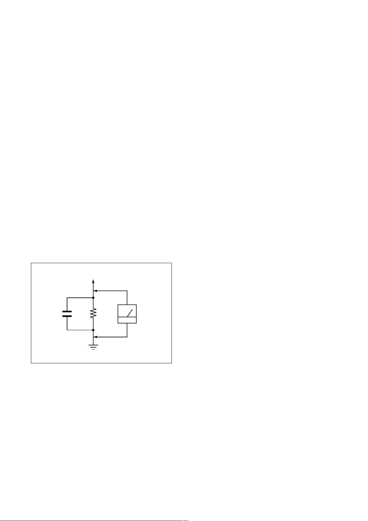
Leakage. Check leakage as described below.
To Exposed Metal
Parts on Set
0.15 µF
1.5 k
Ω
AC
Voltmeter
(0.75 V)
LEAKAGE TEST
The AC leakage from any exposed metal part to earth ground
and from all exposed metal parts to any exposed metal part having a return to chassis, must not exceed 0.5 mA (500 microamperes).
Leakage current can be measured by any one of three methods.
1. A commercial leakage tester, such as the Simpson 229 or
RCA WT-540A. Follow the manufacturers’ instructions to
use these instruments.
2. A battery-operated AC milliammeter. The Data Precision
245 digital multimeter is suitable for this job.
3. Measuring the voltage drop across a resistor by means of a
VOM or battery-operated AC voltmeter. The “limit” indication is 0.75 V, so analog meters must have an accurate lowvoltage scale. The Simpson 250 and Sanwa SH-63Trd are
examples of a passive VOMs that are suitable. Nearly all
battery operated digital multimeters that have a 2 V AC
range are suitable. (See Fig. A)
WARNING!!
NEVER TURN ON THE POWER IN A CONDITION IN
WHICH THE DEGAUSS COIL HAS BEEN REMOVED.
SAFETY-RELATED COMPONENT WARNING!!
COMPONENTS IDENTIFIED BY SHADING AND MARK
¡ ON THE SCHEMATIC DIAGRAMS, EXPLODED
VIEWS AND IN THE PARTS LIST ARE CRITICAL FOR
SAFE OPERATION. REPLACE THESE COMPONENTS
WITH SONY PARTS WHOSE PART NUMBERS APPEAR AS SHOWN IN THIS MANUAL OR IN SUPPLEMENTS PUBLISHED BY SONY. CIRCUIT ADJUSTMENTS THAT ARE CRITICAL FOR SAFE OPERATION
ARE IDENTIFIED IN THIS MANUAL. FOLLOW THESE
PROCEDURES WHENEVER CRITICAL COMPONENTS
ARE REPLACED OR IMPROPER OPERATION IS SUSPECTED.
Earth Ground
Fig. A. Using an AC voltmeter to check AC leakage.
– 2 –
Page 3
POWER SAVING FUNCTION
www.rtv-horvat-dj.hr
If your PC has a VESA DPMS (Video Electronics Standard Association, Display Power
Management Signaling) power management function (energy-saving mode), your monitor will fully
support this function. The monitor has a four-stage power management system.
Stage ON Standby mode Suspend mode OFF mode
Power indicator glows green flashes green/orange flashes green/orange glows orange
Function Monitor operating
Power
consumption
If your PC detects inactivity (no input) it sends an appropriate signal to the monitor to reduce the
power consumption. The power indicator of the monitor changes color to indicate the status change.
If there is still no input, power consumption is further reduced (OFF mode).
Once an input is made at the PC the screen contents are redrawn and full power is restored.
The length of the individual stages is determined by the power management system of the PC. For
detailed information on how energy-saving mode operates refer to the Operating Manual or
Technical Manual of your PC.
The service life of your monitor will be extended if the OFF mode is switched to after
30 minutes at the earliest (setting in screen saver, in your PC's BIOS setup or in the OSD
i
menu).
When the monitor is switched to OFF mode by the power management system a power
consumption of about 3 W is maintained to feed the circuit for redrawing the screen
contents.
To cut off power consumption totally, press the ON/OFF switch on the front of the monitor.
normally
normal
< 140 W
Monitor
is dark
reduced
to < 15 W
Monitor
is dark
reduced
to < 15 W
Monitor
is dark
reduced
to < 3 W
19T2
DIAGNOSIS
The monitor is equipped with a self-diagnosis function. If the monitor recognizes a fault, the screen
display remains dark and the power indicator glows green or flashes orange.
The power indicator glows green
Switch the connected PC off.
Press and hold down the button on the front of the monitor for 2 seconds.
If all four color bars (white, red, green, blue) are shown, the monitor is operating properly. In this
case, check the PC.
If the color bars do not appear, this may be due to a fault in the monitor. Please contact our
customer service center with a description of the problem.
The power indicator flashes orange
Switch the monitor off and on again.
If the power indicator continues to flash orange, there may be a fault in the monitor. Determine the
interval at which the indicator flashes (in seconds) and contact our customer service center with a
description of the problem.
– 3 –
Page 4
19T2
www.rtv-horvat-dj.hr
TIMING SPECIFICATION
MODE AT PRODUCTION
RESOLUTION
CLOCK
— HORIZONTAL —
H-FREQ
H. TOTAL
H. BLK
H. FP
H. SYNC
H. BP
H. ACTIV
— VERTICAL —
V. FREQ (Hz)
V. TOTAL
V. BLK
V. FP
V. SYNC
V. BP
V. ACTIV
— SYNC —
INT(G)
EXT (H/V) /POLARITY
EXT (CS) /POLARITY
INT/NON INT
MODE 1 MODE 2 MODE 3 MODE 4 MODE 5 MODE 6
720 X 400 640 X 480 640 X 480 800 X 600 800 X 600 1024 X 768
28.325 MHz 25.175 MHz 36.000 MHz 56.250 MHz 67.500 MHz 94.500 MHz
31.472 kHz 31.469 kHz 43.269 kHz 53.674 kHz 63.920 kHz 68.677 kHz
usec usec usec usec usec usec
31.774 31.778 23.111 18.631 15.644 14.561
6.355 6.356 5.333 4.409 3.793 3.725
0.635 0.636 1.556 0.569 0.474 0.508
3.813 3.813 1.556 1.138 0.948 1.016
1.906 1.907 2.222 2.702 2.370 2.201
25.419 25.422 17.778 14.222 11.852 10.836
70.094 Hz 59.940 Hz 85.0 Hz 85.061 Hz 100.032 Hz 84.997 Hz
lines lines lines lines lines lines
449 525 509 631 639 808
49 45 29 31 39 40
13 10 1 1 1 1
223333
34 33 25 27 35 36
400 480 480 600 600 768
NO NO NO NO NO NO
YES N/P YES N/N YES N/N YES P/P YES P/P YES P/P
NO NO NO NO NO NO
NON INT NON INT NON INT NON INT NON INT NON INT
MODE AT PRODUCTION
RESOLUTION
CLOCK
— HORIZONTAL —
H-FREQ
H. TOTAL
H. BLK
H. FP
H. SYNC
H. BP
H. ACTIV
— VERTICAL —
V. FREQ (Hz)
V. TOTAL
V. BLK
V. FP
V. SYNC
V. BP
V. ACTIV
— SYNC —
INT(G)
EXT (H/V) /POLARITY
EXT (CS) /POLARITY
INT/NON INT
MODE 7 MODE 8 MODE 9 MODE 10 MODE 11 MODE 12
1024 X 768 1152 X 864 1152 X 864 1280 X 1024 1280 X 1024 1600 X 1200
111.2 MHz 108.000 MHz 146.000 MHz 157.500 MHz 184.900 MHz 229.500 MHz
80.814 kHz 67.500 kHz 93.110 kHz 91.146 kHz 107.002 kHz 106.250 kHz
usec usec usec usec usec usec
12.374 14.815 10.740 10.971 9.346 9.412
3.165 4.148 2.849 2.844 2.423 2.440
0.288 0.593 0.219 0.406 0.173 0.279
1.151 1.185 1.096 1.016 0.692 0.837
1.727 2.370 1.534 1.422 1.558 1.325
9.209 10.667 7.890 8.127 6.923 6.972
99.894 Hz 75.0 Hz 100.1 Hz 85.024 Hz 99.91 Hz 85.000 Hz
lines lines lines lines lines lines
809 900 930 1072 1071 1250
41 36 66 48 47 50
21111 21
3333 33
36 32 52 44 42 46
768 864 864 1024 1024 1200
NO NO NO NO NO NO
YES N/N YES P/P YES N/N YES P/P YES P/P YES P/P
NO NO NO NO NO NO
NON INT NON INT NON INT NON INT NON INT NON INT
2000.2.18 VER.
– 4 –
Page 5

TABLE OF CONTENTS
www.rtv-horvat-dj.hr
Section Title Page
1. GENERAL ................................................................. 1-1
2. DISASSEMBLY
2-1. Cabinet Removal ................................................ 2-1
2-2. Shield (EMI, Video),
Side Cover (L and R) Removal.......................... 2-1
2-3. A Board Removal ............................................... 2-2
2-4. Rear Shield Complete Assy,
D Board Removal ............................................... 2-2
2-5. Service Position .................................................. 2-3
2-6. H Board Removal ............................................... 2-3
2-7. Picture Tube Removal........................................ 2-4
2-8. Harness Location ................................................ 2-5
3. SAFETY RELATED ADJUSTMENT............. 3-1
19T2
4. ADJUSTMENTS ..................................................... 4-1
5. DIAGRAMS
5-1. Block Diagrams .................................................. 5-1
5-2. Frame Schematic Diagram ................................. 5-5
5-3. Circuit Boards Location ..................................... 5-6
5-4. Schematic Diagrams and Printed Wiring
Boards ................................................................. 5-7
(1) Schematic Diagram of A Board ......................... 5-9
(2) Schematic Diagrams of D (a,b,c) Board .... 5-11
(3) Schematic Diagrams of N, H Boards ................. 5-19
5-5. Semiconductors .................................................. 5-21
6. EXPLODED VIEWS
6-1. Chassis ................................................................ 6-1
6-2. Picture Tube........................................................ 6-2
6-3. Packing Materials ............................................... 6-3
7. ELECTRICAL PARTS LIST ............................ 7-1
– 5 –
Page 6
The operating instructions mentioned here are partial abstracts
Color monitor 19T2
A26361-K616-Z100-1-5E19
English - 7
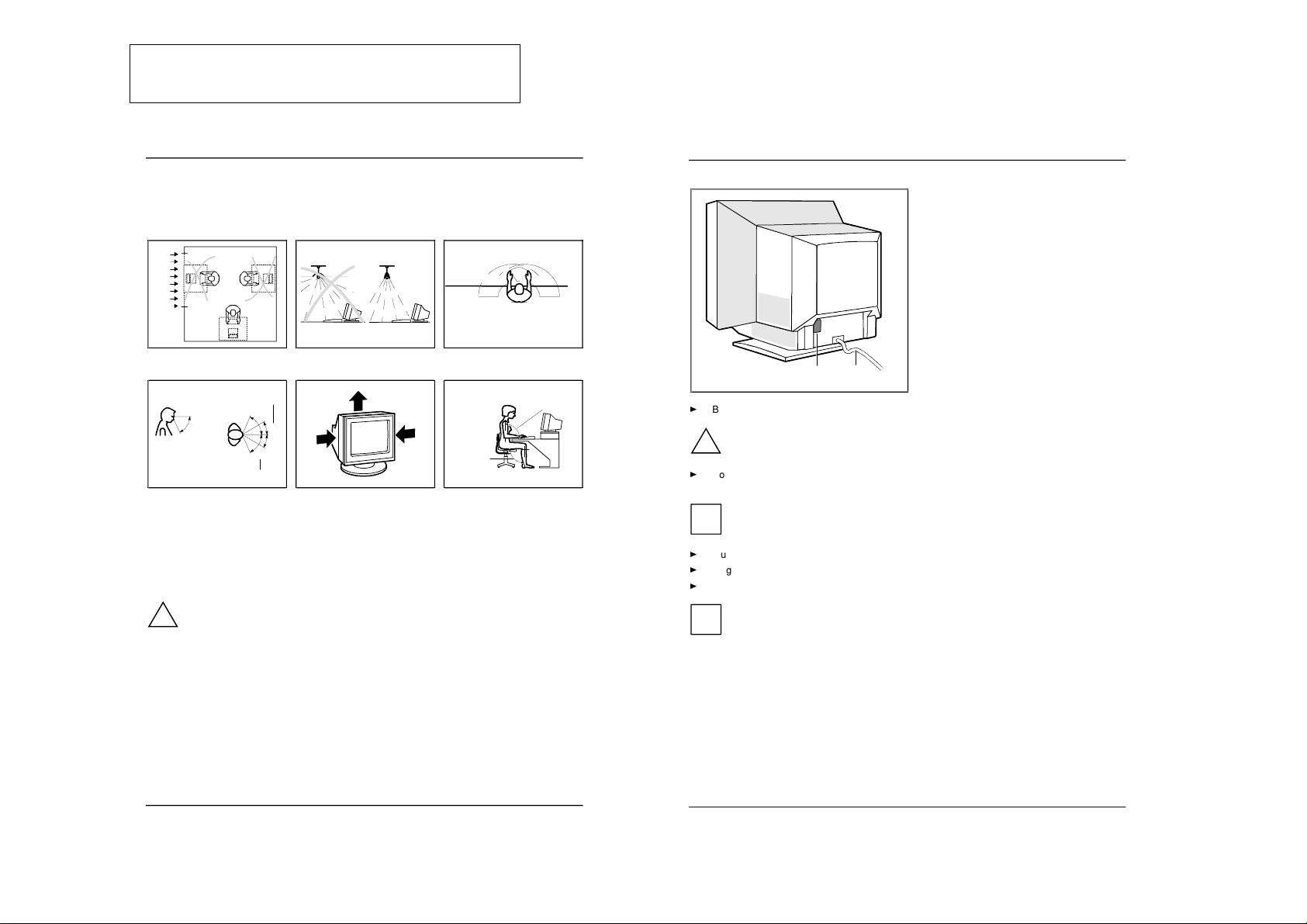
Installing an ergonomic video workstation
Before you set up your equipment you should select a suitable position for working at the monitor.
Please observe the following advices when installing a video workstation.
Window
permissible
reachin
g
sector
600 mm
edge of desk
permissible
reachin
g
sector
600 mm
Avoid direct and reflected glare. Avoid glare from electric
lighting.
Position the keyboard where it
is easiest to reach.
30°
30°
65°
65°
0°
60°
preferable viewin
g
sector
permissible viewin
g
sector
permissible
viewin
g
sector
approx. 90°
and
more
approx. 90°
Position the monitor for
optimum viewing. The viewing
distance to the monitor should
be approximately 50 cm.
Keep ventilated areas clear. Remember to maintain correct
posture.
Connecting the monitor
See your PC's operating manual for details of the ports on the system unit.
!
Please note the information provided in the "Safety" section in the chapter "Important
notes" at the beginning of this manual.
Do not cover the ventilation openings of the monitor.
If you are assembling monitors beside each other, there must be a minimum distance of
30 cm between monitors of the same constructional type, to avoid image distortion. With
different monitors, the distance must be increased, if necessary.
Color monitor 19T2
8 - English
A26361-K616-Z100-1-5E19
1
2
1 = Power connector
2 = Data cable
Be sure that the monitor and the system unit are switched off.
!
The system unit's power plug must be pulled out!
Connect the connector of the data cable to the (active) monitor port on the system unit and
secure the plug-in connection by tightening the safety screws.
i
If your system unit has two monitor ports ("onboard" screen controller and separate
graphics card), the monitor port for the separate graphics card is usually active.
Plug the power cable supplied into the power connector (1) of the monitor.
Plug the power connector of the monitor into a properly grounded power outlet.
Plug the power connector of the system unit into a properly grounded power outlet.
i
When you start working with your monitor for the first time you should install the
appropriate graphics drivers for your application software. Details of how to do this are
provided in the documentation on your screen controller/the associated driver software.
www.rtv-horvat-dj.hr
from the Operating Instruction Manual. The page numbers of
the Operating Instruction Manual remain as in the manual.
SECTION 1
GENERAL
1-1
Page 7
Color monitor 19T2
A26361-K616-Z100-1-5E19
English - 9
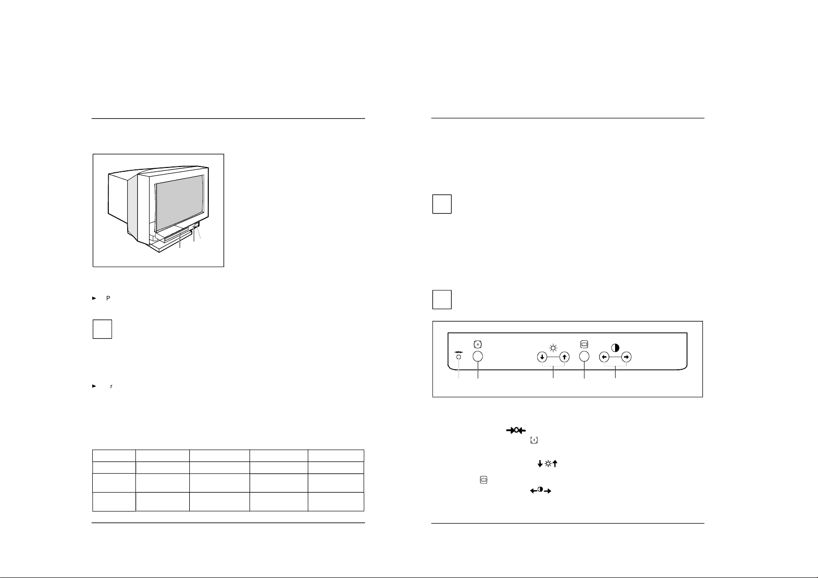
Operation of the monitor
1
2
3
1 = Control panel with buttons for screen
setting
2 = Power indicator
3 = ON/OFF switch
Switching the monitor on
Press the ON/OFF switch (3).
The power indicator (2) lights up green when the system unit is turned on.
i
If your PC has a power management function (energy-saving mode), you should read the
"Notes on power management" of the monitor in this chapter.
When you start your system, several mode changes will usually be carried out when
various programs are called automatically (different settings for resolution and image
refresh rate). Do not be confused by the unusual displays. They are not error messages.
Switching the monitor off
Press the ON/OFF switch (3).
The power indicator (2) is dark.
Notes on power management
If your PC has a VESA DPMS (Video Electronics Standard Association, Display Power
Management Signaling) power management function (energy-saving mode), your monitor will fully
support this function. The monitor has a four-stage power management system.
Stage ON Standby mode Suspend mode OFF mode
Power indicator glows green flashes green/orange flashes green/orange glows orange
Function Monitor operating
normally
Monitor
is dark
Monitor
is dark
Monitor
is dark
Power
consumption
normal
< 140 W
reduced
to < 15 W
reduced
to < 15 W
reduced
to < 3 W
Color monitor 19T2
10 - English
A26361-K616-Z100-1-5E19
If your PC detects inactivity (no input) it sends an appropriate signal to the monitor to reduce the
power consumption. The power indicator of the monitor changes color to indicate the status change.
If there is still no input, power consumption is further reduced (OFF mode).
Once an input is made at the PC the screen contents are redrawn and full power is restored.
The length of the individual stages is determined by the power management system of the PC. For
detailed information on how energy-saving mode operates refer to the Operating Manual or
Technical Manual of your PC.
i
The service life of your monitor will be extended if the OFF mode is switched to after
30 minutes at the earliest (setting in screen saver, in your PC's BIOS setup or in the OSD
menu).
When the monitor is switched to OFF mode by the power management system a power
consumption of about 3 W is maintained to feed the circuit for redrawing the screen
contents.
To cut off power consumption totally, press the ON/OFF switch on the front of the monitor.
Changing the monitor settings
With the buttons on the control panel, you can change the monitor settings. Most settings are
carried out via an integrated OSD menu (On-Screen Display).
i
The OSD menu is available in different languages. The English menu names are used in
the following description (default setting). How you set a different language for the OSD
menu is described in the section "Setting the language for the OSD menu (LANGUAGE)".
12
4
5
3
1 = Factory settings button
2 = Picture size/position button
(automatic setting)
3 = Brightness/arrow up/down button
4 = Menu button
5 = Contrast/arrow left/right button
The factory settings button
(1) is used to reset the values to the factory settings.
With the picture size/position button
(2) the screen display can be automatically adjusted so that
it fits on the screen. This function is especially intended for computers with graphic user interfaces
(software) which fills the entire screen.
The brightness/arrow up/down buttons
(3) are used to set the brightness and to operate the
OSD menu.
The menu button
(4) switches the OSD menu on and off.
The contrast/arrow left/right buttons
(5) are used to set the contrast and to operate the OSD
menu.
www.rtv-horvat-dj.hr
1-2
Page 8
Color monitor 19T2
A26361-K616-Z100-1-5E19
English - 11
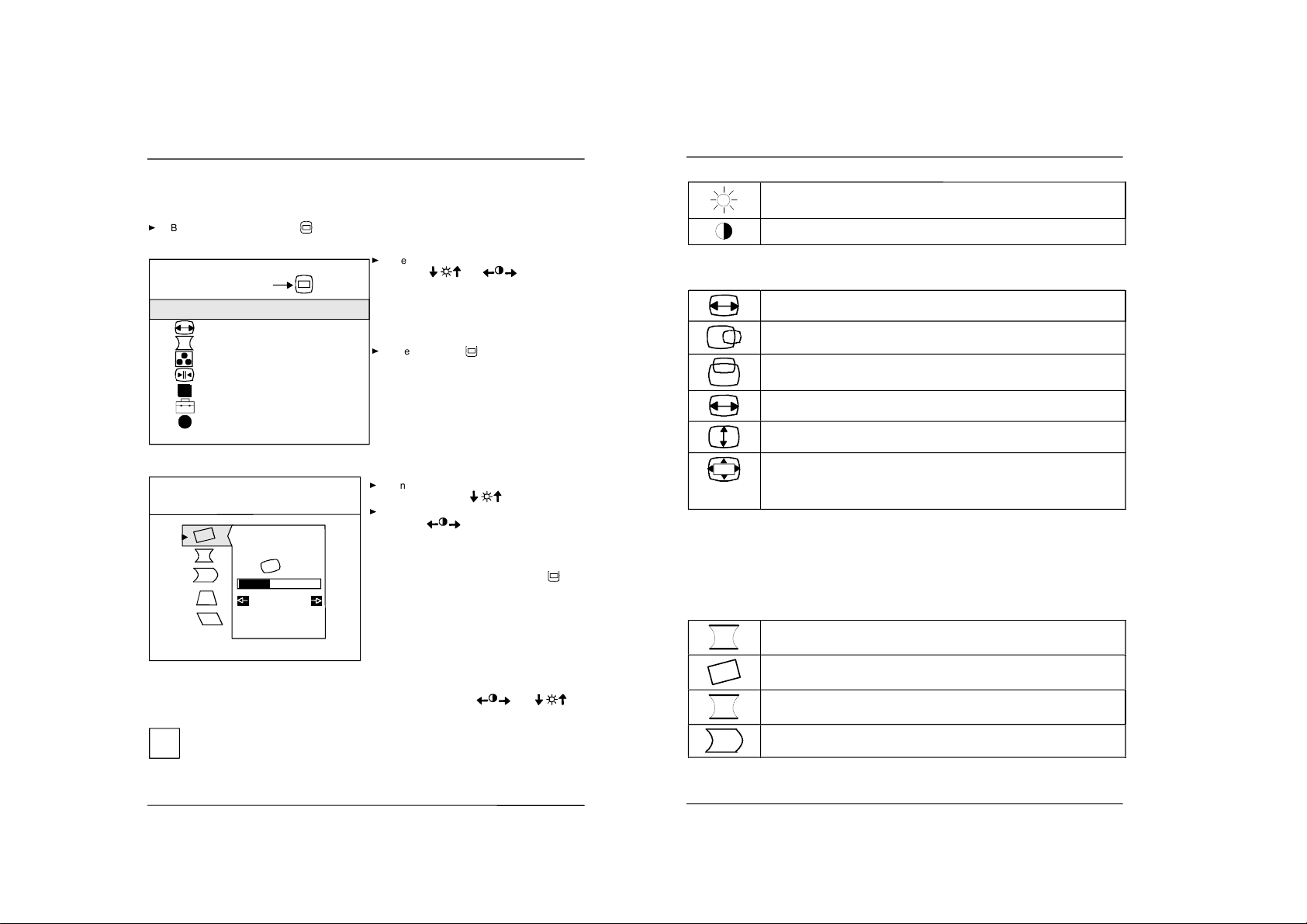
Operating the OSD menu
To set the OSD menu, perform the following steps:
Briefly press the Menu button
to activate the OSD menu.
The main menu appears on the screen with icons for the setting functions.
A
OK
EXIT
SIZE/CENTER
GEOMETRY
COLOR
CONVERGENCE
LANGUAGE
OPTION
HELP
MENU
?
Select the desired symbol with the arrow
buttons
and
, e. g.
GEOMETRY
.
(If you wish to exit the OSD menu, select
EXIT
.)
The selected symbol has a colored
marking.
Press the Menu button to display the
appropriate options window.
Depending on what options window is involved (here:
GEOMETRY
.), further icons are offered.
26
GEOMETRY
If necessary, select a different symbol with
the arrow buttons
.
Make the required setting using the arrow
buttons
.
All changes are stored automatically.
The OSD menu disappears after approx.
30 seconds. The OSD menu can be hidden
beforehand by pressing the menu button
(possibly several times).
Adjusting the contrast and brightness
The contrast and brightness can be adjusted directly with the arrow buttons
and
of
the control panel when the OSD menu is hidden. The set values are saved for all input signals.
i
You will increase the life of your screen if you adjust the contrast and brightness to
medium.
In the setting window for contrast and brightness, the horizontal frequency and refresh
rate of the current input signal are displayed as additional information.
Color monitor 19T2
12 - English
A26361-K616-Z100-1-5E19
Setting the brightness of the background
Setting the contrast between the foreground and background
Setting picture position and size (SIZE/CENTER)
The set values for the picture position and size are only saved for the current input signal.
Calling the SIZE/CENTER setting window
Horizontal picture position (H CENTER): Shifting the picture to the left or to the
right
Vertical picture position (V CENTER): Shifting the picture down or up
Horizontal picture size (H SIZE): Making the picture narrower or wider
Vertical picture size (V SIZE): Making the picture shorter or longer
Proportional picture size (ZOOM): Increasing or reducing picture size while
retaining the side ratios
The picture zoom adjustment will stop as soon as either the horizontal or vertical
size reaches its maximum or minimum value.
Setting the picture geometry (GEOMETRY)
Tilt distortion must be set when the screen display is not axially symmetrical.
Pincushion distortion is when the sides of the screen display are bent inward or outward. Trapezoid
distortion is when the top or bottom of the screen display is too wide or too narrow. Parallelogram
distortion means that the sides of the picture bend to the left or right.
The set value for the picture rotation is saved for all input signals. All other values of the picture
geometry are only saved for the current input signal.
Calling the GEOMETRY options window
Picture rotation (ROTATION): Rotating the picture in a clockwise or counterclockwise direction
Vertical pincushion distortion (PINCUSHION): Bending the right and left side
inward or outward
Asymmetrical pincushion distortion (PIN BALANCE): adjusting right and left side
symmetrically
www.rtv-horvat-dj.hr
1-3
Page 9
Color monitor 19T2
A26361-K616-Z100-1-5E19
English - 13
Trapezoid distortion (
KEYSTONE
): Making the bottom edge narrower and the top
edge wider or making the top edge narrower and the bottom edge wider
Parallelogram distortion (
KEY BALANCE
): Reducing the angle of the left and right
sides
Setting color temperature and colors (COLOR)
The "warmth" of the screen colors is set using the color temperature. The monitor has two fixed
color temperatures (K = Kelvin). In addition, a user-defined fine calibration of the colors can also be
carried out.
If you have reached the maximum value for one of the primary colors (red, green, blue), this will
affect the settings for the other primary colors.
The set value for the color setting is saved for all input signals.
Calling the
COLOR
setting window
9300 K
Selecting color temperature 9300 K (more blue)
5000 K
Selecting color temperature 5000 K (more red)
Setting a user-defined color temperature
(0 = more red, 100 = more blue)
sRGB
Setting the sRGB color mode
The sRGB color mode can only be used when your PC and other connected
devices (e.g. printer) are sRGB-compatible.
The sRGB color mode is an industry standard protocol designed to correlate the
displayed and printed colors of sRGB compliant devices. In order to display the
sRGB colors correctly ( = 2.2; 6500 K), you must set your PC to the sRGB profile
and adjust the brightness and contrast to the values shown in the menu.
Setting convergence (CONVERGENCE)
If objects on the screen have red or blue shadows, the vertical or horizontal convergence of the
monitor is incorrectly adjusted.
Calling the
CONVERGENCE
setting window
Horizontal convergence (
H CONVERGENCE
): Shifting red and blue shadows to the
right/to the left
Vertical convergence (
V CONVERGENCE)
: Shifting red and blue shadows up or
down
Color monitor 19T2
14 - English
A26361-K616-Z100-1-5E19
Setting language for the OSD menu (LANGUAGE)
A
Setting language for the OSD menu
You can choose from English (default setting), German, French, Spanish, Italian,
Swedish, Dutch, Russian and Japanese.
Setting monitor options (OPTION)
You can degauss the monitor in the settings window OPTION, you can set the Moiré correction,
change the OSD position, lock/release the buttons for monitor settings and restore original monitor
colors.
The set value for the Moiré correction is only saved for the current input signal. The other values are
independent of a change in the input signal.
Calling the OPTION setting window
Degaussing the monitor (MANUAL DEGAUSS)
The monitor is degaussed every time you switch it on. When color shifts occur in
the screen display due to the influence of magnetic fields, the screen must be
degaussed manually.
Press the button
. The monitor is degaussed for approximately 3 seconds.
If the monitor is to be degaussed a second time, please wait approximately
20 minutes before executing the function again.
Correcting the Moiré effect (MOIRE ADJUST)
If the picture you see on screen has light and dark stripes or appears dull and
blurred, this may be due to what is known as the moiré effect. This effect usually
has physical causes, being triggered by interference between the pixels in the
matrix and the video signal. The intensity of the moiré effect is dependent on the
screen resolution and horizontal frequency.
Setting horizontal position of the OSD menu (OSD H POSITION)
You can change the OSD position, for example, when you want to adjust the
picture behind an OSD window.
Setting vertical position of the OSD menu (OSD V POSITION)
You can change the OSD position, for example, when you want to adjust the
picture behind an OSD window.
Lock/unlock buttons for adjusting the monitor (CONTROL LOCK)
With this option all buttons on the front of the monitor (with the exception of the
menu button
and the on/off switch) can be locked and unlocked again.
OFF = unlocked
ON = locked
If ON has been selected, only the symbols OPTION or EXIT can be selected in the
main menu. If - with the OSD menu hidden - a button other than the menu button
or the on/off switch is pressed, the key symbol appears on the screen.
www.rtv-horvat-dj.hr
1-4
Page 10
Color monitor 19T2
A26361-K616-Z100-1-5E19
English - 15
Restore original monitor colors (
COLOR RETURN
)
After a number of years of operation the color brightness of your monitor may
decrease slowly. With this function you can reset the monitor colors to
manufacturer's default values. (Due to the natural aging process this function may
no longer work after a certain period of time.)
Prior to being able to use this function, the monitor must have been in standard
operation for at least 30 minutes (power indicator is green). If the monitor changes
over into energy saving mode, switch it back to normal mode and wait for
30 minutes. You may have to change the energy saving settings of your computer
in order to keep the monitor in standard operating setting for 30 minutes. If the
monitor is not ready, a respective message will appear.
Press the button
. While the original screen colors are being restored the
screen remains dark. This process takes about 2 seconds.
Open Help menu (HELP)
The most frequent questions and problems are covered here.
?
Calling the
HELP
window
RETURN TO MAIN MENU
Return to main menu
RECOMMENDED RESOLUTION
Recommended resolution:
1280 x 1024 at 85 Hz
FLICKER
Flickering:
Display of current refresh rate and reference to recommended
refresh rate >75 Hz
THIN HORIZONTAL LINE
Thin horizontal line:
There is no malfunction.
DISTORTED SHAPE
Picture distorted:
Setting the picture geometry (
GEOMETRY
)
OUT OF FOCUS
Picture is blurred:
Setting convergence (
CONVERGENCE
)
DISCOLORATION
Discoloration:
Check data cable
degauss monitor (
MANUAL DEGAUSS
)
Activating the factory settings
With the factory settings button on the front of the monitor, either the adjustment of a selected
function can be specifically reset to the factory setting, all settings for the current input signal can be
reset or all input signals reset.
Resetting a selected function to the factory setting
Select the function in the OSD menu to be reset.
Press the factory settings button
.
Color monitor 19T2
16 - English
A26361-K616-Z100-1-5E19
Resetting all settings for the current input signal
Press - with the OSD menu hidden - the factory settings button
.
All settings for the current input signal are reset.
i
With this method those settings are not reset which are not influenced by a change in the
input signal (language and position of the OSD menu, color setting, locking of the buttons
for monitor adjustment).
Resetting all settings for all input signals
Press and hold down the factory settings button
- with the OSD menu hidden - for at
least 2 seconds.
All settings including brightness and contrast are reset to the factory values.
Notes on ergonomic color adjustment
If you select colors for the display in your application programs, take note of the information below.
The primary colors blue and red on a dark background do not produce the minimum required
contrast of 3:1 and are therefore not suitable for continuous text and data entry.
When using several colors for characters and background and giving the primary colors full
modulation, you can obtain very suitable color combinations (see the following table):
Background Characters
black white purple blue cyan green yellow red
black + + - + + + -
white + + + - - - +
purple + + -----
blue - + - + - + -
cyan + - - + - - -
green + - - + - - -
yellow + - + + - - +
red -+----+
+ Color combination very suitable
- Color combination not suitable because color locations are too close together, thin characters
are not identifiable or rigorous focusing is demanded of the human eye.
www.rtv-horvat-dj.hr
1-5
Page 11
Color monitor 19T2
A26361-K616-Z100-1-5E19
English - 17
Technical data
Dimensions and weight
CRT: 46 cm (19")
Visible diagonals: 46 cm
Dot pitch: 0.24 - 0.25 mm (slot mask)
Maximal resolution: 1600 x 1200 pixels
Preset display area: 352 mm x 264 mm
Dimensions (W x H x D): 449 mm x 463 mm x 463 mm
Weight: 26 kg
Accessories: Power cable (1.8 m)
Storable display modes: 25 (10 of which are preset)
Electrical data
Video: analog, positive, 0.7 Vpp, 75 Ohm
Synchronization: Separate Sync. TTL
Composite Sync. TTL/ Sync. on Green
Horizontal frequency: 30 kHz .... 107 kHz (multi-scanning)
Refresh rate: 48 Hz .... 120 Hz
Maximum pixel rate: 230 MHz
Power supply: 180 V -264 V, 50 Hz - 60 Hz 3 Hz,
< 1 A max. at 220 V
Power consumption:
(see power management):
< 145 W (ON, Normal mode)
< 15 W (Standby mode)
< 15 W (Suspend mode)
< 3 W (OFF mode)
Environmental conditions
Environment class 3K2, IEC 721
Rated range of operation: 15 °C .... 35 °C
Humidity: 20 % .... 85 %
Limit range of operation: 5 °C .... 40 °C
Humidity: 20 % .... 85 %
Condensation must be avoided.
Color monitor 19T2
18 - English
A26361-K616-Z100-1-5E19
VESA-DDC-compatible VGA interface
Your monitor is equipped with a VESA-DDC-compatible VGA interface. VESA-DDC (Video
Electronics Standard Association, Display Data Channel) is used as the communications interface
between the monitor and the PC. If your PC is equipped with a VESA-DDC-compatible VGA
interface, it can automatically read the data for ensuring optimum operation from your monitor and
select the appropriate settings.
i
If the monitor 19T2 is not yet displayed in the list of monitors, you can select one of the
following monitors instead:
Siemens or Siemens Nixdorf MCM 21T1, MCM 2106, MCM 212V
Preset operating modes
i
The display position and size have been set to optimum values at the factory for the
operating modes listed above. Depending on the screen controller used, it may be
necessary to adjust the display position and size. In this case, you can change and save
the settings (see "Operation of the monitor").
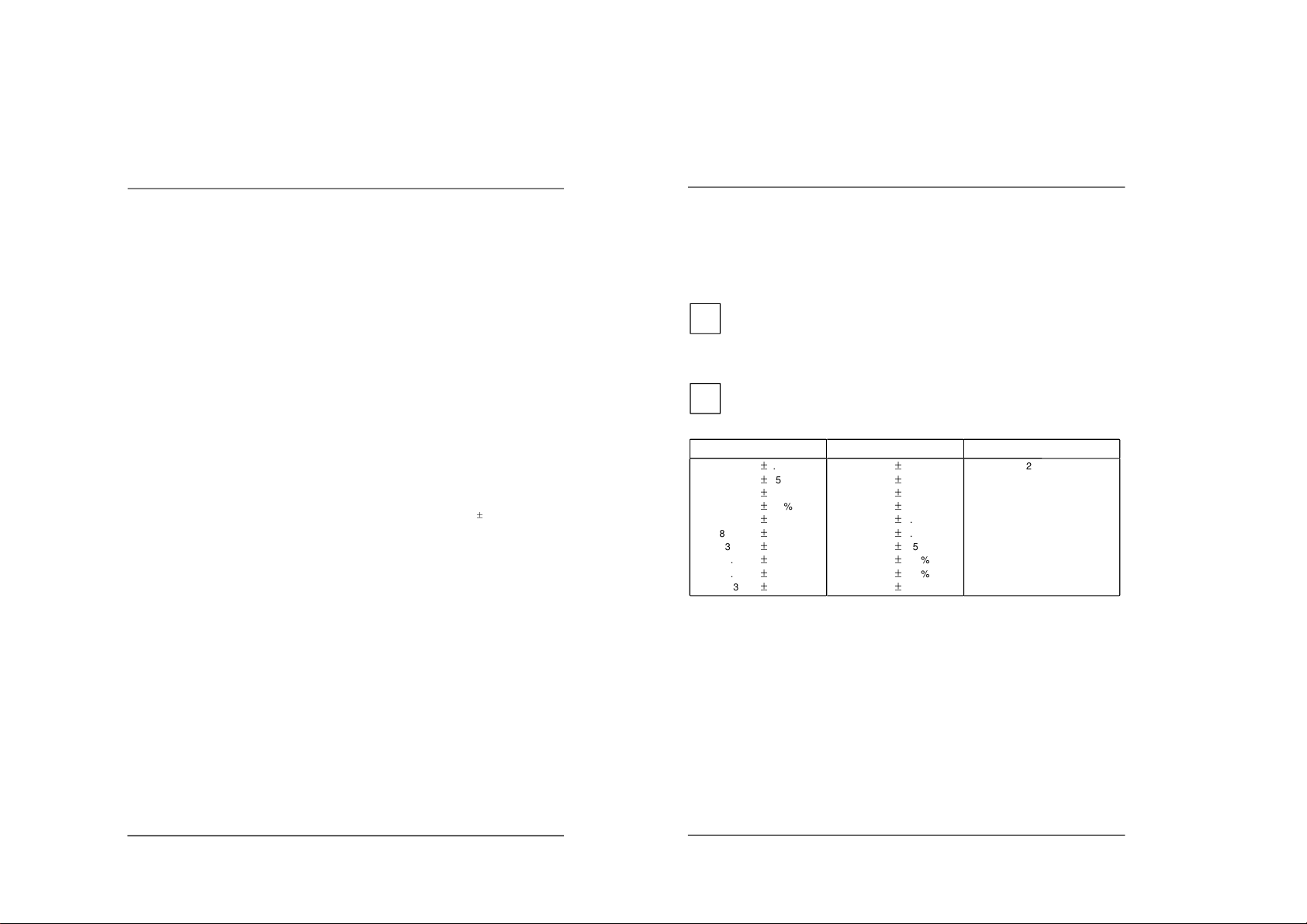
Horizontal frequency Refresh rate Screen resolution
31.5 kHz 0.5 %
31.5 kHz
0.5 %
53.7 kHz
0.5 %
63.9 kHz
0.5 %
68.7 kHz
0.5 %
80.8 kHz
0.5 %
93.1 kHz
0.5 %
91.1 kHz
0.5 %
107.0 kHz
0.5 %
106.3 kHz
0.5 %
70 Hz
0.5 %
60 Hz
0.5 %
85 Hz
0.5 %
100 Hz
0.5 %
85 Hz
0.5 %
100 Hz
0.5 %
100 Hz
0.5 %
85 Hz
0.5 %
100 Hz
0.5 %
85 Hz
0.5 %
720 x 400
640 x 480
800 x 600
800 x 600
1024 x 768
1024 x 768
1152 x 864
1280 x 1024
1280 x 1024
1600 x 1200
For ergonomic reasons we recommend a refresh rate of at least 75 Hz and a maximum resolution of
1024 x 1280 pixels.
www.rtv-horvat-dj.hr
1-6
Page 12
Color monitor 19T2
A26361-K616-Z100-1-5E19
English - 19
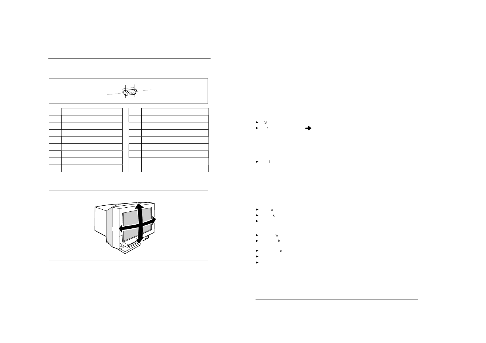
Pin assignment D-SUB (15-pin)
1
5
6
10
11
15
Pin Meaning Pin Meaning
1 Video input red 9 + 5 V
2 Video input green / Sync. on green 10 Logic ground
3 Video input blue 11 Monitor ground
4 Monitor ground 12 Bi-directional Data (SDA)
5 DDC ground 13 H. sync
6 Red video ground 14 V. sync
7 Green video ground 15 Data Clock (SCL)
8 Blue video ground
Tilting and turning area
15°
5°
90°
90°
Color monitor 19T2
20 - English
A26361-K616-Z100-1-5E19
Error handling
Should an error occur, first check the following points. If the distortion is still not eliminated, the
monitor should, if possible, be checked on another PC.
Self-diagnosis
The monitor is equipped with a self-diagnosis function. If the monitor recognizes a fault, the screen
display remains dark and the power indicator glows green or flashes orange.
The power indicator glows green
Switch the connected PC off.
Press and hold down the
button on the front of the monitor for 2 seconds.
If all four color bars (white, red, green, blue) are shown, the monitor is operating properly. In this
case, check the PC.
If the color bars do not appear, this may be due to a fault in the monitor. Please contact our
customer service center with a description of the problem.
The power indicator flashes orange
Switch the monitor off and on again.
If the power indicator continues to flash orange, there may be a fault in the monitor. Determine the
interval at which the indicator flashes (in seconds) and contact our customer service center with a
description of the problem.
Possible malfunctions
If you cannot solve the problem, contact our customer service center.
The screen is blank (power indicator does not light)
Check whether the monitor is switched on.
Check whether the power cable on the monitor is connected correctly.
Check whether the mains socket is live.
The screen is blank (power indicator lights)
Check whether the system unit is switched on.
Check whether the data cable for the monitor is correctly attached to the monitor and the
monitor port on the system unit.
Check whether the monitor connection of the system unit used is active.
Press any key on the PC keyboard - the PC may be in energy saving mode.
Change the brightness and/or the contrast; the monitor may be adjusted to the maximum dark
setting.
www.rtv-horvat-dj.hr
1-7
Page 13
Color monitor 19T2
A26361-K616-Z100-1-5E19
English - 21
Two fine horizontal lines (wires) are visible
i
Your monitor is equipped with a Trinitron picture tube, which enables more light to reach
the screen with a vertical slot mask, and therefore produces more intense colors. The
thin lines visible with a white background are shadows of the damper wires, which
stabilize the vertical slot mask. They are characteristic of picture tubes with a vertical slot
mask. There is no malfunction.
The screen display is too small or not centered
The monitor recognizes an undefined mode (see "Technical data").
i
To display the current mode (horizontal frequency and refresh rate), press the
or
buttons.
Press the picture size/position button
to automatically adjust the screen display.
Correctly adjust the picture size and position with the OSD menu (see "Operation of the
monitor", section "Setting picture position and size (SIZE/CENTER)").
Picture geometry is defective
Correctly adjust the picture geometry with the OSD menu (see "Operation of the monitor",
section "Setting picture geometry (GEOMETRY)").
Colors are impure or shifted
Degauss the monitor (see "Operation of the monitor", section "Setting monitor options
(OPTION)").
Set the convergence (see "Operation of the monitor", section "Setting convergence
(CONVERGENCE)").
White does not look white
Set the color temperature (see "Operation of the monitor", section "Setting color temperature
and colors (COLOR)").
Screen display has lines, is dull or blurred
Set the brightness and contrast (see "Operation of the monitor").
Degauss the monitor (see "Operation of the monitor", section "Setting monitor options
(OPTION)").
Set the convergence and reduce the Moiré correction (see "Operation of the monitor", section
"Setting monitor options (OPTION)").
The screen display is flickering
Set an ergonomic refresh rate ( 75 Hz) using the PC software (see documentation for your PC
or your screen controller/graphics card).
Monitor adjustment buttons do not react
The buttons have probably been locked with the OSD menu.
Unlock the monitor adjustment buttons (see "Operation of the monitor", section "Setting monitor
options (OPTION)").
Color monitor 19T2
22 - English
A26361-K616-Z100-1-5E19
A humming noise is heard after switch-on
The monitor is degaussed every time you switch it on. This produces the humming noise. There is
no malfunction.
Error messages on the screen
MONITOR IS WORKING OUT OF THE SCAN RANGE
The input signal (horizontal frequency and refresh rate) does not correspond to the technical
monitor data.
Adjust the video frequency range using the PC software (see documentation for your PC or
your screen controller/graphics card).
MONITOR IS WORKING - CHECK SIGNAL CABLE
The monitor does not recognize an input signal.
Check whether the system unit is switched on.
Check whether the data cable for the monitor is correctly attached to the monitor and the
monitor port on the system unit.
Check whether the power cable on the system unit is connected to a power outlet with earthing
contact.
www.rtv-horvat-dj.hr
1-8
Page 14
19T2
www.rtv-horvat-dj.hr
SECTION 2
DISASSEMBLY
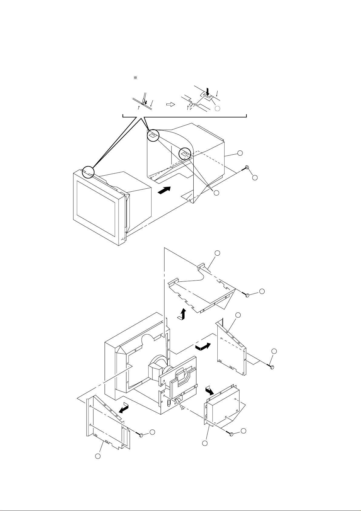
2-1. CABINET REMOVAL
Push in the tip of a screwdriver about
5mm to unlock the two claws.
Cabinet
Bezel assembly
Bezel assembly
Cabinet
1
Two claws
1
Two claws
3
Cabinet
2
Two screws
(+BVTP 4 x 16)
2-2. SHIELD (EMI, VIDEO),
SIDE COVER (L and R) REMOVAL
2
EMI shield (Upper)
4
Side cover (L)
1
Three screws
(+BVTT 4 x 8)
3
Two screws
(+BVTT 4 x 8)
5
Four screws
(+BVTT 4 x 8)
8
Video shield
6
Side cover (R)
2-1
7
Three screws
(+BVTT 4 x 8)
Page 15
2-3. A BOARD REMOVAL
www.rtv-horvat-dj.hr
CN303
CN309
CN306
CN311
CN305
4
A board
1
Screw
(+BVTT 4 x 8)
2
Cable stopper
3
Three screws
(+BVTT 3 x 8)
19T2
2-4. REAR SHIELD COMPLETE ASSY,
D BOARD REMOVAL
Referring to 2-3, disconnect five connectors
(CN303, CN305, CN306, CN309 and CN311).
A
N board
A
7
Two screws
(+BVTP 3 x 8)
CN303
6
Screw
(+P 3.5 x 20)
5
Three screws
(+BVTT 3 x 8)
8
D board
CN601
CN600
4
Rear shield
complete assembly
3
Widening the chassis toward
the direction A , disengage
two claws.
1
Cable cover
2-2
2
Screw
(+BVTT 4 x 8)
Page 16

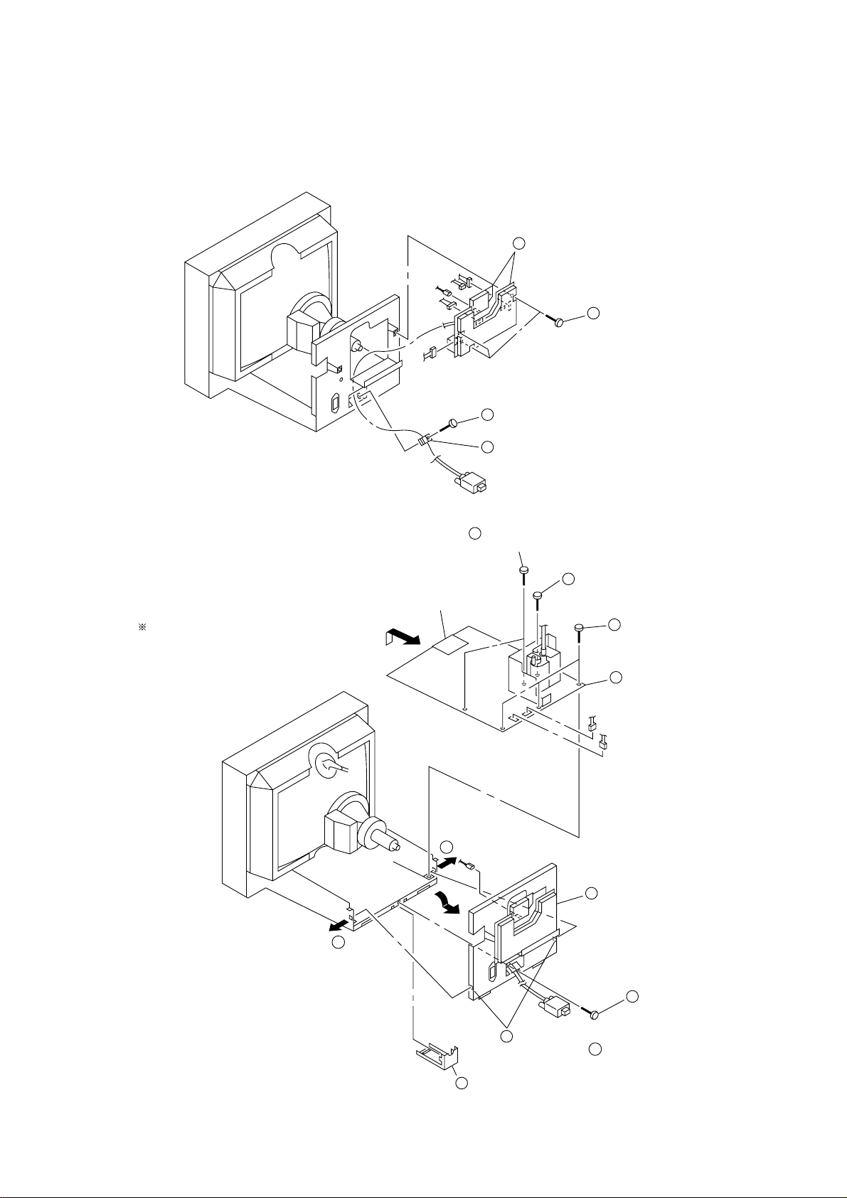
19T2
www.rtv-horvat-dj.hr
2-5. SERVICE POSITION
A board
1
3
D board
2-6. H BOARD REMOVAL
1
Before removing the bezel assembly,
secure the picture tube shield at the
positions shown with the arrow (diagonal
two places) to prevent the picture tube
from falling. (Use the screws +BVTT4x8
that fix shield.)
Picture tube shield
AC inlet
5
H board
2
2
Four screws
(Tapping screw(5))
4
Two screws
(+ BVTP 3 x 8)
CN801
3
Bezel assembl
y
2-3
Page 17

2-7. PICTURE TUBE REMOVAL
www.rtv-horvat-dj.hr
1
Anode cap
CN11
4
Four screws
(Tapping screw (5))
2pin
CN1
3
7
Three connectors
Neck assembly
2
A board
19T2
8
Deflection yoke
6
Picture tube
5
Bezel assembly
CN801
• REMOVAL OF ANODE-CAP
NOTE: Short circuit the anode of the picture tube and the anode cap to the metal chassis, CRT shield or carbon painted on the CRT, after
removing the anode.
• REMOVING PROCEDURES
c
b
a
Anode Button
1 Turn up one side of the rubber cap in
the direction indicated by the arrow a.
2 Using a thumb pull up the rubber cap
firmly in the direction indicated by the
arrow b.
• HOW TO HANDLE AN ANODE-CAP
1 Don’t scratch the surface of anode-caps with sharp shaped
material!
2 Don’t press the rubber hardly not to damage inside of anode-
caps!
A material fitting called as shatter-hook terminal is built in the
rubber.
3 Don’t turn the foot of rubber over hardly!
The shatter-hook terminal will stick out or damage the rubber.
3 When one side of the rubber cap is
separated from the anode button, the
anode-cap can be removed by turning
up the rubber cap and pulling up it in the
direction of the arrow c.
2-4
Page 18

19T2
www.rtv-horvat-dj.hr
2-8. HARNESS LOCATION
H board
D board
CN1003
CN702
CN2001
CN1
CN1004
CN603
CN11
CN1002
Picture tube
Degaussing coil
N board
CN701
Side cover (L)
CN501
CN904
CN600
CN601
FBT
AC inlet
Rear shield
CN313
CN302
CN315
CN309
CN301
CN303
CN310
CN306
CN311
A board
2-5
Page 19

SECTION 3
www.rtv-horvat-dj.hr
SAFETY RELATED ADJUSTMENT
19T2
When replacing or repairing parts in the table shown below, the following operational checks must be performed
as a safety precaution against X-rays emissions from the
unit.
Part Replaced ([)
HV ADJ
HV Regulator
Circuit Check
HV Protector
Circuit Check
Beam Current
Protector Circuit
Check
* Confirm one minute after turning on the power.
a) High Voltage Adjustment
1) Adjust the high voltage 27.0 kV ± 0.2 kV by the
RV901.
Note: Perform high voltage adjustment after the rough adjust-
ments were completed on PICTURE size and FOCUS.
D Board T901(FBT), IC901,
D Board T901(FBT), R917,
D Board R933, R932, R921,
RV901
Part Replaced (])
R924, R925, RV901
• Mounted D board
R918, R923, R920,
R919, R1004, C920,
D911, R912,
• Mounted D board
R1006, D915, D917,
IC901, T901(FBT)
• Mounted D board
b) High Voltage Hold-Down Function Check
1) Apply the voltage 21.1 VDC between D912 cathode and GND shown on the right to confirm that the
RASTER will vanish.
c) Beam Current Protector Function Check
1) Connect Power Supply 1.68 mA to between pin 11 ~
GND of FBT (T901).
2) Confirm that voltage on C922 (ABL DET.) is less
than 2.25 V or monitor will shut down.
d) OCP Function Check
1) Turn ON Power Supply.
2) Connect 3 Z/20 W of Resistor between +200 V Line
and GND, and make sure that OCP will function
(Power LED will vanish and the sound “chi,chi,chi
will be heard.), and cut-off AC input promptly.
e) Power Supply Operation Check
1) Apply AC100 V to the D Board.
2) Make sure that the line voltage at the both ends of
C621 is 200 ± 3.0 VDC.
+ 0.00
– 0.05
3-1
Page 20

19T2
www.rtv-horvat-dj.hr
SECTION 4
ADJUSTMENTS
• Landing Rough Adjustment
1. Enter the full white signal. (or the full black dots signal).
2. Adjust the contrast to the maximum.
3. Make the screen monogreen.
Note: Off the outputs from R ch and B ch of SG.
4. Reverse the DY, and adjust coarsely the purity magnet so
that a green raster positions in the center of screen.
5. Moving the DY forward, adjust so that an entire screen becomes monogreen.
6. Adjust the tilt of DY. For the TILT component, use TLV of
DY.
Note: Observe the following adjustment conditions:
“TILT” = 0
“VPIN SAW TOP” = 0
“VPIN SAW BTM” = 0
7. Lock the DY lightly with a locking fitting.
• Landing Fine Adjustment
<Landing adjustment conditions>
a) Brightness: 1/3 Σ IK (Σ IK = 750 µA)
b) Aging time: 2 hours or more.
c) Atmospheric temperature: 25 °C
d) magnetic Field:
BH = 0 ± 2 µT
BV = 45 ± 2 µT (U/C, AEP)
–55 ± 2 µT (South Hemisphere)
–10 ± 2 µT (Equator destination)
e) Adjustment point:
1-inch inside from the edge of CRT effective tube surface.
1. Put the set inside the Helmholtz coil.
2. Set the TLH plate to “0” position.
3. Set the purity magnet of Neck Assy in “0” position, and lock
with a white pen.
4. Set “VPIN SAW TOP” and “VPIN SAW BTM” to “0” position.
5. Receive an image of the monogreen signal.
6. Degauss the CRT and iron shield parts.
Note: Iron bottom chassis and EMI shield should be degaussed
before assembling the chassis.
7. Perform auto degaussing.
8. Attach the wobbling coil to the designated part of the CRT
neck.
9. Attach the sensor of the landing adjustment unit on the CRT
surface.
10. Adjust the DY position and purity, and the DY tilt.
Note: Use purity magnet on the DY.
11. Fasten DY with screw.
Note: Torque 22 ± 2 kg•cm (2.2 ± 0.2 Nm).
12. Perform auto degaussing.
13. Using two wedges, adjust vertical pins so as to attain a=b as
shown below. Further, insert two wedges as shown in the
right figure, and lock the center so that DY does not fluctuate
horizontally.
Note: Insert wedges completely so that the DY does not move.
14. If the corner landing is out of the specification, use the landing magnet so as to satisfy the specification.
<Specification>
a) Green x ± 4 x ± 7.5 x ± 4
x ± 4 x ± 7.5 x ± 4
x ± 4 x ± 7.5 x ± 4
[X] is bias value for a difference caused depending on
whether the EMI shield and rear cover are present or not.
J Models : x = 1.5 [µm]
b) Difference between Green and Red, and between Green
and Blue.
± 5 ± 5 ± 5
± 5 ± 5 ± 5
± 5 ± 5 ± 5 [µm]
c) Difference Red and Blue.
± 8 ± 8 ± 8
± 8 ± 7 ± 8
± 8 ± 8 ± 8 [µm]
Note:
(1) Do not paste more than two magnets on one corner.
(2) Magnets will be placed in a range of 80 ~ 120 mm from the
DY along the diagonal lines.
15. After placing magnets, absolutely degauss and check the results.
16. Remove the sensor and wobbling coil.
17. Check that the DY is not tilting, and fix the purity Mg with a
white pen.
<RTV and wedge position>
(1) Apply RTV to the shaded portions.
(2) Lock CRT, wedges, and DY with RTV.
4-1
[Rear view]
Page 21

Connect the communication cable of the computer to the connector located on the D board on the monitor. Run the service software
www.rtv-horvat-dj.hr
and then follow the instruction.
19T2
IBM AT Computer
as a Jig
1-690-391-211A-1500-819-A
D-sub
(9 Pin [female])
*The parts above ( ) are necessary for DAS adjustment.
mini Din
(8Pin)
1
2
Interface Unit
3
• Convergence Rough Adjustment
(1) Receive an image of the white crosshatch signals (white
lines on black).
(2) Make rough adjustment of the H and V direction conver-
gence by using 4-fold poles magnet.
(3) Make rough adjustment of the HMC and VMC by using 6-
fold poles magnet.
<“0” position of each magnet and TLH plate>
a) Align the protrusion marked with an arrow.
[2-fold poles
magnet on the DY]
[6-fold poles magnet]
[4-fold poles magnet]
[2-fold poles magnet
on neck assy]
TLV
XCV
TLH
plate
b) Flush the shaded portions of TLH plate with the DY rear
cover, as shown below.
3-702-691-01
3
Connector Attachment
To BUS CONNECTOR
4 Pin
4 Pin 4 Pin
• Convergence Specification
B
V
A
• White Balance Adjustment Specification
1. 9300 K
x = 0.283 ± 0.015
y = 0.298 ± 0.015
(All White)
2. 5000 K
x = 0.346 ± 0.015
y = 0.359 ± 0.015
(All White)
• Vertical and Horizontal Position and Size
Specification
A
b
MODE
A
B
All mode
0.20 mm
0.24 mm
TLH plate
DY rear cover
[Rear view]
2-fold poles magnet
4-fold poles magnet
6-fold poles magnet
or
[Movements of TLH plate]
or
[Movements of XCV volume]
b
a
a 2.0 mm
b 2.0 mm
a
MODE
B
AB352 mm
• Focus adjustment
Adjust the focus volume 1 and 2 for the optimum focus.
FOCUS 1
FOCUS 2
FBT ASSY
4-2
All mode
264 mm
Page 22

5-1. BLOCK DIAGRAMS
www.rtv-horvat-dj.hr
SECTION 5
DIAGRAMS
INPUT1
CN310 CN311
DDC SCL
2
DDC SDA
3
15
12
3
1
2
14
13
CN313
BLUE1
2
RED1
6
GREEN1
4
VD1
8
HD1
9
CN306
IIC SDA
8
IIC SCL
6
H SYNCO
V SYNCO
H FBP
1
2
4
A
2
DDC SCL
3
DDC SDA
IC006
INVERTER
11 10 9 8
123 4
B
12
X001
8MHz
11
3
4
5
6
7
SYNC SEPALATOR
Q002-003
XTALOUT
XTALIN
SDA
SCL
H SYNC
V SYNC
HFLY
IC003
OSD
B OSD
R OSD
G OSD
FBLK
IC001
RGB PRE-AMP
10
B IN
12
R IN
11
G IN
3
SDA
4
SCL
8
1
AV
BCI
RCI
GCI
V DET
16
13
B OSD
14
15
R OSD
15
14
G OSD
17
16
OSD BLK
6
BLK
5
CLAMP
20
22
21
B OUT
R OUT
G OUT
B BKG
R BKG
G BKG
27
11
B. IN
20
8
R. IN
23
9
G. IN
29
G2
13
32
B_IN
12
30
R_IN
14
31
G_IN
10
B_IK
12
R_IK
11
G_IK
G2 START
Q006
(VIDEO AMP, RGB OUT)
A
IC002
RGB OUT
B. OUT
R. OUT
G. OUT
IC004
RGB CUT-OFF CONT
B_OUT
R_OUT
G_OUT
6
+
5
–
IC005
G2 CUT-OFF CONT
TO FBT
HC FC
FV
1
5
3
7
3
5
7
G2 CONT
Q001
CN315
KB
1
KR
5
KG
3
HEATER
7
CN305
7
H1
G2
CN301
1
1KV
2
1KV
CN309
BP CLP
3
C BLK
1
C SYNC
4
H SYNC
7
V SYNC
5
HEATER
C
D
E
CN316
KB
1
KR
5
KG
3
7
G2
C BLOCK
V901
PICTURE TUBE
G2
IC803 (3/3)
TEST18
V DF1
DCC2
XDC
DCC
YDC
YSC
XSC
V DF2
H DF1
LOOK-DET
H OUT
E/W
POC OUT
62
58
2
6
7
8
60
61
59
10
46
25
64
32
AMP
10
–
9
+
PLL LOCK
HD OUT
H SHAPE
POC
IC803 (1/3)
Q804
AMP
5
763
+
6
–
IC803 (2/3)
AMP
3
113
+
2
IC801
DPU
Q801
–
5V-2
IC802
3.3V REG
TEST19
PC1-FIL
39
CN801
V SYNCO
C BLK
DSP RESET
IIC SDA
IIC SCL
H SYNCO
F
H FBP
PLL LOCK
HD OUT
H SHAPE
POC
V FBP
42
5
V-IN
40
11
BLK
49
7
RESET
47
3
SDA
48
2
SCL
44
4
H-IN
29
15
FBP-IN
7
13
14
6
(DSP)
N
V SAWN
V SAWP
1
11
CN802
8
V FBP
14
V SAWM
10
V DF
15
DCC2
9
XDC
7
REFDC
6
YDC
5
YSC
4
XSC
2
D TILT
1
H DF
14
DAC REF
3
G
CN2001
KEY SCAN
3
LED2
H
LED1
5
4
LED DRIVE
LED DRIVE
Q2001
Q2002
S2002
S2004
H+
S2006
S2005
H-
MENU
R
D2001
POWER
G
S2007
V-
V+
H
(USER CONTROL)
S2008
S2003
RESET
ASC
B-SS9273<AEP>-BD1-EPS05
5-1 5-2
Page 23

www.rtv-horvat-dj.hr
AC IN
DGC
G
F
A
B
E
H
TO ECS
CN600
AC L
AC H
CN610
DGC
DGC
CN1005
V SAWN
DCC2
V FBP
H DF
V DF
XDC
REF DC
YDC
YSC
DAC REF
XSC
D TILT
CN1006
H FBP
H SHAPE
HD OUT
DSP RESET
PLL LOCK
POC
IIC SCL
IIC SDA
H SYNCO
V SYNCO
C BLK
CN1003
IIC SCL
IIC SDA
H SYNCO
V SYNCO
H FBP
DDC SCL
DDC SDA
CN1002
C BLK
BP CLP
C SYNC
H SYNC
V SYNC
CN1004
KEY SCAN
LED1
LED2
CN1001
TXD
RXD
µ-COM, CY, DEFLECTION ,
D
4
OUT
4
1
2
8
6
POWER, H DEF, HV
IC701 CY AMP
XSC
3
INA–
4
DAC
INA+
REF
6
INB–
7
INB+
YSC
IC702 CY AMP
XDC
5
–INA (X)
OUTA (X)
4
REF
+INA (X)
3
DC
+INB (Y)
2
–INB (Y)
OUTB (Y)
11
STBY
YDC
T502
:HOC
TO
PICTURE TUBE
HV
17
13
FV
14
15
16
FC
11
12
T901
:FBT
IOUTA
OUTA
OUTB
IOUTB
TO
PICTURE
TUBE
TO
PICTURE TUBE
1
2
8
9
6
1
TH600
Q607
RY602
42
18
23
24
36
37
27
26
32
34
33
25
22
28
30
20
54
15
51
52
39
38
5
7
IC503 (1/2)
AMP
2
–
3
+
IC1001 CPU
PWM2
P3.4
AIN6
WDIN
INT3
P9.1
SCLI
SDAI
H SYNCO
V SYNCO
HFBACK
SCLD
SDAD
WDOUT
CLAMP OUT
C SYNCI
H SYNCI1
V SYNCI1
RESET
AIN3
P8.6
P8.7
SOUT
SIN
D625
AC RECT
15V
H DF OUT
Q701-705
1
V DF OUT
Q706
PWMN0
PWM3
OSCONT
OSCIN
PWM5
PWM3
AIN2
AIN4
AIN5
P9.0
P3.0
P8.1
P8.0
P3.1
P3.2
P3.3
1
9
5
4
3
14
7
4
8
16
17
44
45
53
50
49
48
47
46
2
3
IC603 SW REG CONT
V IN
V CTRL
I SENSE
IC607
1
2
T701
:DFT
H DRIVE BUFF
Q501-503
X1001
8MHz
S CAP
CANGE
Q511-516
Q511-516
IC703
ROTATION DRIVE
1
4
+
2
–
OOB
DRIVER
IC609
5V REG
STBY ERROR
AMP
Q609
T602
:SRT
9
BOOST SW
Q605
STBY 5V
T504
:HST
8
7
5
3
2
IC608
SHUNT REG
3
1
2
H DRIVE
Q504
IC503 (2/2)
AMP
5
7
+
6
–
L502
:HLC
H LIN BAL SW
Q510
S602
14
4
T503
:LCT
10
11
12
13
14
15
–15V
16
17
18
7
6
14
11
15V
12
18
T501
:HDT
IC501 PWM CONT
+
–
H SAW GEN
–
+
200V
D616
IC502 H CENT AMP
5
1
3
2
H CENT
Q517, 519
REF 9V
Q606
VCC
+
VEE–OUT
H OUT
Q505
–
+
12V
IC604
12V REG
2
1
Width
+
–
HV OUT
Q902
IC610
HEATER REG
VCC
CTL
5
3
10
T902
:HRC
5V-2
IC605
5V-2REG
SW
IC901 HV CONT
14
BUFF
Q507
L503
:HCC
4
200V
11
12
HV REG SW
HV DRIVE
Q903-904
H SAW GEN
+
–
Q901
300V
3
200V
PIN OUT
10
12V
1
PIN DRIVE
Q508-509
Q506
LF602
F601
TH601
1
7
STBY
5V
RELAY DRIVE
IC401
V OUT
+
–
DAC REF
:LFT
RY601
Q608
OUT
5
3
6
IC1005
6
SCL
5
SDA
IC1003
RESET SW
RELAY DRIVE
ROM
WC
1
NC
2
3
1
4
10
9
11
14
15
7
6
5
4
3
2
1
15
14
13
1
7
6
2
3
4
5
11
7
5
12
11
9
2
3
1
3
4
7
5
1
2
3
4
3
3
7
8
7
6
5
4
3
2
1
1
6
5
4
3
2
1
1
3
CN603
80V
H1
CN701
CY4–
CY4+
CY3–
CY3+
CY2–
CY2+
CY1–
CY1+
CN510
1KV
CN501
V DY+
V DY–
H DY–
H DY–
H DY+
H DY+
CN702
ROTATION+
ROTATION–
C
D
V DY
H DY
ROTATION
5-3 5-4
B-SS9273<AEP>-BD2-EPS05
Page 24

5-2. FRAME SCHEMATIC DIAGRAM
www.rtv-horvat-dj.hr
CN309
8P
WHT
:S-MICRO
CN311
4P
WHT
:S-MICRO
A
VIDEO AMP,
RGB OUT
CN306
8P
WHT
:S-MICRO
CN305
7P
WHT
:S-MICRO
CN313
9P
:XA
CN310
4P
WHT
:XA
CN301
2P
B GND1
BLUE1
G GND1
GREEN1
R GND1
RED1
GND
VD1
HD1
NC
DDCSCL
DDCSDA
CPU GND1
1
2
3
4
5
VIDEO CABLE
6
7
8
9
1
2
VIDEO CABLE
3
4
5-3. CIRCUIT BOARDS LOCATION
A
RCV
H
KB
KR
KG
PICTURE
TUBE
G2
G4
GM
G1
HV
H
CN2001
8P
WHT
:S-MICRO
H
USER
CONTROL
GND
GND
KEY SCAN
LED1
LED2
GND
+5V
NC
AC IN
TO
1
CRT SHIELD
2
3
4
5
6
7
8
DGC
NC
C BLK
1234567
1234567
NC
C BLK
1
KEY SCAN
2
LED1
3
LED2
4
GND
5
+5V
6
NC
1
DGC
2
NC
3
NC
4
DGC
1
AC L
2
NC
3
AC H
C SYNC
V SYNC
BP CLP
C SYNC
V SYNC
BP CLP
GND
H SYNC
STBY+5V
8
8
GND
H SYNC
STBY+5V
CN1002
8P
WHT
:S-MICRO
CN1004
6P
WHT
:S-MICRO
CN601
4P
WHT
:VH
CN600
3P
WHT
:VH
IIC SDA
IIC SCL
CPU GND1
GND
GND
DDC SCL
DDC SDA
8
123
4
123456789
GND
GND
DDC SCL
DDC SDA
IIC SDA
IIC SCL
CPU GND1
CN1003
12P
+5V-2
V SYNCO
CPU GND2
H FBP
101112
+5V-2
H FBP
V SYNCO
CPU GND2
H SYNCO
1234567
FOCUS1
(FV)
H SYNCO
FOCUS2
(FC)
GND
NC
+80V
+200V
1234567
1234567
NC
GND
+80V
+200V
CN603
7P
WHT
:S-MICRO
+12V
+12V
GND
GND
1KV1KV
1KV
H1
1
2
1
H1
CN510
1P
D
µ-COM,CY,DEFLECTION,
POWER,H DEF,HV
CN1005
15P
V FBP
NC
YDC
XDC
XSC
V DF
15
15
V DF
H DF
H DF
A GND
A GND
A GND
A GND
V SAWN
1011121314
1011121314
V FBP
V SAWN
DCC2
DCC2
CN802
15P
NC
REF DC
XDC
REF DC
YDC
YSC
DAC REF
YSC
DAC REF
XSC
D TILT
123456789
123456789
15
15
D TILT
H FBP
H SHAPE
H FBP
H SHAPE
NC
HD OUT
NC
HD OUT
C BLK
C BLK
CN1006
15P
D GND
D GND
1011121314
1011121314
D GND
D GND
CN801
15P
POC
PLL LOCK
+5V-2
POC
+5V-2
PLL LOCK
V SYNCO
H SYNCO
IIC SDA
V SYNCO
H SYNCO
IIC SDA
CN501
CN702
3P
WHT
:S-MICRO
CN701
8P
RED
:S-MICRO
CN1001
4P
WHT
:S-MICRO
IIC SCL
DSP RESET
123456789
123456789
B-SS9287<AEP>-KESSENZU-EPS05
IIC SCL
DSP RESET
6P
ROTATION+
ROTATION-
STBY+5V
H DY +
H DY +
H DY H DY V DY V DY +
CY4CY4+
CY3CY3+
CY2CY2+
CY1CY1+
D GND
RXD
TXD
N
D
HV
1
2
H DY
3
4
5
6
1
2
NC
3
8
7
6
5
4
3
2
1
1
2
3
4
V DY
ROTATION
TO ECS
N
(DSP)
5-5 5-6
Page 25

5-4. SCHEMATIC DIAGRAMS AND PRINTED
www.rtv-horvat-dj.hr
WIRING BOARDS
Note:
• All capacitors are in µF unless otherwise noted. (pF: µµF)
Capacitors without voltage indication are all 50 V.
• Indication of resistance, which does not have one for rating
electrical power, is as follows.
Pitch: 5 mm
Rating electrical power 1/4 W (CHIP : 1/10 W)
• All resistors are in ohms.
f : nonflammable resistor.
•
• Ï : fusible resistor.
f : internal component.
•
p : panel designation, and adjustment for repair.
•
• All variable and adjustable resistors have characteristic curve B,
unless otherwise noted.
e : earth-ground.
•
• E : earth-chassis.
• The components identified by
have been carefully factory-selected for each set in order to
satisfy regulations regarding X-ray radiation.
Should replacement be required, replace only with the value
originally used.
• When replacing components identified by
necessary adjustments indicated. (See page 3-1)
• When replacing the part in below table, be sure to perform the
related adjustment.
Note: The components identified by shading and
mark 0 are critical for safety. Replace only
with part number specified.
• All voltages are in V.
• Readings are taken with a 10 M digital multimeter.
• Readings are taken with a color-bar signal input.
• Voltage variations may be noted due to normal production
tolerances.
•
: Can not be measured.
*
• Circled numbers are waveform references.
s : B + bus.
•
S : B – bus.
•
• Divided circuit diagram
One sheet of D board circuit diagram is divided into three sheets,
each having the code D-a to D-c. For example, the destination
ab1 on the code D-a sheet is connected to ab1 on the D-b sheet.
a b 1
Ref. No.
Circuit diagram division code
[ in this basic schematic diagram
], make the
Part Replaced ([)
HV ADJ
HV Regulator
Circuit Check
HV Protector
Circuit Check
Beam Current
Protector Circuit
Check
Part Replaced (])
D Board T901 (FBT), IC901,
D Board T901 (FBT), R917, R918,
D Board R933, R932, R921, R1006,
RV901
R924, R925, RV901
• Mounted D board
R923, R920, R919, R1004,
C920, D911, D912
• Mounted D board
D915, D917, IC901, T901 (FBT)
• Mounted D board
Terminal name of semiconductors in silk screen
printed circuit ( )
Device Printed symbol Terminal name
Transistor
1
Transistor
2
3
Diode
4
Diode
Diode
5
Diode
6
Diode
7
8
Diode
Diode
9
Diode
0
Diode
qa
Diode
qs
Transistor
qd
(FET)
Transistor
qf
(FET)
Transistor
qg
(FET)
Transistor
qh
Discrete semiconductot
–
(Chip semiconductors that are not actually used are included.)
*
Collector
Base
Collector
Base
Cathode
Cathode
Anode
Cathode
Anode
Common
Anode
Common
Anode Cathode
Common
Anode
Common
Anode Anode
Common
Cathode
Common
Cathode
Anode
Anode
Cathode
Drain
Drain
Emitter
Emitter
Anode
(NC)
(NC)
Cathode
Anode
Cathode
Cathode
Cathode
Anode
Anode
Source
Gate
Source
Gate
Source
Drain
Gate
Emitter
Collector
Base
Circuit
D
D
G
G
S
S
D
D
G
S
S
Ver.1.6
A
— A BOARD —
A
B
G
VIDEO AMP
RGB OUT
123 4
• A BOARD SEMICONDUCTOR LOCATION
D002 B-3 –
D004 B-3 –
D005 B-4 6
D007 B-4 –
D008 B-4 –
D014 A-4 –
D023 A-3 –
D024 A-3 –
D025 B-3 –
D104 B-1 3
*
D105 B-1 3
D106 A-1 3
D108 A-1 6
D109 A-1 3
D111 B-3 6
D204 B-1 3
D205 B-1 3
DIODE
*
IC
IC001 B-2
IC002 B-1
IC003 A-4
IC004 A-1
IC005 A-4
IC006 B-2
TRANSISTOR
Q001 A-4 –
Q002 B-2 1
Q003 B-2 1
Q006 A-3 1
: Refer to Terminal name of semiconductors
*
in silk screen printed circuit (see page 5-7)
D206 A-1 3
D208 A-1 6
D209 A-1 3
D211 B-3 6
D301 B-3 6
D304 B-1 3
D305 B-1 3
D306 A-1 3
D308 A-1 6
D309 A-1 3
D311 B-3 7
D409 A-1 3
CRYSTAL
X001 B-3
NOTE:
The circuit indicated as left contains high voltage of over
600 Vp-p. Care must be paid to prevent an electric shock in
inspection or repairing.
5-7
5-8
Page 26

• A BOARD WAVEFORMS
www.rtv-horvat-dj.hr
1
23
4
56
7
8
9
0
(1) Schematic Diagram of A Board
123456
A
B
10
5
15
9
4
14
8
3
13
7
2
12
C
6
1
11
INPUT1
D
E
STBY+5V
F
G
H
TO D-a BOARD
CN1002
TO D-a BOARD
CN1003
5 - 12 PIN
CN306
8P RED :S-MICRO
IIC SDA
IIC SCL
CPU GND2
V SYNC
H SYNC
CPU GND1
DDC SDA
DDC SCL
I
CN313
9P
B GND1
BLUE1
G GND1
GREEN1
R GND1
RED1
GND
VD1
HD1
CN302
CN309
8P
WHT
:S-MICRO
H SYNC
GND
V SYNC
C SYNC
BP CLP
NC
C BLK
GND
H FBP
+5V-2
CN310
4P
NC
GT002
(VIDEO AMP,RGB OUT)
A
D311
1PS226-115
FB202
0
:CHIP
FB102
0
:CHIP
D002
NNCD5.6A-T1
D004
6A 6Y 5A 5Y 4A4Y
VCC
1A 1Y 2A 2Y 3A3Y
1 2 3 4 5 6 7
4
0
R023
1k
100
:CHIP
100 :CHIP
R030
R018
100
:CHIP
R017
100
:CHIP
R021
47 :CHIP
R020
47 :CHIP
R006
L007
R014
R032
C032
0.1
25V
B:CHIP
MTZJ-T-77-5.6B
C352
100
16V
C252
100
16V
C152
100
16V
D111
1PS226-115
R013
C066
100
1000p
B:CHIP
:CHIP
JW202
R007
0
100
:CHIP
:CHIP
JR002
0
:CHIP
JW102
0
:CHIP
C061
C060
0.1
47
25V
25V
B:CHIP
0.4
3.8
4.7
891011121314
IC006
TC74HCT04AF
INVERTER
GND
4.9
L005
100µH
C043
0.1
25V
B:CHIP
100 :CHIP
100µH
+5V-2 +5V-2
4.7k :CHIP
100 :CHIP
C033
0.1
25V
B:CHIP
D007
CN311
:S-MICRO
4P
RED
TO D-a BOARD
1
2
R361
75
3
:RN
4
R261
75
5
:RN
6
R161
75
7
:RN
8
9
FB022
R011
0
2.2k
:CHIP
:CHIP
R012
2.2k
:CHIP
FB014
0
:CHIP
8
7
6
FB012
5
4
FB015
3
FB016
2
1
FB017
FB010
8
7
FB009
6
5
FB018
4
3
FB019
2
1
FB020
4
3
2
1
MTZJ-T-77-5.6B
FB302
0
:CHIP
NNCD5.6A-T1
R022
:CHIP
D008
D211
1PS226-115
STBY+5V
D005
1PS226-115
123
GND
DDC SCL
DDC SDA
CN1003
1 - 4 PIN
4.16 Vp-p (H)
R330
0
:CHIP
R230
0
:CHIP
R130
0
:CHIP
STBY+5V
4
CPU GND1
R027
2.2k
:CHIP
JW301
JW(20)
JW201
JW(20)
JW101
JW(10)
4.16 Vp-p (H)
R025
2.2k
:CHIP
R024
2.2k
:CHIP
C004
47
25V
STBY+5V
4.08 Vp-p (H)
7
C330
R318
0.22
16V
:CHIP
B:CHIP
C230
0.22
16V
:CHIP
B:CHIP
C130
0.22
16V
:CHIP
B:CHIP
STBY+5V
100
R218
R118
220
220
C094
220p
CH:CHIP
C096
220p
CH:CHIP
C097
68p
CH:CHIP
123
B:CHIP
C312
4p
CH:CHIP
C212
10p
CH:CHIP
C112
10p
CH:CHIP
0.01
B:CHIP
C003
220p
CH:CHIP
C056
220p
CH:CHIP
R005
:CHIP
C092
0.1
25V
B:CHIP
X001
8MHz
49.8 Vp-p (H)
49.8 Vp-p (H)
48.8 Vp-p (H) 49.8 Vp-p (H) 49.8 Vp-p (H)
8 9 10 11 12 13
CN315
8P
0.2
4.7
4.5
0.1
0.5
C007
0.1
25V
8
C009
10
C010
0.1
25V
2
B:CHIP
2
2
0
0
0
0
R033
2.2k
:CHIP
C038
2.5
4.7
4.5
0.5
0.4
0.4
C022
470
220
0.2
10V
D025
MTZJ-T-77-6.2
R095
1M
:CHIP
R096
220
:CHIP
R079
47k
:CHIP
IC001
MC13289
RGB PRE-AMP
V DET
12345678910111213141516
B BKG
SYNC
G BKG
SDA
R BKG
SCL
G2
CLAMP
S/HB
BLK
B OUT
+12V
B GND
V8 REF
+12V
GND
G GND
B IN
G OUT
G IN
S/HG
R IN
R GND
B OSD
R OUT
G OSD
S/HR
R OSD
BRT
OSD BLK
ABL
IC003
CXD9522S
OSD
1234567
FILT
OSCREF
GND
ADCREF
SDA
RCI
SCL
GCI
HSYNC
BCI
VSYNC
VCC
HFLY
VDD_IO
8
AV
FBLK
BOUT
VDD_D
GOUT
10 91112
VSS_D
10
1.7
ROUT
XTALIN
2.4 0
VSS_IO
XTALOUT
R080
1k
:CHIP
R078
47k
:CHIP
4.1
4.6
Q002
2SB709A
SYNC SEPARATOR
3.3
3.6
3.2
2.2
B:CHIP
4.6
2.5
2.5
4.7
2.6
4.7
1
2.6
17 18 19 20 21 22 23 24 25 26 27 28 29 30 31 32
B:CHIP
3.4
2.7
1.8
2.5
13 14 15 16 17 18 19 20 21 22 23 24
C063
C304
0.1
25V
C021
0.1
25V
0
0
R009
:CHIP
0
0
10
R082
:CHIP
10k
47k
C093
0.1
25V
B:CHIP
R317
100
:CHIP
R323
330
:CHIP
FB021
C012
0.1
25V
B:CHIP
R223
330
:CHIP
C204
0.1
25V
B:CHIP
R123
330
:CHIP
C104
0.1
25V
B:CHIP
R004
330
:CHIP
R034
0
:CHIP
C037
:MPS
C122
0.1
25V
B:CHIP
C222
0.1
25V
B:CHIP
B:CHIP
1
R060
4.6
C322
0.1
25V
C016
470
16V
R217
100
:CHIP
R117
100
:CHIP
R306
8.2k
:CHIP
R206
8.2k
:CHIP
R106
8.2k
:CHIP
0.7
R081
1k
:CHIP
2.4
R310
8.2k
:CHIP
R304
22
:CHIP
C311
0.022
B:CHIP
+B
1 4 6 7 10 11 13 14 15 16 173 85 12
C054
C018
0.1
10
250V
250V
C105
0.1
25V
B:CHIP
C046
1
16V
B:CHIP
D023
MTZJ-T-77-6.2
D024
MTZJ-T-77-6.2
C059
1
16V
B:CHIP
+12V
R029
100k
:CHIP
C095
R098
10M
470
:CHIP
16V
Q003
2SB709A
SYNC SEPARATOR
B.IN
C013
47
25V
C205
0.1
25V
B:CHIP
C321
0.1
25V
B:CHIP
R308
1k
:CHIP
+12V
R097
10M
:CHIP
102.6
VBIAS
2.4
R210
8.2k
:CHIP
R204
22
:CHIP
C211
0.022
B:CHIP
C015
0.1
25V
B:CHIP
R_OUT
R_BASE
101.1
C123
0.1
250V
:PT
C305
0.1
25V
B:CHIP
G.IN
108.9
R099
4.7M
:CHIP
R.IN
R110
8.2k
:CHIP
C011
0.1
100V
G_OUT
G_BASE
C223
0.1
250V
:PT
D308
1PS226-115
C308
0.1
25V
B:CHIP
Q006
2SB709B
G2 START
IC002
LM2402T
RGB OUT
R.OUT
GND3
VCC
GND2
2.6
85.3
R211 R311
C111
100
0.022
:FPRD
B:CHIP
R111
R104
82
22
:FPRD
:CHIP
FB101
0
:CHIP
FB104
µF
1.1
HSU83TRF
D104
D204
HSU83TRF
HSU83TRF
HSU83TRF
HSU83TRF
IC004
HSU83TRF
H8D2972
RGB CUT-OFF CONT
B_OUT
B_BASE
B_IK
G_IK
R_IK
B_IN
102.1
C323
0.5
0.5
0.5
103.8
107.1
0.1
250V
:PT
C221
0.1
25V
B:CHIP
R315
R208
270k
1k
:CHIP
:CHIP
D026
1SS119
R040
D014
2.2M
1SS119
:CHIP
C029
0.1
25V
R045
B:CHIP
2.2k
:CHIP
9.1
C028
47
25V
2SC5022
G2 CONT
R044
10k
:CHIP
G.OUT
FB201
:CHIP
D304
D305
D205
D105
G_IN
4.8
Q001
654123
GND1
B.OUT
1234567891011
61
68.5
100
:FPRD
0
FB301
0
:CHIP
F:CHIP
F:CHIP
C206
0.47
250V
C106
0.47
250V
D106
HSU83TRF
GND
R_IN
VBB
C053
4.8
4.8
0.1
25V
B:CHIP
R307
R207
10k
10k
:RN-CP
:RN-CP
D208
1PS226-115
R215
270k
:CHIP
C208
0.1
25V
B:CHIP
615
R053
22M
:RN
R050
1M
:CHIP
8.6
R031
1k
:CHIP
C039
0.1
C070
0.1
C306
0.47
250V
R108
:CHIP
1k
R107
10k
:RN-CP
R047
10k
:CHIP
1
KB
2
GND
3
KG
4
GND
5
KR
6
GND
7
HEATER
8
GND
L004
22µH
C014
47
100V
D206
HSU83TRF
D306
HSU83TRF
D309
HSU83TRF
D209
HSU83TRF
D109
HSU83TRF
FB310
FB210
FB110
R120
470k
:CHIP
:CHIP
R220
470k
:CHIP
R320
470k
:CHIP
D108
1PS226-115
C121
0.1
25V
B:CHIP
2.6
2.6
8.4
R049
68k
:CHIP
R119
470k
R219
470k
:CHIP
R319
470k
:CHIP
C108
0.1
25V
B:CHIP
5678
OUT
VCC
NJM2904M(TE2)
G2 CUT-OFF CONT
0.01
B:CHIP
CN316
8P
1
KB
2
GND
3
KG
4
GND
5
KR
6
GND
7
HEATER
8
GND
C BLOCK
R333
0
:CHIP
R233
0
:CHIP
R133
0
:CHIP
D409
HSU83TRF
R109 R209
R309
470
470
470
:CHIP
:CHIP
:CHIP
R122 R222 R322
470k
470k
470k
:CHIP
:CHIP
:CHIP
R115
270k
:CHIP
GND
-
GND
+
1 2 3 4
IC005
C020C027
470
16V
RCV
H
KB
KR
KG
R351
47
1/2W
:SURGE
R251
47
1/2W
:SURGE
R151
47
1/2W
:SURGE
FB024
1.1
C035
470p
2kV
B:CC
G2
G1
TO D-c BOARD
T901(FBT)HV
48.8 Vp-p (H)
GND
F
13
FC
GND
11
G1
G2
µF
R064
10k
1/2W
SG001
:SURGE
L006
220µH
V901
PICTURE
TUBE
19TKC
G4
GM
HV
1.78 Vp-p (8 MHz)
14
SG002
FV
G1
H1
3
1
10
G2
G2
C045
0.1
25V
B:CHIP
B-SS9273<AEP>-A..-EPS05
KB
C041
1000p
500V
B:CC
9
SG301
R048
2.2M
C031
1000p
4
500V
H2
B:CC
5
IMR
6
G1
1
J00
7
8
KR
9
KG
8
7
SG101
SG201
1
+200V
FB005
FB002
1.1
µF
1.1
µF
C002
1000p
500V
B:CC
+80V
FB001
C001
1000p
500V
B:CC
µF
1.1
FB004
C042
0.1
B:CHIP
C047
0.1
B:CHIP
2
µF
1.1
7
6
5
4
3
2
1
1W
:RN
FC
FV
CN303
CN308
CN301
2P
1KV
1KV
TO D-c BOARD
CN510
GT001
CN305
7P
WHT-L
:S-MICRO
H1
GND
+12V
GND
+80V
NC
+200V
TO D-b BOARD
CN603
5-9 5-10
Page 27

(2) Schematic Diagrams of D (a, b, c) Board
www.rtv-horvat-dj.hr
R1095
10k
:CHIP
F:CHIP
C1036
R1017
2.2k
:RN-CP
MA111-TX
0.1
25V
7
R1046
4.7k
:CHIP
LED2
LED1
R1047
4.7k :CHIP
R1048
4.7k :CHIP
R1049
4.7k :CHIP
R1050
4.7k :CHIP
R1051
4.7k :CHIP
V FBP
STBY
5V
R1018
2.2k
TXD
:RN-CP
RXD
IIC DATA
IIC CLK
DDC DATA
DDC CLK
D1024
R1039
4.7k :CHIP
OUTVCC
GND
-2
IC1003
PST574CMT-T1
RESET SW
8 9 10 11 12 13
CN1003
+5V-2
V SYNC0
H SYNC0
101112
R1016
220
:CHIP
V SYNC0
H SYNC0
220
:CHIP
R753
:FPRD
D701
1SS133T-77
D702
1SS133T-77
D703
1SS133T-77
12V
R740
Q701
47k
2SC2362KG
:CHIP
H DF OUT
1.4
R741
C720
1k
0.01
:CHIP
R742
5.6k
:CHIP
TO H BOARD
CN2001
3 - 8 PIN
12P
LED1
LED2
KEY SCAN
12345
D1025
UDZ-TE-17-5.6B
LED1
LED2
KEY SCAN
0 :CHIP
100 :CHIP
100 :CHIP
FB1000
FB1001
FB1002
80V
Q702
2SC2459
10
H DF OUT
R739
27k
37.1
36.5
R744
470
:FPRD
35.9
35.3
Q703
0.3
2SA1049
R743
H DF OUT
330
:CHIP
GND
+5V
NC
6
STBY
5V
0 :CHIP
FB1004
C730
4700p
B:CHIP
R745
4.7
:FPRD
R746
4.7
:FPRD
Q705
2SA1358
H DF OUT
C723
100V
CN1004
6P
WHT
:S-MICRO
INPUT SEL
D.TILT
ROTATION
C714
1.0
R735
2.2k
:CHIP
R736
1k
:CHIP
C721
47
100V
Q704
2SC3421
H DF OUT
36.4
36.2
R747
4.7
1W
:RS
33
R738
8.2k
:CHIP
5V-2
1.5
R737
1k
:CHIP
T701
:DFT
1
2
3
456
1.5 0.3
+ VEE VCC
C718
0.1
25V
F:CHIP
C724
470p
2kV
- OUT
12345
-15V
8
7
139
R749
4.7k
:RN
B
C716
300V
:MPS
1.0
R748
100k
1/2W
:RC
8.4
F:CHIP
R731
22k
:CHIP
R732
1.5
:FPRD
IC703
LA6500-FA
ROTATION
DRIVE
15V
C719
0.1
25V
12V
Q706
2SC3491A
V DF OUT
9
R752
33k
:CHIP
UDZ-TE-17-12B
R733
R751
10k
:CHIP
D705
R734
150
1W
:RS
22
1W
:RS
C717
0.1
25V
B:CHIP
C725
22
V.DF2
TO A BOARD
V SYNC
GND
H SYNC
STBY+5V
8
V SYNC
H SYNC
15
14
13
12
11
10
9
8
7
6
5
4
3
2
1
STBY
5V
15V
C404
470
25V
D405
1SS133T-77
R417
R416
470k
10k
:CHIP
:CHIP
R410
3.3k
:RN-CP
TO A BOARD
CN311
GND
DDC SCL
123456789
-2
STBY
5V5V
DDC CLK
R1019
47
:CHIP
R1020
:CHIP
5V-2
-2
PLL LOCK
IIC DATA
DSP RESET
D1022
1SS226-115
D402
UDZ-TE-17-5.6B
R418
220k
:CHIP
R406
3.3k
:RN-CP
CPU GND1
DDC SDA
DDC DATA
CPU GND1
R1021
100
:CHIP
R1012
47
:CHIP
H FBP
H SHAPE
HD OUT
C BLANK
POC
V SYNC0
H SYNC0
IIC CLK
-2
V FBP
V SAWN
DCC2
GND
IIC SDA
-2
IIC DATA
R1013
:CHIP
47
H.DF
CN306
CPU GND2
IIC SCL
5V-2
CPU GND2
H FBP
IIC CLK
R1014 R1015
47
100
:CHIP
R1022
100
:CHIP
H FBP
B:CHIP
TO A BOARD
CN1002
8P
WHT
:S-MICRO
TXD
4
IC401
LA78040
V OUT
0.8
0.8
14.2
C406
2200p
:MPS
R404
15k
:RN
CN309
NC
C SYNC
BP CLP
C BLK
1234567
C BLANK
INPUT SEL
BP CLAMP
C SYNC
R1011
1k
:CHIP
CN1006
15P
H FBP
H SHAPE
HD OUT
NC
C BLK
D GND
D GND
+5V-2
PLL LOCK
POC
V SYNCO
H SYNCO
IIC SDA
IIC SCL
DSP RESET
TO N BOARD
CN801
D1021
1SS226-115
-13.7
C403
220
R407
22
:FPRD
D401
EGP10GPKG23
C409
100
C407
R409
3300p
15k
B:CHIP
:RN-CP
TO ECS
CN1001
4P
WHT
D GND
RXD
+STBY5V
123
-2
STBY
RXD
TXD
CN1005
C401
15P
V DF
15
H DF
14
A GND
13
12
A GND
11
V FBP
10
V SAWN
DCC2
9
NC
8
XDC
7
REF DC
6
5
YDC
4
YSC
3
DAC REF
2
XSC
1
D TILT
TO N BOARD
CN802
VEE
O + - VCC
1 2 3 4 5 6 7
C402
0.22
0.2
100V
-15V
:PT
470
R401
25V
1.5
:FPRD
R402
330
1W
:RS
R405
R403
1.5
1.5
1/2W
1/2W
:RN
:RN
S0
V.DF
H.DF
C731
4700p
B:CHIP
V FBP
S1
V SAWN
S2
DCC2
S3
XDC
S4
REF DC
YDC
S5
YSC
DAC REF
XSC
D.TILT
C1037
0.1
25V
B:CHIP
123456
A
CY1-
CY1+
1234567
B
C
D
E
R722
R725
:RS
1
2W
:RS
F
G
CN701
8P
WHT
:S-MICRO
CY4-
CY4+
CY3-
CY3+
CY2-
CY2+
8
R706
27
1W
:RS
R705
100
1W
:RS
15V
-15V
R717
R716
0.47
2.2
:FPRD
:FPRD
OUT B(Y)
-IN B(Y)
1 2 3 4 5 6 7 8 9 10 11 12
0.5 0.5 0.5 0.1
0
C708
1000
25V
C707
1000
25V
C711
R723
82
68p
0
1W
CH:CHIP
:CHIP
R724
R726
R727
2.2k
4.7k
:RN-CHIP
4.3k
:RN-CHIP
YDC
:RN-CHIP
IOUTA
1 2 3 4 5 6 7 8 9 10
-0.1
R701
2.2
C701
C701
330p
330p
B:CHIP
B:CHIP
B:CHIP
R707
15k
:RN-CP
:RN-CP
:RN-CP
R708
2.2
1W
:RS
C704
0.1
:PT
C728
4700p
B:CHIP
IC702
STK391-110
CY AMP
+IN B(Y)
-IN A(X)
+IN A(X)
R718
R719
1
2W
:RS
R728
2.2k
:RN-CHIP
REF DC
OUTA
INA-
1.1
-0.1
C732
0.01
R709
4.7k
R710
47k
R711
10k
:RN-CP
XSC
OUT A(X)
VEE
R720
0
82
:CHIP
1W
:RS
R721
2.2k
:RN-CHIP
C713
0.01
50V
B:CHIP
IC701
LA6510
CY AMP
INA+
VEE
1.1
C726
0.1
25V
F:CHIP
C705
0.1
25V
B:CHIP
:RN-CP
DAC REF
GND
CH:CHIP
R729
4.7k
:RN-CHIP
R754
C712
-15V
12k
68p
INB+
INB-
OUTB
IOUTB
VCC
1.1
-0.1
-0.1
R703
2.2
C703
330p
R755
B:CHIP
10k
:RN-CP
R700
15k
:RN-CP
R715
2.2
1W
:RS
R712
15k
:RN-CP
C706
0.1
:PT
C729
4700p
B:CHIP
YSC
ABL DET
D921
UDZ-TE-17-5.6B
VCC
STBY
NC
3.2
R730
10k
:CHIP
REMOTE ON/OFF
XDC
15V
C727
0.1
25V
F:CHIP
R713
15
1W
:RS
R714
100
1W
:RS
HV DET
GND
INPUT SEL
H.LIN BAL
C1031
0.1 25V B:CHIP
ROTATION
0.1 25V B:CHIP
H.CENT
DEGAUSS
SUSPEND
REMOTE ON/OFF
HEATER
D1001
UDZ-TE-17-5.6B
B+ DET
R1093
KEY SCAN
220 :CHIP
R1092
220 :CHIP
R1004
D921
UDZ-TE-17-5.6B
C922
4.7
DSP RESET
R1084
470 :CHIP
V SYNC
STBY
CPU GND2
BP CLAMP
R1065
4.7k
:CHIP
PLL LOCK
POC
C1038
0.01
B:CHIP
V SYNC0
H SYNC0
C SYNC
R1083
100
:CHIP
-2
BR24C16F-E2
SDA VSS
5 6 7 8
4.7
4.5
IIC DATA
R1010
220 :CHIP
C1064
0.1 25V B:CHIP
R1070
-2
4.7k :CHIP
C1050
R1007
1k :CHIP
C1030
0.22 25V F:CHIP
R1008
1k :CHIP
STBY
5V
220 :CHIP
C1063
B:CHIP
R1006
:CHIP
-2
R1099
220
:CHIP
R1096
10k :CHIP
5V
-2
1234
A1WC
IC1005
ROM
SCL A2
5
IIC CLK
-2
-2
R1104
4.7k
:CHIP
D1003
680K
:RN-CP
0.1
-2
220
C1042
47p
CH:CHIP
VCC A0
JR603
0
:CHIP
JR604
0
:CHIP
JW1001
JW(17.5)
R1072
4.7k :CHIP
R1001
10k :RN-CP
R1003
100 :CHIP
R1005
220
WP
B:CHIP
-2
-2
C1006
F:CHIP
0
12345678910111213141516171819202122232425262728
PWM6/P4.6
2.1
PWM5/P4.5
2.5
PWM4/P4.4
3.4
PWM3/P4.3
P3.0/TXCLK/CLKOUT
PWM2/P4.2
0
PWM1/P4.1
0
PWMN0/P4.0
5
INTCLK/P9.0
4.9
P9.1
5
AVSS
-2
AVVD
AIN0/P8.2
C1062
AIN1/P8.3
0.1
25V
AIN2/P8.4
0
5
AIN3/P8.5
-2
AIN4/P6.5
2.8
AIN5/P6.4
5
AIN6/P6.3
0
AIN0
4.9
VSYNCI1
VSYNCI2/INTO/P5.7
4.9
CLAMPOUT/MOIRE/P5.6
0.1
5
WDIN/INT1/P5.5
4.6
INT3/P5.4
0
WDOUT/INT2/P5.3
0
VSYNCO/P5.2
0.5
HSYNCO
0.7
CSYNCI/P5.1
CXD9523S/JCN
0.1
25V
TEST0
RESET
P8.7
P8.6
P8.1
P8.0
P3.1/TOUTA/CTS
P3.2/TOUT/DCD
P3.3/BLANKOUT
OSCIN
OSCOUT
XT
P3.4/RXCLK
P3.5/SOUT
P3.6/SIN
P6.0/SDAI
P6.1/SCLI
P6.6/SDAD
P6.7/SCLD
P3.7/HSYNCI2
P5.0/HFBACK
HSYNCI1
IC1001
CPU
-2
C1061
0.1
25V
F:CHIP
-2
VPP
5
D1007
UDZ-TE-17-5.6B
5
D1008
UDZ-TE-17-5.6B
0
D1009
UDZ-TE-17-5.6B
5
UDZ-TE-17-5.6B
5
UDZ-TE-17-5.6B
5
UDZ-TE-17-5.6B
0
UDZ-TE-17-5.6B
0
UDZ-TE-17-5.6B
2.4
470k :CHIP
X1001
8MHz
2.7
-2
1
3.2
-2
VSS
VDD
5
1.3
4.7
4.5
C1046
47p CH:CHIP
1.5
C1047
47p CH:CHIP
4.5
C1056
220p CH:CHIP
5
C1057
220p CH:CHIP
0.3
STBY
5V
VDD
-2
C1026
0.1
25V
4.7
F:CHIP
29 30 31 32 33 34 35 36 37 38 39 40 41 42 43 44 45 46 47 48 49 50 51 52 53 54 55 56
-2
VSS
R1086
10k
:CHIP
R1085
100
:CHIP
H SYNC
D1010
D1011
D1012
D1013
D1014
R1094
C1025
CH:CHIP
1k :CHIP
-2
H FBP
C1024
10p
CH:CHIP
-2
10p
R1073
R1074
1k :CHIP
-2
-2
-2
-2
C1013
1000
10V
D1018
MA111-TX
CPU GND1
R1097
15k
:CHIP
-2
-2
R1098
15k
:CHIP
CN702
3P
WHT
:S-MICRO
3
ROTATION-
2
NC
ROTATION+
1
14
ROTATION
1
H
I
Schematic diagram
AA
A
Ò
board
AA
-a
D
(µ-COM,CY,DEFLECTION)
ac2
ab1
ac1
ac3
• Divided circuit diagram
One sheet of D board circuit diagram is divided into three sheets,
each having the code D-a to D-c. For example, the destination
ab1 on the code D-a sheet is connected to ab1 on the D-b sheet.
a b 1
Ref. No.
Schematic diagram
DD
D
-a board l
5-11 5-12
DD
Circuit diagram division code
ac4
B-SS9287<AEP>-D..-P1-EPS05
•D-a BOARD WAVEFORM
1
1.94 Vp-p (8 MHz)
ac5
Page 28

www.rtv-horvat-dj.hr
123456
7
8 9 10 11 12 13
14
A
ab1
C650
100p
500V
:B
B
R604
2.2
10W
R605
2.7
:SURGE
0.1
:SURGE
1SS133T-77
R693
4.7M
1/2W
R627
4.7M
1/2W
10W
D636
UDZ-TE-17-12B
R629
C614
820k
0.1
:CHIP
B:CHIP
D608
C615
R630
0.022
220
B:CHIP
:RN-CP
R631
1k
:RN-CP
C
C660
250V
JW607
JW(7.5)
R628
560k
:CHIP
:MPS
JW606
JW(7.5)
D
S602
E
:RN-CP
D610
MTZJ-T-77-4.7B
VA603
3
JW(5)
JW604
FB602
1.1UH
2
4
D625
D4SB60L-F
AC RECT
JW(5)
JW605
F601
6.3A
250V
CN600
3P
WHT
:VH
C638
0.47
250V
:MPS
C636
470p
250V
3
41
0.47 250V :MPS
560k 1/2W
F
G
H
I
1
TH600
6D-22
B
1
2 3
C639
R674
123
123
NC
AC L
AC IN
C637
470p
250V
B
4
:SURGE
AC H
2
LF602
:LFT
VA601
3
R672
150
RY602
1SS133T-77
4
Q607
2SC3311A-QRSTA
RELAY DRIVE
0
0.7
R673
10k
:CHIP
0.1 25V B:CHIP
RY601
SG601
TH601
4.5
:POS
CN601
4P
WHT
:VH
R632
180k
D626
C634
1
3
123
DGC
4
1.1
2.7
2.5
:RN-CP
3
2
DGC
C611
470
450V
IC603
TEA1504/N2
SW REG CONT
VIN
OOB
HVS
DEM
NC
DRIVER
GND
ISENSE
NC
VAUX
VCTRL
8 9 10 11 12 13 14
IREF
R633
33k
15V
R671
10k
:CHIP
D627
RD8.2ES-T1B2
C635
22
2
654
1
4
NC
DGC
121
1234567
C616
470p
500V
NC
4.5
MTZJ-T-77-18
0.1
12.8
C613
47
25V
DS
12.5
12V
D628
1SS133T-77
11.8
R675
JW (5)
R625
0.1
1/2W
:RF
R635
120k
:CHIP
TO Q605
HEATSINK
Q605
B
2SK3265
BOOST SW
44
R636
22
0.2
:FPRD
R615
D612
33
:RN-CP
C619
6800p
B:CHIP
R639
R643
18
22
:RN-CP
R644
D633
100
JW(5)
12.8
3.3
JR602
0
:CHIP
3.3
TLP621D4-Y-LF2T
0
Q608
DTC143ESA-TP
RELAY DRIVE
L608
1.5µH
C612
0.033
250V
:PP
D609
UF4007G23
C610
680p
2kV
130
C617
680p
2kV
R637
1.5k
S
2W
:RS
D611
UF4007G23
R641
R642
0.47
1
1W
:FPRD
:RS
R640
0.39
1W
:RS
C618
0.1
25V
B:CHIP
6
5
43
IC607
6.5
IC608
TL1431CZ-AP
SHUNT REG
DEGAUSS
CN603
7P
:S-MICRO
R626
47k
3W
:RS
R638
1.5k
2W
:RS
D613
RGP10DG23
C620
22
25V
STBY
5V
C645
220
16V
1
2
R678
560
:RN-CP
STBY ERROR AMP
C641
680p
B:CHIP
1
2.5
2 3
IC610
BA00AST-V5
HEATER REG
R689
C646
3.3k
100
:RN-CP
16V
R690
5.1k
12V
H1
TO A BOARD
CN305
C609
4700p
250V
E
T602
SRT
9 10
8
7
5
3
2
IC609
BA05T
STBY 5V REG
IO
G
C640
0.1
:CHIP
25V
B:CHIP
D630
MTZJ-T-77-15B
Q609
2SC3311A
C642
4700p
B:CHIP
R679
82k
:RN
R680
2.7k
:RN-CP
VADJ
OUT
1.2
5
C647
100
16V
R691
2.7k
:RN-CP
200V
1234567
NC
GNDNCGND
+12V
+80V
+200V
ERB38-06V1
11
12
13
14
R648
JW(7.5)
15
C658
47p 500V CH
16
R649
0.12 1/2W :RF
17
18
C653
1000
25V
R677
100
C608
0.1
B:CHIP
R681
75k
:RN
R682
56k
:RN
D629
MA111-TX
GND
VCC
C659
1
10V
:MPS
80V
D614
FMC-26UA
C621
250V
D618
R645
JW(7.5)
FMN-G12S
R647
JW(7.5)
D622
D4L20U
R650
0.12
EGP10DPKG23
1/2W
:RF
R684
22
:CHIP
R685
10k
:CHIP
R676
82k
:RN
:CHIP
CTL
12345
3
R692
22k
:CHIP
C648
10
80V
R652
10k
3W
:RS
220
D634
1SS133T-77
L603
100µH
C623
R651
L604
100
100k
100µH
100V
C625
D619
1000
C657
1000p
500V :B
L607
2.2µH
C627
C654
1000
220
25V
25V
:HR
L606
100µH
D623
EGP10DPKG23
D624
C644
0.047
250V
:MPS
R686
10k
:RN-CP
R687
39k
5V-2
BT149G-412-OT359
D635
1SS133T-77
15V
C624
D620
220
25V
D10SC9M
25V
:HR
C626
:HR
1800
-15V
D621
EGP10DPKG23
C629
470
16V
C630
470
16V
IC605
BA05ST-V5
5V-2 REG
NC
OUT
GND
VCC
C656
C633
47
220
25V
10V
D615
200V
25V
C622
0.0022
B:CHIP
R653
47k
:RS
R664
R657
2.2k
:CHIP
PDTC114EK-115
D617
1SS133T-77
R662
82k
:RN
R658
0.56
1W
:RS
UF4007G23
D616
C628
2200
MA111-TX
Q516
2SK2098
S CAP CHANGE
CTL
55
12345
C550
0.01
R601
50V
4.7k
B:CHIP
R568
100
:FPRD
S0
2W
47k
2W
0
:RS
4.9
Q606
SW
R656
R660
82k
68k
:RN
:RN
R659
4.7k
C631
100
25V
IC604
PQ12RD08S
12V REG
D514
RD4.7ES-T1B2
R574
82
81.7
C564
0.1
B:CHIP
D518
RD10ES-T1B2
C553
0.0047
B:CHIP
12V
R570
9.1k
:RN-CP
76.6
3.1
D515
2.6
R569
R582
4.7k
2.7k
:RN-CP
:RN-CP
C549
0.033
400V
:PP
Q515
2SK2098
0
S CAP CHANGE
R561
0.01
47k
50V
B:CHIP
R567
100
:FPRD
S1
HEATER
B+ DET
REMOTE ON/OFF
R661
2.7k
:RN-CP
4.9
IO
G
C632
Q519
2SA1037AK
H CENT
82.381.9
R586
150k
1/2W
B:CHIP
R575
2.2k
:RN-CP
R572
10k
R583
10k
:RN-CP
Q517
2SC3209LK
H CENT
C547
0.082
250V
:PP
0
S CAP CHANGE
R559
47k
12V
220
16V
R587
390
:RN-CP
R581
8.2k
:RN-CP
C562
R576
220p
100k :CHIP
- OUT
IC502
LA6500-FA
H CENT AMP
+ VEE VCC
12345
86.9
B:CHIP
R573
0.47
3W
:RS
Q514
0
C546C548
0.01
50V
B:CHIP
R566
100
:FPRD
S2
DEGAUSS
C556
0.01
B:CHIP
82.281.8
C560
1
10V
C555
0.47
:MPS
C545
0.15
250V
:PP
Q513
33.4
2SK20982SK2098
S CAP CHANGE
5
C544
R557
0.01
47k
50V
B:CHIP
100
:FPRD
S3
L506
4.7mH
L503
:HCC
132
132
123
C503
0.01
:MPS
R506
100
Q504
IRFU110
H DRIVE
-9.9
R507
22k
D501
HZS182-TE
R584
56
3W
:RS
C543
0.33
250V
:PP
Q512
0
2SK2098
S CAP CHANGE
0
R555
C542
47k
0.01
50V
B:CHIP
R564R565
100
:FPRD
S4
R508
47
1W
:RS
1.8
0.0047
S
0.0047
C505
330
R509
25V
:FPRD
-15V
C541
0.68
250V
:PP
33.5
S CAP CHANGE
R553
R552
47k
47k
T501
:HDT
1 8
3
2
4 5
C504
:MPS
C514
D3S4M
:MPS
1
Q511
2SK2098
0
R563
100
:FPRD
S5
R511
0.47
:FPRD
L501
220µH
C506
22
250V
R514
22
:FPRD
R585
0.22
R510
3W
:RS
D502
-0.6
R513
27
1W
:RS
C537
0.16
400V
L504
:PP
4.7mH
212
C539
1.5
R549
250V
68
:PP
1/2W
11
:FPRD
C538
4.7
250V
35.1
R550
SSSSSS
1M
C540
47
25V
2SC3311A-QRSTA
H LIN BAL SW
• Divided circuit diagram
One sheet of D board circuit diagram is divided into three sheets,
each having the code D-a to D-c. For example, the destination
ab1 on the code D-a sheet is connected to ab1 on the D-b sheet.
a b 1
Ref. No.
Circuit diagram division code
HD OUT
C500
220p
CH:CHIP
R504
10k
:CHIP
200V
FB501
1.1UH
C507
0.047
250V
:MPS
1.8
10W
:RN
Q505
2SC5445
H OUT
L505
4.7mH
1
R548
150
1/2W
:FPRD
C536
0.47
400V
Q510
C557
470
16V
R505
22k
:CHIP
2
2SC2411K
PIN DRIVE
2SA1036K
PIN DRIVE
IRFI9634G
PIN OUT
S
R515
4.7k
D503
HZS182-TE
D504
PG124S15
522
C508
4700p
1.8kV
:PP
T504
:HST
1 5
6
12
0.9
C501
0.1
25V
F:CHIP
6.3
0.3
12V-2
11.2
Q508
6.8
Q509
Q506
118
198
D505
D2L40-TA
C509
100p
2kV
SL
C510
0.0022
100V
:PT
4
2 3
R546
47
3W
:RS
5
C535
0.1 25V B:CHIP
1.4
R547
C534
39
0.1
:RN
25V
F:CHIP
12V-2
R501
1k
:CHIP
:CHIP
2SC1623
H DRIVE BUFF
R520
220
:CHIP
5
4
2
1
C512
470p B
UDZ-TE-17-4.7B
ERA91-02TP1
L502
:HLC
Q502
2SC2411K
H DRIVE BUFF
R502
6.3
100
Q501
2SA1037K
H DRIVE BUFF
C511
0.1
25V
F:CHIP
6.9
R521
100
T502
:HOC
6
9
10
R518
220 :CHIP
2SC2412K
R516
4.7k
D506
R542
120
1/2W
:RN
R543
120
D516
1/2W
:RN
2
9
R545
2.2k
:CHIP
12V-2
R503
:CHIP
Q503
Q507
BUFF
0
0.4
R517
47k
:CHIP
R512
1/2W
1
T503
:LCT
7
H.LIN BAL
220
C559
0.1
25V
F:CHIP
6.3
3
12V
C513
0.1
25V
F:CHIP
H FBP
R519
100
:CHIP
H.CENT
120
:RN
R544
10
15V
:FPRD
C532
10
•D-b BOARD WAVEFORMS
2
bc1
bc2
bc3
bc4
bc5
bc6
-b
D
(POWER,H DEF)
B-SS9287<AEP>-D..-P2-EPS05
3
11.1 Vp-p (H)1.40 Vp-p (H)
5-13
5-14
Page 29

123456
www.rtv-horvat-dj.hr
7
8910
A
ac4
R906
100k
:RN-CP
C912
0.01
B:CHIP
C931
0.47
25V
B:CHIP
R926
10k
:CHIP
C926
0.1
100V
:PT
R930
4.7k
1/2W
:RC
R931
4.7k
1/2W
:RC
D915
R932
8.2k
:RN-CP
D917
HV ADJ
RV901
100k
ac5
R905
1k
:CHIP
D916
UDZ-TE-17-12B
CN901
R929
47k
:CHIP
12V
R933
4.3k
:RN-CP
ac2
PWM CONT
R912
1k
:CHIP
MA111-TX
C921
0.1
25V
F:CHIP
R920
47k
:RN-CP
D908
:CHIP
R921
ABL DET
1k
ac3
R697
L901
47k
100µH
3W
:RS
R698
47k 3W :RS
R911
12V
22
:FPRD
Q903
2SC2412K
HV DRIVE
8
C919
0.01
2kV
F
200V
R934
0.47
:FPRD
FB901
C913
R908
33
400V
4.7k
:HR
C914
0.047
250V
:MPS
R914
470
:CHIP
C917
0.1
25V
F:CHIP
7.6
Q904
2SA1036K
HV DRIVE
:FPRD
D910
RGP02-17PKG23
D912
RD16ES-T1B2
Q901
IRFI9634G
1.1UH
S
200
158
198
D906
UDZ-TE-17-15B
Q902
FS5KM-18A-AY
HV OUT
R915
7.5
22
:FPRD
D909
R916
2.2
UDZ-TE-17-15B
300V
R918
1M
:RN
R923
C923
100k
10
:RN
D517
UDZ-TE-17-15B
T902
:HRC
D907
D2L40-TA
1
3
4
280
S
D911
RGP02-17PKG23
C920
0.01
2kV
F
MA111-TX
D904
MA111-TX
3300p
8
6
5
C918
2000p
1.2kV
:PP
R917
2.2
:FPRD
R904
2.2k
:CHIP
IC901
BA9758FS-E2
HV CONT
12V
C908
D903
F:CHIP
C915
:PT
L902
10µH
R909
220
3W
2
:RS
4
C901
100
25V
C904
0.1
B:CHIP
9
2.5
VREG9SVcc
PVcc NC
1 2 3 4 5 6 7 8 9 10
8.5
C909
100
2.2
25V
16V
C916
0.33
250V
:PP
R910
220
3W
:RS
4
1
2
5
7
9
10
8
6
CH:CHIP
2.5
AGC
PWMOUT
T901
:FBT
C902
0.01
B:CHIP
C905
470p
SAWOUT
PGND
8.1
D901
MA111-TX
R901
R902
100k
:CHIP
:CHIP
C903
3.3
5.6
4.2
8.8
-
NC
SGND
HDIN
DELAY
HVD
HVDCAPNCSLOW SWNCERROUT
0
3.4
C910
220p
CH:CHIP
R907
0
:CHIP
C925
0.01
:MPS
HV
17
RD16ES-T1B2
13
FV1
SG901
14
15
16
FV2
D914
HSS82
11
12
C930
0.01
:PT
47k
C906
100p
CH:CHIP
C907
1000p
CH:CHIP
9
11121314151617181920
+
C911
47p
3.4
CH:CHIP
RD9.1ES-T1B2
R924
10k
:RN-CP
R925
270k
:RN-CP
D913
R928
330k
1/2W
:RC
C927
R927
2200p
6.8k
200V
1/2W
:PT
:RC
SG902
SG903
RD5.1ES-T1B2
C929
22
ac1
B
H SHAPE
C
D
E
F
bc1
bc2
bc3
C558
680p
CH:CHIP
UDZ-TE-17-4.7B
12V
MA111-TX
:RN-CP
R532
10k
:CHIP
R533
2.2k
:CHIP
NJM4558M-TE2
V.DF2
R577
1k
:CHIP
C515
0.01
B:CHIP
CH:CHIP
C551
100p
CH:CHIP
12V-2
D519
L507
100µH
D507
MA111-TX
D508
C525
R531
0.1
2.7k
25V
F:CHIP
D509
MA111-TX
MA111-TX
12V-2
C530
0.1
25V
F:CHIP
IC503
BUFF/AMP
R541
33k
:RN-CP
D705
MTZJ-T-77-12B
:RN-CHIP
bc4
bc5
G
bc6
C518
0.1
C516
25V
100
B:CHIP
16V
R524
R526
3.3k
47k
:RN-CP
:RN-CP
C517
330p
3.6
2.5
9
SAWR
VREG9
PVCC
PWMOUT
VCC
1 2 3 4 5 6 7 8 9
C524
C523
100
0.01
16V
B:CHIP
R530
3.3k
:RN-CP
R535
22k
:RN-CP
D510
4.7
1.6
0
VCC
-
0
1 2 3 4
-4.1
1.4
R580
2.2k
-15V
DAC REF
V.DF
R579
100
:CHIP
SAWOUT
7
1.6
-
+
1.4
R522
2.2k
:CHIP
:RN-CP
4.5
SGND
PGND
SLOW SW
R537
22k
:RN-CP
R536
22k
:RN:CP
5678
+
VEE
F:CHIP
FB502
C554
220p
CH:CHIP
R525
1.8k
HDINNCMIX+
REFIN
0
5
C522
22
C531
0.1
25V
C563
47
25V
R523
22k
:RN-CHIP
R527
22k
:RN-CP
3.2
3.2
4.6
101112131415161718
MIX-
MIXOUT
ERRINNCERROUT
0
C520
0.018
B:CHIP
C521
0.022
B:CHIP
R529
120k
:CHIP
R538
47k
:RN-CP
R540
47k
:RN-CP
C533
0.022
B:CHIP
R539
C527
4.7k
6800p
:CHIP
B:CHIP
C565
220p
B:CHIP
R528
22k
:RN-CP
IC501
BA9759F-E2
3.7
D512
MA111-TX
C528
0.033
:MPS
C529
0.01
:MPS
D511
MA111-TX
R919
10k
:CHIP
HV DET
C924
100
25V
•D-c BOARD
WAVEFORMS
4
131.5 Vp-p (H)
5
60.8 Vp-p (H)
6
1.41 Vp-p (H)
7
53.0 Vp-p (H)
• D BOARD SEMICONDUCTOR LOCATION
IC
IC401 E-3
IC501 C-1
IC502 B-3
IC503 D-1
IC603 A-4
IC604 C-3
IC605 B-2
IC607 A-3
IC608 A-3
IC609 A-2
IC610 A-3
IC701 E-1
IC702 E-2
IC703 A-1
IC901 D-5
IC1001 B-1
IC1003 B-2
IC1005 B-1
TRANSISTOR
Q501 C-1 1
Q502 C-1 1
Q503 C-1 1
Q504 C-5 –
Q505 D-5 –
Q506 C-3 –
Q507 C-2 1
Q508 D-1 1
Q509 D-1 1
Q510 C-2 –
Q511 D-3 –
Q512 D-3 –
Q513 D-2 –
Q514 D-2 –
Q515 D-2 –
Q516 D-2 –
Q517 B-2 –
Q519 B-2 1
Q605 A-4 –
Q606 B-4 1
Q607 B-5 –
Q608 C-7 –
Q609 A-3 -–
Q610 A-3 1
Q701 E-4 –
Q702 E-4 –
Q703 E-4 –
: Refer to Terminal name of semiconductors in silk screen
*
printed circuit (see page 5-7)
Q704 D-4 –
Q705 E-4 –
Q706 E-6 –
Q901 C-7 –
Q902 C-6 –
Q903 D-5 1
Q904 D-6 1
DIODE
D401 E-3 –
D405 E-3 –
D501 C-5 –
D502 D-5 –
D503 C-3 –
D504 C-5 –
D505 C-3 –
D506 C-2 3
D507 D-1 3
D508 D-1 3
D509 C-1 3
D510 D-1 3
D511 D-1 3
*
D512 D-1 3
D514 B-3 –
D515 B-2 3
D516 D-3 –
D517 E-5 3
D518 A-2 –
D519 C-1 3
D608 A-3 –
D609 A-4 –
D610 A-3 –
D611 A-4 –
D612 A-4 –
D613 A-3 –
D614 B-5 –
D615 B-4 –
D616 C-4 –
D617 C-4 –
D618 B-4 –
D619 C-4 –
D620 B-4 –
D621 B-4 –
D622 B-4 –
D623 B-3 –
D624 B-3 –
D625 B-6 –
D626 B-6 –
D627 B-5 –
D628 B-6 –
D629 A-2 3
D630 A-3 –
D634 C-3 –
D635 B-3 –
D701 E-4 –
D702 E-4 –
D703 E-4 –
D901 D-5 3
D903 D-5 3
D904 D-5 3
D905 D-5 3
*
D906 C-7 3
D907 C-6 –
D908 D-5 3
D909 C-6 3
D910 D-7 –
D911 D-7 –
D912 E-7 –
D913 E-7 –
D914 E-7 –
D915 E-6 –
D917 E-5 –
D1001 C-1 3
D1003 B-1 3
D1004 B-1 3
D1005 B-1 3
D1006 B-1 3
D1007 B-2 3
D1008 B-1 3
D1009 C-1 3
D1010 B-1 3
D1011 B-1 3
D1012 B-1 3
D1013 B-1 3
D1018 B-1 3
D1021 C-1 3
D1022 C-1 6
D1024 B-1 3
D1025 C-1 3
VARIABLE
RESISTOR
RV901 E-7
CRYSTAL
X1001 B-1
H
I
Schematic diagram
DD
D
Ò
-b board
DD
4
5
6
12345
6
CN501
H DY+
H DY+
H DY-
H DY-
V DY-
V DY+
6P
H DY V DY
-c
D
7
1
CN510
1P
1KV
TO A BOARD
CN301
• Divided circuit diagram
One sheet of D board circuit diagram is divided into three sheets,
each having the code D-a to D-c. For example, the destination
(HV)
B-SS9273<AEP>-D..-P3-EPS05
ab1 on the code D-a sheet is connected to ab1 on the D-b sheet.
a b 1
Ref. No.
Circuit diagram division code
5-16
5-15
Schematic diagram
DD
-c board l
D
DD
Page 30

— D BOARD —
www.rtv-horvat-dj.hr
A
B
C
µ-COM, CY, DEFLECTION,
D
POWER, H DEF, HV
1 2 3 4 5 67
D
E
NOTE:
The circuit indicated as left contains high voltage of over
600 Vp-p. Care must be paid to prevent an electric shock in
inspection or repairing.
5-17 5-18
Page 31

(3) Schematic Diagrams of N, H Boards
www.rtv-horvat-dj.hr
123456
N
7
8 9 10 11 12 13
H
DSP
USER CONTROL
14
A
B
C
D
E
F
G
H
I
TO D-a BOARD
CN801
15P
H FBP
H SHAPE
HD OUT
NC
C BLK
D GND
D GND
+5V-2
PLL LOCK
POC
V SYNCO
H SYNCO
IIC SDA
IIC SCL
DSP RESET
TO D-a BOARD
CN1006
CN802
15P
V DF
H DF
A GND
A GND
V FBP
V SAWN
DCC2
NC
XDC
REF DC
YDC
YSC
DAC REF
XSC
D TILT
CN1005
15
14
13
12
11
10
9
8
7
6
5
4
3
2
1
15
14
13
12
11
10
9
8
7
6
5
4
3
2
1
R859
R860
R804
R807
R805
R808
R806
R801
R802
N
R2006
220 :CHIP
220 :CHIP
220 :CHIP
220 :CHIP
330
R863
4.7k
:CHIP
100 :CHIP
100 :CHIP
R803
220 :CHIP
12k :RN-CP
12k :RN-CP
220 :CHIP
(DSP)
R2007
470
S2004
MENU
5V-2
FB810
C801
47 25V
R811
1.5k
:CHIP
C839
4700p
B:CHIP
C841
0.015
B:CHIP
R809
1k :RN-CP
R810
1k :CHIP
R2001
2.7k
D2007
HSS82
D2008
HSS82
R2008
R20091kR2011
680
2.2k
S2006S2005 S2008S2007S2002 S2003
ASC
V+H-H+ V-
C803
0.047
25V
B:CHIP
R2013
4.7k
B:CHIP
R812
1k
:CHIP
4700p B:CHIP
C837
4700p B:CHIP
C838
C840
4700p
R813
1k
:CHIP
Q2002
2SA1309A
LED DRIVE
D2001
SPR-325MVW
POWER
RESET
R817
:CHIP
C809
0.047
25V
R818
1k :CHIP
B:CHIP
R819
1k :CHIP
R820
1k :CHIP
R821
1k :CHIP
R822
1k :CHIP
V.DF
FB801
R814
:CHIP
180
:CHIP
R815
R826
10k
6.8k
:CHIP
:RN-CP
OUT- +VCC+ -OUT
OUT - + + - OUTGND
8 9 10 11 12 13 14
R816
470k
:RN-CP
R824
10k
:CHIP
D2005
R2004
HSS82
390
:RN
D2006
HSS82
2.4
1.7
G
R
2.3
V.FBP
HSYNCO
PLL LOCK
RESET
49
47k
TEST13
50
C812
0.1
TEST14
51
25V
B:CHIP
DVDD1
52
C810
0.1
TEST15
53
25V
F:CHIP
TEST16
54
DGND1
55
TEST17
56
TILT
57
VDF1
58
VDF2
59
YSC
60
XSC
61
TEST18
62
TEST19
63
E/W
64
R823
4.7k
:RN-CP
R825
6.8k
:RN-CP
R827
10k
:CHIP
R855
220k
:CHIP
C811
0.047
25V
B:CHIP
R2005
680
:RN
Q2001
2SA1309A
LED DRIVE
5
R2002
10k
6.7
5
R2003
10k
(USER CONTROL)
H
R829
1k
:CHIP
SDA
SCL
H-IN
TEST12
TEST11
LOCK-DET
TEST0
TEST1
AGND1
XDC
VSAWN
DCC2
1 2 3 4 5 6 7 8 9 10 11 12 13 14 15 16
C814
0.1
25V
B:CHIP
R856
10k
:CHIP
1234567
IC803
LM324M-FL63
AMP
C2002
47
16V
FB2001
JW (5)
FB2002
JW (5)
FB2003
JW (5)
FB2004
JW (5)
FB2005
JW (5)
R2012
JW (5)
D2004
NNCD5.6A-T1
B-SS9287<AEP>-H..-EPS05
5-19
R830
1k
:CHIP
V-IN
TEST10
IC801
CXD9517Q
DPU
DCC
YDC
R828
4.7k
:RN-CP
F:CHIP
YDC
XDC
REF DC
8
7
6
5
4
3
2
1
R831
220
:CHIP
BLK
V-FBP
TEST9
AVDD1
HDF1
VSAWP
H.DF
C817
6.3V
C813
0.1
25V
CN2001
8P
WHT
:S-MICRO
NC
+5V
GND
LED2
LED1
KEY SCAN
GND
GND
470
:CHIP
TEST8
AVDD0
R857
1k
33343536373839404142434445464748
TEST5
TEST7
TEST6
OSC-LIM2
VCO2-FIL
OSC-REF2
PC1-FIL
OSC-LIM1
TEST20
R833
1k
:RN-CP
R832
100
:CHIP
C818
47
25V
R858
10k
:CHIP
Q804
2SA1037
TO D-a BOARD
CN1004
TO CRT SHIELD
TEST4
POC-OUT
POC-CNT
POC-IN
TEST3
DVDD0
FBP-IN
TEST2
H-OUT
DGND0
MOR-FIL
MOR-OUT
AGND0
PC2-FIL
OSC-REF1
R834
680
:RN-CP
C819
0.022
B:CHIP
32
31
30
29
28
27
26
25
24
23
22
21
20
19
18
17
FB802
:CHIP
R835
47k
:CHIP
0
R866
1k
FB809
:CHIP
C827
470
6.3V
Q805
2SA1037K
R841
47k
:CHIP
R842
12k
:RN-CP
C821
0.1
25V
F:CHIP
R836
1k
:CHIP
C822
0.1
25V
B:CHIP
R837
750
:RN-CP
R843
6.8k
B:CHIP
:CHIP
B:CHIP
C824
470p
CH:CHIP
R838
470
:CHIP
C825
0.01
B:CHIP
R839
680k
:CHIP
R847
R840
4.7k :RN-CP
910
:RN-CP
C820
C826
470
0.1
6.3V
25V
B:CHIP
R844
56
:CHIP
D802
1SS367-T3SONY
Q801
2SC2412K
IC802
LD1117S33TR
3.3V REG
5V-2
IO
G
C823
0.1
25V
F:CHIP
JR801
0
:CHIP
C828
2200p
C829
0.1
25V
H.FBP
R846
100
:CHIP
HD OUT
C830
47
25V
F:CHIP
R851
4.7k
:CHIP
R852
4.7k
:CHIP
JR802
0
:CHIP
B-SS9287<AEP>-N..-EPS05
— H BOARD —
Schematic diagrams
NN
HH
,
boards l
N
H
NN
HH
POC
C833
0.1
25V
C832
100
6.3V
:BP
R853
1k
:CHIP
C835
0.1
25V
F:CHIP
— N BOARD (Conductor Side) —
— N BOARD (Component Side) —
N BOARD
Terminal name of semiconductors
in silk screen printed circuit (
Ref.
Q801, Q804, Q805
D802
: Refer to Terminal name of semiconductors
*
in silk screen printed circuit (see page 5-7)
)
*
*
1
3
5-20
Page 32

5-5. SEMICONDUCTORS
www.rtv-horvat-dj.hr
BA00AST-V5
BA05ST-V5
H8D2972
LA6500-FA
1
5
BA05T
LD1117S33TR
CXD9522S
n
1
TOP VIEW
24 pin DIP
ST92T/75N1S1/JCN
n
1
TOP VIEW
56 pin DIP
MC13289
n
1
TOP VIEW
32 pin DIP
PQ12RD8S
1
2
3
19T2
FS5KM-16A
FS5KM-18A-AY
IRFI9634G-LF35
2SK3265 (LB2SONY)
D
G
S
IRFU110
IRFU110A
4
2SA1175-HFE
2SA1309A-QRSTA
2SC2459-GR-TPE4
2SC2784
2SC2785-HFE
2SC3311A-QRSTA
2SC3311A-RTA
LETTER SIDE
E
C
B
2SC3209LK
2SC3209LK-TP
1
2
3
BA9758FS-E2
BA9759F-E2
n
1
TOP VIEW
18 pin SOP
BR24C16F-E2
NJM2904M
NJM2904M(TE2)
NJM4558M-TE2
µPC4558G2
n
1
TOP VIEW
8 pin SOP
LA6510
1
10
LM324M
LA78040
LM2402T
1
7
LM324M
LM324M-FL63
TC74HCT04AF
TC74HCT04AF (EL)
n
PST574CMT-T1
3
1
STK391-110
1
2
MARKING SIDE VIEW
TEA1504/N2
n
1
TOP VIEW
14 pin DIP
G
D
S
E
C
2
2SA1036K-Q
B
2SA1036K-T-146-Q
2SA1037AK-T146-R
2SA1037AK-T146-QR
2SC3941A-Q (TA)
2SA1037K-T-146-QR
2SA1162-G
2SB709A-QRS-TX
2SC1623-L5L6
2SC1623-T1-L5L6
2SC2411K-CQ
2SC2411K-T-146-CQ
2SC2412K-T-146-QR
C
B
n
E
2SA1358-Y
E
C
B
2SC5022-02
B
C
E
2SC3421-Y
2SC5445 (LBSONY1)
CXD9517Q
n
1
TOP VIEW
64 pin QFP
1
TOP VIEW
14 pin SOP
DTC143ESA
DTC143ESA-TP
PDTC114-EK-115
2SA1049-GR
2SA1049TP-GR
E
C
B
E
C
B
2SC2362K-G
2SC2362KG-AA
E
C
B
5-21
B
C
E
Page 33

19T2
www.rtv-horvat-dj.hr
2SK2098-01MR-F119
G
D
S
BT149G-412-OT359
TL1431CZ-AP
ANODE
GATE
CATHODE
DTZ-TT11-15B
DTZ-4.7C
MA111-(K8).S0
MA111-TX
RD12SB2
RD5.6S-B
UDZ-TE-17-12B
UDZ-TE-17-15B
UDZ-TE-17-4.7B
UDZ-TE-17-5.6B
D2L40-TA
ERB38-06V1
HSS82-TJ
MTZJ-T-77-18
MTZJ-T-77-5.6B
NNCD5.6A-T1
RGP02-17EL-6433
RGP02-17PKG23
RGP10DG23
UF4007G23
1N4148S-26TP
1SS133T-77
1SS367-T3SONY
CATHODE
ANODE
D4L20U
FMC-26UA
FMN-G12S
FMQ-G5FMS
PG124S15
YG911S2R
EGP10DPKG23
HZS182-TE
HZS9.1NB2
MTZJ-T-77-15B
MTZJ-T-77-4.7B
MTZJ-T-77-6.2
MTZJ-4.7C
MTZJ-6.2B
RD10ES-T1B2
RD10ESB2
RD15ES-B2
RD16ES-B3
RD16ES-T1B2
RD18ES-B2
RD18ESB
RD4.7ES-T1B2
RD4.7ESB2
RD5.1ES-B2
RD5.1ES-T1B2
RD5.6ESB2
RD8.2ES-B2
RD8.2ES-T1B2
RD9.1ES-T1B2
1SS119
1SS119-25
1SS119-25TD
CATHODE
ANODE
1PS226-115
2
1
2
1
1SS376TE-17
CATHODE
3
3
ANODE
ANODE
D10SC9M
CATHODE
1
2
1
2
D4SB60L
D4SB60L-F
+
~
~
–
+
~
~
D3S4M
EGP10D
EGP10GPKG23
ERA91-02
ERA91-02TP1
ERC81-004
RH-1A
CATHODE
ANODE
HSU83TRF
2
1
2
1
SPR325MVW
–
ANODE
(GRN)
CATHODE
ANODE
(RED)
TLP621D4-Y-LF2T
4
3
1
2
4
1
3
2
5-22
Page 34

SECTION 6
www.rtv-horvat-dj.hr
EXPLODED VIEWS
19T2
• Items with no part number and no
description are not stocked because they
are seldom required for routine service.
• The construction parts of an assembled
part are indicated with a collation number
in the remark column.
6-1. CHASSIS
z 7-685-881-09 +BVTT 4X8
x 7-685-872-09 +BVTT 3X8
• Items marked " * " are not stocked since
they are seldom required for routine
service. Some delay should be anticipated
when ordering these items.
12
11
6
8
10
9
The components identified ! marked are
critical for safety.
Replace only with the part number specified.
13
14
15
16
7
4
5
3
2
1
REF.NO. PART NO. DESCRIPTION REMARK REF.NO. PART NO. DESCRIPTION REMARK
1 *4-073-341-21 COVER, CABLE
2 4-073-342-01 CAP, POWER
3 *A-1346-892-A D BOARD, COMPLETE [non PFC type]
#1
3 *A-1346-943-A D BOARD, COMPLETE [Made in China]
3 *A-1346-982-A D BOARD, COMPLETE [PFC type] 4,5
#2
4 *A-1390-997-A N BOARD, COMPLETE [non PFC type]
#1
4 *A-1391-042-A N BOARD, COMPLETE [Made in China]
4 *A-1391-045-A N BOARD, COMPLETE [PFC type]
#2
5 0 X-4560-174-1 TRANSFORMER ASSY, FLYBACK
6 4-062-115-01 SCREW +P 3.5X20 TYPE2
(NX4700/J1E4)
4,5
4,5
7 4-039-357-01 SCREW (3X8), (+) BV TAPPING
8 0 1-251-382-31 INLET, AC 3P (WITH NOISE FILTER)
9 4-052-345-01 SCREW, (3X8) (+K), TAPPING
10 * 1-790-283-21 CABLE ASSY (15P DSUB CONNECTOR)
11 * 4-045-131-11 STOPPER, CABLE
12 * A-1299-082-A A BOARD, COMPLETE [non PFC type]
12 * A-1299-229-A A BOARD, COMPLETE [Made in China]
#1
#2
12 * A-1299-239-A A BOARD, COMPLETE [PFC type]
13 * 4-073-340-21 CABINET
14 * 4-205-635-01 INFORMATION LABEL
15 4-063-246-31 COVER, CONNECTOR
16 4-039-358-01 SCREW (4X16), (+) BV TAPPING
6-1
Page 35

19T2
www.rtv-horvat-dj.hr
6-2. PICTURE TUBE
z 7-685-881-09 +BVTT 4X8
68
53
54
77
78
79
52
51
55
59
57
61
60
80
62
58
67
66
65
64
63
71
72
73
70
76
74
74
75
The components identified ! marked are
critical for safety.
Replace only with the part number specified.
REF.NO. PART NO. DESCRIPTION REMARK REF.NO. PART NO. DESCRIPTION REMARK
51 X-4200-620-1 BEZEL ASSY 52-56
52 3-653-339-21 SPRING, COMPRESSION
53 4-071-964-21 BUTTON, POWER
54 4-073-345-01 GUIDE, LIGHT
55 4-073-344-11 BUTTON, MULTI
57 * A-1372-741-A H BOARD, COMPLETE [non PFC type]
#1
57 * A-1372-820-A H BOARD, COMPLETE [Made in China]
#2
57 * A-1372-824-A H BOARD, COMPLETE [PFC type]
58 4-039-357-01 SCREW (3X8), (+) BV TAPPING
59 0 8-736-407-61 ITC ASSY (19TKC-R1) 60-62,80
60 0 1-451-516-11 DEFLECTION YOKE
61 0 1-452-912-61 NECK ASSEMBLY (NA-2914)
62 4-040-897-01 SPACER, DEFRECTION YOKE
63 * 4-047-316-01 SPRING, EXTENSION
64 0 1-419-285-11 COIL, DEGAUSSING
65 * 4-070-217-01 CUSHION
66 4-041-021-02 HOLDER, DEGAUSE COIL
67 4-071-175-01 HOLDER, DGC
68 4-203-648-01 SCREW (5), SELF TAPPING
70 X-4200-619-1 BASE STAND ASSY 71-76
71 4-384-096-01 SCREW (4X16), TAPPING, +P
72 4-045-121-01 STOPPER (A), STAND
73 4-071-961-51 SLIDER
74 * 4-060-533-01 CUSHION
75 4-072-648-01 STOPPER, B
76 * 4-073-997-01 SUPPORT, SLIDER
77 4-308-870-00 CLIP, LEAD WIRE
78 1-452-032-00 MAGNET, DISC
79 1-452-094-00 MAGNET, ROTATABLE DISC; 15mmφ
#1
80 0 8-736-407-05 PICTURE TUBE 19TKC (SDP)
6-2
Page 36

6-3. PACKING MATERIALS
www.rtv-horvat-dj.hr
19T2
105 106
102
104
103
101
101 *4-205-637-01 CARTON INDIVIDUAL
102 *4-073-273-01 CUSHION ASSY, LOWER
103 *4-060-490-01 BAG, POLYETHYLENE
The components identified ! marked are
critical for safety.
Replace only with the part number specified.
REF.NO. PART NO. DESCRIPTION REMARKREF.NO. PART NO. DESCRIPTION REMARK
104 *4-073-278-01 CUSHION ASSY, UPPER
105 0 1-765-719-31 CORD SET, POWER
106 4-205-639-01 INSTRUCTION MANUAL
6-3
Page 37

The components identified ¡ marked are
www.rtv-horvat-dj.hr
critical for safety.
Replace only with the part number specified.
ELECTRICAL PARTS LIST
REF.NO. PART NO. DESCRIPTION REMARK REF.NO. PART NO. DESCRIPTION REMARK
NOTE:
The components identified ¡ marked are
critical for safety.
Replace only with the part number specified.
When indicating parts by reference
number, please include the board name.
REF.NO. PART NO. DESCRIPTION REMARK REF.NO. PART NO. DESCRIPTION REMARK
The components identified by [ in this
manual have been carefully factoryselected for each set in order to satisfy
regulations regarding X-ray radiation.
Should replacement be required, replace
only with the value originally used.
• All variable and adjustable resistors have
characteristic curve B, unless otherwise
noted.
SECTION 7
(a)
• Items marked " * " are not stocked since
they are seldom required for routine
service. Some delay should be anticipated
when ordering these items.
RESISTORS
• All resistors are in ohms
• F : nonflammable
19T2
19T2
A BOARD, COMPLETE
****************************
4-382-854-01 SCREW (M3X8), P, SW (+) (IC002)
<CAPACITOR>
C001 1-162-318-11 CERAMIC 0.001uF 10% 500V
C002 1-162-318-11 CERAMIC 0.001uF 10% 500V
C003 1-163-259-91 CERAMIC CHIP 220pF 5% 50V
C004 1-104-664-91 ELECT 47µF 20% 25V
C007 1-164-004-11 CERAMIC CHIP 0.1uF 10% 25V
C009 1-126-964-11 ELECT 10uF 20% 50V
C010 1-164-004-11 CERAMIC CHIP 0.1uF 10% 25V
C011 1-106-220-00 MYLAR 0.1uF 10% 100V
C012 1-164-004-11 CERAMIC CHIP 0.1uF 10% 25V
C013 1-107-888-11 ELECT 47uF 20% 25V
C014 1-107-932-11 ELECT 47uF 20% 100V
C015 1-164-004-11 CERAMIC CHIP 0.1uF 10% 25V
C016 1-126-935-11 ELECT 470uF 20% 16V
C018 1-107-652-11 ELECT 10uF 20% 250V
C020 1-126-935-11 ELECT 470uF 20% 16V
C021 1-164-004-11 CERAMIC CHIP 0.1uF 10% 25V
C022 1-126-934-11 ELECT 220uF 20% 10V
C027 1-163-021-91 CERAMIC CHIP 0.01uF 10% 50V
C028 1-104-664-11 ELECT 47uF 20% 25V
C029 1-164-004-11 CERAMIC CHIP 0.1uF 10% 25V
C031 1-162-318-11 CERAMIC 0.001uF 10% 500V
C032 1-164-004-11 CERAMIC CHIP 0.1uF 10% 25V
C033 1-164-004-11 CERAMIC CHIP 0.1uF 10% 25V
C035 1-162-134-11 CERAMIC 470pF 10% 2KV
C037 1-136-177-00 MYLAR 1uF 5% 50V
C038 1-163-021-91 CERAMIC CHIP 0.001uF 10% 50V
C039 1-165-319-11 CERAMIC CHIP 0.1uF 50V
C041 1-162-318-11 CERAMIC 0.001uF 10% 500V
C042 1-165-319-11 CERAMIC CHIP 0.1uF 50V
C043 1-164-004-11 CERAMIC CHIP 0.1uF 10% 25V
C045 1-164-004-11 CERAMIC CHIP 0.1uF 10% 25V
C046 1-164-346-11 CERAMIC CHIP 1uF 10% 16V
C047 1-165-319-11 CERAMIC CHIP 0.1uF 50V
C053 1-164-004-11 CERAMIC CHIP 0.1uF 10% 25V
C054 1-139-189-00 MYLAR 0.1uF 10% 250V
C056 1-163-259-91 CERAMIC CHIP 220pF 5% 50V
C059 1-164-346-11 CERAMIC CHIP 1uF 16V
C060 1-104-664-11 ELECT 47uF 20% 25V
C061 1-164-004-11 CERAMIC CHIP 0.1uF 10% 25V
C063 1-126-964-11 ELECT 10uF 20% 50V
C066 1-163-009-11 CERAMIC CHIP 0.001uF 10% 50V
C070 1-165-319-11 CERAMIC CHIP 0.1uF 50V
C092 1-164-004-11 CERAMIC CHIP 0.1uF 10% 25V
C093 1-164-004-11 CERAMIC CHIP 0.1uF 10% 25V
C094 1-163-259-91 CERAMIC CHIP 220pF 5% 50V
C095 1-126-935-11 ELECT 470uF 20% 16V
C096 1-163-259-91 CERAMIC CHIP 220pF 5% 50V
C097 1-163-113-00 CERAMIC CHIP 68pF 5% 50V
C104 1-164-004-11 CERAMIC CHIP 0.1uF 10% 25V
C105 1-164-004-11 CERAMIC CHIP 0.1uF 10% 25V
C106 1-117-450-11 MYLAR 0.47uF 10% 250V
C108 1-164-004-11 CERAMIC CHIP 0.1uF 10% 25V
C111 1-163-037-11 CERAMIC CHIP 0.022uF 10% 50V
C112 1-163-227-11 CERAMIC CHIP 10pF 0.5pF 50V
C121 1-164-004-11 CERAMIC CHIP 0.1uF 10% 25V
C122 1-164-004-11 CERAMIC CHIP 0.1uF 10% 25V
C123 1-136-189-00 MYLAR 0.1uF 10% 250V
C130 1-164-489-11 CERAMIC CHIP 0.22uF 10% 16V
C152 1-126-933-11 ELECT 100uF 20% 16V
C204 1-164-004-11 CERAMIC CHIP 0.1uF 10% 25V
C205 1-164-004-11 CERAMIC CHIP 0.1uF 10% 25V
C206 1-117-450-11 MYLAR 0.47uF 10% 250V
C208 1-164-004-11 CERAMIC CHIP 0.1uF 10% 25V
C211 1-163-037-11 CERAMIC CHIP 0.022uF 10% 50V
C212 1-163-087-00 CERAMIC CHIP 4pF 0.25pF 50V
C221 1-164-004-11 CERAMIC CHIP 0.1uF 10% 25V
C222 1-164-004-11 CERAMIC CHIP 0.1uF 10% 25V
C223 1-136-189-00 MYLAR 0.1uF 10% 250V
C230 1-164-489-11 CERAMIC CHIP 0.22uF 10% 16V
C252 1-126-933-11 ELECT 100uF 20% 16V
C304 1-164-004-11 CERAMIC CHIP 0.1uF 10% 25V
C305 1-164-004-11 CERAMIC CHIP 0.1uF 10% 25V
C306 1-117-450-11 MYLAR 0.47uF 10% 250V
C308 1-164-004-11 CERAMIC CHIP 0.1uF 10% 25V
C311 1-163-037-11 CERAMIC CHIP 0.022uF 10% 50V
C312 1-163-087-00 CERAMIC CHIP 4pF 0.25pF 50V
C321 1-164-004-11 CERAMIC CHIP 0.1uF 10% 25V
C322 1-164-004-11 CERAMIC CHIP 0.1uF 10% 25V
7-1
Page 38

19T2
www.rtv-horvat-dj.hr
The components identified ¡ marked are
critical for safety.
Replace only with the part number specified.
A
REF.NO. PART NO. DESCRIPTION REMARK REF.NO. PART NO. DESCRIPTION REMARK
C323 1-136-189-00 MYLAR 0.1uF 10% 250V
C330 1-164-489-11 CERAMIC CHIP 0.22uF 10% 16V
C352 1-126-933-11 ELECT 100uF 20% 16V
<CONNECTOR>
CN301 1-764-101-11 PIN, CONNECTOR (PC BOARD) 2P
CN302 1-695-915-11 TAB (CONTACT)
CN303 1-695-915-11 TAB (CONTACT)
CN305*1-564-522-11 PLUG, CONNECTOR 7P
CN306*1-564-511-11 PLUG, CONNECTOR 8P
CN308 1-695-915-11 TAB (CONTACT)
CN309*1-564-511-11 PLUG, CONNECTOR 8P
CN310*1-779-944-21 PIN, CONNECTOR (PC BOARD) 4P
CN311*1-564-507-11 PLUG, CONNECTOR 4P
CN313*1-785-705-11 PIN, CONNECTOR (PC BOARD) 9P
<DIODE>
D002 8-719-109-89 ZENER DIODE RD5.6ESB2
D004 8-719-109-89 ZENER DIODE RD5.6ESB2
D005 8-719-062-51 DIODE 1PS226-115
D007 8-719-109-89 ZENER DIODE RD5.6ESB2
D008 8-719-109-89 ZENER DIODE RD5.6ESB2
D014 8-719-911-19 DIODE 1SS119-25
D023 8-719-921-54 DIODE MTZJ-6.2B
D024 8-719-921-54 DIODE MTZJ-6.2B
D025 8-719-921-54 DIODE MTZJ-6.2B
D026 8-719-911-19 DIODE 1SS119-25
D104 8-719-052-12 DIODE 1SS376TE-17
D105 8-719-052-12 DIODE 1SS376TE-17
D106 8-719-052-12 DIODE 1SS376TE-17
D108 8-719-062-51 DIODE 1PS226-115
D109 8-719-052-12 DIODE 1SS376TE-17
D111 8-719-062-51 DIODE 1PS226-115
D204 8-719-052-12 DIODE 1SS376TE-17
D205 8-719-052-12 DIODE 1SS376TE-17
D206 8-719-052-12 DIODE 1SS376TE-17
D208 8-719-062-51 DIODE 1PS226-115
FB010 1-414-231-22 INDUCTOR CHIP
FB012 1-414-231-22 INDUCTOR CHIP
FB014 1-216-295-91 SHORT 0
FB015 1-414-231-22 INDUCTOR CHIP
FB016 1-414-231-22 INDUCTOR CHIP
FB017 1-414-231-22 INDUCTOR CHIP
FB018 1-414-231-22 INDUCTOR CHIP
FB019 1-414-231-22 INDUCTOR CHIP
FB020 1-414-231-22 INDUCTOR CHIP
FB021 1-414-231-22 INDUCTOR CHIP
FB022 1-216-295-91 SHORT 0
FB024 1-412-911-11 FERRITE 1.1uH
FB101 1-216-295-91 SHORT 0
FB102 1-216-295-91 SHORT 0
FB104 1-412-911-11 FERRITE 1.1uH
FB110 1-412-911-11 FERRITE 1.1uH
FB201 1-216-295-91 SHORT 0
FB202 1-216-295-91 SHORT 0
FB210 1-412-911-11 FERRITE 1.1uH
FB301 1-216-295-91 SHORT 0
FB302 1-216-295-91 SHORT 0
FB310 1-412-911-11 FERRITE 1.1uH
<TERMINAL>
GT001*1-537-738-21 TERMINAL, EARTH
GT002*1-537-738-21 TERMINAL, EARTH
<IC>
IC001 8-759-599-70 IC MC13289
IC002 8-759-591-40 IC LM2402T
IC003 8-759-639-50 IC CXD9522S
IC004 8-749-015-92 IC H8D2972
IC005 8-759-701-01 IC NJM2904M
IC006 8-759-233-66 IC TC74HCT04AF
<JACK>
D209 8-719-052-12 DIODE 1SS376TE-17
D211 8-719-062-51 DIODE 1PS226-115
D304 8-719-052-12 DIODE 1SS376TE-17
D305 8-719-052-12 DIODE 1SS376TE-17
D306 8-719-052-12 DIODE 1SS376TE-17
D308 8-719-062-51 DIODE 1PS226-115
D309 8-719-052-12 DIODE 1SS376TE-17
D311 8-719-062-51 DIODE 1PS226-115
D409 8-719-052-12 DIODE 1SS376TE-17
<FERRITE BEAD>
FB001 1-412-911-11 FERRITE 1.1uH
FB002 1-412-911-11 FERRITE 1.1uH
FB004 1-412-911-11 FERRITE 1.1uH
FB005 1-412-911-11 FERRITE 1.1uH
FB009 1-414-231-22 INDUCTOR CHIP
J001 0 1-451-499-11 SOCKET, PICTURE TUBE
<CHIP CONDUCTOR>
JR002 1-216-295-91 SHORT 0
JR004 1-216-296-91 SHORT 0
JR005 1-216-295-91 SHORT 0
JR006 1-216-296-91 SHORT 0
JR007 1-216-296-91 SHORT 0
JR008 1-216-296-91 SHORT 0
JR010 1-216-295-91 SHORT 0
JR011 1-216-295-91 SHORT 0
JR012 1-216-296-91 SHORT 0
JR013 1-216-295-91 SHORT 0
JR014 1-216-295-91 SHORT 0
JR015 1-216-295-91 SHORT 0
JR020 1-216-296-91 SHORT 0
7-2
Page 39

The components identified ¡ marked are
www.rtv-horvat-dj.hr
critical for safety.
Replace only with the part number specified.
A
REF.NO. PART NO. DESCRIPTION REMARK REF.NO. PART NO. DESCRIPTION REMARK
19T2
JR021 1-216-296-91 SHORT 0
JR022 1-216-296-91 SHORT 0
JR023 1-216-296-91 SHORT 0
JR024 1-216-296-91 SHORT 0
JR025 1-216-295-91 SHORT 0
JR027 1-216-295-91 SHORT 0
JR028 1-216-295-91 SHORT 0
JR029 1-216-296-91 SHORT 0
JR032 1-216-295-91 SHORT 0
JR033 1-216-296-91 SHORT 0
JR034 1-216-296-91 SHORT 0
JW102 1-216-295-91 SHORT 0
JW202 1-216-295-91 SHORT 0
<COIL>
L004 1-412-529-11 INDUCTOR 22uH
L005 1-412-537-31 INDUCTOR 100uH
L006 1-412-541-41 INDUCTOR 220uH
L007 1-408-615-31 INDUCTOR 100uH
<TRANSISTOR>
Q001 8-729-032-61 TRANSISTOR 2SC5022-02
Q002 8-729-216-22 TRANSISTOR 2SA1162-G
Q003 8-729-216-22 TRANSISTOR 2SA1162-G
Q006 8-729-216-22 TRANSISTOR 2SA1162-G
<RESISTOR>
R004 1-216-037-00 RES-CHIP 330 5% 1/10W
R005 1-216-041-00 RES-CHIP 470 5% 1/10W
R006 1-216-025-91 RES-CHIP 100 5% 1/10W
R007 1-216-025-91 RES-CHIP 100 5% 1/10W
R009 1-216-073-00 RES-CHIP 10K 5% 1/10W
R011 1-216-057-00 RES-CHIP 2.2K 5% 1/10W
R012 1-216-057-00 RES-CHIP 2.2K 5% 1/10W
R013 1-216-025-91 RES-CHIP 100 5% 1/10W
R014 1-216-065-91 RES-CHIP 4.7K 5% 1/10W
R017 1-216-025-91 RES-CHIP 100 5% 1/10W
R018 1-216-025-91 RES-CHIP 100 5% 1/10W
R020 1-216-017-91 RES-CHIP 47 5% 1/10W
R021 1-216-017-91 RES-CHIP 47 5% 1/10W
R022 1-216-025-91 RES-CHIP 100 5% 1/10W
R023 1-216-049-91 RES-CHIP 1K 5% 1/10W
R024 1-216-061-00 RES-CHIP 3.3K 5% 1/10W
R025 1-216-061-00 RES-CHIP 3.3K 5% 1/10W
R027 1-216-057-00 RES-CHIP 2.2K 5% 1/10W
R029 1-216-097-91 RES-CHIP 100K 5% 1/10W
R030 1-216-025-91 RES-CHIP 100 5% 1/10W
R031 1-216-049-91 RES-CHIP 1K 5% 1/10W
R032 1-216-025-91 RES-CHIP 100 5% 1/10W
R033 1-216-057-00 RES-CHIP 2.2K 5% 1/10W
R034 1-216-295-91 SHORT 0
R040 1-216-129-00 RES-CHIP 2.2M 5% 1/10W
R044 1-216-073-00 RES-CHIP 10K 5% 1/10W
R045 1-216-057-00 RES-CHIP 2.2K 5% 1/10W
R047 1-216-073-00 RES-CHIP 10K 5% 1/10W
R048 1-219-398-51 METAL 2.2M 5% 1W
R049 1-216-093-91 RES-CHIP 68K 5% 1/10W
R050 1-216-121-91 RES-CHIP 1M 5% 1/10W
R053 1-219-621-91 METAL 22M 10% 1/4W
R060 1-414-231-22 INDUCTOR CHIP
R064 1-219-749-91 CARBON 10K 5% 1/2W
R078 1-216-089-91 RES-CHIP 47K 5% 1/10W
R079 1-216-089-91 RES-CHIP 47K 5% 1/10W
R080 1-216-049-91 RES-CHIP 1K 5% 1/10W
R081 1-216-049-91 RES-CHIP 1K 5% 1/10W
R082 1-216-089-91 RES-CHIP 47K 5% 1/10W
R095 1-216-121-91 RES-CHIP 1M 5% 1/10W
R096 1-216-033-00 RES-CHIP 220 5% 1/10W
R097 1-218-179-11 RES-CHIP 10M 5% 1/10W
R098 1-218-179-11 RES-CHIP 10M 5% 1/10W
R099 1-208-291-11 RES-CHIP 4.7M 5% 1/10W
R104 1-216-009-91 RES-CHIP 22 5% 1/10W
R106 1-216-071-00 RES-CHIP 8.2K 5% 1/10W
R107 1-216-675-91 METAL CHIP 10K 0.5% 1/10W
R108 1-216-049-91 RES-CHIP 1K 5% 1/10W
R109 1-216-041-00 RES-CHIP 470 5% 1/10W
R110 1-216-071-00 RES-CHIP 8.2K 5% 1/10W
R111 1-249-404-00 CARBON 82 5% 1/4WF
R115 1-216-107-00 RES-CHIP 270K 5% 1/10W
R117 1-216-025-91 RES-CHIP 100 5% 1/10W
R118 1-216-025-91 RES-CHIP 100 5% 1/10W
R119 1-216-113-00 RES-CHIP 470K 5% 1/10W
R120 1-216-113-00 RES-CHIP 470K 5% 1/10W
R122 1-216-113-00 RES-CHIP 470K 5% 1/10W
R123 1-216-037-00 RES-CHIP 330 5% 1/10W
R130 1-216-295-91 SHORT 0
R133 1-216-295-91 SHORT 0
R151 1-219-742-11 CARBON 47 5% 1/2W
R161 1-215-394-00 METAL 75 1% 1/4W
R204 1-216-009-91 RES-CHIP 22 5% 1/10W
R206 1-216-071-00 RES-CHIP 8.2K 5% 1/10W
R207 1-216-675-91 METAL CHIP 10K 0.5% 1/10W
R208 1-216-049-91 RES-CHIP 1K 5% 1/10W
R209 1-216-041-00 RES-CHIP 470 5% 1/10W
R210 1-216-071-00 RES-CHIP 8.2K 5% 1/10W
R211 1-249-405-11 CARBON 100 5% 1/4WF
R215 1-216-107-00 RES-CHIP 270K 5% 1/10W
R217 1-216-025-91 RES-CHIP 100 5% 1/10W
R218 1-216-033-00 RES-CHIP 220 5% 1/10W
R219 1-216-113-00 RES-CHIP 470K 5% 1/10W
R220 1-216-113-00 RES-CHIP 470K 5% 1/10W
R222 1-216-113-00 RES-CHIP 470K 5% 1/10W
R223 1-216-037-00 RES-CHIP 330 5% 1/10W
R230 1-216-295-91 SHORT 0
R233 1-216-295-91 SHORT 0
R251 1-219-742-11 CARBON 47 5% 1/2W
R261 1-215-394-00 METAL 75 1% 1/4W
R304 1-216-009-91 RES-CHIP 22 5% 1/10W
R306 1-216-071-00 RES-CHIP 8.2K 5% 1/10W
7-3
Page 40

19T2
www.rtv-horvat-dj.hr
The components identified ¡ marked are
critical for safety.
Replace only with the part number specified.
AD
REF.NO. PART NO. DESCRIPTION REMARK REF.NO. PART NO. DESCRIPTION REMARK
R307 1-216-675-91 METAL CHIP 10K 0.5% 1/10W
R308 1-216-049-91 RES-CHIP 1K 5% 1/10W
R309 1-216-041-00 RES-CHIP 470 5% 1/10W
R310 1-216-071-00 RES-CHIP 8.2K 5% 1/10W
R311 1-249-405-11 CARBON 100 5% 1/4WF
R315 1-216-107-00 RES-CHIP 270K 5% 1/10W
R317 1-216-025-91 RES-CHIP 100 5% 1/10W
R318 1-216-033-00 RES-CHIP 220 5% 1/10W
R319 1-216-113-00 RES-CHIP 470K 5% 1/10W
R320 1-216-113-00 RES-CHIP 470K 5% 1/10W
R322 1-216-113-00 RES-CHIP 470K 5% 1/10W
R323 1-216-037-00 RES-CHIP 330 5% 1/10W
R330 1-216-295-91 SHORT 0
R333 1-216-295-91 SHORT 0
R351 1-219-742-11 CARBON 47 5% 1/2W
R361 1-215-394-00 METAL 75 1% 1/4W
<SPARK GAP>
SG001 1-519-422-11 GAP, SPARK
SG002 1-576-354-21 GAP, DISCHARGE
SG101 1-576-354-21 GAP, DISCHARGE
SG201 1-576-354-21 GAP, DISCHARGE
SG301 1-576-354-21 GAP, DISCHARGE
<CRYSTAL>
X001 1-781-472-21 VIBRATOR, CERAMIC (8MHz)
C504 1-137-368-11 MYLAR 0.0047uF 5% 50V
C505 1-128-729-91 ELECT 330uF 20% 25V
C506 1-127-810-51 ELECT MELF 22uF 20% 250V
C507 1-136-187-11 MYLAR 0.047uF 10% 250V
C508 1-117-959-11 FILM 4700pF 3% 1.8KV
C509 1-107-444-11 CERAMIC 100pF 5% 2KV
C510 1-136-684-51 MYLAR 0.0022uF 10% 100V
C511 1-163-038-91 CERAMIC CHIP 0.1uF 25V
C512 1-102-114-00 CERAMIC 470pF 10% 50V
C513 1-163-038-91 CERAMIC CHIP 0.1uF 25V
C514 1-137-368-11 MYLAR 0.0047uF 5% 50V
C515 1-163-021-91 CERAMIC CHIP 0.01uF 10% 50V
C516 1-126-382-11 ELECT 100uF 20% 16V
C517 1-163-263-11 CERAMIC CHIP 330pF 5% 50V
C518 1-164-004-11 CERAMIC CHIP 0.1uF 10% 25V
C520 1-163-024-00 CERAMIC CHIP 0.018uF 10% 50V
C521 1-163-037-11 CERAMIC CHIP 0.022uF 10% 50V
C522 1-126-965-11 ELECT 22uF 20% 50V
C523 1-163-021-91 CERAMIC CHIP 0.01uF 10% 50V
C524 1-126-382-11 ELECT 100uF 20% 16V
C525 1-163-038-91 CERAMIC CHIP 0.1uF 25V
C527 1-163-019-00 CERAMIC CHIP 0.0068uF 10% 50V
C528 1-130-489-00 MYLAR 0.033uF 5% 50V
C529 1-137-150-11 MYLAR 0.01uF 5% 50V
C530 1-163-038-91 CERAMIC CHIP 0.1uF 25V
C531 1-163-038-91 CERAMIC CHIP 0.1uF 25V
C532 1-107-906-11 ELECT 10uF 20% 50V
C533 1-163-037-11 CERAMIC CHIP 0.022uF 10% 50V
C534 1-163-038-91 CERAMIC CHIP 0.1uF 25V
C535 1-164-004-11 CERAMIC CHIP 0.1uF 10% 25V
*******************************************************************************
D BOARD, COMPLETE
****************************
1-533-223-11 CLIP, FUSE (F601)
3-710-578-01 COVER, VOLUME, 6 MOLD (RV901)
4-047-285-01 SHEET, INSULATING (Q505)
4-382-854-01 SCREW (M3X8), P, SW (+) (D614, D619,
IC401, IC502, IC604, IC605, IC609, IC610,
IC703, Q506, Q511, Q512, Q513, Q605,
Q704, Q705, Q901, Q902, R510)
4-382-854-11 SCREW (M3X10), P, SW (+)
(D504, D620, D622, Q505)
4-382-854-21 SCREW (M3X14), P, SW (+) (IC702)
<CAPACITOR>
C401 1-128-730-91 ELECT 470uF 20% 25V
C402 1-137-401-11 MYLAR 0.22uF 10% 100V
C403 1-128-749-91 ELECT 220uF 20% 50V
C404 1-128-730-91 ELECT 470uF 20% 25V
C406 1-137-366-11 MYLAR 0.0022uF 5% 50V
C407 1-164-182-11 CERAMIC CHIP 0.0033uF 10% 50V
C409 1-126-968-11 ELECT 100uF 20% 50V
C500 1-163-259-91 CERAMIC CHIP 220pF 5% 50V
C501 1-163-038-91 CERAMIC CHIP 0.1uF 25V
C503 1-137-150-11 MYLAR 0.01uF 5% 50V
C536 1-107-665-11 ELECT 0.47uF 20% 400V
C537 1-107-770-11 FILM 0.16uF 3% 400V
C538 1-107-651-11 ELECT 4.7uF 20% 250V
C539 1-117-673-11 FILM 1.5uF 5% 250V
C540 1-107-888-11 ELECT 47uF 20% 25V
C541 1-109-844-11 FILM 0.68uF 5% 250V
C542 1-163-021-91 CERAMIC CHIP 0.01uF 10% 50V
C543 1-117-665-11 FILM 0.33uF 5% 250V
C544 1-163-021-91 CERAMIC CHIP 0.01uF 10% 50V
C545 1-117-661-21 FILM 0.15uF 5% 250V
C546 1-163-021-91 CERAMIC CHIP 0.01uF 10% 50V
C547 1-119-860-11 FILM 0.082uF 5% 250V
C548 1-163-021-91 CERAMIC CHIP 0.01uF 10% 50V
C549 1-117-953-91 FILM 0.033uF 5% 400V
C550 1-163-021-91 CERAMIC CHIP 0.01uF 10% 50V
C551 1-163-251-11 CERAMIC CHIP 100pF 5% 50V
C553 1-163-017-00 CERAMIC CHIP 0.0047uF 10% 50V
C554 1-163-259-91 CERAMIC CHIP 220pF 5% 50V
C555 1-137-194-81 MYLAR 0.47uF 5% 50V
C556 1-163-021-91 CERAMIC CHIP 0.01uF 10% 50V
C557 1-126-935-11 ELECT 470uF 20% 16V
C558 1-163-007-11 CERAMIC CHIP 680pF 10% 50V
C559 1-163-038-91 CERAMIC CHIP 0.1uF 25V
C560 1-109-982-11 CERAMIC CHIP 1uF 10% 10V
C562 1-163-001-11 CERAMIC CHIP 220pF 10% 50V
C563 1-113-340-11 ELECT 47uF 20% 25V
7-4
Page 41

The components identified ¡ marked are
www.rtv-horvat-dj.hr
critical for safety.
Replace only with the part number specified.
D
REF.NO. PART NO. DESCRIPTION REMARK REF.NO. PART NO. DESCRIPTION REMARK
19T2
C564 1-115-339-11 CERAMIC CHIP 0.1uF 10% 50V
C565 1-163-259-91 CERAMIC CHIP 220pF 5% 50V
C608 1-115-339-11 CERAMIC CHIP 0.1uF 10% 50V
C609 1-117-703-11 CERAMIC 0.0047uF 20% 250V
C610 1-117-769-91 CERAMIC 680pF 10% 2KV
C611 1-117-753-11 ELECT(BLOCK) 470uF 20% 450V
C612 1-131-985-21 FILM 0.033uF 5% 250V
C613 1-104-664-11 ELECT 47uF 20% 25V
C614 1-115-339-11 CERAMIC CHIP 0.1uF 10% 50V
C615 1-163-037-11 CERAMIC CHIP 0.022uF 10% 50V
C616 1-102-228-00 CERAMIC 470pF 10% 500V
C617 1-117-769-91 CERAMIC 680pF 10% 2KV
C618 1-164-004-11 CERAMIC CHIP 0.1uF 10% 25V
C619 1-163-019-00 CERAMIC CHIP 0.0068uF 10% 50V
C620 1-128-551-11 ELECT 22uF 20% 25V
C621 1-131-723-21 ELECT(BLOCK) 220uF 20% 250V
C622 1-164-161-11 CERAMIC CHIP 0.0022uF 10% 50V
C623 1-107-933-11 ELECT 100uF 20% 100V
C624 1-104-666-11 ELECT 220uF 20% 25V
C625 1-115-789-11 ELECT 0.001F 20% 25V
C626 1-115-791-11 ELECT 0.0018F 20% 25V
C627 1-115-789-11 ELECT 0.001F 20% 25V
C628 1-107-890-11 ELECT 2200uF 20% 25V
C629 1-126-935-11 ELECT 470uF 20% 16V
C630 1-126-935-11 ELECT 470uF 20% 16V
C631 1-128-526-11 ELECT 100uF 20% 25V
C632 1-104-653-11 ELECT 220uF 20% 16V
C633 1-126-934-11 ELECT 220uF 20% 10V
C634 1-164-004-11 CERAMIC CHIP 0.1uF 10% 25V
C635 1-126-965-11 ELECT 22uF 20% 50V
C6360 1-113-900-51 CERAMIC 470pF 10% 250V
C6370 1-113-900-51 CERAMIC 470pF 10% 250V
C6380 1-104-708-51 MYLAR 0.47uF 20% 250V
C6390 1-104-708-51 MYLAR 0.47uF 20% 250V
C640 1-164-004-11 CERAMIC CHIP 0.1uF 10% 25V
C641 1-163-007-11 CERAMIC CHIP 680pF 10% 50V
C642 1-163-017-00 CERAMIC CHIP 0.0047uF 10% 50V
C644 1-136-187-11 MYLAR 0.047uF 10% 250V
C645 1-126-934-11 ELECT 220uF 20% 16V
C646 1-107-882-91 ELECT 100uF 20% 16V
C647 1-107-882-91 ELECT 100uF 20% 16V
C648 1-107-906-11 ELECT 10uF 20% 50V
C650 1-162-117-00 CERAMIC 100pF 10% 500V
C653 1-126-942-61 ELECT 1000uF 20% 25V
C654 1-104-666-11 ELECT 220uF 20% 25V
C656 1-104-664-11 ELECT 47uF 20% 25V
C657 1-162-318-11 CERAMIC 0.001uF 10% 500V
C658 1-162-815-11 CERAMIC 47pF 5% 500V
C659 1-109-982-11 CERAMIC CHIP 1uF 10% 10V
C660 1-136-189-00 MYLAR 0.1µF 10% 250V
C701 1-163-003-11 CERAMIC CHIP 330pF 10% 50V
C703 1-163-003-11 CERAMIC CHIP 330pF 10% 50V
C704 1-130-495-00 MYLAR 0.1uF 5% 50V
C705 1-164-004-11 CERAMIC CHIP 0.1uF 10% 25V
C706 1-130-495-00 MYLAR 0.1uF 5% 50V
C707 1-126-942-61 ELECT 1000uF 20% 25V
C708 1-126-942-61 ELECT 1000uF 20% 25V
C711 1-163-113-00 CERAMIC CHIP 68pF 5% 50V
C712 1-163-113-00 CERAMIC CHIP 68pF 5% 50V
C713 1-163-021-91 CERAMIC CHIP 0.01uF 10% 50V
C714 1-126-960-11 ELECT 1uF 20% 50V
C716 1-136-177-00 MYLAR 1uF 5% 50V
C717 1-164-004-11 CERAMIC CHIP 0.1uF 10% 25V
C718 1-163-038-91 CERAMIC CHIP 0.1uF 25V
C719 1-163-038-91 CERAMIC CHIP 0.1uF 25V
C720 1-163-021-91 CERAMIC CHIP 0.01uF 10% 50V
C721 1-128-562-11 ELECT 47uF 20% 100V
C723 1-128-561-91 ELECT 33uF 20% 100V
C724 1-162-134-11 CERAMIC 470pF 10% 2KV
C725 1-126-965-11 ELECT 22uF 20% 50V
C726 1-163-038-91 CERAMIC CHIP 0.1uF 25V
C727 1-163-038-91 CERAMIC CHIP 0.1uF 25V
C728 1-163-017-00 CERAMIC CHIP 0.0047uF 10% 50V
C729 1-163-017-00 CERAMIC CHIP 0.0047uF 10% 50V
C730 1-163-017-00 CERAMIC CHIP 0.0047uF 10% 50V
C731 1-163-017-00 CERAMIC CHIP 0.0047uF 10% 50V
C732 1-163-021-91 CERAMIC CHIP 0.01uF 10% 50V
C901 1-104-665-11 ELECT 100uF 20% 25V
C902 1-163-021-91 CERAMIC CHIP 0.01uF 10% 50V
C903 1-107-904-11 ELECT 3.3uF 20% 50V
C904 1-115-339-11 CERAMIC CHIP 0.1uF 10% 50V
C905 1-163-133-00 CERAMIC CHIP 470pF 5% 50V
C906 1-163-251-11 CERAMIC CHIP 100pF 5% 50V
C907 1-163-275-11 CERAMIC CHIP 0.001uF 5% 50V
C908 1-164-505-11 CERAMIC CHIP 2.2uF 16V
C909 1-104-665-11 ELECT 100uF 20% 25V
C910 1-163-259-91 CERAMIC CHIP 220pF 5% 50V
C911 1-163-243-11 CERAMIC CHIP 47pF 5% 50V
C912 1-163-021-91 CERAMIC CHIP 0.01uF 10% 50V
C913 1-119-748-11 ELECT 33uF 20% 400V
C914 1-136-187-11 MYLAR 0.047uF 10% 250V
C915 1-137-367-11 MYLAR 0.0033uF 5% 50V
C916 1-117-665-11 FILM 0.33uF 5% 250V
C917 1-163-038-91 CERAMIC CHIP 0.1uF 25V
C918 1-117-626-11 FILM 2000pF 3% 1.2KV
C919 1-115-349-51 CERAMIC 0.01uF 2KV
C920 1-115-349-51 CERAMIC 0.01uF 2KV
C921 1-163-038-91 CERAMIC CHIP 0.1uF 25V
C922 1-126-963-11 ELECT 4.7uF 20% 50V
C923 1-126-964-11 ELECT 10uF 20% 50V
C924 1-104-665-11 ELECT 100uF 20% 25V
C925 1-137-150-11 MYLAR 0.01uF 5% 50V
C926 1-106-220-00 MYLAR 0.1uF 10% 100V
C927 1-106-351-00 MYLAR 0.0022uF 20% 200V
C929 1-126-965-11 ELECT 22uF 20% 50V
C930 1-137-150-11 MYLAR 0.01uF 5% 50V
C931 1-164-005-11 CERAMIC CHIP 0.47uF 25V
C1006 1-163-038-91 CERAMIC CHIP 0.1uF 25V
C1013 1-126-926-11 ELECT 1000uF 20% 10V
C1024 1-163-227-11 CERAMIC CHIP 10pF 0.5pF 50V
C1025 1-163-227-11 CERAMIC CHIP 10pF 0.5pF 50V
C1026 1-163-038-91 CERAMIC CHIP 0.1uF 25V
7-5
Page 42

19T2
www.rtv-horvat-dj.hr
The components identified ¡ marked are
critical for safety.
Replace only with the part number specified.
D
REF.NO. PART NO. DESCRIPTION REMARK REF.NO. PART NO. DESCRIPTION REMARK
C1030 1-164-222-11 CERAMIC CHIP 0.22uF 25V
C1031 1-164-004-11 CERAMIC CHIP 0.1uF 10% 25V
C1036 1-163-038-91 CERAMIC CHIP 0.1uF 25V
C1037 1-164-004-11 CERAMIC CHIP 0.1uF 10% 25V
C1038 1-163-021-91 CERAMIC CHIP 0.01uF 10% 50V
C1042 1-163-243-11 CERAMIC CHIP 47pF 5% 50V
C1046 1-163-243-11 CERAMIC CHIP 47pF 5% 50V
C1047 1-163-243-11 CERAMIC CHIP 47pF 5% 50V
C1050 1-164-004-11 CERAMIC CHIP 0.1uF 10% 25V
C1056 1-163-259-91 CERAMIC CHIP 220pF 5% 50V
C1057 1-163-259-91 CERAMIC CHIP 220pF 5% 50V
C1061 1-163-038-91 CERAMIC CHIP 0.1uF 25V
C1062 1-164-004-11 CERAMIC CHIP 0.1uF 10% 25V
C1063 1-115-339-11 CERAMIC CHIP 0.1uF 10% 50V
C1064 1-164-004-11 CERAMIC CHIP 0.1uF 10% 25V
<CONNECTOR>
CN501*1-580-798-11 CONNECTOR PIN (DY) 6P
CN600*1-691-960-11 PIN, CONNECTOR (PC BOARD) 3P
CN601*1-580-689-11 PIN, CONNECTOR (PC BOARD) 4P
CN603*1-564-510-11 PLUG, CONNECTOR 7P
CN701*1-564-511-11 PLUG, CONNECTOR 8P
CN702*1-564-506-11 PLUG, CONNECTOR 3P
CN901 1-695-915-11 TAB (CONTACT)
CN1001* 1-508-879-11 BASE POST
CN1002* 1-564-511-11 PLUG, CONNECTOR 8P
CN1003* 1-564-515-11 PLUG, CONNECTOR 12P
CN1004* 1-564-509-11 PLUG, CONNECTOR 6P
<DIODE>
D401 8-719-979-58 DIODE EGP10D
D402 8-719-158-15 ZENER DIODE RD5.6SB
D405 8-719-991-33 DIODE 1SS133T-77
D501 8-719-110-47 ZENER DIODE RD18ESB
D502 8-719-981-00 DIODE ERC81-004
D503 8-719-110-47 ZENER DIODE RD18ESB
D504 8-719-061-21 DIODE FMQ-G5FMS
D505 8-719-052-86 DIODE D2L40-TA
D506 8-719-976-96 ZENER DIODE DTZ4.7C
D507 8-719-073-01 DIODE MA111-(K8).S0
D508 8-719-073-01 DIODE MA111-(K8).S0
D509 8-719-073-01 DIODE MA111-(K8).S0
D510 8-719-073-01 DIODE MA111-(K8).S0
D511 8-719-073-01 DIODE MA111-(K8).S0
D512 8-719-073-01 DIODE MA111-(K8).S0
D514 8-719-109-81 ZENER DIODE RD4.7ESB2
D515 8-719-073-01 DIODE MA111-(K8).S0
D516 8-719-951-30 DIODE ERA91-02
D517 8-719-978-65 ZENER DIODE DTZ-TT11-15B
D518 8-719-110-17 ZENER DIODE RD10ESB2
D519 8-719-976-96 ZENER DIODE DTZ4.7C
D608 8-719-991-33 DIODE 1SS133T-77
D609 8-719-053-19 DIODE UF4007G23
D610 8-719-921-40 DIODE MTZJ-4.7C
D611 8-719-053-19 DIODE UF4007G23
D612 8-719-110-49 ZENER DIODE RD18ESB2
D613 8-719-300-76 DIODE RH-1A
D614 8-719-067-68 DIODE FMC-26UA
D615 8-719-053-19 DIODE UF4007G23
D616 8-719-076-20 DIODE BT149G-412-OT359
D617 8-719-991-33 DIODE 1SS133T-77
D618 8-719-069-63 DIODE ERB38-06V1
D619 8-719-058-38 DIODE FMN-G12S
D620 8-719-510-41 DIODE D10SC9M
D621 8-719-979-58 DIODE EGP10D
D622 8-719-074-79 DIODE YG911S2R
D623 8-719-979-58 DIODE EGP10D
D624 8-719-979-58 DIODE EGP10D
D6250 8-719-510-63 DIODE D4SB60L-F
D626 8-719-991-33 DIODE 1SS133T-77
D627 8-719-110-08 ZENER DIODE RD8.2ESB2
D628 8-719-991-33 DIODE 1SS133T-77
D629 8-719-073-01 DIODE MA111-(K8).S0
D630 8-719-110-41 ZENER DIODE RD15ESB2
D634 8-719-991-33 DIODE 1SS133T-77
D635 8-719-991-33 DIODE 1SS133T-77D636 8-719-158-49 ZENER DIODE RD12SB2
D701 8-719-991-33 DIODE 1SS133T-77
D702 8-719-991-33 DIODE 1SS133T-77
D703 8-719-991-33 DIODE 1SS133T-77
D705 8-719-158-49 ZENER DIODE RD12SB2
D901 8-719-073-01 DIODE MA111-(K8).S0
D903 8-719-073-01 DIODE MA111-(K8).S0
D904 8-719-073-01 DIODE MA111-(K8).S0
D906 8-719-978-65 ZENER DIODE DTZ-TT11-15B
D907 8-719-052-86 DIODE D2L40-TA
D908 8-719-073-01 DIODE MA111-(K8).S0
D909 8-719-978-65 ZENER DIODE DTZ-TT11-15B
D910 8-719-028-72 DIODE RGP02-17EL-6433
D911 8-719-028-72 DIODE RGP02-17EL-6433
D912 8-719-110-46 ZENER DIODE RD16ESB3
D913 8-719-110-46 ZENER DIODE RD16ESB3
D914 8-719-970-83 DIODE HSS82
D915 8-719-109-85 ZENER DIODE RD5.1ESB2
D916 8-719-158-49 ZENER DIODE RD12SB2
D917 8-719-929-15 ZENER DIODE HZS9.1NB2
D920 8-719-158-15 ZENER DIODE RD5.6SB
D921 8-719-158-15 ZENER DIODE RD5.6SB
D1001 8-719-158-15 ZENER DIODE RD5.6SB
D1003 1-218-772-11 METAL CHIP 680K 0.5% 1/10W
D1007 8-719-158-15 ZENER DIODE RD5.6SB
D1008 8-719-158-15 ZENER DIODE RD5.6SB
D1009 8-719-158-15 ZENER DIODE RD5.6SB
D1010 8-719-158-15 ZENER DIODE RD5.6SB
D1011 8-719-158-15 ZENER DIODE RD5.6SB
D1012 8-719-158-15 ZENER DIODE RD5.6SB
D1013 8-719-158-15 ZENER DIODE RD5.6SB
D1014 8-719-158-15 ZENER DIODE RD5.6SB
D1018 8-719-073-01 DIODE MA111-(K8).S0
D1021 8-719-062-51 DIODE 1PS226-115
7-6
Page 43

The components identified ¡ marked are
www.rtv-horvat-dj.hr
critical for safety.
Replace only with the part number specified.
D
REF.NO. PART NO. DESCRIPTION REMARK REF.NO. PART NO. DESCRIPTION REMARK
19T2
D1022 8-719-062-51 DIODE 1PS226-115
D1024 8-719-073-01 DIODE MA111-(K8).S0
D1025 8-719-158-15 ZENER DIODE RD5.6SB
<FUSE>
F6010 1-576-233-11 FUSE (H.B.C.) (6.3A/250V)
<FERRITE BEAD>
FB501 1-412-911-11 FERRITE 1.1uH
FB502 1-543-960-22 FERRITE
FB60201-410-397-51 FERRITE 1.1µH
FB901 1-412-911-11 FERRITE 1.1uH
FB1000 1-216-295-91 SHORT 0
FB1001 1-216-025-91 RES-CHIP 100 5% 1/10W
FB1002 1-216-025-91 RES-CHIP 100 5% 1/10W
FB1004 1-216-295-91 SHORT 0
<IC>
IC401 8-759-593-28 IC LA78040
IC501 8-759-585-82 IC BA9759F-E2
IC502 8-759-803-42 IC LA6500-FA
IC503 8-759-100-96 IC uPC4558G2
IC603 8-759-594-75 IC TEA1504/N2
JR020 1-216-296-91 SHORT 0
JR021 1-216-296-91 SHORT 0
JR022 1-216-295-91 SHORT 0
JR023 1-216-296-91 SHORT 0
JR024 1-216-295-91 SHORT 0
JR025 1-216-295-91 SHORT 0
JR026 1-216-296-91 SHORT 0
JR027 1-216-295-91 SHORT 0
JR028 1-216-295-91 SHORT 0
JR029 1-216-295-91 SHORT 0
JR030 1-216-296-91 SHORT 0
JR031 1-216-295-91 SHORT 0
JR032 1-216-296-91 SHORT 0
JR033 1-216-296-91 SHORT 0
JR034 1-216-296-91 SHORT 0
JR035 1-216-296-91 SHORT 0
JR036 1-216-295-91 SHORT 0
JR037 1-216-296-91 SHORT 0
JR038 1-216-296-91 SHORT 0
JR039 1-216-296-91 SHORT 0
JR040 1-216-295-91 SHORT 0
JR042 1-216-296-91 SHORT 0
JR046 1-216-296-91 SHORT 0
JR050 1-216-295-91 SHORT 0
JR051 1-216-296-91 SHORT 0
JR052 1-216-296-91 SHORT 0
IC604 8-759-637-83 IC PQ12RD8S
IC605 8-759-496-15 IC BA05ST-V5
IC607 8-749-016-35 IC TLP621D4-Y-LF2T
IC608 8-759-586-17 IC TL1431CZ-AP
IC609 8-759-450-47 IC BA05T
IC610 8-759-592-79 IC BA00AST-V5
IC701 8-759-822-38 IC LA6510
IC702 8-749-015-00 IC STK391-110
IC703 8-759-803-42 IC LA6500-FA
IC901 8-759-585-81 IC BA9758FS-E2
IC1001 8-759-656-96 IC ST92T/75N1S1/JCN
IC1003 8-759-420-77 IC PST574CMT-T1
IC1005 8-759-641-86 IC BR24C16F-E2
<CHIP CONDUCTOR>
JR43 1-216-296-91 SHORT 0
JR45 1-216-295-91 SHORT 0
JR002 1-216-296-91 SHORT 0
JR004 1-216-296-91 SHORT 0
JR005 1-216-295-91 SHORT 0
JR006 1-216-296-91 SHORT 0
JR007 1-216-295-91 SHORT 0
JR008 1-216-296-91 SHORT 0
JR010 1-216-296-91 SHORT 0
JR011 1-216-296-91 SHORT 0
JR015 1-216-296-91 SHORT 0
JR016 1-216-296-91 SHORT 0
JR017 1-216-296-91 SHORT 0
JR019 1-216-296-91 SHORT 0
JR602 1-216-295-91 SHORT 0
JR603 1-216-295-91 SHORT 0
JR604 1-216-295-91 SHORT 0
JR606 1-216-295-91 SHORT 0
<COIL>
L501 1-412-541-21 INDUCTOR 220uH
L502 1-419-299-11 COIL, HORIZONTAL LINEARITY
L503 1-419-298-11 COIL, HORIZONTAL CENTER
L504 1-406-675-11 INDUCTOR 4.7mH
L505 1-406-675-11 INDUCTOR 4.7mH
L506 1-406-675-11 INDUCTOR 4.7mH
L507 1-412-537-31 INDUCTOR 100uH
L603 1-412-537-31 INDUCTOR 100uH
L604 1-406-665-11 INDUCTOR 100uH
L606 1-406-665-11 INDUCTOR 100uH
L607 1-414-158-11 INDUCTOR 2.2uH
L608 1-414-488-21 INDUCTOR 1.5uH
L901 1-412-537-31 INDUCTOR 100uH
L902 1-406-659-11 INDUCTOR 10uH
<FILTER>
LF6020 1-429-180-11 TRANSFORMER, LINE FILTER
<TRANSISTOR>
Q501 8-729-120-28 TRANSISTOR 2SC1623-L5L6
7-7
Page 44

19T2
www.rtv-horvat-dj.hr
The components identified ¡ marked are
critical for safety.
Replace only with the part number specified.
D
REF.NO. PART NO. DESCRIPTION REMARK REF.NO. PART NO. DESCRIPTION REMARK
Q502 8-729-901-87 TRANSISTOR 2SC2411K-CQ
Q503 8-729-026-50 TRANSISTOR 2SA1037AK-T146-QR
Q504 8-729-042-34 TRANSISTOR IRFU110A
Q505 8-729-050-12 TRANSISTOR 2SC5445(LBSONY1)
Q506 8-729-043-63 TRANSISTOR IRFI9634G-LF35
Q507 8-729-120-28 TRANSISTOR 2SC1623-L5L6
Q508 8-729-901-87 TRANSISTOR 2SC2411K-CQ
Q509 8-729-901-97 TRANSISTOR 2SA1036K-Q
Q510 8-729-423-33 TRANSISTOR 2SC3311A-QRSTA
Q511 8-729-043-41 TRANSISTOR 2SK2098-01MR-F119
Q512 8-729-043-41 TRANSISTOR 2SK2098-01MR-F119
Q513 8-729-043-41 TRANSISTOR 2SK2098-01MR-F119
Q514 8-729-043-41 TRANSISTOR 2SK2098-01MR-F119
Q515 8-729-043-41 TRANSISTOR 2SK2098-01MR-F119
Q516 8-729-043-41 TRANSISTOR 2SK2098-01MR-F119
Q517 8-729-140-50 TRANSISTOR 2SC3209LK
Q519 8-729-026-49 TRANSISTOR 2SA1037AK-T146-R
Q605 8-729-050-14 TRANSISTOR 2SK3265 (LB2SONY)
Q606 8-729-043-27 TRANSISTOR PDTC114EK-115
Q607 8-729-423-33 TRANSISTOR 2SC3311A-QRSTA
Q608 8-729-029-92 TRANSISTOR DTC143ESA
Q609 8-729-119-78 TRANSISTOR 2SC2785-HFE
Q701 8-729-800-32 TRANSISTOR 2SC2362K-G
Q702 8-729-178-43 TRANSISTOR 2SC2784-E
Q703 8-729-204-91 TRANSISTOR 2SA1049-GR
Q704 8-729-207-82 TRANSISTOR 2SC3421-Y
Q705 8-729-207-89 TRANSISTOR 2SA1358-Y
Q706 8-729-031-89 TRANSISTOR 2SC3941A-Q (TA)
Q901 8-729-043-63 TRANSISTOR IRFI9634G-LF35
R509 1-249-381-11 CARBON 1 5% 1/4WF
R510 1-219-677-11 METAL 1.8 5% 10W
R511 1-249-377-11 CARBON 0.47 5% 1/4WF
R512 1-215-399-00 METAL 120 1% 1/4W
R513 1-216-423-11 METAL OXIDE 27 5% 1W F
R514 1-249-397-11 CARBON 22 5% 1/4WF
R515 1-249-425-11 CARBON 4.7K 5% 1/4W
R516 1-249-425-11 CARBON 4.7K 5% 1/4W
R517 1-216-089-91 RES-CHIP 47K 5% 1/10W
R518 1-216-033-00 RES-CHIP 220 5% 1/10W
R519 1-216-025-91 RES-CHIP 100 5% 1/10W
R520 1-216-033-00 RES-CHIP 220 5% 1/10W
R521 1-247-807-31 CARBON 100 5% 1/4W
R522 1-216-057-00 RES-CHIP 2.2K 5% 1/10W
R523 1-216-683-11 METAL CHIP 22K 0.5% 1/10W
R524 1-216-663-11 METAL CHIP 3.3K 0.5% 1/10W
R525 1-216-657-11 METAL CHIP 1.8K 0.5% 1/10W
R526 1-216-691-11 METAL CHIP 47K 0.5% 1/10W
R527 1-216-683-11 METAL CHIP 22K 0.5% 1/10W
R528 1-216-683-11 METAL CHIP 22K 0.5% 1/10W
R529 1-216-099-00 RES-CHIP 120K 5% 1/10W
R530 1-216-663-11 METAL CHIP 3.3K 0.5% 1/10W
R531 1-216-661-11 METAL CHIP 2.7K 0.5% 1/10W
R532 1-216-073-00 RES-CHIP 10K 5% 1/10W
R533 1-216-057-00 RES-CHIP 2.2K 5% 1/10W
R535 1-216-683-11 METAL CHIP 22K 0.5% 1/10W
R536 1-216-683-11 METAL CHIP 22K 0.5% 1/10W
R537 1-216-683-11 METAL CHIP 22K 0.5% 1/10W
R538 1-216-691-11 METAL CHIP 47K 0.5% 1/10W
Q902 8-729-041-45 TRANSISTOR FS5KM-16A
Q903 8-729-120-28 TRANSISTOR 2SC1623-L5L6
Q904 8-729-901-97 TRANSISTOR 2SA1036K-Q
<RESISTOR>
R401 1-249-383-11 CARBON 1.5 5% 1/4WF
R402 1-215-866-11 METAL OXIDE 330 5% 1W F
R403 1-214-796-00 METAL 1.5 1% 1/2W
R404 1-215-449-00 METAL 15K 1% 1/4W
R405 1-214-796-00 METAL 1.5 1% 1/2W
R406 1-216-663-11 METAL CHIP 3.3K 0.5% 1/10W
R407 1-249-397-11 CARBON 22 5% 1/4WF
R408 1-216-081-00 RES-CHIP 22K 5% 1/10W
R409 1-216-679-11 METAL CHIP 15K 0.5% 1/10W
R410 1-216-663-11 METAL CHIP 3.3K 0.5% 1/10W
R416 1-216-073-00 RES-CHIP 10K 5% 1/10W
R417 1-216-113-00 RES-CHIP 470K 5% 1/10W
R418 1-216-105-91 RES-CHIP 220K 5% 1/10W
R501 1-216-049-91 RES-CHIP 1K 5% 1/10W
R502 1-216-025-91 RES-CHIP 100 5% 1/10W
R503 1-216-033-00 RES-CHIP 220 5% 1/10W
R504 1-216-073-00 RES-CHIP 10K 5% 1/10W
R505 1-216-081-00 RES-CHIP 22K 5% 1/10W
R506 1-247-807-31 CARBON 100 5% 1/4W
R507 1-249-433-11 CARBON 22K 5% 1/4W
R508 1-215-861-00 METAL OXIDE 47 5% 1W F
R539 1-216-065-91 RES-CHIP 4.7K 5% 1/10W
R540 1-216-691-11 METAL CHIP 47K 0.5% 1/10W
R541 1-216-687-11 METAL CHIP 33K 0.5% 1/10W
R542 1-214-399-00 METAL 120 1% 1/4W
R543 1-214-399-00 METAL 120 1% 1/4W
R544 1-249-393-11 CARBON 10 5% 1/4WF
R545 1-216-057-00 RES-CHIP 2.2K 5% 1/10W
R546 1-215-909-11 METAL OXIDE 47 5% 3W F
R547 1-215-387-00 METAL 39 1% 1/4W
R548 1-260-318-71 CARBON 150 5% 1/2W
R549 1-260-314-11 CARBON 68 5% 1/2W
R550 1-247-903-00 CARBON 1M 5% 1/4W
R552 1-249-437-11 CARBON 47K 5% 1/4W
R553 1-249-437-11 CARBON 47K 5% 1/4W
R555 1-249-437-11 CARBON 47K 5% 1/4W
R557 1-249-437-11 CARBON 47K 5% 1/4W
R559 1-249-437-11 CARBON 47K 5% 1/4W
R561 1-249-437-11 CARBON 47K 5% 1/4W
R563 1-249-405-11 CARBON 100 5% 1/4WF
R564 1-249-405-11 CARBON 100 5% 1/4WF
R565 1-249-405-11 CARBON 100 5% 1/4WF
R566 1-249-405-11 CARBON 100 5% 1/4WF
R567 1-249-405-11 CARBON 100 5% 1/4WF
R568 1-249-405-11 CARBON 100 5% 1/4WF
R569 1-216-667-11 METAL CHIP 4.7K 0.5% 1/10W
R570 1-216-674-11 METAL CHIP 9.1K 0.5% 1/10W
R572 1-249-429-11 CARBON 10K 5% 1/4W
R573 1-216-385-11 METAL OXIDE 0.47 5% 3W F
7-8
Page 45

The components identified ¡ marked are
www.rtv-horvat-dj.hr
critical for safety.
Replace only with the part number specified.
D
REF.NO. PART NO. DESCRIPTION REMARK REF.NO. PART NO. DESCRIPTION REMARK
19T2
R574 1-249-404-00 CARBON 82 5% 1/4W
R575 1-216-659-11 METAL CHIP 2.2K 0.5% 1/10W
R576 1-216-097-91 RES-CHIP 100K 5% 1/10W
R577 1-216-049-91 RES-CHIP 1K 5% 1/10W
R579 1-216-025-91 RES-CHIP 100 5% 1/10W
R580 1-216-659-11 METAL CHIP 2.2K 0.5% 1/10W
R581 1-216-673-11 METAL CHIP 8.2K 0.5% 1/10W
R582 1-216-661-11 METAL CHIP 2.7K 0.5% 1/10W
R583 1-216-675-91 METAL CHIP 10K 0.5% 1/10W
R584 1-216-473-11 METAL OXIDE 56 5% 3W F
R585 1-216-381-11 METAL OXIDE 0.22 5% 3W F
R586 1-260-125-11 CARBON 150K 5% 1/2W
R587 1-216-641-11 METAL CHIP 390 0.5% 1/10W
R601 1-249-425-11 CARBON 4.7K 5% 1/4W
R604 1-205-997-11 CEMENTED 2.2 5% 10W
R605 1-240-265-11 CMT,MELF 2.7 5% 10W
R615 1-216-615-91 METAL CHIP 33 0.5% 1/10W
R625 1-202-933-61 FUSIBLE 0.1 10% 1/2W
R626 1-215-927-00 METAL OXIDE 47K 5% 3W F
R627 1-219-513-11 CARBON 4.7M 5% 1/2W
R628 1-216-115-00 RES-CHIP 560K 5% 1/10W
R629 1-216-119-00 RES-CHIP 820K 5% 1/10W
R630 1-216-635-11 METAL CHIP 220 0.5% 1/10W
R631 1-216-651-11 METAL CHIP 1K 0.5% 1/10W
R632 1-218-758-11 METAL CHIP 180K 0.5% 1/10W
R633 1-216-687-11 METAL CHIP 33K 0.5% 1/10W
R635 1-218-754-11 METAL CHIP 120K 0.5% 1/10W
R636 1-249-397-11 CARBON 22 5% 1/4WF
R637 1-215-893-11 METAL OXIDE 1.5K 5% 2W F
R638 1-215-893-11 METAL OXIDE 1.5K 5% 2W F
R639 1-216-609-11 METAL CHIP 18 0.5% 1/10W
R640 1-216-344-00 METAL OXIDE 0.39 5% 1W F
R641 1-216-345-11 METAL OXIDE 0.47 5% 1W F
R642 1-249-381-11 CARBON 1 5% 1/4WF
R643 1-247-791-91 CARBON 22 5% 1/4W
R644 1-247-807-31 CARBON 100 5% 1/4W
R649 1-211-874-71 FUSIBLE MELF 0.12 10% 1/2W
R650 1-211-874-71 FUSIBLE MELF 0.12 10% 1/2W
R651 1-249-441-11 CARBON 100K 5% 1/4W
R652 1-215-923-00 METAL OXIDE 10K 5% 3W F
R653 1-215-902-11 METAL OXIDE 47K 5% 2W F
R656 1-215-467-00 METAL 82K 1% 1/4W
R657 1-216-057-00 RES-CHIP 2.2K 5% 1/10W
R658 1-216-346-00 METAL OXIDE 0.56 5% 1W F
R659 1-249-425-11 CARBON 4.7K 5% 1/4W
R660 1-215-465-00 METAL 68K 1% 1/4W
R661 1-216-661-11 METAL CHIP 2.7K 0.5% 1/10W
R662 1-215-467-00 METAL 82K 1% 1/4W
R664 1-215-902-11 METAL OXIDE 47K 5% 2W F
R671 1-216-073-00 RES-CHIP 10K 5% 1/10W
R672 1-249-407-11 CARBON 150 5% 1/4W
R673 1-216-073-00 RES-CHIP 10K 5% 1/10W
R6740 1-220-827-91 REGISTER 560K 5% 1/2W
R676 1-215-467-00 METAL 82K 1% 1/4W
R677 1-216-025-91 RES-CHIP 100 5% 1/10W
R678 1-216-645-11 METAL CHIP 560 0.5% 1/10W
R679 1-215-467-00 METAL 82K 1% 1/4W
R680 1-216-661-11 METAL CHIP 2.7K 0.5% 1/10W
R681 1-215-466-00 METAL 75K 1% 1/4W
R682 1-215-463-00 METAL 56K 1% 1/4W
R684 1-216-009-91 RES-CHIP 22 5% 1/10W
R685 1-216-073-00 RES-CHIP 10K 5% 1/10W
R686 1-216-675-91 METAL CHIP 10K 0.5% 1/10W
R687 1-216-689-11 RES-CHIP 39K 5% 1/10W
R689 1-216-663-11 METAL CHIP 3.3K 0.5% 1/10W
R690 1-216-668-11 METAL CHIP 5.1K 0.5% 1/10W
R691 1-216-661-11 METAL CHIP 2.7K 0.5% 1/10W
R692 1-216-081-00 RES-CHIP 22K 5% 1/10W
R693 1-219-513-11 CARBON 4.7M 5% 1/2W
R697 1-215-927-00 METAL OXIDE 47K 5% 3W F
R698 1-215-927-00 METAL OXIDE 47K 5% 3W F
R700 1-216-679-11 METAL CHIP 15K 0.5% 1/10W
R701 1-249-385-11 CARBON 2.2 5% 1/4W
R703 1-249-385-11 CARBON 2.2 5% 1/4W
R705 1-215-863-11 METAL OXIDE 100 5% 1W F
R706 1-216-423-11 METAL OXIDE 27 5% 1W F
R707 1-216-679-11 METAL CHIP 15K 0.5% 1/10W
R708 1-216-353-00 METAL OXIDE 2.2 5% 1W F
R709 1-216-667-11 METAL CHIP 4.7K 0.5% 1/10W
R710 1-216-691-11 METAL CHIP 47K 0.5% 1/10W
R711 1-216-675-91 METAL CHIP 10K 0.5% 1/10W
R712 1-216-679-11 METAL CHIP 15K 0.5% 1/10W
R713 1-215-858-00 METAL OXIDE 15 5% 1W F
R714 1-215-863-11 METAL OXIDE 100 5% 1W F
R715 1-216-353-00 METAL OXIDE 2.2 5% 1W F
R716 1-249-385-11 CARBON 2.2 5% 1/4WF
R717 1-249-377-11 CARBON 0.47 5% 1/4WF
R718 1-216-426-11 METAL OXIDE 82 5% 1W F
R719 1-216-369-00 METAL OXIDE 1 5% 2W F
R720 1-216-295-91 SHORT 0
R721 1-216-659-11 METAL CHIP 2.2K 0.5% 1/10W
R722 1-216-426-11 METAL OXIDE 82 5% 1W F
R723 1-216-295-91 SHORT 0
R724 1-216-659-11 METAL CHIP 2.2K 0.5% 1/10W
R725 1-216-369-00 METAL OXIDE 1 5% 2W F
R726 1-216-667-11 METAL CHIP 4.7K 0.5% 1/10W
R727 1-216-666-11 METAL CHIP 4.3K 0.5% 1/10W
R728 1-216-659-11 METAL CHIP 2.2K 0.5% 1/10W
R729 1-216-667-11 METAL CHIP 4.7K 0.5% 1/10W
R730 1-216-073-00 RES-CHIP 10K 5% 1/10W
R731 1-216-081-00 RES-CHIP 22K 5% 1/10W
R732 1-249-383-11 CARBON 1.5 5% 1/4WF
R733 1-215-859-00 METAL OXIDE 22 5% 1W F
R734 1-215-864-00 METAL OXIDE 150 5% 1W F
R735 1-216-057-00 RES-CHIP 2.2K 5% 1/10W
R736 1-216-049-91 RES-CHIP 1K 5% 1/10W
R737 1-216-049-91 RES-CHIP 1K 5% 1/10W
R738 1-216-071-00 RES-CHIP 8.2K 5% 1/10W
R739 1-249-434-11 CARBON 27K 5% 1/4W
R740 1-216-089-91 RES-CHIP 47K 5% 1/10W
R741 1-216-049-91 RES-CHIP 1K 5% 1/10W
R742 1-216-067-00 RES-CHIP 5.6K 5% 1/10W
7-9
Page 46

19T2
www.rtv-horvat-dj.hr
D
REF.NO. PART NO. DESCRIPTION REMARK REF.NO. PART NO. DESCRIPTION REMARK
The components identified by [ in this
manual have been carefully factoryselected for each set in order to satisfy
regulations regarding X-ray radiation.
Should replacement be required, replace
only with the value originally used.
The components identified ¡ marked are
critical for safety.
Replace only with the part number specified.
R743 1-216-037-00 RES-CHIP 330 5% 1/10W
R744 1-249-413-11 CARBON 470 5% 1/4WF
R745 1-249-389-11 CARBON 4.7 5% 1/4WF
R746 1-249-389-11 CARBON 4.7 5% 1/4WF
R747 1-216-357-00 METAL OXIDE 4.7 5% 1W F
R748 1-219-752-11 CARBON 100K 5% 1/2W
R749 1-215-437-00 METAL 4.7K 1% 1/4W
R751 1-216-073-00 RES-CHIP 10K 5% 1/10W
R752 1-216-085-00 RES-CHIP 33K 5% 1/10W
R753 1-249-393-11 CARBON 10 5% 1/4WF
R754 1-216-677-11 METAL CHIP 12K 0.5% 1/10W
R755 1-216-675-91 METAL CHIP 10K 0.5% 1/10W
R901 1-216-097-91 RES-CHIP 100K 5% 1/10W
R902 1-216-089-91 RES-CHIP 47K 5% 1/10W
R904 1-216-057-00 RES-CHIP 2.2K 5% 1/10W
R905 1-216-049-91 RES-CHIP 1K 5% 1/10W
R906 1-216-699-91 METAL CHIP 100K 0.5% 1/10W
R907 1-216-295-91 SHORT 0
R908 1-249-425-11 CARBON 4.7K 5% 1/4W
R909 1-215-913-11 METAL OXIDE 220 5% 3W F
R910 1-215-913-11 METAL OXIDE 220 5% 3W F
R911 1-249-397-11 CARBON 22 5% 1/4WF
R912 1-216-049-91 RES-CHIP 1K 5% 1/10W
R914 1-216-041-00 RES-CHIP 470 5% 1/10W
R915 1-249-397-11 CARBON 22 5% 1/4WF
R916 1-249-385-11 CARBON 2.2 5% 1/4WF
R917 1-249-385-11 CARBON 2.2 5% 1/4WF
R918 1-214-964-00 METAL 1M 1% 1/4W
R919 1-216-073-00 RES-CHIP 10K 5% 1/10W
R920 1-216-691-11 METAL CHIP 47K 0.5% 1/10W
R921 1-216-049-91 RES-CHIP 1K 5% 1/10W
R923 1-215-469-00 METAL 100K 1% 1/4W
R924 1-216-675-91 METAL CHIP 10K 0.5% 1/10W
R925 1-218-762-11 METAL CHIP 270K 0.5% 1/10W
R926 1-216-073-00 RES-CHIP 10K 5% 1/10W
R1015 1-216-033-00 RES-CHIP 220 5% 1/10W
R1016 1-216-033-00 RES-CHIP 220 5% 1/10W
R1017 1-216-057-00 RES-CHIP 2.2K 5% 1/10W
R1018 1-216-057-00 RES-CHIP 2.2K 5% 1/10W
R1019 1-216-017-91 RES-CHIP 47 5% 1/10W
R1020 1-216-017-91 RES-CHIP 47 5% 1/10W
R1021 1-216-025-91 RES-CHIP 100 5% 1/10W
R1022 1-216-025-91 RES-CHIP 100 5% 1/10W
R1039 1-216-065-91 RES-CHIP 4.7K 5% 1/10W
R1046 1-216-065-91 RES-CHIP 4.7K 5% 1/10W
R1047 1-216-065-91 RES-CHIP 4.7K 5% 1/10W
R1048 1-216-065-91 RES-CHIP 4.7K 5% 1/10W
R1049 1-216-065-91 RES-CHIP 4.7K 5% 1/10W
R1050 1-216-065-91 RES-CHIP 4.7K 5% 1/10W
R1051 1-216-065-91 RES-CHIP 4.7K 5% 1/10W
R1065 1-216-065-91 RES-CHIP 4.7K 5% 1/10W
R1070 1-216-065-91 RES-CHIP 4.7K 5% 1/10W
R1072 1-216-065-91 RES-CHIP 4.7K 5% 1/10W
R1073 1-216-049-91 RES-CHIP 1K 5% 1/10W
R1074 1-216-049-91 RES-CHIP 1K 5% 1/10W
R1083 1-216-025-91 RES-CHIP 100 5% 1/10W
R1084 1-216-041-00 RES-CHIP 470 5% 1/10W
R1085 1-216-025-91 RES-CHIP 100 5% 1/10W
R1086 1-216-073-00 RES-CHIP 10K 5% 1/10W
R1092 1-216-033-00 RES-CHIP 220 5% 1/10W
R1093 1-216-033-00 RES-CHIP 220 5% 1/10W
R1094 1-216-113-00 RES-CHIP 470K 5% 1/10W
R1095 1-216-073-00 RES-CHIP 10K 5% 1/10W
R1096 1-216-073-00 RES-CHIP 10K 5% 1/10W
R1097 1-216-077-91 RES-CHIP 15K 5% 1/10W
R1098 1-216-077-91 RES-CHIP 15K 5% 1/10W
R1099 1-216-033-00 RES-CHIP 220 5% 1/10W
R1104 1-216-065-91 RES-CHIP 4.7K 5% 1/10W
<VARIABLE RESISTOR>
R927 1-220-823-91 CARBON 6.8K 5% 1/2W
R928 1-220-825-11 CARBON 330K 5% 1/2W
R929 1-216-089-91 RES-CHIP 47K 5% 1/10W
R930 1-219-748-11 CARBON 4.7K 5% 1/2W
R931 1-219-748-11 CARBON 4.7K 5% 1/2W
R932 1-216-673-11 METAL CHIP 8.2K 0.5% 1/10W
R933 1-216-666-11 METAL CHIP 4.3K 0.5% 1/10W
R934 1-249-377-11 CARBON 0.47 5% 1/4WF
R1001 1-216-675-91 METAL CHIP 10K 0.5% 1/10W
R1003 1-216-025-91 RES-CHIP 100 5% 1/10W
R1004 1-216-033-00 RES-CHIP 220 5% 1/10W
R1005 1-249-409-11 CARBON 220 5% 1/4W
R1006 1-216-033-00 RES-CHIP 220 5% 1/10W
R1007 1-216-049-91 RES-CHIP 1K 5% 1/10W
R1008 1-216-049-91 RES-CHIP 1K 5% 1/10W
R1010 1-216-033-00 RES-CHIP 220 5% 1/10W
R1011 1-216-049-91 RES-CHIP 1K 5% 1/10W
R1012 1-216-017-91 RES-CHIP 47 5% 1/10W
R1013 1-216-017-91 RES-CHIP 47 5% 1/10W
R1014 1-216-025-91 RES-CHIP 100 5% 1/10W
[RV9010 1-241-767-21 RES, ADJ, CERMET 100K
<RELAY>
RY6010 1-755-279-11 RELAY, AC POWER
RY6020 1-755-318-11 RELAY, POWER
<SWITCH>
S602 1-771-757-11 SWITCH, PUSH (1KEY) (POWER)
<SPARK GAP>
SG6010 1-519-422-21 GAP, SPARK
SG901 1-517-499-21 GAP, SPARK
SG902 1-519-422-11 GAP, SPARK
SG903 1-519-422-11 GAP, SPARK
<TRANSFORMER>
T501 1-435-188-11 TRANSFORMER, FERRITE (HDT)
7-10
Page 47

The components identified ¡ marked are
www.rtv-horvat-dj.hr
critical for safety.
Replace only with the part number specified.
DHN
REF.NO. PART NO. DESCRIPTION REMARK REF.NO. PART NO. DESCRIPTION REMARK
19T2
T502 1-411-594-11 INDUCTOR 5mH
T503 1-435-140-11 TRANSFORMER, FERRITE (LCT)
T504 1-431-413-21 TRANSFORMER, FERRITE (HST)
T602 1-435-141-11 TRANSFORMER, CONVERTER (SRT)
T701 1-435-142-11 TRANSFORMER, FERRITE (DFT)
T9010 X-4560-174-1 TRANSFORMER ASSY, FLYBACK
(NX4700//J1E4)
T902 1-419-345-11 COIL, CHOKE 500uH
<THERMISTOR>
TH6000 1-809-260-11 THERMISTOR, POWER
TH6010 1-803-540-11 THERMISTOR
<VARISTOR>
VA6010 1-801-268-51 VARISTOR TNR14V471K660
VA603 1-801-073-31 VARISTOR TNR14V471K660
<CRYSTAL>
X1001 1-567-890-11 VIBRATOR, CRYSTAL (8MHz)
*******************************************************************************
H BOARD, COMPLETE
****************************
R2004 1-215-411-00 METAL 390 1% 1/4W
R2005 1-215-417-00 METAL 680 1% 1/4W
R2006 1-249-411-11 CARBON 330 5% 1/4W
R2007 1-249-413-11 CARBON 470 5% 1/4W
R2008 1-249-415-11 CARBON 680 5% 1/4W
R2009 1-249-417-11 CARBON 1K 5% 1/4W
R2011 1-249-421-11 CARBON 2.2K 5% 1/4W
R2013 1-249-425-11 CARBON 4.7K 5% 1/4W
<SWITCH>
S2002 1-771-410-21 SWITCH, TACT (H +)
S2003 1-771-410-21 SWITCH, TACT (RESET)
S2004 1-771-410-21 SWITCH, TACT (H –)
S2005 1-771-410-21 SWITCH, TACT (MENU)
S2006 1-771-410-21 SWITCH, TACT (V +)
S2007 1-771-410-21 SWITCH, TACT (V –)
S2008 1-771-410-21 SWITCH, TACT (ASC)
*******************************************************************************
N BOARD, COMPLETE
****************************
<CAPACITOR>
<CAPACITOR>
C2002 1-126-786-11 ELECT 47uF 20% 16V
<CONNECTOR>
CN2001* 1-564-523-11 PLUG, CONNECTOR 8P
<DIODE>
D2001 8-719-064-11 DIODE SPR-325MVW (POWER)
D2004 8-719-109-89 ZENER DIODE RD5.6ESB2
D2005 8-719-970-83 DIODE HSS82-TJ
D2006 8-719-970-83 DIODE HSS82-TJ
D2007 8-719-970-83 DIODE HSS82-TJ
D2008 8-719-970-83 DIODE HSS82-TJ
<TRANSISTOR>
Q2001 8-729-119-76 TRANSISTOR 2SA1175-HFE
Q2002 8-729-119-76 TRANSISTOR 2SA1175-HFE
<RESISTOR>
R2001 1-249-422-11 CARBON 2.7K 5% 1/4W
R2002 1-249-429-11 CARBON 10K 5% 1/4W
R2003 1-249-429-11 CARBON 10K 5% 1/4W
C801 1-113-340-11 ELECT 47uF 20% 25V
C803 1-163-809-11 CERAMIC CHIP 0.047uF 10% 25V
C809 1-163-809-11 CERAMIC CHIP 0.047uF 10% 25V
C810 1-163-038-91 CERAMIC CHIP 0.1uF 25V
C811 1-163-809-11 CERAMIC CHIP 0.047uF 10% 25V
C812 1-164-004-11 CERAMIC CHIP 0.1uF 10% 25V
C813 1-163-038-91 CERAMIC CHIP 0.1uF 25V
C814 1-164-004-11 CERAMIC CHIP 0.1uF 10% 25V
C817 1-119-941-91 ELECT 470uF 20% 6.3V
C818 1-113-340-11 ELECT 47uF 20% 25V
C819 1-163-037-11 CERAMIC CHIP 0.022uF 10% 50V
C820 1-119-941-91 ELECT 470uF 20% 6.3V
C821 1-163-038-91 CERAMIC CHIP 0.1uF 25V
C822 1-164-004-11 CERAMIC CHIP 0.1uF 10% 25V
C823 1-163-038-91 CERAMIC CHIP 0.1uF 25V
C824 1-163-133-00 CERAMIC CHIP 470pF 5% 50V
C825 1-163-021-91 CERAMIC CHIP 0.01uF 10% 50V
C826 1-164-004-11 CERAMIC CHIP 0.1uF 10% 25V
C827 1-119-941-91 ELECT 470uF 20% 6.3V
C828 1-164-161-11 CERAMIC CHIP 0.0022uF 10% 50V
C829 1-164-004-11 CERAMIC CHIP 0.1uF 10% 25V
C830 1-113-340-11 ELECT 47uF 20% 25V
C832 1-131-722-91 ELECT 100uF 20% 6.3V
C833 1-163-038-91 CERAMIC CHIP 0.1uF 25V
C835 1-163-038-91 CERAMIC CHIP 0.1uF 25V
C837 1-163-017-00 CERAMIC CHIP 0.0047uF 10% 50V
C838 1-163-017-00 CERAMIC CHIP 0.0047uF 10% 50V
C839 1-163-017-00 CERAMIC CHIP 0.0047uF 10% 50V
7-11
Page 48

19T2
www.rtv-horvat-dj.hr
The components identified ¡ marked are
critical for safety.
Replace only with the part number specified.
N
REF.NO. PART NO. DESCRIPTION REMARK REF.NO. PART NO. DESCRIPTION REMARK
C840 1-163-017-00 CERAMIC CHIP 0.0047uF 10% 50V
C841 1-163-023-00 CERAMIC CHIP 0.015uF 10% 50V
<CONNECTOR>
CN801 1-793-585-11 PIN, CONNECTOR (PC BOARD) 15P
CN802 1-793-586-11 PIN, CONNECTOR (PC BOARD) 15P
<DIODE>
D802 8-719-049-09 DIODE ISS367-T3 SONY
<FERRITE BEAD>
FB801 1-543-960-22 FERRITE
FB802 1-216-295-91 SHORT 0
FB809 1-543-963-22 FERRITE
FB810 1-543-963-22 FERRITE
<IC>
IC801 8-759-589-56 IC CXD9517Q
IC802 8-759-569-45 IC LD1117S33TR
IC803 8-759-502-82 IC LM324M
<CHIP CONDUCTOR>
R820 1-216-049-91 RES-CHIP 1K 5% 1/10W
R821 1-216-049-91 RES-CHIP 1K 5% 1/10W
R822 1-216-049-91 RES-CHIP 1K 5% 1/10W
R823 1-216-667-11 METAL CHIP 4.7K 0.5% 1/10W
R824 1-216-073-00 RES-CHIP 10K 5% 1/10W
R825 1-216-671-11 METAL CHIP 6.8K 0.5% 1/10W
R826 1-216-671-11 METAL CHIP 6.8K 0.5% 1/10W
R827 1-216-073-00 RES-CHIP 10K 5% 1/10W
R828 1-216-667-11 METAL CHIP 4.7K 0.5% 1/10W
R829 1-216-049-91 RES-CHIP 1K 5% 1/10W
R830 1-216-049-91 RES-CHIP 1K 5% 1/10W
R831 1-216-033-00 RES-CHIP 220 5% 1/10W
R832 1-216-025-91 RES-CHIP 100 5% 1/10W
R833 1-216-651-11 METAL CHIP 1K 0.5% 1/10W
R834 1-216-647-11 METAL CHIP 680 0.5% 1/10W
R835 1-216-089-91 RES-CHIP 47K 5% 1/10W
R836 1-216-049-91 RES-CHIP 1K 5% 1/10W
R837 1-216-648-11 METAL CHIP 750 0.5% 1/10W
R838 1-216-041-00 RES-CHIP 470 5% 1/10W
R839 1-216-117-00 RES-CHIP 680K 5% 1/10W
R840 1-216-650-11 METAL CHIP 910 0.5% 1/10W
R841 1-216-089-91 RES-CHIP 47K 5% 1/10W
R842 1-216-677-11 METAL CHIP 12K 0.5% 1/10W
R843 1-216-069-00 RES-CHIP 6.8K 5% 1/10W
R844 1-216-019-00 RES-CHIP 56 5% 1/10W
R846 1-216-025-91 RES-CHIP 100 5% 1/10W
JR801 1-216-295-91 SHORT 0
JR802 1-216-295-91 SHORT 0
<TRANSISTOR>
Q801 8-729-120-28 TRANSISTOR 2SC1623-L5L6
Q804 8-729-026-50 TRANSISTOR 2SA1037AK-T146-QR
Q805 8-729-026-50 TRANSISTOR 2SA1037AK-T146-QR
<RESISTOR>
R801 1-216-677-11 METAL CHIP 12K 0.5% 1/10W
R802 1-216-677-11 METAL CHIP 12K 0.5% 1/10W
R803 1-216-033-00 RES-CHIP 220 5% 1/10W
R804 1-216-033-00 RES-CHIP 220 5% 1/10W
R805 1-216-033-00 RES-CHIP 220 5% 1/10W
R806 1-216-033-00 RES-CHIP 220 5% 1/10W
R807 1-216-033-00 RES-CHIP 220 5% 1/10W
R808 1-216-033-00 RES-CHIP 220 5% 1/10W
R809 1-216-651-11 METAL CHIP 1K 0.5% 1/10W
R810 1-216-651-11 METAL CHIP 1K 0.5% 1/10W
R811 1-216-053-00 RES-CHIP 1.5K 5% 1/10W
R812 1-216-049-91 RES-CHIP 1K 5% 1/10W
R813 1-216-049-91 RES-CHIP 1K 5% 1/10W
R814 1-216-031-00 RES-CHIP 180 5% 1/10W
R815 1-216-073-00 RES-CHIP 10K 5% 1/10W
R816 1-218-768-11 METAL CHIP 470K 0.5% 1/10W
R817 1-216-089-91 RES-CHIP 47K 5% 1/10W
R818 1-216-049-91 RES-CHIP 1K 5% 1/10W
R819 1-216-049-91 RES-CHIP 1K 5% 1/10W
R847 1-216-667-11 METAL CHIP 4.7K 0.5% 1/10W
R851 1-216-065-91 RES-CHIP 4.7K 5% 1/10W
R852 1-216-065-91 RES-CHIP 4.7K 5% 1/10W
R853 1-216-049-00 RES-CHIP 1K 5% 1/10W
R855 1-216-105-91 RES-CHIP 220K 5% 1/10W
R856 1-216-073-00 RES-CHIP 10K 5% 1/10W
R857 1-216-049-91 RES-CHIP 1K 5% 1/10W
R858 1-216-073-00 RES-CHIP 10K 5% 1/10W
R859 1-216-025-91 RES-CHIP 100 5% 1/10W
R860 1-216-025-91 RES-CHIP 100 5% 1/10W
R863 1-216-065-91 RES-CHIP 4.7K 5% 1/10W
R866 1-216-049-91 RES-CHIP 1K 5% 1/10W
*******************************************************************************
7-12
 Loading...