

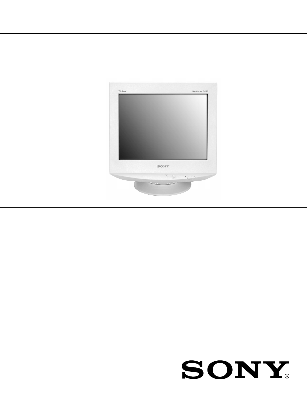
Page 1
REVISED
17VC
OPERATION MANUAL
TROUBLESHOOTING MANUAL
CHASSIS
TABLE OF CONTENTS
CIRCUIT DESCRIPTION
D Board (Power Supply Section) ............... 2
D Board (Deflection Section) .................... 11
A Board ................................................... 21
U Board ................................................... 24
GENERAL TROUBLESHOOTING ................ 26
PARTS LEVEL BOARD REPAIR ................. 37
TRINITRON® COLOR COMPUTER DISPLAY
9-978-878-02
- 1 -
Page 2
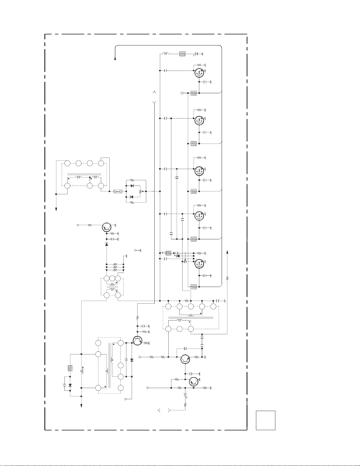
CIRCUIT DESCRIPTION
f
f
A
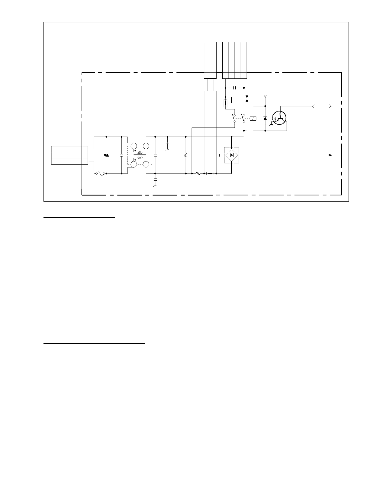
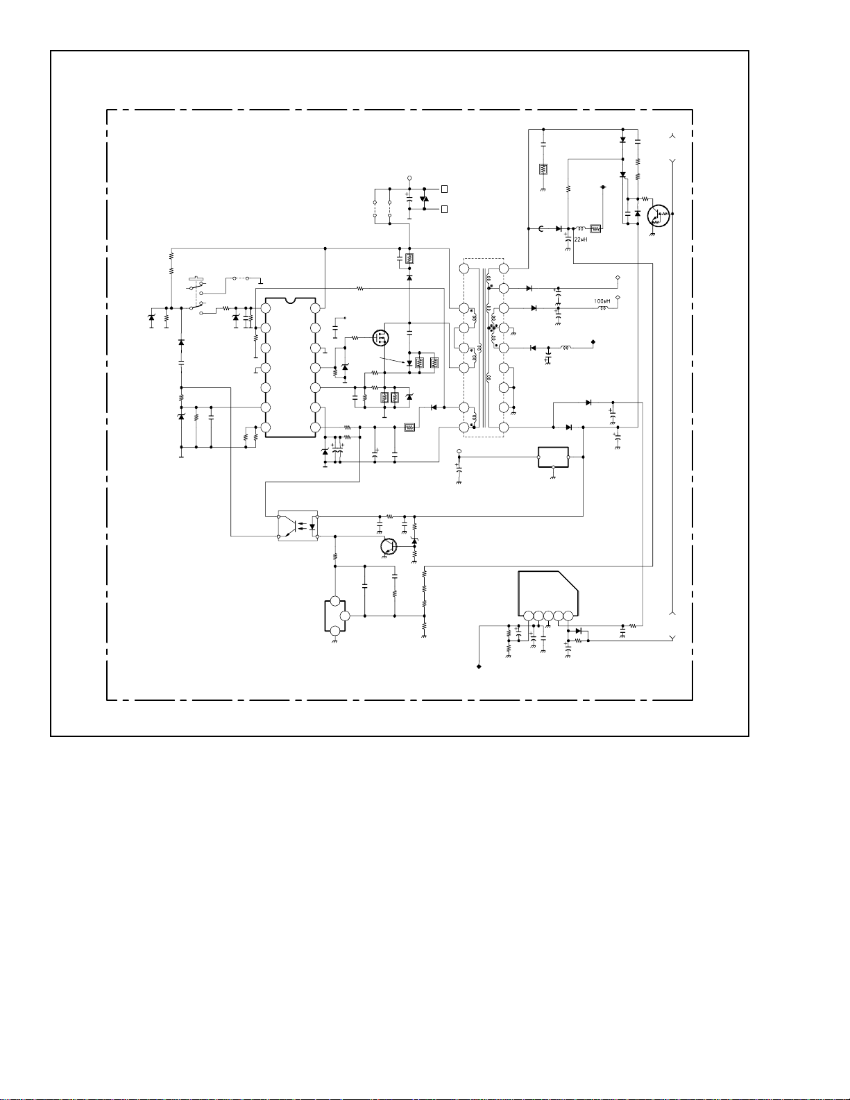
D BOARD POWER SUPPLY SECTION
Power Supply Electrical Circuit
The power supply is located on the D Board. It has three modes of operation that are controlled by a microprocessor. The
topology is a discontinuous mode flyback converter with photocoupler feedback for regulating the secondary voltages.
Circuit operation and troubleshooting are explained in the following sections:
Operation Modes Secondary Circuitry
AC Input Protection Circuits
Degauss Circuit Troubleshooting
Primary Circuitry USB/Audio Power Circuit
Operation Modes
The power supply has four modes of operation, off , active off, suspend/standby and active on. These modes are
related to power savings and are indicated by the front panel LED. Additional indications are failure diagnostics and aging
mode. The table below lists operation mode, condition and LED status.
Mode Syncs Condition LED
Off N/A Power Switch Off Off
Active Off No H and/or V Low Power, Heater Off Amber
Active On H and V Present Phase Locked, Normal Operation Green
Failure 1 N/A HV Failure Amber 0.5s<-->Off 0.5s
Failure 2 N/A H Stop, V Stop, S Cap Failure Amber 1.5s<-->Off 0.5s
Failure 3 N/A ABL Failure Amber 0.5s<-->Off 1.5s
Aging/Self Test No H and V Aging Raster or Test Pattern Amber 0.5s<-->Off 0.5s
Green 0.5s<-->Off 0.5s
Amber 0.5s<-->Off 0.5s
Except for power switch off, all modes of operation are controlled by the microprocessor located on the D Board. The
failure modes are detected by the microprocessor and the power supply is forced into active off mode. These functions
are discussed later (Deflection).
With the AC cord attached to the monitor and connected to an AC source, the monitor will be off until the power switch is
turned on. When the power switch is turned on, the power supply starts and is in active off mode. The next step is active
on mode. The active off power saving mode is activated by the microprocessor based upon the absence of either H or V
sync. If H and/or V sync signals are not present, the power supply is set to active off mode.
Power supply operation control signals are "Remote Sw", "Power Sw" and "PFC Sw". During active off mode, Remote Sw
and Power Sw are digital low and PFC Sw is digital high. To enter active on mode, the microprocessor sets PFC Sw to
digital low, then 300mS later, Remote Sw and Power Sw are set to digital high.
Output Of
180V (B+) 0V +13V +179V
80V 0V +6V +79V
+15V 0V +1V +15V
-15V 0V -1V -15V
+12V 0V 0V +12V
5V 0V 0V +5V
Heater 0V 0V +6.3V
STBY 5V 0V +5V +5V
Active Of
ctive On
- 2 -
Page 3
AC Input and Degauss
THP600A
THP600
2
0
6
N
C
P
2
DGC1
DGC2
1
0
6
N
C
NC
NC
P
4
1
2
1
0
6
H
T
5
.
4
S
M
R
V
0
2
2
S
O
P
:
2
0
6
F
N
C
0
0
6
P
3
N
1
V
C
N
2
L
3
C
A
6
0
6
1
.
0
2
5
6
F
0
1
5
A
2
5
V
0
L
L
:
T
F
1
2
4
0
7
4
0
V
3
4
6
C
4
3
7
4
0
p
0
2
5
V
0
0
6
6
C
p
0
4
0
7
2
5
0
V
6
R
0
6
C
0
0
2
.
7
2
5
4
5
6
0
k
8
2
/
1
2
W
V
R
:
C
6
0
0
R
T
H
1
3
1
0
W
3
.
4
R
6
Y
0
6
0
.
9
8
4
A
1
2
3
1
3
6
C
2
1
V
1
0
6
G
S
S
E
U
D
G
A
S
1
0
6
1
0
6
2
D
0
T
S
1
-
5
S
D
1
9
2
1
6
D
1
0
0
6
B
S
4
D
L
.
T
C
E
R
C
A
Q
S
E
P
3
4
T
1
-
C
A
T
D
R
D
Y
.
V
A
L
E
R
1. AC Input Section
The AC input section provides EMI filtering, input protection, surge limiting and CRT degauss operation.
EMI Filter
The EMI filter comprises CN600 (inlet with filter), X-capacitors C604 and C605, Y-capacitors C660 and C643 and the
line filter transformer, LF602. Input protection is provided by F601and VA601; surge current limiting by thermistor
TH600 and resistor R600. Degauss is explained in the next section.
Degauss Circuit
The degauss circuit is used to demagnetize the CRT. After power on, the microprocessor located on the D Board sets the
degauss signal to digital high and Q601 turns on relay RY601. This allows AC current into the degaussing coil through
posistor TH601. The current heats up the posistor and the resistance increases, this dampens the current in the degauss
coil to nearly zero. Duration time is approximately 5-6 seconds and the microprocessor then shuts off RY601, which
disconnects the degauss coil from the AC line. This operation should sufficiently demagnetize the CRT.
2. Primary Circuitry Section
IC601
The heart of the primary section is the TEA1504/N2 power supply controller, IC601. The following describes the functions
of each pin.
Pin 1 Vin: This is a MOSFET drain connection internal to IC601, which is connected directly to the DC mains voltage rail.
The startup current source derives power from the DC mains via the Vin pin. It supplies current to charge the Vaux (IC
supply) capacitors C616, C617 and C681 and also provides current to the IC601 control circuitry.
Pin 2 HVS: High voltage safety spacer pin is a no connection.
Pin 3 NC: Connected to primary side DC mains return.
Pin 4 Driver: Outputs the pulse width modulated gate drive for switching transistor Q602. Maximum duty cycle is set
internally at 80%.
- 3 -
Page 4

Pin 5 Isense: Provides cycle by cycle over current protection by turning off pin 4 driver output when Q602 current
exceeds the current limit corresponding to 500mV at pin 5. This pin typically provides 425nS of leading edge blanking time.
The threshold voltage for switch over to low frequency (low power) operation is sensed by pin 5. When the voltage sensed
at pin 5 is below 165mV, IC601 transitions from operating at high frequency (56.5KHz) to low frequency (23.5KHz).
Pin 6 Vaux: IC601 supply pin. An internal current source from IC601 charges the Vaux capacitors C616, C617 and C681
for startup. Once the Vaux capacitors are charged to the startup voltage level (11V), then IC601 starts switching pin 4 driver
output. The Vaux is also supplied by an auxiliary winding from T601 on the primary side once the secondary output voltages
attain their nominal operating voltage values. Pin 6 also provides under voltage lockout detection (8V) and over voltage
protection (14.7V).
Pin 7 DS: Provides the power supply for the driver output (pin 4).
Pin 8 Iref: Controls IC601 internal bias currents, which determines the pulse width modulated switching frequencies.
High frequency is 56.5KHz during active on mode. Low frequency is 23.5KHz during suspend/standby mode.
Pin 9 Vctrl: Feedback voltage for duty cycle control.
Pin 10 NC: No connection.
Pin 11 Gnd: Connected to primary side DC mains return.
Pin 12 NC: No connection.
Pin 13 Dem: Guarantees discontinuous conduction mode operation for the power supply. Verifies that T601 is demagne-
tized by not activating the next gate drive pulse until the primary side auxiliary winding of T601 is lower than the threshold
level of 65mV as detected at pin 13.
Pin 14 OOB: On/Off/Burst mode input signal. A voltage greater than 2.5V enables IC601.
Operation
The power supply is a discontinuous-mode flyback converter with photocoupler feedback for regulating the secondary
voltages. The PWM controls the pulse width of the gate drive.
When AC is applied to the power supply and IC601 pin 14 is greater than 2.5V, start up current is supplied though IC601 pin
1 to IC601 pin 6. Startup voltage is approximately 11V. After start up, the voltage to pin 6 and pin 7 of IC601 is supplied
through D620 connected to T601 pin 1. The first mode of operation is active off mode. The output drive pulse frequency
will be in burst mode operation.
When the power supply enters active on mode, the switching frequency will be 56.5KHz. The Vaux level will be approximately 12.3 volts. OVP threshold is 14.7 volts and UVLO is 8.0 volts. Therefore, if the Vaux voltage is not correct, the
power supply will not operate properly.
Feedback from the secondary side comes through IC603 and IC604, which is connected to IC601 pin 9. (See diagram on
page 5.)
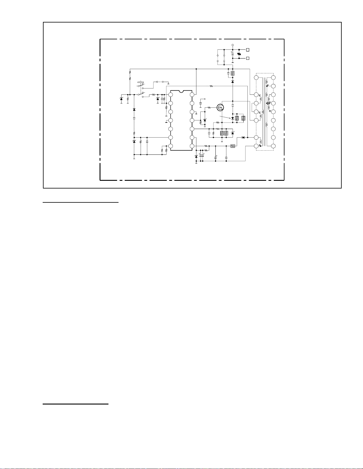
3. Secondary Circuitry Section
The secondary section consists of the following circuits: Rectifier diodes and filters for all output voltages, +5/12 volt
regulators, +5 standby regulator, heater voltage regulator, voltage feedback circuit, active off mode feedback, and protection circuits. This section will describe each circuit and its function.
Secondary Rectifiers
The secondary rectifiers supply the following voltages: 180V (B+) for deflection and video, 80V for video, ±15V for
deflection and regulators, 6.3V for heater regulator, and +5V standby regulator.
- 4 -
Page 5
2
0
C
6
0
p
1
0
0
V
5
0
6
7
p
4
k
V
2
7
6
6
R
0
1
3
5
-
1
V
5
5
6
0
R
)
.
5
7
W
(
J
1
C
6
0
3
3
1
3
6
J
W
0
4
0
)
5
7
.
W
(
J
3
6
1
R
M
.
7
4
W
/
2
1
2
0
R
6
S
M
7
4
.
W
2
1
/
2
1
5
6
R
0
k
8
6
I
P
H
:
C
5
-
D
Z
U
2
3
6
D
B
2
1
7
-
7
T
-
-
Z
J
T
M
1
1
S
S
1
6
5
C
6
0
P
I
C
H
:
8
6
1
R
6
1
R
0
2
2
k
1
P
-
C
R
N
:
C
-
N
R
:
1
D
6
7
-
7
-
-
T
J
T
Z
M
1
9
R
0
J
0
2
6
D
E
-
T
D
6
-
9
0
P
0
.
4
P
I
0
C
H
:
1
4
6
1
C
1
.
0
0
9
3
6
R
I
P
H
C
4
:
B
7
0
4
5
2
6
B
3
1
7
-
1
6
6
1
R
M
.
0
1
9
0
P
H
I
C
:
D
5
T
2
8
6
9
R
k
5
6
P
H
I
C
:
5
6
1
C
2
0
2
.
0
P
H
I
C
:
6
6
0
R
k
7
0
4
B
7
P
-
C
R
N
:
1
0
6
I
C
2
N
4
-
0
1
5
A
E
T
.
G
E
R
W
S
L
O
R
N
T
O
C
4
O
B
O
1
3
M
E
D
1
2
N
C
1
1
R
D
D
N
G
1
0
I
S
N
C
1
V
T
C
R
L
9
E
R
F
I
8
0
6
2
R
k
3
3
P
-
C
N
R
:
J
-
Z
M
T
I
6
L
P
T
O
C
T
O
P
H
C
C
C
R
4
3
E
4
7
6
C
0
p
7
4
0
V
0
5
B
N
I
V
H
E
V
I
N
E
S
A
V
3
6
D
7
-
T
0
6
C
1
D
2
U
P
O
T
N
O
I
4
A
S
O
R
R
O
T
1
H
E
S
V
2
C
N
3
R
4
3
6
0
R
k
.
8
1
C
R
:
E
5
5
0
6
C
0
0
6
8
I
H
:
C
X
U
6
5
6
5
R
0
1
0
D
S
7
8
1
8
-
7
1
6
8
C
7
4
.
V
5
0
3
-
Y
4
E
R
L
L
R
O
1
2
2
6
4
R
0
3
9
P
-
C
R
N
:
3
4
6
0
C
N
A
L
3
1
P
A
M
R
2
1
2
6
C
6
8
0
0
.
0
V
5
2
1
2
R
6
5
k
7
P
I
C
H
:
2
0
Q
6
4
3
8
K
2
S
2
2
6
0
Q
K
I
T
N
A
S
G
.
E
R
W
S
T
U
O
2
1
R
6
2
2
W
4
1
/
4
U
F
D
Z
M
T
p
P
R
6
N
:
R
1
6
6
C
2
2
V
5
2
C
S
2
1
1
6
C
0
p
8
6
I
C
H
:
1
1
C
6
0
2
7
k
2
S
7
6
0
D
2
3
G
0
7
0
7
6
5
R
8
0
6
8
-
1
J
2
3
6
R
3
3
J
Z
T
M
4
6
5
R
4
4
2
1
R
6
9
.
3
0
7
4
0
.
2
2
1
W
1
W
P
-
C
S
R
:
S
R
:
2
6
2
R
2
2
I
P
H
:
C
7
6
1
C
C
2
2
V
2
5
1
7
R
6
0
0
1
P
I
C
H
:
:
3
3
6
C
.
1
0
I
P
H
:
C
4
0
6
Q
1
A
1
3
3
T
R
O
P
3
4
C
6
p
0
7
0
4
P
I
C
H
:
4
3
R
6
P
k
2
8
P
C
N
-
R
:
A
A
0
V
B
B
3
0
A
6
V
0
1
T
6
R
T
S
E
W
5
6
3
R
k
2
2
W
3
S
:
R
6
6
0
D
2
3
G
7
0
0
4
U
F
3
p
1
9
6
R
5
6
6
R
V
5
k
.
1
5
k
.
1
W
2
2
W
S
:
R
R
S
:
6
6
1
D
B
7
.
-
4
7
-
7
T
-
2
D
6
D
1
0
P
G
R
0
4
R
6
1
D
P
R
:
F
8
6
1
1
0
.
T
:
P
5
6
C
6
.
1
0
5
V
2
P
I
C
H
1
1
R
6
2
2
I
P
C
H
:
D
6
-
7
T
J
-
Z
T
M
7
4
R
6
0
k
1
8
0
6
R
k
5
0
1
N
:
R
5
0
R
6
0
k
1
2
N
:
R
4
8
6
R
6
k
.
5
C
P
N
-
R
:
0
9
6
R
9
k
.
3
P
-
C
N
:
R
N
0
9
1
1
1
7
1
2
3
6
1
5
1
5
6
4
1
7
1
8
1
1
0
3
G
2
Y
B
T
S
0
8
C
6
2
0
2
5
0
B
2
-
1
7
4
1
2
V
5
1
4
C
6
0
0
1
V
6
1
8
6
2
R
k
.
1
9
P
-
C
N
:
R
9
6
4
R
k
.
2
2
P
-
C
R
N
:
V
3
.
6
R
T
E
A
T
H
O
E
0
W
3
1
6
1
D
A
6
U
2
-
M
C
F
0
1
6
F
B
2
1
C
6
4
7
0
V
2
5
C
7
6
1
D
R
6
1
0
G
P
1
1
8
6
D
2
S
1
-
G
N
F
M
2
3
C
6
0
0
1
0
V
5
2
2
2
D
6
S
2
G
1
-
M
N
F
6
0
C
0
0
1
2
5
D
1
0
7
6
I
C
5
T
0
B
A
G
E
R
V
5
O
G
1
J
D
D
T
A
N
U
V
G
O
0
3
C
6
0
.
1
V
0
1
7
3
C
6
6
0
C
0
2
2
7
4
V
6
1
V
1
0
G
0
7
0
4
U
F
D
T
B
5
6
2
R
8
1
0
k
.
2
2
W
/
2
1
7
6
2
R
7
.
4
0
W
/
2
1
2
6
0
L
S
S
1
2
6
2
0
0
1
V
0
0
6
0
L
V
5
1
-
0
6
L
6
0
0
1
3
0
V
1
9
6
D
2
S
1
-
G
N
M
F
4
6
1
D
A
2
T
-
S
6
N
.
3
I
2
0
6
I
C
V
T
-
S
0
A
0
A
B
G
E
R
R
E
A
T
E
H
C
L
C
T
V
C
3
6
0
D
12345
-
2
9
1
S
1
S
1
0
7
R
6
1
2
k
2
I
P
C
H
:
2
6
1
D
6
3
C
B
2
3
1
3
6
9
G
4
1
V
9
6
1
C
2
0
2
.
0
0
P
H
I
:
C
B
1
6
2
D
D
5
T
2
9
-
1
1
V
0
8
V
5
1
4
2
5
C
6
0
0
2
2
5
V
2
2
C
6
0
3
3
6
1
5
.
R
1
T
D
5
:
8
2
6
C
4
7
.
0
5
V
2
I
P
H
:
C
F
W
S
6
6
3
R
R
W
k
7
4
P
W
1
0
6
R
6
k
7
4
W
1
6
6
2
R
k
.
2
2
I
P
H
:
C
3
6
0
Q
K
A
E
1
4
1
C
D
T
R
T
E
A
H
E
W
S
4
0
V
7
9
6
2
.
W
1
S
R
W
S
R
W
P
+5/12 Volt Regulator
IC605 is the +12V regulator and IC608 is the +5V regulator. The output voltages are supplied to the microprocessor,
deflection and video circuits. The +15V line provides the input voltage for +12V regulator; the +12V line provides the input
voltage for +5V regulator. During active off mode, the +12V regulator is disabled via Remote Sw and subsequently the 5V
regulator is disabled.
+5V Standby Circuit
IC607 is the standby 5V regulator. In the active on mode the input to the regulator is supplied from T601 winding 14-13.
During the active off mode, the regulator input is supplied from T601 winding 10-13 via D612 and D613. Typical input
voltages to the regulator are active on mode: 9.5V; active off mode: 11.5V.
Heater Voltage Regulator
Heater filament voltage is supplied by T601 winding 14-13 and is regulated by IC602 to 6.3V during active on mode. IC602
output is turned on and off by the Power Sw control line at pin 1, CTL. The output is off during active off mode.
Feedback Circuit
The feedback circuit is divided into two sections. One is for active on mode; the other for active off mode. The following two sections explains the theory and operation.
Active On Mode Feedback
Shunt regulator IC604 regulates the B+ line to 179.2V by sinking current through the opto coupler 1C603 to ground. The
- 5 -
Page 6
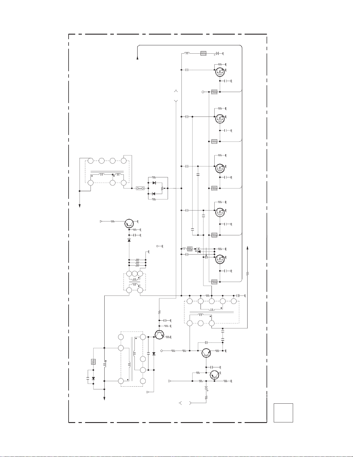
Feedback Circuits
2
0
C
6
0
p
1
0
0
V
5
0
6
7
p
4
k
V
2
7
6
6
R
0
1
3
5
-
1
V
5
5
6
0
R
)
.
5
7
W
(
J
1
0
C
6
0
3
3
1
3
6
J
W
W
(
J
3
6
1
R
M
.
7
4
W
/
2
1
2
0
R
6
6
S
M
7
4
.
W
2
1
/
2
1
5
6
R
0
k
8
6
I
P
H
:
C
5
T
-
D
Z
2
6
D
7
7
T
-
-
Z
J
T
M
U
3
B
2
1
-
D
1
1
S
S
1
6
5
C
6
0
P
I
C
H
:
8
6
1
R
0
6
1
R
0
2
2
k
1
P
-
C
R
N
:
C
-
N
R
:
0
1
D
6
7
-
7
-
-
T
J
T
Z
M
1
9
R
0
J
0
2
D
E
-
0
6
-
9
P
.
4
P
I
0
C
H
:
1
4
6
1
C
1
.
0
0
9
3
6
R
I
P
H
C
4
:
B
7
0
4
5
2
6
B
3
1
7
-
1
6
6
1
R
M
.
0
1
9
P
H
I
C
:
D
5
T
2
8
6
9
R
k
5
6
P
H
I
C
:
5
6
1
C
2
0
2
.
0
P
H
I
C
:
6
6
0
R
k
7
0
4
B
7
P
-
C
R
N
:
1
0
6
I
C
2
N
4
-
0
1
5
A
E
T
.
G
E
R
W
S
L
O
R
N
T
O
C
4
N
I
V
OOB
1
3
HVS
M
E
D
1
2
C
N
N
C
1
1
E
R
RIV
D
D
N
G
1
0
E
ENS
I
S
N
C
1
X
A
U
V
VCT
R
L
9
D
S
REF
I
8
0
6
2
R
k
3
3
8
3
6
D
P
-
C
N
R
:
1
8
-
7
7
-
T
J
-
Z
M
T
0
3
6
C
I
-
Y
4
1
D
2
6
L
P
T
E
R
L
U
P
O
O
C
T
O
P
H
L
R
O
T
N
C
O
C
C
R
4
3
4
6
0
C
I
A
L
3
1
4
A
S
A
M
O
R
R
R
E
R
7
C
:
4
7
6
C
0
p
7
4
0
V
0
5
B
6
O Q
T
1
I
ATS
H
E
2
1
R
6
2
2
2
W
4
1
/
3
4
U
F
D
Z
M
T
4
3
6
0
R
k
.
8
1
C
R
:
5
5
0
6
C
0
p
0
6
8
I
P
H
:
C
6
R
6
5
6
5
R
N
:
R
0
1
0
7
1
6
6
C
2
2
V
5
2
1
6
8
C
7
4
.
V
5
0
1
2
C
S
2
2
6
4
R
0
3
9
P
-
C
R
N
:
1
1
6
C
0
p
8
6
I
C
H
:
3
N
1
P
2
0
V
4
0
)
5
7
.
1
2
6
C
6
8
0
0
.
0
V
5
2
1
2
6
5
k
P
I
H
2
0
Q
6
4
3
8
K
2
S
2
2
0
K
N
G
.
E
R
W
S
T
U
O
1
C
6
0
2
7
V
k
2
S
7
6
0
D
2
3
G
0
7
0
7
6
5
R
8
0
6
8
-
1
J
2
3
6
R
3
3
J
-
Z
T
M
4
6
5
R
4
4
2
1
R
6
9
.
3
0
2
2
7
4
0
.
1
W
P
-
C
1
W
S
R
:
S
R
:
2
6
2
R
2
2
I
P
H
:
C
7
6
1
C
2
6
2
C
0
V
2
5
:
C
1
7
R
6
0
0
1
P
I
C
H
:
:
3
3
6
C
.
1
0
I
P
H
:
C
4
0
6
Q
1
A
1
3
3
T
R
O
P
3
4
C
6
p
0
7
0
4
P
I
C
H
:
4
3
R
6
P
k
2
8
P
C
N
-
R
:
A
A
B
B
3
0
A
6
V
0
1
T
6
R
T
S
E
W
5
6
3
R
k
2
2
W
3
S
:
R
6
6
0
D
2
3
G
7
0
0
4
U
F
3
p
1
9
6
R
5
6
6
R
5
k
.
1
5
k
.
1
W
2
2
W
S
:
R
R
S
:
6
6
1
D
B
7
.
-
4
7
-
7
T
0
2
D
6
G
D
1
0
P
G
R
0
4
R
6
1
D
P
R
:
F
8
1
1
.
T
P
C
5
6
6
.
1
0
5
V
2
P
I
C
H
1
1
R
6
2
2
I
P
C
H
:
D
6
-
7
T
J
-
Z
T
M
7
4
R
6
0
k
1
8
0
6
R
k
5
0
1
N
:
R
5
0
R
6
0
k
1
2
N
:
R
4
8
6
R
6
k
.
5
C
P
N
-
R
:
0
9
6
R
9
k
.
3
P
-
C
N
:
R
N
0
9
1
1
1
7
1
2
3
6
1
5
1
5
6
4
1
7
1
8
1
1
3
2
Y
B
T
S
0
8
6
2
0
2
5
0
B
2
-
1
7
4
1
2
V
5
1
4
C
6
0
0
1
V
6
1
8
6
2
R
k
.
1
9
P
-
C
N
:
R
9
6
4
R
k
.
2
2
P
-
C
R
N
:
V
3
.
6
R
T
E
A
T
H
O
E
0
W
3
1
6
1
D
A
6
U
2
-
M
C
F
0
1
6
F
B
2
1
C
6
4
7
0
V
2
5
C
7
6
1
D
R
6
1
0
G
P
1
1
8
6
D
2
S
1
-
G
N
F
M
2
3
C
6
0
0
1
0
V
5
2
L
2
2
D
6
S
2
G
1
-
M
N
F
6
0
C
0
0
1
2
5
D
1
0
7
6
I
C
5
T
0
B
A
G
E
R
V
5
O
G
1
J
D
D
T
A
N
U
V
G
O
0
3
C
6
0
.
1
V
0
1
7
3
C
6
6
0
C
0
2
2
7
4
V
6
1
V
1
0
G
0
7
0
4
U
F
D
T
B
5
6
2
R
8
1
0
k
.
2
2
W
/
2
1
7
6
2
R
7
.
4
0
W
/
2
1
2
6
0
L
S
S
1
2
6
2
0
0
1
V
0
0
6
0
L
V
5
1
-
0
6
6
0
0
1
3
0
V
1
9
6
D
2
S
1
-
G
N
M
F
4
6
1
D
A
2
T
-
S
6
N
.
3
I
2
0
6
I
C
V
T
-
S
0
A
0
A
B
G
E
R
R
E
A
T
E
H
C
L
C
T
V
C
3
6
0
D
12345
-
2
9
1
S
1
S
1
0
7
R
6
1
2
k
2
I
P
C
H
:
2
6
1
D
6
3
C
B
2
3
1
3
6
9
G
4
1
V
9
6
1
C
2
0
2
.
0
0
P
H
I
:
C
B
1
6
2
D
D
5
T
2
9
-
1
1
V
0
8
V
5
1
4
2
5
C
6
0
0
2
2
5
V
2
4
2
C
6
0
0
3
3
V
6
1
5
.
R
6
1
1
T
D
5
:
8
2
6
C
4
7
.
0
5
V
2
I
P
H
:
C
F
W
S
6
6
3
R
R
W
k
7
4
P
W
1
0
6
R
6
k
7
4
W
1
6
6
2
R
k
.
2
2
I
P
H
:
C
3
6
0
Q
K
A
E
1
4
1
C
D
T
R
T
E
A
H
E
W
S
7
9
2
.
W
S
R
W
S
R
W
P
reference voltage at IC604 pin 1 determines the sink current into pin 3. The reference voltage is set to 2.5 volts by
resistor divider R608, R650, R648, and R609. Since the B+ is connected to the resistor divider, any change in B+ voltage
is detected at the reference terminal. The shunt regulator will either increase or decrease the current into pin 3 in order
to decrease or increase the B+ voltage respectively and try to maintain the reference voltage to 2.50 volts. IC603 biases
it's phototransistor accordingly and drives IC601 pin 9 (Vctrl) which changes the duty cycle at IC601 pin 4 (driver) to
regulate the B+ voltage at 179.2V.
Active Off Mode Feedback
Power Sw control line is low (heater off) during active off mode and respectively Q603 is off. Voltage pulses from T601 pin
10 flow through C620, R636, and R660 triggering the gate of thyristor D613. D613 turns on effectively shorting the B+ rail
to the standby 5V regulator input; current flows from T601 pin 10 through D612 and D613 to the standby 5V regulator input.
When the standby 5V regulator input is increased to approximately 12.7V it forward biases zener diode D605 turning on
Q604 and sinks current through IC603 to ground. The standby 5V input supplies this current to IC603 pin 1. IC603 biases it's
phototransistor and drives current through D609 into IC601 pin 14 (OOB) triggering burst mode operation. IC601 pin 4
(driver) is pulled low turning off switching transistor Q602. T601 pin 1 (auxiliary winding) feedback pulses are discontinued and IC601 pin 6 (Vaux) decreases to 8V. IC601 internal current source then charges pin 6 (Vaux) to the startup voltage
level (11V) which starts switching pin 4 driver output. The feedback cycle is then repeated. The burst repetition rate is
approximately every 110mS and when IC601 pin 4 is switching its frequency is 23.5KHz.
- 6 -
Page 7
J
Z
M
T
4. Protection Circuits
Protection Circuits
-
V
5
5
3
1
5
0
6
R
)
5
.
7
(
W
J
0
1
6
C
0
3
3
3
1
6
W
J
7
(
W
J
3
1
6
R
M
7
.
4
W
2
/
1
2
0
6
R
4
1
6
R
8
6
C
:
3
6
2
D
B
1
2
-
7
7
-
T
-
0
6
S
M
7
.
W
2
/
2
5
1
k
0
P
I
H
5
T
E
-
D
Z
U
6
D
9
1
S
1
S
1
5
6
6
C
0
P
I
H
C
:
8
1
6
R
0
1
6
R
0
2
2
k
1
P
C
-
N
R
:
P
C
-
N
R
:
0
6
1
D
4
-
7
-
7
T
-
Z
J
T
M
9
1
0
R
J
2
D
-
0
-
.
P
I
H
C
:
0
1
4
1
6
C
1
0
.
0
3
9
6
R
4
6
1
9
2
7
P
I
H
C
:
B
0
7
4
5
2
3
B
1
-
7
6
1
6
R
M
0
.
1
P
I
H
C
:
8
9
6
R
D
T
5
k
6
5
P
I
H
C
:
5
1
6
C
2
2
0
.
0
P
I
H
C
:
6
0
6
R
k
0
7
4
P
C
-
N
R
:
B
1
6
0
C
I
2
-
N
4
5
0
1
E
A
T
.
E
G
R
S
W
L
R
O
T
N
C
O
4
N
I
V
B
O
O
1
3
E
D
1
2
C
N
1
1
N
G
1
0
C
N
1
C
V
9
R
I
8
0
2
6
R
k
3
3
P
C
-
N
R
:
1
S
V
H
M
2
C
N
3
R
E
V
I
R
D
D
4
E
S
N
E
S
I
5
X
U
A
V
L
R
T
6
S
D
F
E
7
8
6
3
D
8
1
7
-
7
T
-
-
J
T
Z
M
6
R
7
H
C
:
7
4
6
C
p
0
7
4
V
0
0
5
B
0
6
Q
O
T
N
I
S
T
A
E
H
2
1
6
R
2
2
W
4
/
1
0
4
F
U
D
6
Z
J
T
M
3
0
6
R
k
8
.
1
C
R
:
0
5
6
C
p
0
0
8
6
P
I
H
C
:
2
6
R
5
5
6
R
2
-
N
R
:
0
0
1
6
R
2
H
C
:
6
1
6
C
2
2
V
5
2
1
8
6
C
7
.
4
V
0
5
V
0
0
4
)
5
.
2
1
6
C
8
6
0
.
0
V
0
5
2
1
2
k
5
P
I
2
0
Q
6
3
4
2
8
K
2
S
2
K
.
G
R
E
S
W
T
O
U
1
6
C
0
7
2
k
2
S
7
0
D
6
3
G
2
7
0
7
5
6
R
8
0
1
8
-
3
2
6
R
3
3
-
J
T
Z
M
4
5
6
R
4
4
1
6
R
9
3
.
0
7
4
.
0
2
W
1
W
1
P
C
S
R
:
S
R
:
2
2
2
P
I
7
1
6
C
2
2
6
C
V
5
2
0
:
ABA
B
3
0
6
A
V
5
3
6
R
k
2
2
W
3
S
R
:
0
6
6
D
3
G
2
7
0
0
4
F
U
3
p
9
1
6
R
6
5
6
R
V
k
5
.
1
k
5
.
1
W
2
W
2
S
R
:
S
R
:
1
6
6
D
B
.
7
4
7
-
7
-
T
2
0
6
D
3
2
D
G
0
P
1
G
R
0
4
6
R
1
D
R
P
F
:
8
1
1
.
T
P
1
0
6
T
T
R
S
W
E
N
9
7
6
5
4
1
2
0
1
1
1
2
1
3
1
5
1
6
1
7
1
8
1
4
1
The following are protection circuits: OCP, OVP, UVLO and secondary short circuits. OCP is pulse by pulse and is performed
on the primary side. OVP detects excessive output voltages. UVLO detects output under voltages. The following will explain
the operation of these functions.
OCP
OCP is activated if there is too much current passing through the switching power MOSFET, Q602. This condition will
occur if either the B+ line or 80 volt line is shorted.
R614 and R654 are the current sense resistors. Current through these resistors will produce a positive voltage. R623,
R624, R657 and C650 provide a voltage divider and filter to IC601 pin 5 (Isense). If the voltage level exceeds 0.5 volts, the
IC does pulse by pulse current limit and the output voltages are reduced. This condition can be audible and characterized by
a chirping sound.
OVP and UVLO
The OVP and UVLO functions are detected by IC601 pin 6 (Vaux). Vaux is typically 12.3V. In the event the regulation control
loop were to fail, the output voltages would either increase or decrease; then Vaux would increase or decrease respectively
via T601 transformer coupling. IC601 pin 6 will detect an OVP at 14.7V and UVLO at 8V turning off the driver output and
initiating a low dissipation safe-restart mode.
Secondary Short Circuits
Safe operation during secondary short circuits is provided by the demag function of IC601 pin 13. Demag protection
reduces the switching frequency, thereby reducing the input power level and providing safe operation. Demag also
provides a soft start function during startup gradually increasing the switching frequency until fixed frequency operation
is attained.
5. Troubleshooting
Warning
Before attempting to fix the power supply, safety should be considered first. Never connect test probes to the primary side
circuits, unless proper isolation has been installed. If isolation for the AC mains is not present, serious harm can occur.
Never assume you are safe.
- 7 -
Page 8

Caution: C610 has a Slow Voltage Discharge
If the front panel power on/off button is switched to the off position prior to the AC mains input power being removed from
the monitor, then electrolytic capacitor C610 discharges with a long time constant. When the monitor cabinet cover and/or
EMI shield are removed, making the D board circuitry accessible during servicing or repair by qualified personnel, the
following procedure is recommended: Always remove the AC mains input power from the monitor prior to switching the
front panel on/off button to the off position. The AC mains input power should be removed from the monitor for a minimum of 30 seconds before the front panel on/off button is switched to the off position.
Caution: Do NOT Touch IC610 Component Tab or Heat Sink
IC610 component tab has an electrical voltage potential equivalent to the primary side return (approximately AC mains
input voltage potential). If IC610 heat sink insulator pad and/or shoulder washer busing are damaged or not assembled
correctly, then the IC610 heat sink will have an electrical voltage potential equivalent to primary side return (approximately
AC mains input voltage potential).
No Power
In the event that the monitor does not turn on, first verify input power is applied to CN600 and the front panel power button
is turned on; then check F601. If F601 is blown, the primary side circuitry should be checked. If the fuse is not blown, then
check the secondary side circuitry, especially the protection circuits. If these circuits are causing a no power symptom, the
problem can be more readily found.
AC Input and Degauss Circuit Trouble Shooting
For no power or nonoperating power supply, the AC input circuitry should be checked. Open or short circuit elements will
cause non-operation. Check F601, CN600, D601, R600, TH600 and R605 on the D Board. Check the front panel power
button for continuity.
If all elements are correct, check whether F601 breaks when power is applied and the power button is closed. If the fuse
does blow, there probably is a component shorted in the prmary circuitry.
The degauss will malfunction if CN601 is not connected. One problem could be loss of degauss signal from the microprocessor. This can be verified by using the manual degauss command found in the OSD menu. If the signal does not appear at
Q601 base, then it is possible that the microprocessor does not function correctly or standby 5V is not functioning.
The second step is to place a short across the AC terminals of RY601 for less than two seconds. If degauss operates then
check Q601 and RY601. If degauss does not work, check TH601 for an open condition and C631 for a short condition.
Primary Section
Three main areas can diagnose primary circuit failures. These are IC601, Q602 and Feedback system.
Visible checks of these areas will aid in finding problems. The following will discuss each section.
IC601
First apply AC to the monitor and check IC601 pin 4 output. If the output on pin 4 is not present, there could be problems
with Q602 and related parts or pin 14 could be less than 2.5 volts. Further, check Vaux level at pin 6. If it less than 11V,
the IC could be in safe-restart mode. If the voltage is very low, there could be a short on any of the IC pins. In reference
to ground, check the impedance of pin 1, 8 and 14. If any of these pins are shorted, replace the IC and check components
connected to the related pins. Take care that C616, C617 and C681 are fully discharged before replacing the IC.
Q602
The switching transistor can be damaged in various ways. These are related to voltage, current and temperature.
Check whether the transistor is shorted across drain and source terminals. If there is a short, F601, R605, R614, R654,
R623, R624, R657 and C650 should be checked. Additional components to check are D608, R603, R612 and IC601. If
Q602 is shorted, all these parts should be replaced.
Failure of a secondary rectifier diode can also cause Q602 to fail. Check 180V and 80V diodes for open or short
conditions. There is also a clamp circuit, which is used to clip the turn off spike found on Q602 drain. If the clamp
circuit is broken, it can cause Q602 failures. Check D606, C612 and R635. Also check the snubber circuit components
C613, D607, R619 and R656.
Secondary Circuit
Failure in the secondary circuits can be categorized by rectifier diodes, regulators, feedback loops and protection circuits.
- 8 -
Page 9

These sections are interrelated and failure in one can affect another. Consequently, some failures will also affect the
primary circuitry.
Rectifier Section
Rectifier diode failures are not common, but do occur. Deflection, video and high voltage circuitry failures contribute to
diode damage. In the event a voltage is not present, check for shorts to ground, open or short diodes.
+5/12 Volt Regulator
If +12V or +5V output line is not available or the wrong voltage, IC605 or IC608 may be damaged. Before replacing
either IC, check for shorts or damaged parts along the output lines. If +12 volt does not appear, check the Remote Sw
signal from IC901 pin 6.
Standby 5V Circuit
Failure of this circuit can be affected by IC607. In case the circuit does not work properly, check D605, D614, R611 and
Q604. If these components are good, check the remaining circuit parts. Another possible influence can be the heater
circuit. Since both the standby 5V and heater voltages are produced by T6-1 winding 13-14.
Heater Voltage Regulator
This circuit may be affected by R697 or D619. If these parts are good, check the regulator output for a short to ground.
Shorts can occur on the video board. In the case of Power Sw signal.
Feedback Circuit
Problems with feed back can cause power supply shut down and low or high output voltages. First determine whether the
power supply is operating in active off, active on modes or not at all.
The power supply can be stuck in active off mode. The Remote Sw signal, Q603, Q604, D605 and IC603 can affect this
condition. Likewise, if the power supply is always in active on mode, the same items should be checked, along with
D612, D613, D621, C619, C620, R626, R636 and R660.
Checking for voltages at IC603 pins 1 and 2, IC604 pins 1 and 3 can solve more difficult problems. Additionally, IC603
pins 3 and 4, and IC601 pin 9 should be checked. If there are problems with these devices, 180V or standby 5V line, the
feedback systems will not work correctly. Also check the protection circuits.
Protection Circuits
OCP occurs when there is excessive current through Q602. Failures with Q510, Q507 or the video section could cause
this condition. These areas should be checked. OCP condition can also occur if R614 or R654 are open; if R623 or
R657 are shorted; or if R624 is open.
OVP usually occurs when the feedback loop is open, or loss of standby 5V. Isolate the OVP trigger condition, by first
checking the operation of the feedback loop.
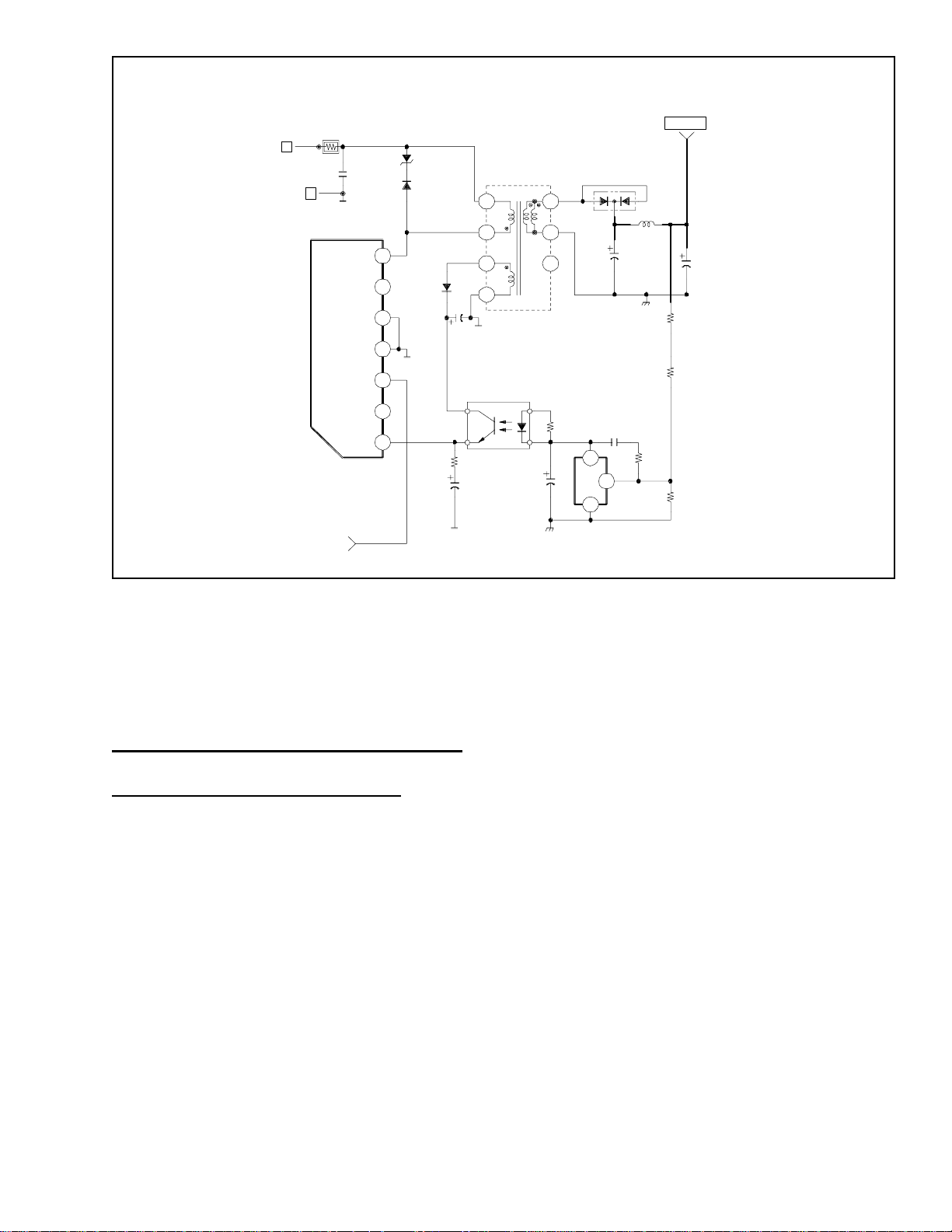
6. USB/Audio Power Circuit
CAUTION: Do not touch IC610 component tab or heat sink. The IC610 component tab has an electrical voltage
potential equivalent to the primary side return (approximately AC mains voltage potential). If the IC610 heat sink insulator
pad and/or shoulder washer bushing are damaged or not assembled correctly, then the IC610 heat sink will have an electrical
voltage potential equivalent to the primary side return (approximately AC mains voltage potential).
The USB/Audio power supply circuit is a flyback converter that uses an integrated power mosfet and switch mode pwm
control IC (IC610). The circuit consists of IC610, T602, D633, PH601, IC611 and associated circuitry. Start up is
initiated when C675, connected to the CONTROL pin 1 is charged via a high voltage current source internal to IC610.
When CONTROL pin 1 reaches 5.8V, the control circuitry and mosfet are activated and a 10mS soft-start begins. The
typical mosfet DRAIN pin 7 switching frequency is 130 KHz with a ±4KHz jitter. The feedback loop consists of shunt
regulator IC611 and optocoupler PH601 that will regulate the secondary side output voltage at 6.5V and provide feedback
current to CONTROL pin 1. During normal operation, T602 bias winding pins 3-4 provide the charging current to maintain
CONTROL pin 1 at 5.8V; additionally the CONTROL pin 1 charging current that is regulated by IC611 and PH601 controls
the mosfet duty cycle to provide closed loop regulation.
The front panel power button controls the on/off function for the USB/Audio power circuit. When the power button is in
the OFF position, the MULTIFUNCTION pin 3 is shorted to CONTROL pin 1, turning off the power circuit. When the
power button is in the ON position, the MULTIFUNCTION pin 3 is shorted to primary side DC mains return, which enables
the power circuit.
- 9 -
Page 10
2
1
S Cap Sws
H Deflection Circuit
TO:
180V
H Lin and
Ringing Circuit
12V
C575
FB506
5
R581
3
D518
Q521
T505
Q520
B+CHOP
R582
HST
3
C574
HDY-
4
HDY-
3
1
D516
L503
HOC
FB504
T504 HDT
1
H DY+
2
8
H DY+
1
1
2
6
TO: IC901 #32 pin
H FLY
Q508
D502
4
IC902 #14 pin
C521
C518
D506
R518
R517
R513
Q511
C522
Q507
H-OUT
C510
FB507
R522
R511
FB508
-15V
C543
R551
C563
20
3
R553
Out
H Reg
IN
H Def
IN
HD
PWM IC501
IN
H SHAPE
IC902
E/W PIN #9
8
2
R569
R584
R583
C582
- 10 -
C576
12V
12V
R504
R933
CN801
R509
C502
Q501
R594
Q903
HD output pin #17
IC902
R508
D501
Q502
Page 11
1
8
2
3
4
5
6
1
2
4
3
1
2
3
1
2
3
4
5
6
7
C
6
7
0
C
6
7
1
C
6
7
2
C
6
7
3
C
6
7
5
C
6
7
6
C
6
7
7
D
6
3
3
D
6
3
4
D
6
3
5
D
6
3
6
I
C
6
1
0
I
C
6
1
1
L
6
0
7
P
H
6
0
1
R
6
3
0
R
6
3
1
R
6
3
2
R
6
3
4
R
6
3
9
R
6
4
1
R
6
5
1
T
6
0
2
*
*
*
*
*
*
*
*
*
*
*
*
P
O
W
E
R
S
U
P
P
L
Y
C
O
N
T
R
O
L
I
C
*
E
R
R
O
R
A
M
P
*
*
C
O
N
T
R
O
L
*
*
*
*
*
*
*
*
S
R
T
D
F
S
M
C
A
B
+
6
.
5
V
To SW 602
USB/Audio Power Circuit
A voltage clamp to limit the peak voltage on DRAIN pin 7 is provided by D635 and D636. Bypass capacitor C677 is
utilized to improve high frequency noise immunity.
IC610 provides the following protection functions: a 10mS soft-start function, a cycle-by-cycle peak current limit function, a shutdown/auto-restart function if an out of regulation condition occurs and an over temperature protection function.
D BOARD DEFLECTION SECTION
1. Horizontal Deflection Circuit
Overview
These circuit drive the DY (Deflection Yoke) for Horizontal Deflection. The H size and H shape control (IC501 and around)
is included in this page as well.
H Drive, H Out, Feedback
+12Vp-p HD pulse is generated by the inverter Q903 using the Jungle IC902 H. out pin #17. And switch Q511 through A
push-pull amplifier (Q501 and Q502) buffers. The drive current which introduced in HDT (T504) by this switching will
drive Q507 (H out Tr) and 1000V pulse appears on collector. D506 is the "Damper Diode" which avoid the negative pulse
and discharge the energy for next Horizontal Drive. Q508 is the buffer for the "H BLK" feed back to Jungle IC 902 H. FLY
pin #14 and it will be the reference of phase / jitter control of Jungle. HST (T505) is to sense the deflection current
through DY. The voltage appeared on secondary side will be the feed back for H Size/Shape control.
H Size/Shape control
HD pulse also triggering the H Size/Shape control IC501 pin #8. IC501 is "PWM IC" and it controls H and HV B+
chopper duty. H Shape and H size information is already included and coming from Jungle IC902 E/W pin #9. It will be
supplied to IC501 pin #2. H reg output pin #20 is switching pulse of Q520 (B+ chopper). The energy supplement from
180V to H Def circuit (through L503 HOT) is controlled by the duty of this pulse. The H Shape input and feedback
voltage from T505 are compared by error amp (in IC501) and H Reg out pulse duty is controlled to keep the level of
these two the same.
- 11 -
Page 12
H
6
m
0
2
8
5
.
7
L
2
5
3
5
&
1
0
2
9
5
C
,
I
1
5
M
,
O
0
R
5
F
,
9
4
S
N
I
P
0
C
1
C
5
H
L
7
8
1
+
Y
O
D
T
H
V
2
1
5
6
6
0
U
2
7
5
0
0
4
R
2
3
L
5
N
D
1
1
0
D
3
P
k
9
I
7
8
H
.
5
C
4
R
:
1
9
5
R
5
W
T
0
E
S
5
N
H
T
5
4
S
P
U
0
1
W
K
A
1
7
2
3
5
0
Q
1
A
S
2
D
T
5
2
2
1
-
5
9
D
1
1
S
S
1
W
0
N
4
5
R
/
1
:
1
3
2
9
0
2
3
2
2
7
L
/
5
5
4
1
R
N
D
W
1
S
D
P
0
C
k
9
-
2
5
N
2
R
R
:
1
7
T
0
1
P
.
5
:
0
C
6
W
0
N
1
4
5
R
5
/
1
:
R
1
2
W
N
0
9
4
5
R
5
/
:
1
R
1
5
4
1
4
1
#
0
9
N
C
I
I
P
N
I
L
H
R
2
E
W
0
0
2
T
0
5
/
1
N
V
1
R
E
C
H
3
0
0
P
L
C
H
m
2
.
2
5
0
5
L
R
7
V
9
P
4
0
2
P
0
5
0
:
.
C
4
0
7
5
V
P
4
0
2
P
0
5
0
:
.
C
4
0
2
V
3
1
1
P
8
0
2
3
.
P
0
5
5
5
0
:
.
2
C
C
0
V
7
6
P
1
0
2
P
5
5
.
:
2
0
C
P
P
:
V
0
8
0
6
4
5
C
7
4
0
.
0
D
W
5
0
2
R
7
2
7
0
7
P
.
/
5
1
5
F
4
1
R
C
:
V
2
4
P
A
8
0
1
P
T
5
.
5
:
1
0
2
-
C
1
0
5
4
D
L
N
1
D
5
P
k
8
I
2
2
H
P
.
5
C
1
6
I
2
R
:
0
0
H
.
5
C
0
C
:
A
1
9
1
1
6
T
W
0
5
T
6
3
5
C
E
3
Q
L
N
C
S
2
5
7
7
S
0
W
7
R
0
3
5
:
1
R
p
1
V
0
8
k
0
5
1
2
C
2
8
C
W
0
L
E
5
N
H
L
U
0
5
2
0
L
5
N
D
1
D
O
T
0
1
Y
D
H
3
2
1
V
2
1
B
W
S
P
2
I
H
-
C
V
:
0
B
7
2
1
.
0
E
T
8
9
5
0
0
5
5
5
3
C
D
S
S
1
P
k
1
6
I
8
7
H
.
5
C
6
R
:
4
N
9
1
R
3
5
:
R
k
5
k
6
N
N
0
6
0
0
R
R
3
5
3
5
:
:
3
R
3
R
R
Q
P
-
M
4
A
A
0
1
5
5
4
F
k
Q
0
9
0
D
5
1
3
.
R
C
V
S
2
V
2
1
2
2
1
0
#
9
C
N
I
I
P
V.DF
2
0
5
R
V
3
2
7
0
7
k
N
.
3
5
5
W
0
S
2
R
0
/
:
1
1
V
5
Y
B
T
S
V
P
0
P
5
:
2
D
5
R
k
2
P
1
5
F
R
:
P
P
:
V
0
5
2
5
1
P
.
P
0
:
0
V
3
0
5
5
C
2
8
6
0
.
0
V
1
0
1
5
5
2
C
2
7
1
.
5
4
R
4
7
p
V
4
0
0
0
B
3
0
5
3
5
C
P
k
1
C
0
0
-
0
5
N
2
C
R
:
1
0
5
R
R
6
2
5
2
C
5
:
R
E
G
2
N
3
6
A
S
3
1
H
3
5
C
K
Q
S
P
2
A
C
D
6
R
k
3
P
1
5
F
R
:
5
k
3
6
5
5
R
D
3
R
k
3
P
1
5
F
R
:
3
k
2
6
5
5
R
4
k
2
6
5
5
R
D
1
R
k
2
P
1
5
F
R
:
5
k
1
1
5
R
3
S
P
1
8
I
0
3
H
.
5
C
0
C
:
B
0
S
N
R
:
E
G
2
N
S
3
A
5
3
H
1
3
C
5
K
Q
S
P
2
A
C
S
P
1
6
I
0
3
H
.
5
C
0
C
:
B
1
S
N
R
:
E
G
N
8
S
A
9
2
H
0
1
C
2
5
K
Q
P
S
2
A
C
P
S
1
0
I
0
2
H
.
5
C
0
C
:
B
2
S
N
R
:
E
G
S
8
N
9
3
A
0
1
H
2
5
C
K
Q
S
P
2
A
C
S
P
1
5
I
0
1
H
.
5
C
0
C
:
B
9
M
1
1
5
R
S
4
1
5
Q
P
1
2
I
0
1
H
.
5
C
0
C
:
B
D
R
7
P
0
F
5
:
C
2
5
T
3
S
1
B
#
F
N
O
I
T
P
E
G
8
N
9
A
0
H
2
C
K
S
P
2
A
C
)
S
8
5
3
1
5
(
R
W
J
4
S
8
V
1
0
.
0
0
4
1
T
3
F
0
D
5
:
T
8
1
F
V
7
p
k
5
0
2
1
C
5
V
p
0
k
0
5
1
2
C
k
7
N
7
0
R
.
5
:
P
2
R
1
3
I
0
0
H
.
5
C
0
C
:
B
7
R
3
5
E
0
0
F
1
5
F
A
Q
U
S
B
2
P
3
C
k
0
0
-
0
1
5
N
1
R
R
0
0
1
:
(BOARD)
D
H. LINEARITY AND RASTER DISTORTION CORRECTION CIRCUIT
- 12 -
Page 13
H
6
m
0
2
8
5
.
7
L
2
5
3
5
&
1
0
2
9
5
C
,
I
1
5
M
,
O
0
R
5
F
,
9
4
S
N
I
P
0
C
1
C
5
H
L
7
8
1
+
Y
O
D
T
H
V
2
1
5
6
6
0
U
2
7
5
0
0
4
R
2
3
L
5
N
D
1
1
0
D
3
P
k
9
I
7
8
H
.
5
C
4
R
:
1
9
5
R
5
W
T
0
E
S
5
N
H
T
5
4
S
P
U
0
1
K
A
1
7
2
3
5
0
Q
1
A
S
2
D
T
5
2
2
1
-
5
9
D
1
1
6
S
1
S
5
1
R
W
0
N
4
5
R
/
1
:
1
3
4
2
9
0
2
3
2
7
L
5
5
4
R
N
D
W
1
S
D
P
0
C
k
9
-
2
5
N
2
R
R
:
1
7
T
0
1
P
.
5
:
0
C
W
0
N
4
5
R
/
1
:
1
2
W
N
0
9
4
5
R
5
/
:
1
R
1
5
1
4
1
#
0
9
N
C
I
I
P
N
I
L
H
R
2
E
W
0
0
2
T
0
5
/
1
N
V
1
R
E
C
H
W
2
/
1
3
0
0
P
L
C
H
m
2
.
2
5
0
5
L
R
7
9
V
P
4
0
2
P
0
5
0
:
.
C
4
0
7
5
V
P
4
0
2
P
0
5
0
:
.
C
4
0
2
V
3
1
1
P
8
0
2
3
.
P
0
5
5
5
0
:
.
2
C
C
0
V
7
6
P
1
0
2
P
5
5
.
:
2
0
C
P
P
:
V
0
8
0
6
4
5
C
7
4
0
.
0
D
W
5
0
2
R
7
2
7
0
7
P
.
/
5
1
5
F
4
1
R
C
:
V
2
4
P
A
8
0
1
P
T
5
.
5
:
1
0
2
-
C
1
0
5
4
D
L
N
1
D
5
P
k
8
I
2
2
H
P
.
5
C
1
6
I
2
R
:
0
0
H
.
5
C
0
C
:
A
1
9
1
1
6
T
W
0
5
T
6
3
5
C
E
3
Q
L
N
C
S
2
5
7
7
S
0
W
7
R
0
3
5
:
1
R
p
1
V
0
8
k
0
5
1
2
C
2
8
C
W
0
L
E
5
N
H
L
U
0
5
2
0
L
5
N
D
1
D
O
T
0
1
Y
D
H
3
2
1
V
2
1
B
W
S
P
2
I
H
-
C
V
:
0
B
7
2
1
.
0
E
T
8
9
5
0
0
5
5
5
3
C
D
S
S
1
P
k
1
6
I
8
7
H
.
5
C
6
R
:
4
N
9
1
R
3
5
:
R
k
5
k
6
N
N
0
6
0
0
R
R
3
5
3
5
:
:
3
R
3
R
R
Q
P
-
M
4
A
A
0
1
5
5
4
F
k
Q
0
9
0
D
5
1
3
.
R
C
V
S
2
V
2
1
2
2
1
0
#
9
C
N
I
I
P
V.DF
2
0
5
R
V
3
2
7
0
7
k
N
.
3
5
5
W
0
S
2
0
R
/
1
:
1
V
5
Y
B
T
S
V
P
0
P
5
:
2
D
5
R
k
2
P
1
5
F
R
:
P
P
:
V
0
5
2
5
1
P
.
P
0
:
0
V
3
0
5
5
C
2
8
6
0
.
0
V
1
0
1
5
5
2
C
2
7
1
.
5
4
R
4
7
p
V
4
0
0
0
B
3
0
5
3
5
C
P
k
1
C
0
0
-
0
5
N
2
C
R
:
1
0
5
R
R
6
2
5
2
C
5
:
R
E
G
2
N
3
6
A
S
3
1
H
3
5
C
K
Q
S
P
2
A
C
D
6
R
k
3
P
1
5
F
R
:
5
k
3
6
5
5
R
D
3
R
k
3
P
1
5
F
R
:
3
2
5
R
4
k
2
6
5
5
R
D
1
R
k
2
P
1
5
F
R
:
5
1
5
R
3
S
P
1
8
I
0
3
H
.
5
C
0
C
:
B
0
S
N
R
:
E
G
2
N
S
3
A
5
3
H
1
3
C
5
K
Q
S
P
2
A
C
S
P
1
6
I
0
3
H
.
5
C
0
C
:
B
1
S
k
N
R
6
5
:
E
G
N
8
S
A
9
2
H
0
1
C
2
5
K
Q
P
S
2
A
C
P
S
1
0
I
0
2
H
.
5
C
0
C
:
B
2
S
N
R
:
E
G
S
8
N
9
3
A
0
1
H
2
5
C
K
Q
S
P
2
A
C
S
P
1
5
I
0
1
H
.
5
C
0
C
:
B
9
M
1
1
5
R
S
4
1
5
Q
P
1
2
I
0
1
H
.
5
C
0
C
:
B
D
R
7
k
P
0
1
F
5
:
C
2
5
T
3
S
1
B
#
F
N
O
I
T
P
E
G
8
N
9
A
0
H
2
C
K
S
P
2
A
C
)
S
8
5
3
1
5
(
R
W
J
4
S
8
V
1
0
.
0
0
4
1
T
3
F
0
D
5
:
T
8
1
F
V
7
p
k
5
0
2
1
C
5
V
p
0
k
0
5
1
2
C
k
7
N
7
0
R
.
5
:
P
2
R
1
3
I
0
0
H
.
5
C
0
C
:
B
7
R
3
5
E
0
0
F
1
5
F
A
Q
U
S
B
2
P
3
C
k
0
0
-
0
1
5
N
1
R
R
0
0
1
:
(BOARD)
D
(17VC H. CENTERING CIRCUIT)
- 13 -
Page 14

Troubleshooting
See attached FLOW CHART and confirm if its really an H Deflection issue.
No H Deflection / No Power
Check Q507, Q520 and D506 first. In case any of these shorted, check T504, Q511, R511 and D502.
Those parts might have been damaged.
If both of Q507, 520 were not broken, check the HD pulse at the gate of Q511.
If no pulse, check Q501, Q502, Q903.
Otherwise, check R582, D518 or try changing IC501.
Bad Distortion
Check pin#2 of IC501 and confirm that proper DC level and AC waveform.
If the distortion is on only right side, check all above (No H Deflection).
Otherwise, refer to the Troubleshooting of next section (H Lin and Ringing Correction).
2. H Linearity and Raster/Distortion Ringing Correction Circuit
This section includes HLC Control circuit, S cap switching and HLC/S-Cap Damping circuits. These circuits are placed
directly on the cool side of DY which is in series with deflection current line. H Centering circuit will be explained in
next section.
HLC Balance Control and HLC Damping
HLC (L508) effectiveness is changed by LCT (T506) for each fH since T506 and L508 are in parallel. LCT is the Cross
Transformer that can change its inductance accordingly to the DC current of the secondary side. The current of the
secondary side is controlled by the DAC output of Micro (IC901 - pin 4) through Q519. It can be changed by the register
"HLIN_BAL_LOFH", "HLIN_BAL_MDFH" and "HLIN_BAL_HIFH". D505, C581 and R577 make up the damping
circuit to avoid Raster Ringing (mainly on the left side of the picture) caused by HLC, DY and S-caps.
S-Cap switching and S-cap Damping
H Def current is distorted by resonance between S-Cap and DY to correct the linearity. Since the resonance frequency
has to be changed for each fH, S-Cap switching is controlled by MICRO
S-Cap Switch - FETs (Q512, Q513, Q514, Q515, Q516) are "On" when its gate is Hi(5V) and that moment, drain voltage
should be grounded (0V).
L506, R578 and C573 is damping circuit to avoid Distortion Ringing (mainly on top of the picture) caused by S-caps and
H Control loop gain. L505, R575 and C572 is also the same purpose as above but only works when Q514 (Switch for the
Biggest S-Cap) is On.
Troubleshooting
See attached FLOW CHART and confirm if its really H lin issue.
Bad Linearity
Confirm that Raster is approximately in the center of the Bezel. If not, refer to next section (Raster Centering Circuit).
Check S-cap switches (Q512, 513, 514, 515, 516, HLC switch (Q519)) and confirm that H Linearity changes proportional to the value of S-Cap DAC. Confirm that H.LIN BAL changes by the register value of "HLIN_BAL_LOFH",
"HLIN_BAL_MDFH" and "HLIN_BAL_HIFH". If not working, check Q519, C508 or T506.
Bad Top Distortion/ Left side Raster Ringing
Check damping circuits explained above.
3. H. Raster Centering Circuit
Overview
H center circuit is changed from D99 type in which the Power OP-Amp is used
H Center Circuit
H Centering is changed by rotating RV502 to change the current through HCC (L510). Micro is no longer controlled.
Troubleshooting
See attached FLOW CHART and confirm if its really H Center Circuit issue.
No Raster Centering Control
Check R526, R529 and L510 first. Then, check D530, and D531. If these parts are good, check RV502.
- 14 -
Page 15
#1, 2 PIN
Rotation Coil (CN701)
R563
R562
Rotation/Vertical Key Circuit
STBY
5V
R558
+15V
IC502
C549
5
V+
1
+
V-
-
2
3
4
R559
R560
C547
ROTATION
3
IC901
R566
-15V
C513
4. Rotation Circuit
Rotation is a PWM waveform at approximately 125kHz measuring 5Vp-p at pin #3 of the micorprocessor IC901. Then
filtered by R560 and C547 combination. The DC current is output by powered OP-amp (IC502). The output current from
pin #4 of IC502 flows through R563 and the rotation coil and returns to ground through R566. The feedback is sensed at
R566 and sent back to the amplifier through R562.
No Rotation Control
Check the waveform pin #3 of microprocessor IC901 if it is 5Vp-p PWM and approximately 125kHz. Otherwise, check
around IC502.
5. Dynamic Focus Circuit
Overview
Both H and V Dynamic Focus are combined through DFT (T503).
H DF
Horizontal Parabola is injected into the secondary side of the focus transformer (DFT:T503). In order to keep the amount
of parabola constant over the horizontal frequency range the values of the AC coupling capacitors are changed by the
transistors, which switch the s-caps. This signal is amplified by the turns-ratio to the primary side of the transformer.
V DF
V DF waveform is buffered by Q505 and amplified by Q504 to about 130Vp-p. VDF is controlled by Jungle IC902 pin #12.
300v Vcc is made by FBT through D515. This voltage is also used for HV Protector.
Troubleshooting
See attached FLOW CHART and confirm if it is really a DF issue.
Bad H DF
Check H. Linearity. If there is no problem, change T503 (DFT).
Bad V DF
Confirm that waveform is around 1Vp-p from Jungle pin 12 of IC902. If its more than 2.0Vp-p, change Jungle IC902.
Check 300v from FBT.
- 15 -
Page 16
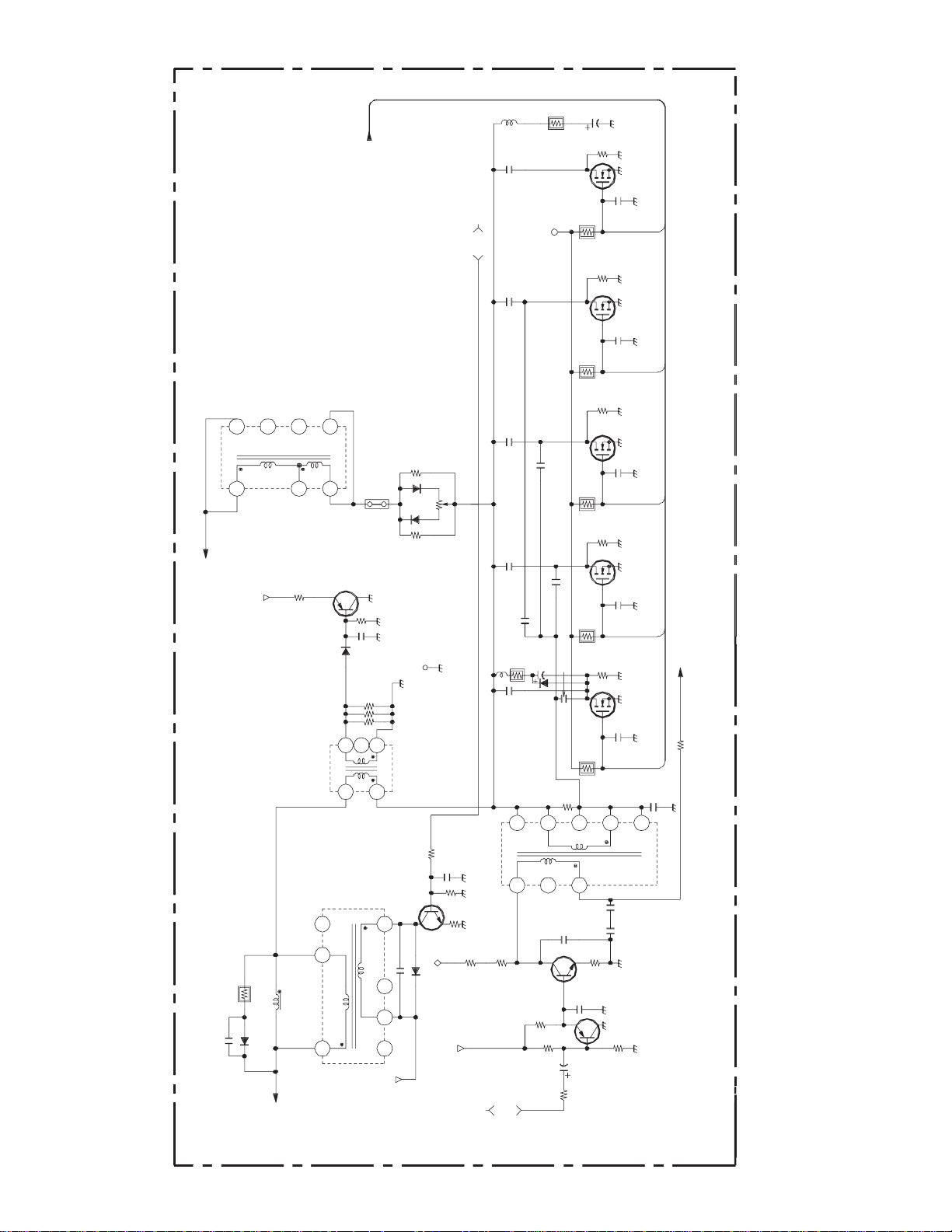
+
Y
O
D
T
H
Dynamic Focus Circuit
7
0
7
0
5
1
R
p
1
V
0
8
k
0
5
1
2
C
2
H
6
m
0
2
5
.
L
3
5
&
1
0
2
9
5
C
,
I
1
5
M
,
O
0
R
5
F
,
9
4
S
N
I
P
0
C
1
C
5
H
L
7
8
1
V
2
1
5
6
R
2
6
U
2
5
0
0
R
2
3
L
5
N
D
1
1
0
D
3
P
k
9
I
7
8
H
.
5
C
4
R
:
1
9
5
R
5
W
T
0
E
S
5
N
H
T
5
4
S
P
U
0
1
K
A
1
7
2
3
5
0
Q
1
A
S
2
D
T
5
2
2
1
-
5
9
D
1
1
6
S
1
S
5
1
R
W
0
N
4
5
R
/
1
:
1
3
4
2
9
2
3
2
L
5
5
R
N
D
W
1
S
D
P
0
C
k
9
-
2
5
N
2
R
R
:
1
7
T
0
1
P
5
.
:
0
C
W
0
N
4
5
R
/
1
:
1
2
W
0
9
4
5
5
/
1
R
1
5
1
E
W
0
0
0
2
T
7
0
5
/
1
4
N
V
1
R
E
C
H
W
0
2
7
/
4
1
3
0
0
P
L
C
N
R
:
2
7
9
V
P
4
0
2
4
P
0
5
0
1
:
.
#
C
4
0
0
9
N
C
I
I
P
N
I
L
H
7
5
V
P
4
0
2
P
0
5
0
:
.
C
4
0
V
3
1
P
0
2
.
P
5
5
0
:
2
C
V
7
6
P
1
0
2
P
5
.
5
:
2
0
C
P
P
:
V
0
8
0
6
4
5
C
7
4
0
.
0
H
m
D
5
W
0
2
R
7
2
0
.
P
5
/
1
2
F
R
1
:
5
0
5
L
V
2
4
P
8
0
1
P
5
.
5
:
0
2
C
5
P
k
8
I
2
2
H
P
.
5
C
1
6
I
2
R
:
0
0
H
.
5
C
0
C
:
A
1
9
1
W
1
6
T
W
3
0
C
E
5
L
N
T
6
7
S
W
R
3
:
8
C
W
0
L
E
5
N
H
L
U
0
5
2
0
L
5
N
D
1
D
O
T
0
1
Y
D
H
S
5
3
Q
C
S
2
5
P
I
H
C
:
B
1
.
3
0
9
0
5
C
2
1
V
2
1
B
P
k
1
6
I
7
8
H
5
.
C
6
R
:
4
N
9
1
R
3
5
:
R
k
5
k
6
N
N
0
6
0
0
R
2
5
R
V
0
7
2
E
T
8
5
0
5
5
3
D
S
S
1
V
2
1
2
1
#
N
I
P
R
3
3
5
:
:
3
3
R
R
Q
P
-
M
4
A
A
0
1
5
4
F
Q
9
D
3
.
C
V
S
2
2
0
V.DF
9
C
I
3
V
2
7
7
0
k
N
.
3
5
5
W
8
0
S
C
7
2
0
R
5
/
1
:
1
R
6
3
V
5
5
R
Y
B
T
S
3
3
5
R
2
V
1
P
8
0
3
P
0
5
5
:
.
2
C
0
D
5
R
k
2
P
1
5
F
R
:
P
P
:
V
0
5
2
5
1
P
.
P
0
:
0
V
3
0
5
5
C
2
8
6
0
.
0
1
V
2
7
1
2
0
7
.
1
5
5
5
4
5
R
2
C
C
A
T
1
-
1
0
5
4
D
L
N
1
D
2
7
1
.
5
4
R
3
4
7
8
p
V
4
0
0
0
B
3
0
5
3
5
C
5
k
0
0
5
1
R
P
k
2
1
C
0
0
0
-
0
5
5
N
2
R
C
R
:
1
0
5
R
R
6
2
5
2
5
:
R
E
G
2
N
3
6
A
S
3
1
H
3
5
C
K
Q
S
P
2
A
C
D
R
k
P
1
F
:
5
k
N
3
6
R
5
5
:
R
D
R
k
P
1
F
:
3
k
2
6
5
5
R
4
k
N
2
6
R
5
5
:
R
D
R
k
P
1
F
:
5
k
1
1
5
R
3
0
5
C
0
1
0
0
1
S
P
1
8
I
0
3
H
.
5
C
0
C
:
B
0
S
E
G
2
N
S
3
A
5
3
H
1
3
C
5
K
Q
S
P
2
A
C
S
P
1
6
I
0
3
H
.
5
C
0
C
:
B
1
S
N
R
:
E
G
N
8
S
A
9
2
H
0
1
C
2
5
K
Q
P
S
2
A
C
P
S
1
0
I
0
2
H
.
5
C
0
C
:
B
2
S
E
G
S
8
N
9
3
A
0
1
H
2
5
C
K
Q
S
P
2
A
C
S
P
1
5
I
0
1
H
.
5
C
0
C
:
B
9
M
1
1
5
R
S
4
1
5
Q
P
1
2
I
0
1
H
.
5
C
0
C
:
B
D
R
7
P
0
F
5
:
C
1
2
1
F
V
7
p
k
5
0
2
1
C
5
V
p
0
k
0
5
1
2
C
k
7
N
7
0
R
.
5
:
P
2
R
1
I
0
H
.
C
0
:
B
7
R
3
5
E
0
0
F
1
5
F
A
Q
U
S
B
2
P
3
C
k
0
-
0
5
N
1
R
R
:
5
T
3
S
1
B
#
F
N
O
I
T
P
E
G
8
N
9
A
0
H
2
C
K
S
P
2
A
C
)
S
8
5
3
1
5
(
R
W
J
4
S
8
V
1
0
.
0
0
4
T
3
F
0
D
5
:
T
- 16 -
Page 17

6. High Voltage Protect Circuit
This circuit generates the High Voltage supply for the anode. It consists of a high voltage driver and regulator similar to a
switching power supply function. In addition, there are High Voltage and Beam Current protection circuits. All those
circuits are similar to D99 chassis circuits.
High Voltage Regulation and Output Circuit
The HV Drive pulse is generated by IC501 and synchronized with Horizontal drive pulse. It is supplied to the Gate of Q510
the HV Out FET.
The HV Out Pulse approximately 700V, is generated by Q510 switching with the peak voltage being controlled by the
switching duty of Q503 (B+ chopper). Internal resistors and R540 and RV501 divide HV generated in the FBT. Since this
voltage is the feedback for HV Regulation control. Adjusting RV501 will result in changing the HV Regulation level(= HV
level). HV Feedback voltage is returned to IC501 at pin#12 to be compared with an internal reference voltage of IC501 at
pin#13. According to this feedback level, IC501 changes the pulse duty cycle. This pulse is felt at pin #18 of IC501 thereby
controlling the output of B+ chopper drive Q503.
G1 Voltage (-33Vdc)
D510 and C528 through R532 rectify -57Vdc developed by a -57V winding of FBT. It is then regulated by D503 and C533
to be -33Vdc typ through R539. -33Vdc is supplied through R570 to the A Board via CN510.
HV Protect Circuit
HV Protect circuit will be activated by the Microprocessor when the signal at HV DET, Microprocessor pins#18 reaches a
+5vdc level. HV DET indicates the level of the primary current developed by the 270V winding of the FBT through R543,
D515.
Beam Current Protect
Beam Current Protect will be activated when ABL DET at microprocessor pin#16 reaches a level of 0V when operating in
main mode. ABL DET level is corresponding to the Beam Current which is supplied to FBT through R596, R550 and R548.
The voltage current relationship is inversely proportional Voltage (down) Current (up).
Troubleshooting Hints
See attached FLOW CHART to confirm if is really an HV/Protect Circuit issue.
No HV / No Power
Perform basic checks of Q510 and Q503 first. If both Q510 and Q503 were not broken, check the HV Drive pulse at the
gate of Q503. If no pulse, check R534 and D509. Otherwise, check R520, D504 or try changing IC501.
No G1 Voltage
Check R532, D503 and D510
Protect Malfunction
To see if HV Prot or ABL Prot are suspect check the Shutdown Log data at the Shutdown Log register. Refer to Shutdown
Log Table below.
When an HV Shutdown is indicated, check R917, R921, R543, D515 and D517 or, replace T501 (FBT).
Where ABL Shutdown is indicated, check the voltage T901 pin#11.
If it is higher than 0.5v immediately prior to shutdown. Should the voltage reach and remain at the 0 volt level, even after
the first 2.0 seconds of Power On, check D514 or check White Balance.
SHUTDOWN LOG TABLE
Bit Register value Shutdown Mode Comment
bit7 128 N/A N/A
bit6 64 N/A N/A
bit5 32 S Cap Shutdown Explained later
bit4 16 ABL Shutdown Hardware Controlled
bit3 8 HV Over Hardware Controlled
bit2 4 HV U Shutdown Not Used
bit1 2 No Vertical Scan Explained later
bit0 1 No H Scan Explained later
- 17 -
Page 18

"
2
K
1
C
#
A
B
N
D
I
E
P
E
F
1
0
V
5
H
"
C
I
P
I
p
6
H
0
5
C
2
5
:
2
C
H
C
V
1
9
8
k
6
7
5
4
R
1
N
k
4
R
1
5
:
R
0
4
5
R
4
3
5
C
V
H
131
k
4
0
0
3
0
4
0
.
5
7
5
0
1
C
2
R
1
k
0
0
5
0
V
1
R
k
N
0
R
0
:
2
7
M
9
2
5
.
R
2
2
N
k
4
R
1
5
3
:
V
R
3
0
0
0
.
1
0
2
V
2
2
0
3
.
0
5
0
1
C
6
T
1
W
B
0
E
F
5
N
:
T
T
T
U
U
O
O
F
F
D
D
&
H
H
A
V
D
I
F
A
V
E
K
L
T
L
R
B
C
1
0
5
G
1
V
F
S
V
5
1
4
1
S
V
2
1
2
V
F
6
1
#
6
k
N
2
9
R
5
.
:
1
R
k
0
N
2
5
R
.
5
:
1
R
8
k
N
2
4
R
.
5
:
R
1
1
N
0
I
9
P
C
T
I
E
D
L
B
A
1
7
4
.
5
4
C
P
5
C
k
4
-
7
5
N
4
R
R
:
6
k
N
4
R
3
5
3
5
3
5
C
1
1
:
R
1
T
P
.
0
:
2
4
8
1
S
5
S
D
H
2
1
2
P
F
T
0
0
U
8
1
O
B
5
N
Q
V
4
H
P
T
S
0
2
5
p
6
V
0
2
0
0
5
0
2
5
C
2
0
S
W
2
3
R
3
8
5
:
R
1
S
W
2
6
R
3
8
5
:
R
1
3
5
R
3
0
5
B
F
.
9
G
3
4
E
0
4
R
5
J
S
Q
S
V
2
H
2
7
2
7
4
/
V
5
.
1
R
0
0
8
1
4
2
5
C
R
S
R
:
W
3
2
2
0
8
5
1
L
0
5
L
0
3
4
1
L
5
N
0
D
1
D
1
V
7
2
0
0
5
5
.
2
C
0
D
4
9
0
R
3
0
0
P
5
5
1
F
7
R
k
D
:
2
0
5
1
R
V
3
0
3
0
2
9
1
#
N
I
P
E
V
I
R
D
V
H
1
7
p
9
P
V
0
1
P
k
0
5
:
2
2
C
1
S
1
T
-
4
A
0
2
5
1
D
D
C
N
4
k
N
7
2
5
.
D
0
R
2
R
0
P
1
F
:
2
0
0
5
B
F
1
0
5
C
I
D
3
7
R
4
.
P
5
4
F
R
:
2
V
0
7
2
7
k
N
4
0
R
5
2
:
R
2
5
k
N
9
0
R
5
2
:
R
2
9
1
#
N
1
I
P
E
V
I
R
D
V
H
E
0
T
2
5
7
0
1
-
5
C
3
D
I
3
T
Z
H
2
N
k
5
R
6
5
:
5
R
8
1
#
1
N
0
I
9
P
C
T
I
E
D
V
H
4
6
2
3
5
R
U
0
0
4
1
L
5
N
D
1
D
9
3
5
E
R
T
2
3
0
0
-
5
3
D
3
T
1
Z
P
H
T
5
0
1
1
5
-
D
4
3
A
R
E
V
0
1
4
0
0
5
.
3
C
0
6
2
V
0
4
0
1
5
5
C
0
k
9
N
N
k
1
1
4
R
R
2
5
.
5
:
:
6
R
9
R
1
4
T
0
4
P
.
5
:
0
C
3
D
2
R
.
P
2
F
:
1
V
8
T
0
2
0
P
.
0
5
:
2
C
0
N
k
R
0
:
1
3
0
V
3
.
0
5
1
5
C
8
5
E
W
0
G
k
2
7
R
0
/
5
U
1
1
R
S
:
0
9
1
D
3
R
#
A
O
N
B
I
P
A
1
O
0
T
0
J
1
G
(BOARD)
D
17VC CHASSIS HV/PROTECTOR CIRCUIT
- 18 -
Page 19

+15V
R412
C411
C404
2
IC 701
(CONV)
5
Vref
R410
0
7
C409
R409
IC 902
(Jungle)
8
R406
VSAW
C410
Vertical Deflection Circuit
6
C403 D401
IC401
Flyback Generator
3
+
-
V-
V+
R413
R401 C402
541
LVDY
LA78040
RL
V-DY through CN501
-15V
R402
C401
R404
0
C406
D-BOARD
R405R403
0
- 19 -
Page 20

G1, Heater and Focus Voltages from D Board
Front Input
Video
Process
D/A Conv
RGB Cathode Drv
D/A Level
J
0
0
1
CRT
2
I
C Communication
H and V Retrace
OSD Generation
Cutoff
Voltage
Cutoff
G2 Voltage
From
FBT
17VC Chassis A Board Block Diagram
7. Protection Circuitry Overview
Overview
The 17VC chassis was developed with protection circuits other than HV/ABL.These protection circuits are controlled by
Microprocessor (IC901); All of these circuits are similar to the D99 Chassis.
S Cap Shutdown: Activates when S-Cap Switch in FET are broken.
V Scan Shutdown: Activates when Vertical Deflection signal is absent or of insufficient level or of a distorted nature.
H Scan Shutdown: Activates when Horizontal Deflection signal is absent or of insufficient level or of a distorted nature.
Troubleshooting Hints
S Cap Switch Shutdown
In the event of failure of any S-Cap Switching FETs, and "POWER_SW" or AC Power Switch was turned off/on, the
microprocessor detects FET Gate damage and goes into shutdown mode. For these conditions, refer to the section of H
Linearity Circuit.
Vertical Scan Shutdown
If the V FLY feedback at pin #19 the Microprocessor doesn't get pulse around 1.5 second, a Shutdown will be initiated.
Power Supply problems may also produce a similar type failure. For these conditions, refer to the V Deflection Circuit
or the Power Supply section.
Horizontal Scan Shutdown
If the H FLY feedback at pin #32 of the Microprocessor doesn't get pulse around 500mSec, Shutdown will be initiated.
Some power Supply problems may also produce a similar type failure. For these conditions, refer to the H Deflection
Circuit or Power Supply sections.
8. Vertical Deflection Circuit
Theory of Operation
The negative input of amplifier IC401 is driven by VSAW signal generated by Jungle IC902 pin #8. The positive input of the
amplifier is Vref Signal generated by IC701 (Convergence IC) pin #5. VSAW is centered on 5. 0V, and sawtooth waveform
that controls VSIZE. Vref is a reference that is compared to VSAW at IC401. VCENTER is controlled by the shift of
- 20 -
Page 21

Video Select and RGB Process Functions
10
8
9
11
IC004
IC002
10
13
+80V
6
D104
5
3
1
C306
D105
0
+B
11
7
8
9
R
G
C206
B
C106
CRT
D106
D206
D306
Video Input (0.7Vpp)
Board
From N
From IC003
R
G
B
2
I
C Data
2
C CLK
I
CBLK
BPCLP
R_OSD
B_OSD
B_OSD
OSD_BLK
18
11
1
2
12
15
14
13
17
+5V
9
7
IC001
+12V
16,22,298
+12V
20
24
27
D/A
Cutoff
Control
5
4
3
R
G
B
+12V
2
R
G
B
3
4
5
VSAW. IC401 serves as a transconductance amplifier (it amplifies a low level voltage into a high level current) for VSAW
and the DC difference between VSAW and Vref. The current gnerated by IC401 is feed to the Vertical Deflection Coil. At
the return point of the Vertical Deflection Coil the current flows through R403 and R405 which generates a voltage across
them which is feed back to the amplifier via R404.
V FLY is generated by flyback pulse generated at pin 3 of IC401. If the flyback generation at IC401 does not work, then the
monitor will go into shutdown as a V scan failure by the microprocessor after wait approximately 1.5 sec without VFLY.
Troubleshooting Hints
Vertical Scan Failure
The first step is to check the shutdown log of the monitor and make sure the microprocessor has detected a loss of VFLY.
Once this has been verified the output of IC401 should be checked. If a normal output exists after the "POWER_SW" is
turned on but the monitor still shuts down then the VFB detection circuit is malfunctioning. If no output exists signal
tracing should begin at IC902 pin #8 (VSAW) and IC701 pin 5 (Vref). In shutdown mode both of these levels should be
5.0V DC. If the "POWER_SW" is turned on a sawtooth waveform of about 1Vpk-pk should appear on VSAW while DCC
stays at 5.0V this should last about 1.5 seconds until a loss of VFLY is detected and the monitor shuts down again. If the
signals make it this far, the problem is likely in the IC401 area.
VIDEO "A" BOARD ELECTRICAL CIRCUIT
The Main function of the A Board is to receive incoming video signals and then process them into the RGB video drives
necessary for proper CRT biasing. The input signals (RGB) are received with the conventional 15 D-sub connector. The
RGB signals (0.7Vpp) are sent to the preamplifier (IC001) where they are amplified with Contrast gain and Brightness
offset. Next they are sent to the Video Driver for final amplication to drive the cathodes. IC003 is the On Screen Display
(OSD) generator. OSD mixing is performed in IC001. Additional functionalities of the A Board include processing of all
the CRT cathodes operating voltages; heater, G2, cathode DC bias, and focus.
Sync on Green Buffering.
RGB video signal amplification and adjustment according to white balance requirements, contrast and brightness
settings.
On Screen Display mixing.
D/A conversion for RGB CRT cathode cutoff levels control.
- 21 -
Page 22

SDA(MOSI)
SCL(SCK)
SS
VFLB
RP
VCO
HFLB
DD(A
V
SS(A
V
V
DD
V
SS
Block Diagram IC003 OSD
7
DISPLAY
MEMORY
CONTROL
REGISTERS
7
8
6
MCLK
VPOL
10
CHS
VERD
CH
3
2
5
HPOL
4
)
1
)
16
8
6
DATA
RECEIVER
MBUS/SPI
RFG
BUS ARBITRATION
LOGIC
NROW
VERTICAL
CONTROL
CIRCUIT
R
K
L
O
C
H
M
D
HORIZONTAL
CONTROL
and PLL
SC CCLK
W
A
D
54
D
R
BACKGROUND
GENERATOR
8 DATA
9ADR
9 ADDRC
32 Y
R4
7
HORD
X32B
W
WCOLOUR
and CONTROL
and DATA
MANAGEMENT
RDATA
4
LP
3
15
Z
8
ROW
BUFFER
CRADDR
CHARACTER ROMS
HIGH RESOLUTION FONT 12 X 18
CHAR
12 BITS SHIFT
REGISTERS
E
N
C
E
N
_
A
D
N
S
I
O
M
U
L
COLOUR ENCODER
15 14 13 12 11
R
B
G
HORD
8
VERD
6
CH
OSD_EN
SHADOW
BSEN
X32B
VPOL
HPOL
54
WADDR
WCOLOUR
15
and
CONTROL
32
13
CCOLOURS
and SELECT
CHS
CWS
6
12
CWS
BSEN
SHADOW
E
G
D
E
CCOLOURS
K
and SELECT
C
A
L
B
G
K
B
F
13
T
N
I
GND
Block Diagram IC004 Cut-off Module
Video signal (R)
12 V
2
Vref
1
+B voltage
11
3
R-Cont in
R-bias out
7
G
b
l
o
c
k
Similar to R block
CRT cathode (R)
B
b
l
o
c
k
- 22 -
Page 23

1. RGB Signal Processing (A Board)
RGB Signal Amplifiers
RGB video signals are amplified by IC001. Here the individual Sub Contrasts, Brightness offsets, and Contrast gain levels
are set by the Microprocessor via I2 C control. The OSD RGB video signals from IC003 are mixed into the main video
channels inside IC001. IC002 provides a final amplifier stage for the RGB video signals. This video driver is internally set
to a gain of 14. Therefore at the output pins of IC002 (Pin1, 3 & 5) the waveform is inverted with typical drives levels on
the order of 45Vpp. The Video Driver IC002 drives the CRT cathodes via AC coupling.
RGB Cathode Cutoff Amplifiers
The Red cathode DC cutoff level is amplified by IC004. It is controlled by the D/A output of IC001. The Red cutoff level
is clamped by discharging C106 via D106. The Green and Blue cathode Cutoff levels are clamped in a similar fashion. The
individual cathode cutoff levels are set for white balance by the Microprocessor via I2C communication with IC001.
Troubleshooting Hints
1) If the screen is blank with no output check:
Video signals with proper cutoff levels are provided to the CRT cathodes.
Supply voltages are at the appropriate levels and locations starting at CN304.
Heater voltage is correct and present at the heater cathode.
Diode shorts at the cathodes.
There is I
2) If the screen is lighted with no video check:
Control, blanking and clamp signals to IC001, IC002.
+5V, +12V, and +80V to these circuits.
For shorted diodes on the IC002 outputs.
2
C communication to IC001.
3) If colors are wrong or missing and white balance cannot be adjusted check:
Each individual color signal path comparing DC offset and peak to peak signal levels to each other to determine
if there is any single amplifier at fault.
For shorted diodes on the IC002 outputs.
G1 level at the cathode (-33V)
2. On Screen Display Functions
On Screen Display(OSD)
IC003 is the On Screen Display character and graphic generator. It provides RGB and Fast Blanking data to IC001 for
mixing with the main video channels when required. Outputs voltages are two dimensional, either 0V or 5V. IC003 is
controlled by the Microprocessor via the I2C bus. The sync timings necessary are H Retrace and V Retrace.
Troubleshooting Hints
1) No OSD is displayed, check:
RGB and Fast Blanking inputs to IC001. If there are no signals then IC003 may be at fault.
That +5V is supplied to IC003
V FLB and H FLB signals are at pins 10 and 5 of IC003 respectfully.
That there is I2C communication to IC003.
3. G2
Troubleshooting Hints
1) If picture is black, check:
G2 level at the cathode using HV probe (typically 350V ~ 750V).
Input to G2 amp, Pin 5 of IC005.
Heater voltage at the cathode.
+12V, +5V, and G2 voltage coming from D board.
4. Display Data Channel (DDC) Circuit
DDC2B allows the display to inform the host computer of it's identity and capability. IC906, which has memory and I2C bus
serial communication capability, is a device for DDC2B. Pin 5 and 6 of IC906 are prepared for SDA (I2C data) and SCL
(I2C clock). EDID (Extended Display Identification Data) consists of 128 bytes of data containing the display's identity and
- 23 -
Page 24

capability. This is written into the memory of IC906. The DDC compatible host computer reads the EDID using pins 12
A
and 15 of the VGA connector (see the table below regarding the contents of EDID and the VGA connector).
DDC2Bi allows the display to communicate more detailed data to the graphic host computer. IC901 is a micro-controller,
which contains DDC2Bi and I
2
C bus serial communication capability. Pins 34 and 35 of IC901 are prepared for SDA (I2C
data) and SCL (I2C clock). These are connected to pins 12 and 15 of the VGA connector shared with IC906
Troubleshooting Hints
1. If an error occurs in the DDC communication, the DDC compatible host computer indicates "unknown monitor", or the
available resolution will be minimized. Watch the pulses on the SDA and SCL to check to see if the DDC communication succeeds. Knowledge of I2C bus serial communication is required to distinguish the error.
DDC Data Format and VGA Connector Allocations
Basic EDID consists of 128 bytes
Number Description Pin No.
8 Bytes Header 1 RED Video 11 Option
10 Bytes Vender/Product Identification 2 GREEN Video 12 Data (SDA)
2 Bytes EDID Version/Revision 3 BLUE Video 13 H SYNC
5 Bytes Basic Display Parameters/Features 4 Option 14 V SYNC
10 Bytes Color Characteristics 5 Return 15 Clock (SCL)
3 Bytes Established Timings 6 Red Return
16 Bytes Standard Timings 7 Green Return
72 Bytes Detailed Timing Description 8 Blue Return
1 Byte Extension Flag 9 Option +5V
1 Byte Checksum 10 Sync Return
15 pin VGA type connector
ssignment Pin No. Assignment
U BOARD: AUDIO CIRCUIT
IC1701 is the Audio Amplifier IC. It receives audio left and right signals through the audio input jack (J1702) and outputs
the amplified signals to the mono speaker and the stereo headphone jack (J1701). The amplitude level is controlled by
RV1701.
J1701 has a mechanical switch on it. If the headphone jack is connected, the signal line of the speaker is disconnected
(headphone = on; speaker = off). If the headphone jack is not connected, the output signal is provided to the speaker
(headphone = off; speaker = on).
IC1702 is a voltage regulator with a switch. It receives +6.5V from the stand-by power supply circuit and outputs +5V to
IV1701. When the monitor is in active off mode, IC1702 stops supplying VCC to IC1701 (audio function deactivated,
controlled by Micro, IC901).
Audio Circuit Block Diagram
2
0
7
1
C
I
E
G
A
T
L
O
V
R
O
T
A
L
U
E
G
R
V
+
V
5
.
+
6
W
S
R
E
W
P
O
Y
B
D
E
L
L
O
R
T
N
O
C
1
9
0
C
I
2
0
7
1
J
M
O
R
F
A
N
I
I
O
D
U
5
R
E
K
A
E
P
S
6
,
4
6
,
1
2
1
,
1
0
7
1
C
I
P
M
A
O
I
D
U
A
9
E
N
O
H
P
D
E
A
H
1
4
,
7
1
0
7
1
V
R
N
I
A
G
L
O
R
T
N
O
C
- 24 -
Page 25

System Block Diagram
IN VIDEO
MAIN
AC
POWER SW
IN SYNC
DISPLAY DATA COMM BUS
JIG
I/O(RS232C)
D BOARD
HEATER
POWER SUPPLY
DC POWER
2
I
Deflection
PS Mode
(DDC)
C-BUS
SYNC PROC. &
CONTROL
VIDEO BLOCK
OSD
A-BOARD
Sync
-33V
FOCUS
BLOCK
FBT
I/O
RGB VIDEO
FOCUS/G2/G1
HEATER
STATIC/
DYNAMIC
FOCUS
G2
DEFLECTION
I/O
H & V
D.CONV
HV
H/V
DEF.
TILT
USER
CONT
H
BOARD
Alignment jig
(fac to ry,s er vic e)
PC
(Hos t com pu ter)
DDC
Digital Control Communication Diagram
VIDEO BOARD
EEPROM
IC905
I2C BUS
Micro
processor
IC1001
I2C-BUS
EEPROM
DDC IC
IC906
User conrol/
Power sw
IC905
JUNGLE IC
IC902
CONVERGENCE IC
A BOARD
IC701
Pre-AMP
IC0 0 1
OSD
IC0 0 3
BIAS
DRIVE
CONTRAST
BRIGHT
Info rm a tio n for US E R
SIZE,CENT
GEOM (PIN,KEY...)
CONV.(STAT,DYNAMIC)
D BO ARD
- 25 -
Page 26

GENERAL TROUBLESHOOTING
Input crosshatch from generator
No Picture
Missing Color or Abnormal Color
Visible Retrace or Visible Raster
Mis-convergence
Poor Focus
A
B
C
D
E
Unsynchronized Image
Abnormal Geometry
Abnormal Image Size
Shutdown
No Communication
F
G
H
I
J
Other Trouble
See Manager
- 26 -
Page 27

NO PICTURE
A
Is amber
power LED
blinking?
No
Is
amber LED
on?
No
Is
green
power LED
on?
Yes
Yes
I
Yes
Check the video
cable connection
No
Press power switch;
if LED does not turn
on, repair power supply (I)
Does
A-Board make proper
contact with
CRT gun?
Yes
Check heater, G2, red, green
and blue cathode voltage levels.
Repair video (12) if needed
Done
- 27 -
No
Press A Board carefully
to make proper contact with
CRT gun
No
Can
you get
picture?
Yes
Page 28

MISSING COLOR
B
Check signal
generator &
cable
12
(See Parts Level Board
Repair Section)
Check IC004,
IC001 pins 3,
4, 5 and +B
voltage
No
No
No
Are
proper video
levels present
on CN302 pins
2, 4 & 6?
Ye s
Are
proper AC
voltages present on
all cathodes?
Ye s
Are
proper DC
voltages present
on all
cathodes?
Check CN301
and FBT
No
Ye s
Is
G2 voltage
correct?
Ye s
Change the
CRT
Done
- 28 -
Page 29

VISIBLE RETRACE
C
Check white balance
adjustment
Check CN301
and FBT
Check
CBLK
signal at
IC901 pin
46
Check IC001
and related
components
No
No
No
Is
G2 voltage
correct?
Ye s
Is
blanking pulse
present on pin 18
of IC001 on
A-Board?
Ye s
Is
blanking pedestal
present in the waveforms
at pins 20, 24 &
27 of IC001?
Check IC002
and
IC004
No
Ye s
Is
blanking pulse
present on all
cathodes?
Ye s
Done
- 29 -
Page 30

MISCONVERGENCE
D
Reset using
front panel control
Try adjusting convergence
using front panel controls
Ye s
Try adjusting convergence
using DAS
Is the convergence
within spec?
Yes
No
No
readjust convergence
Is the convergence
now within spec?
Check the convergence
circuit (IC701 & IC702
& IC703)
Change DY and
Is
convergence
within spec now?
Ye s
Ye s
Is the convergence circuit
(IC701, IC702, IC703)
OK?
Done
No
Repair &
adjust
No
Change CRT &
readjust convergence
Done
- 30 -
Page 31

POOR FOCUS
E
Adjust
focusVRs
Age monitor
and check for
focus change
11
Ye s
No
Improved
focus?
No
Check focus leads
from FBT to CRT
socket
Check CRT socket
Is dynamic focus
circuit OK?
(See Parts Level Board
Repair Section)
Ye s
Replace CRT
and verify
focus
Done
- 31 -
Page 32

UNSYNCHRONIZED IMAGE
F
Check input
signals CN903
pins 6 and 7 and
CN302 pin 4
Check video
cable
Check IC001
and related
components
Check wire
dressing and
connections
No
No
No
Are signals
correct?
Ye s
Signal at CN309
pin 8 OK?
Ye s
Signal at CN903
pin 8 OK?
Ye s
Check circuits on
D-board (IC901
and IC902)
Done
- 32 -
Page 33

ABNORMAL GEOMETRIC DISTORTION
G
Download
factory settings
Identify distortion
problem and repair
(See Board Level Repair
Section)
No
Is geometric
distortion
correct?
Ye s
Done
- 33 -
Page 34

ABNORMAL IMAGE SIZE
H
With user controls
adjust picture size
5
(See Parts Level Board
Repair Section)
4 or 5
(See Parts Level Board
Repair Section)
No
Ye s
Horizontal size
adjustment OK?
Ye s
Vertical size
adjustment OK?
Ye s
Adjust monitor
Done
- 34 -
Page 35

SHUT DOWN
I
Check power
supply
Check horizontal, vertical
deflection system and
check power supply
secondary voltages
Check high
voltage system
No
Ye s
Ye s
Is amber
LED blinking?
Ye s
Check shutdown
log in IC901
Scan failure?
No
High voltage
failure?
10
(See Parts Level Board
Repair Section)
No
No
ABL OK?
Ye s
Set factory settings
inside IC901
Done
- 35 -
Page 36

NO COMMUNICATION
J
Correct
connection
Correct settings
and connections
Check Connector
and power supply
No
No
No
Are connections
to monitor OK?
Ye s
Are computer
settings and
connections OK?
Ye s
Is 5 volts present
at CN901 pin 2?
Ye s
Check IC901 and
related components
Done
- 36 -
Page 37

PARTS LEVEL BOARD REPAIR
Parts Level Board Repair
(1) Power Supply
(2) Horizontal Deflection
(3) High Voltage
(4) Vertical Deflection
(5) Horizontal Size
(6) Horizontal Center
(7) Key and Pin
(8) Key and Pin Balance
(9) Rotation
(10) ABL
(11) Dynamic Focus
(12) Video
(13) Convergence
(14) USB/Audio Power Supply
(15) Audio
- 37 -
Page 38

Check F601, D601,
VA601, R600, TH600,
Q602, R651, IC610
No
Check F601
and D601
Is C610 DC
rail voltage correct?
POWER SUPPLY
1
D608, R605, R614,
R657, R654, R623, R624,
R612, R603, C650, and
Are F601,
IC601 OK?
No
Replace parts,
verify voltages
Check R627, Q503
Q507, Q510, Q520,
and video board.
Check for overload
on IC607
Check IC602, IC603,
D605, C650, Q503, Q507,
Q510, Q520, Q604, R614,
R623, R624, R627, R654,
R657, C650. Check for
overload on IC607. Check
front panel power button
Replace Q602,
Check F601, C650,
IC601, D608, R603,
R605, R612, R614,
R623, R624, R654,
and R657
Ye s
Ye s
No
Ye s
Does power
supply make
chirping noise?
No
Tries to start?
No
Is Q602 OK?
Ye s
Ye s
Check secondary diodes,
R627, IC501, IC901, IC902,
IC605, IC401, IC607, IC608
Operating?
Ye s
Verify voltages and
adjust monitor
No
OK, replace D board
Check A board; if
Check D623, D625,
C614, R602, R613,
R615, R616, R693,
and S602
No
Is IC601
pin 14 > 2.8V?
Ye s
Done
- 38 -
Page 39

HORIZONTAL DEFLECTION
2
Check IC901 and
related components
Check IC902 and
related components
Check Q501,
Q502 & R504
Replace and check
related circuitry
No
No
No
No
Is IC901 pin 27
output OK?
(H-USYNC)
Ye s
Is IC902 pin 17
output OK?
(H. Out)
Ye s
Is Q501 emitter
output OK?
Ye s
Is Q511 OK?
Replace and check
related circuitry
Replace and check
related circuitry
No
No
Ye s
Is T504 and FPRDs OK?
Ye s
Is Q507 OK?
Ye s
3
- 39 -
Page 40

HIGH VOLTAGE
3
Replace Q503,
D509 and check
related components
Check Q510,
Q503 and related
components
Check IC501
and
related components
No
No
No
Is Q503 OK?
Ye s
Are Q510, Q503
and related
components OK?
Ye s
Is IC501 pins 18
&19 output
OK?
Resolder if necessary
No
Ye s
Is soldering or
mount around
RV501, C532 OK?
Ye s
Change FBT, verify
operation and
adjust monitor
Done
- 40 -
Page 41

VERTICAL DEFLECTION
4
Check R412, R413
and power supply
Check IC902
& IC701
Verify IC401
and verify
No
No
No
Are IC401 pins 2
(+15V) and 4
(VSAW), IC701 pin 5
(VrefOut) & IC401 pin 3
Is IC401 OK?
(-15V) OK?
Ye s
Are
IC902 pin 8
waveforms
OK?
Ye s
Change DY
Adjust
monitor
Done
- 41 -
Ye s
Page 42

HORIZONTAL SIZE
5
Check if IC501,
Q503 & Q510
OK
Check Q520 and
check related
components
Check IC902
Ye s
No
No
Are horizontal and
vertical size large?
No
Is Q520 OK?
Ye s
Is IC902 pin 9
(E/W) output OK?
Ye s
Repair H. Lin/ringing
correction circuit
Check IC501 and
related components
No
No
Is H Linearity OK?
Ye s
Is IC501 pins 18 & 19
output normal?
(Q503 Drive)
Ye s
Check T505 and
related components
Done
- 42 -
Page 43

HORIZONTAL CENTER
6
Replace R526, R529
and check L510
Replace D530
and D531
No
No
Are
R526 and R529
OK?
Ye s
Are
D530 and D531
OK?
Ye s
Check L510
Done
- 43 -
Page 44

KEY AND PIN
7
Check IC902
Check IC501 and
related components
No
No
IC902 pin 9 (E/W)
outputs normal?
Yes
Are IC501 and
related components
OK?
Yes
Check Q520 and
related components
Done
- 44 -
Page 45

KEY AND PIN BALANCE
8
Check IC901
No
Check if
IC902 pin 18
output OK?
Yes
Check related circuit
components; fix
and adjust monitor
Done
- 45 -
Page 46

ROTATION
9
Check for shorts,
check power supply
and check IC502
Replace IC502 and
adjust monitor
No
+15V and -15V
Normal?
Ye s
No
IC502 OK?
Ye s
Check rotation coil
and connections
Done
- 46 -
Page 47

ABL FAILURE
10
Check IC901
ABL register
settings
Readjust
and verify
Check high
voltage circuits
Check IC901,
FBT and related
components
Replace CRT
and verify ABL
No
No
No
No
Is white balance
adjustment OK?
Ye s
Is anode voltage correct?
(26 KV)
Ye s
Is IC901 pin
input voltage OK?
(ABL)
Ye s Ye s
Is CRT OK?
Ye s
Check
if R546,
R545 and FBT
related circuit
OK?
No
Replace parts
& verify
Ye s
Replace D board
and verify
Done
- 47 -
Page 48

DYNAMIC FOCUS
11
Check IC902
Replace and
adjust monitor
Replace and
adjust monitor
No
No
No
Is IC902 pin 12
output normal?
(V. Focus)
Ye s
Are Q504, Q505 and
related components
OK?
Ye s
Are T503 and related
components OK?
Ye s
Check connection
to FBT and
to Video board
Done
- 48 -
Page 49

VIDEO
12
Check connector
CN309,
IC901 & +5V
Check
signal in
Check IC001
and
HV
Replace parts
& verify
No
No
No
No
Check if
2
I
C bus pins
1 & 2 of IC001
OK?
Check if
CN302 pins 2, 4
& 6 OK?
Ye s
Check if
IC001 pins 20,
24 and 27 OK?
Ye s
Check if IC002
pins 1, 3 & 5
OK?
Check IC004
and +B
Check CN301
and FBT
No
No
Ye s
Are cathode
DC levels correct?
Ye s
Is G2 voltage correct?
Ye s
Change CRT
Done
- 49 -
Page 50

CONVERGENCE
13
"CONV_SW" REGISTER
Change
to "7" and
adjust monitor
Check IC701,
IC605 outputs
and +15V
power supply
Check IC702
and IC703
+15V & -15V
line power supply
No
No
No
Check "CONV_SW"
Register is "7"
Ye s
Check if
IC701 outputs
pins 8, 9, 6 and 7
are OK?
Ye s
Check
if IC702 outpins 1,
6, and IC703 output pins
2 and 8 are OK?
Ye s
Replace connector
and related
components
No
Ye s
Check
CN701 connector
if OK?
Ye s
Replace
DY and verify
if OK?
No
Change CRT
Done
- 50 -
Page 51

Check F601, D601,
VA601, R600, TH600,
Q602 and see Power
Flow Chart (pg. 38)
R651, IC610 and C677
USB/AUDIO POWER SUPPLY
14
Check F601 and D601
No
Is C610/D635
Anode DC Rail
voltage correct?
Ye s
Check R651, IC610
and the front panel
power button
Remove CN605
and check USB
or Audio Circuit
Replace parts and
verify 6.5V output.
No
No
No
Does IC610
try to start?
Ye s
Is Load OK?
Ye s
Are C670,
C672, C673, C675, C676,
D633, D634, D635, D636, IC611,
PH601, R630, R631, R632,
R639 & R641
OK?
Ye s
Replace D Board
No
Operating?
Ye s
Verify 6.5V output with
0 Amp - 2 Amp load
Done
- 51 -
Page 52

AUDIO
15
Check audio signal
source and cable
Check IC1702
and CN1701
Check IC1701
and related
components
No
No
No
Are proper
audio levels present
on J1702?
Ye s
Is VCC
supplied to
IC1701?
Ye s
Are proper audio
levels present on IC1701 pins
9, 12 and 16?
Ye s
Change Speaker
Done
- 52 -
Page 53

- 53 -
Page 54

9-978-878-02
Sony Corporation
Sony Technology Center
Technical Services
Service Promotion Department
- 54 -
English
2001BJ7415-1
Printed in USA
© 2001.3
 Loading...