SONY 140 Service Manual
TDA2005
20W BRIDGE AMPLIFIERFOR CAR RADIO
High output power :
d = 10% ; P
=20W@RL=4Ω,d=1%.
O
= 10 + 10 W@RL=2Ω,
P
O
Highreliabilityofthechip and packagewithadditional complete safety during operation thanks to
protectionagainst:
.
OUTPUT DC AND AC SHORT CIRCUIT TO
GROUND
.
OVERRATINGCHIPTEMPERATURE
.
LOADDUMPVOLTAGESURGE
.
FORTUITOUS OPEN GROUND
.
VERYINDUCTIVE LOADS
Flexibilityin use :
bridgeor stereoboosteramplifierswith orwithoutboostrapandwith programmablegain and bandwidth.
Space and cost saving : very low number of
external components, very simple mounting system with no electrical isolation between the package and the heatsink(one screwonly).
In addition, the circuitoffers
tion
during short circuitfor one wire to ground.
loudspeaker protec-
ORDERING NUMBERS : TDA2005M (Bridge Appl.)
DESCRIPTION
TheTDA2005isclassB dualaudio poweramplifier
in MULTIWATTpackagespecificallydesignedfor
car radio application :
are easilydesignedusing this devicethatprovides
a high currentcapability(up to 3.5 A) and that can
drive very low impedance loads (down to 1.6Ω in
MULTIWATT11
TDA2005S (Stereo Appl.)
power booster amplifiers
ABSOLUTE MAXIMUM RATINGS
Symbol Parameter Value Unit
V
s
V
s
V
s
(*) Output Peak Current (non repetitive t = 0.1 ms) 4.5 A
I
o
I
(*)
o
P
tot
T
stg,Tj
(*) The max. output current is internally limited.
Operating Supply Voltage 18 V
DC Supply Voltage 28 V
Peak Supply Voltage (for 50 ms) 40 V
Output Peak Current (repetitive f≥10 Hz)
Power Dissipation at T
Storage and Junction Temperature – 40 to 150
case
=60°C
3.5 A
30 W
°C
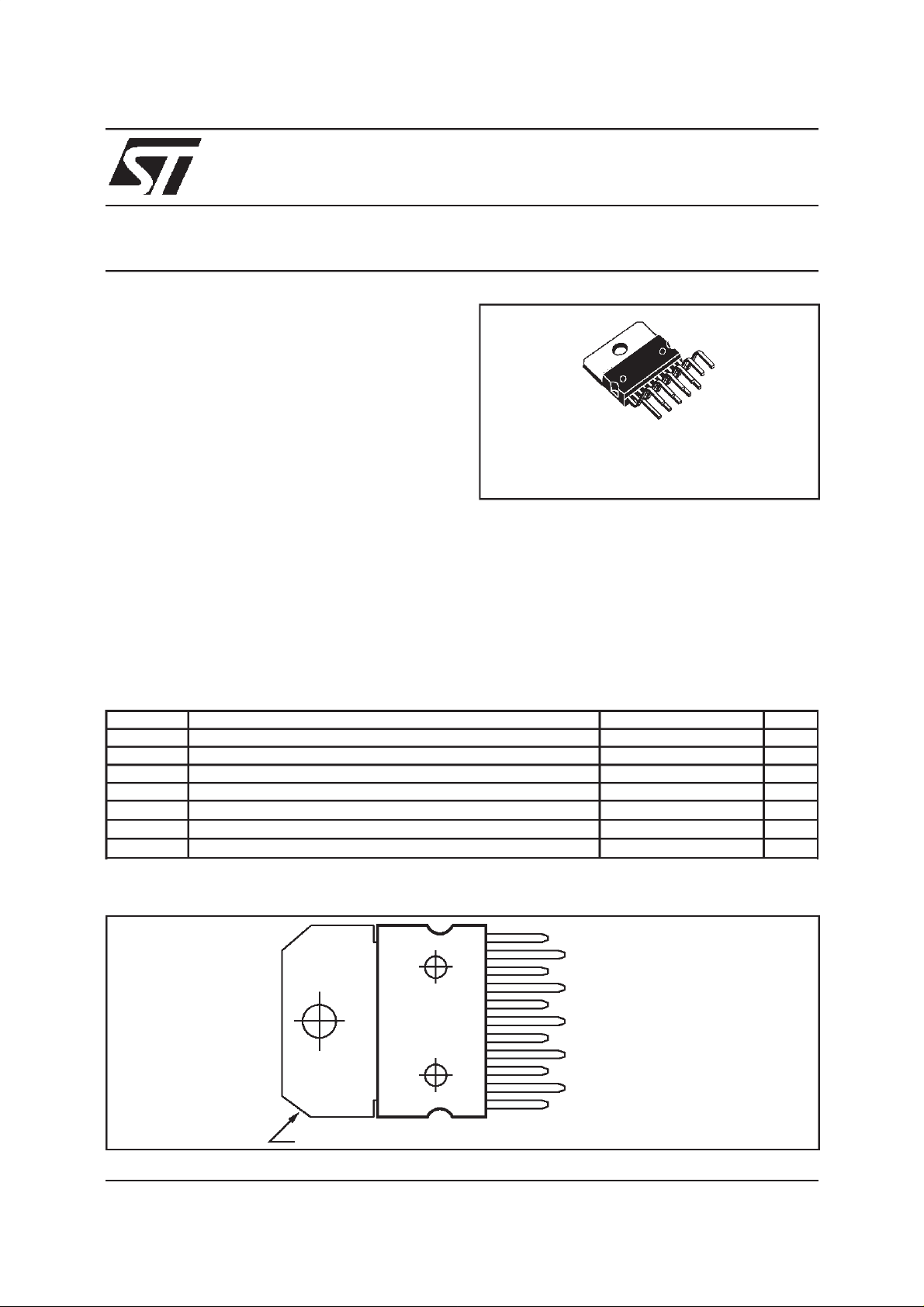
PIN CONNECTION
October 1998
TAB CONNECTEDTO PIN 6
11
10
9
8
7
6
5
4
3
2
1
D95AU318
BOOTSTRAP(1)
OUTPUT(1)
+V
S
OUTPUT(2)
BOOTSTRAP(2)
GND
INPUT+(2)
INPUT-(2)
SVRR
INPUT-(1)
INPUT+(1)
1/20
TDA2005
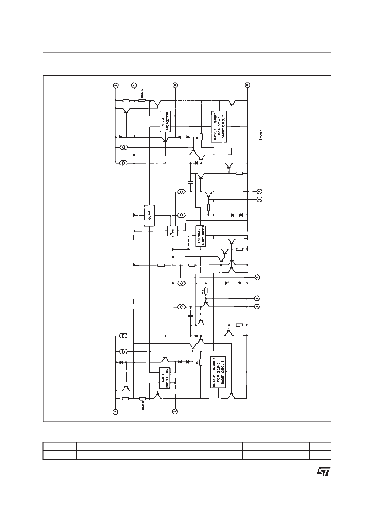
SCHEMATIC DIAGRAM
THERMALDATA
Symbol Parameter Value Unit
Thermal ResistanceJunction-case Max. 3 °
2/20
R
thj-case
C/W
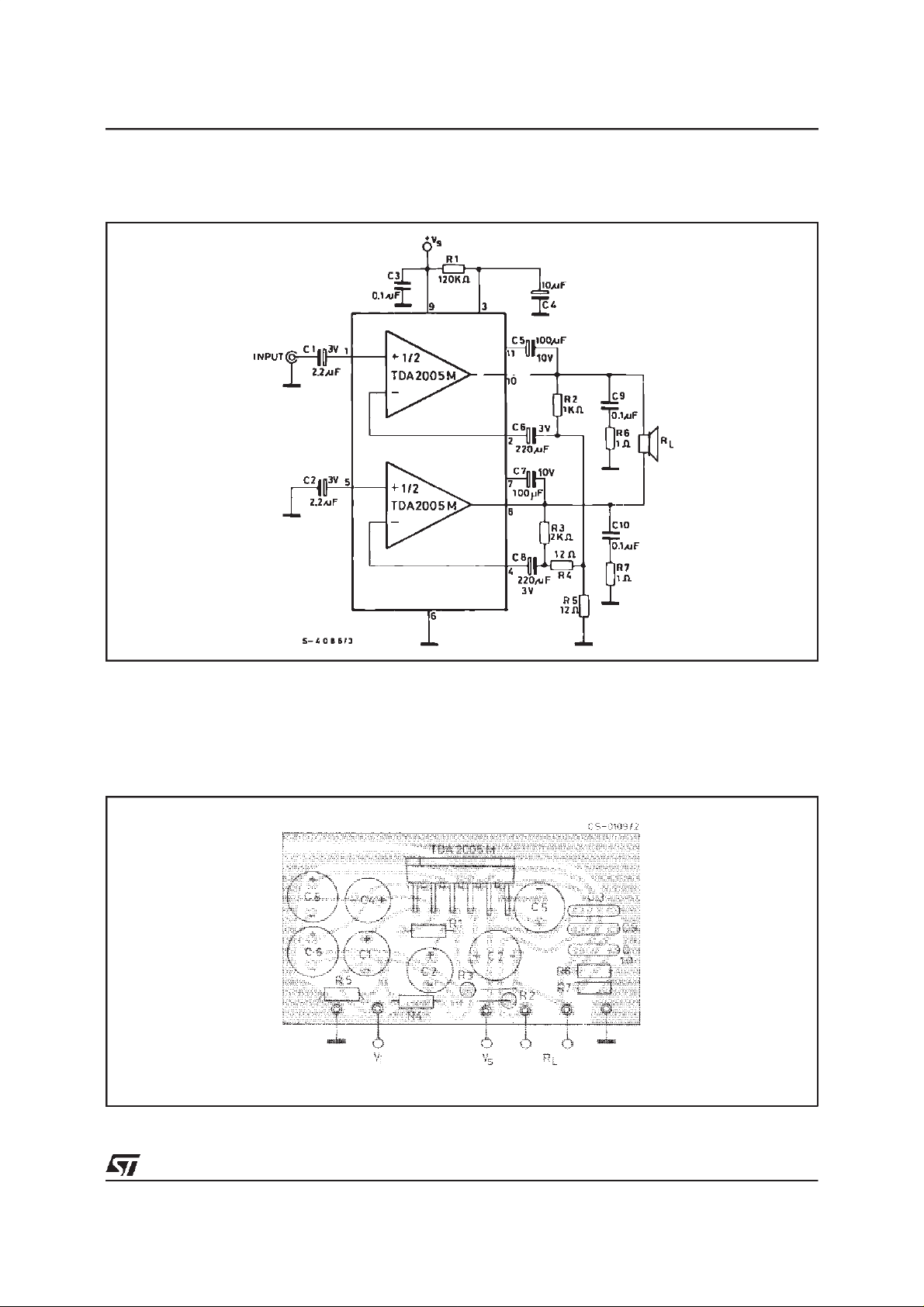
BRIDGE AMPLIFIERAPPLICATION(TDA2005M)
Figure1 : Test and ApplicationCircuit (Bridgeamplifier)
TDA2005
Figure2 :
P.C.Board and ComponentsLayoutof Figure1 (1:1scale)
3/20
TDA2005
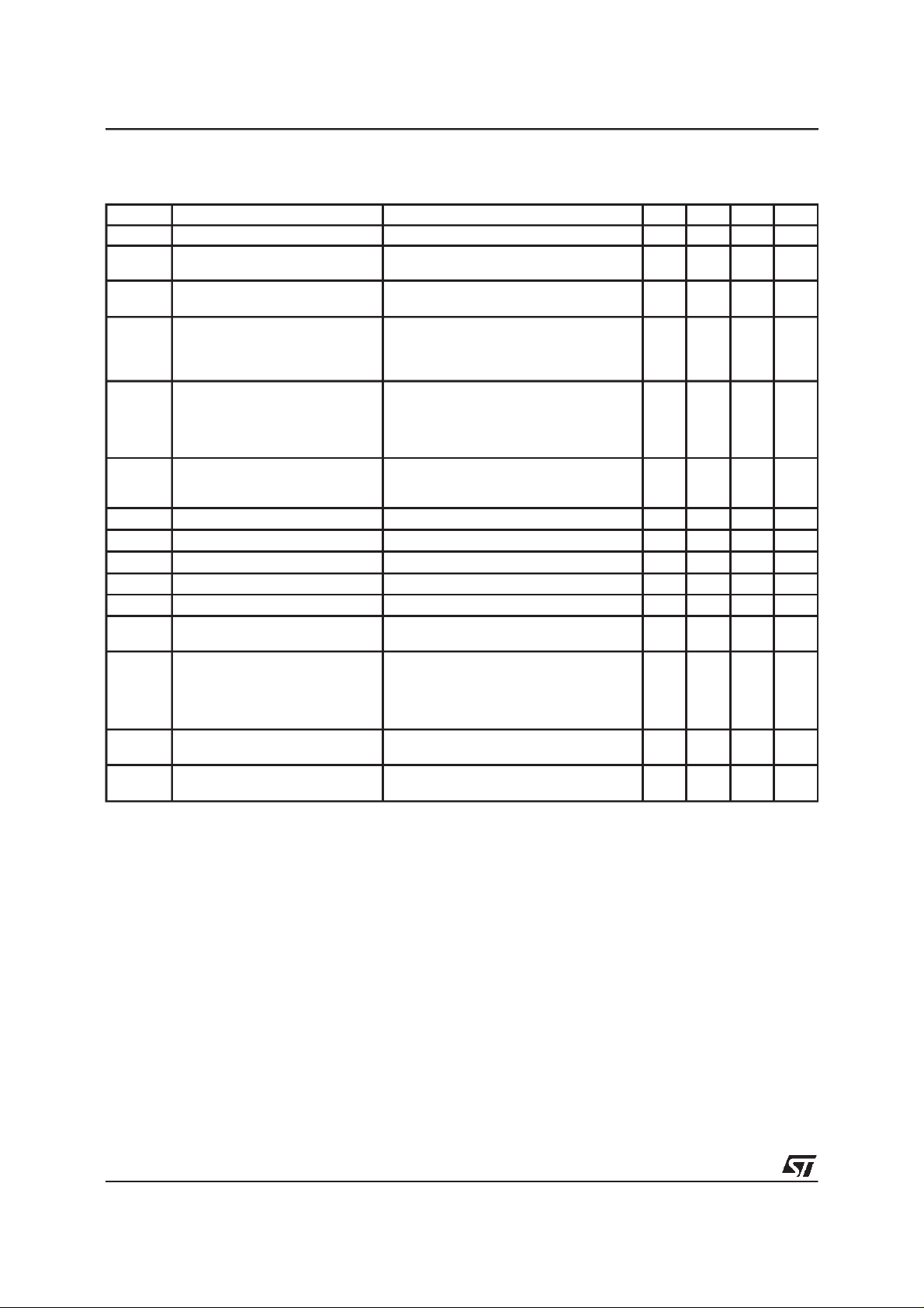
ELECTRICALCHARACTERISTICS
R
th (heatsink
)=4oC/W, unlessotherwise specified)
(referto the
Bridge
applicationcircuit, T
=25oC, GV=50dB,
amb
Symbol Parameter Test Conditions Min. Typ. Max. Unit
V
V
P
Supply Voltage 8 18 V
s
Output Offset Voltage (1)
os
(between pin 8 and pin 10)
Total Quiescent Drain Current
I
d
Output Power d = 10% f = 1 Hz
o
Vs= 14.4V
= 13.2V
V
s
= 14.4V RL=4Ω
V
s
V
= 13.2V RL= 3.2Ω
s
V
= 14.4V RL=4
s
V
= 13.2V RL= 3.2 Ω
s
R
L
= 3.2
Ω
18
Ω
20
17
150
150mVmV
7570150
160mAmA
20
22
19
d Distortion f = 1kHz
= 14.4V RL=4Ω
V
V
Input Sensitivity f = 1kHz
i
Input Resistance f = 1kHz 70
R
i
Low Frequency Roll Off (– 3dB)
f
L
High Frequency Roll Off (– 3dB)
f
H
G
e
Closed Loop Voltage Gain f = 1kHz 50 dB
v
Total Input Noise Voltage
N
SVR SupplyVoltage Rejection
Efficiency V
η
Thermal Shut-down Junction
T
j
Temperature
V
Notes :
Output Voltage with oneSide of
OSH
the Speaker shorted to ground
1. For TDA2005M only
2. Bandwith Filter :22Hz to 22kHz.
s
= 50mW to 15W
P
o
V
= 13.2V RL= 3.2
s
= 50mW to 13W
P
o
P
=2W RL=4Ω
o
P
=2W RL= 3.2Ω
o
= 3.2Ω
R
L
= 3.2
R
R
R
f
P
P
V
P
V
f = 1kHz, P
V
V
Ω 20 kHz
L
= 10kΩ(2)
g
= 10kΩ,C4=10µF
g
= 100Hz, V
ripple
= 14.4V, f = 1 kHz
s
= 20W RL=4Ω
o
= 22W RL= 3.2Ω
o
= 13.2V, f = 1 kHz
s
= 19W RL= 3.2Ω
o
= 14.4V, RL=4
s
= 14.4V RL=4Ω
s
= 13.2V RL= 3.2Ω
s
tot
ripple
Ω
= 13W
Ω
45 55 dB
= 0.5V
60
60
58
145
1
1
9
8
40 Hz
310µ
2V
W
%
%
mV
mV
k
Ω
V
%
%
%
C
°
4/20
TDA2005
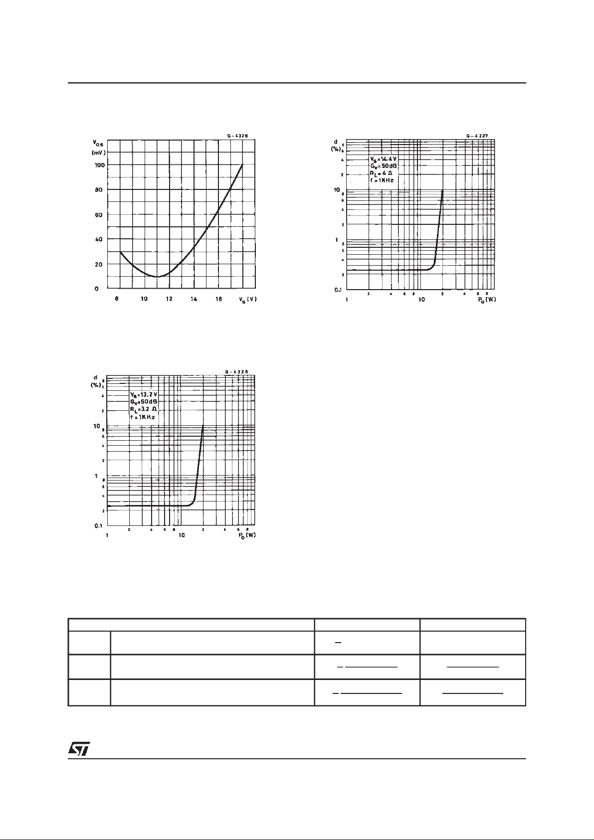
Figure3 : Output OffsetVoltage versus
SupplyVoltage
Figure5 :
Distortionversus Output Power
(bridgeamplifier)
Figure4 : Distortion versus Output Power
(bridgeamplifier)
BRIDGEAMPLIFIER DESIGN
The followingconsideraionscan be useful when designing a bridge amplifier.
Parameter Single Ended Bridge
1
V
omax
I
o max
P
omax
Where : V
Peak OutputVoltage (before clipping)
Peak OutputCurrent (before clippling)
RMS Output Power (before clipping)
= output transistors saturation voltage
CE sat
= allowablesupply voltage
V
S
= load impedance
R
L
(Vs–2V
2
V
1
S
2
(VS− 2V
1
4
− 2V
R
2R
CE sat
CE sat
L
CE sat
L
)
2
)
(V
V
V
S
–2V
s
− 2V
S
−2V
R
2R
CE sat
CE sat
L
CE sat
L
2
)
5/20
TDA2005
Voltageand current swings are twice for a bridge
amplifierincomparisonwith singleendedamplifier.
In order words, with the same R
the bridge con-
L
figuration can deliver an output power that is four
times theoutputpower of a singleended amplifier,
while,with the samemax output current thebridge
configuration can deliver an output power that is
twice the output powerof asingle ended amplifier.
Core must be taken when selecting V
and RLin
S
order to avoid an output peak current above the
absolute maximumrating.
From the expression for I
= 14.4V and V
= 2V, the minimum load that
CE sat
, assuming V
Omax
S
can be driven by TDA2005in bridgeconfiguration
is :
R
L min
− 2V
V
S
=
I
Omax
CEsat
=
14.4 −
3.5
4
=2.97Ω
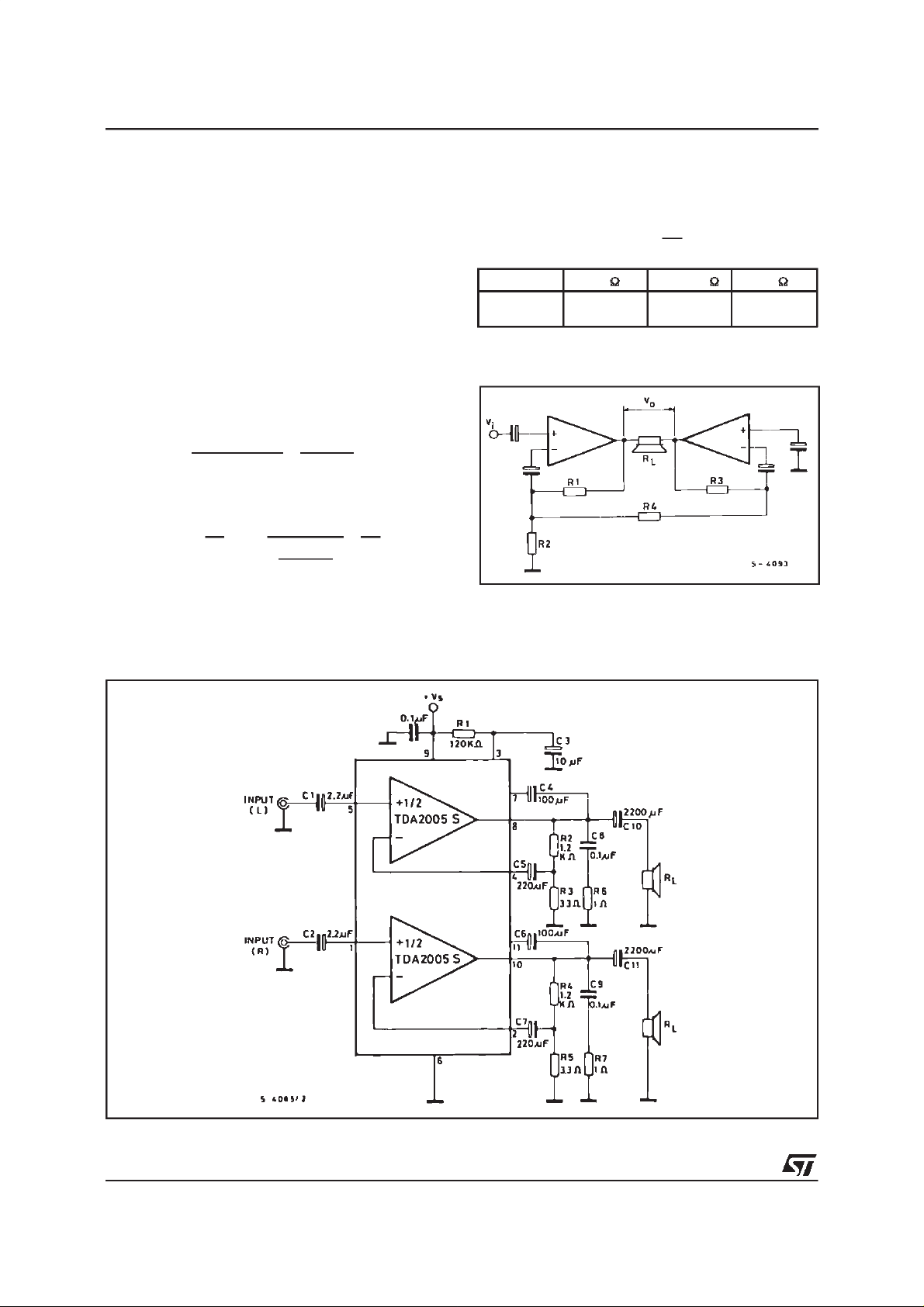
Thevoltagegainof thebridgeconfigurationisgiven
by (see Figure 34) :
V
0
=
V
=1+
1
G
V
R
R
2
R
1
2⋅R4
+R
R
3
+
R
4
4
STEREOAMPLIFIERAPPLICATION (TDA2005S)
Forsufficientlyhighgains(40 to50dB)itis possible
toput R
andR3=2R1, simplifingtheformula
2=R4
in :
R
1
=4
G
V
R
2
Gv(dB)
40
50
(Ω)R2=R4(Ω)R3(Ω)
R
1
1000
1000
39
12
2000
2000
Figure 6 : BridgeConfiguration
Figure7 :
TypicalApplicationCircuit
6/20

TDA2005
ELECTRICALCHARACTERISTICS
R
th (heatsink)
=4oC/W, unlessotherwwise specified
(referto the
Stereo
)
applicationcircuit, T
=25oC, GV=50dB,
amb
Symbol Parameter Test Conditions Min. Typ. Max. Unit
V
V
P
Supply Voltage 8 18 V
s
Quiescent Output Voltage Vs= 14.4V
o
Total Quiescent Drain Current Vs= 14.4V
I
d
Output Power (each channel) f = 1kHz, d = 10%
o
V
V
V
V
V
= 13.2V
s
= 13.2V
s
= 14.4V RL=4Ω
s
= 13.2V RL= 3.2Ω
s
= 16V RL=2Ω
s
R
R
R
R
L
L
L
L
= 3.2Ω
=2Ω
= 1.6Ω
= 1.6Ω
6.667.2
6
7
9
10
6
9
7.8
6.6
7.2VV
6562120
120mAmA
6.5
8
10
11
6.5
10
12
d Distortion (each channel) f = 1kHz
= 14.4V RL=4
CT Cross Talk (1) V
Input Saturation Voltage 300 mV
V
i
Input Sensitivity f = 1kHz, Po=1W
V
i
Input Resistance f = 1kHz 70 200
R
i
Low Frequency Roll Off (– 3dB)
f
L
High Frequency Roll Off (– 3dB)
f
H
G
G
∆ G
e
Voltage Gain (open loop) f = 1kHz 90 dB
v
Voltage Gain (closed loop) f = 1kHz 48 50 51 dB
v
Closed Loop Gain Matching 0.5 dB
v
Total Input Noise Voltage
N
SVR SupplyVoltage Rejection
Efficiency V
η
Notes : 1. For TDA2005Monly
2. Bandwith Filter :22Hz to 22kHz.
V
s
= 50mW to 4W
P
o
V
= 14.4V RL=2Ω
s
= 50mW to 6W
P
o
V
= 13.2V RL= 3.2Ω
s
= 50mW to 3W
P
o
= 13.2V RL= 1.6Ω
V
s
= 40mW to 6W
P
o
= 14.4V, Vo=4V
s
RL=4Ω,Rg=5k
=2Ω
R
L
=2
R
Ω
L
= 10kΩ (2)
R
g
= 10kΩ,C3=10µF
R
g
= 100Hz, V
f
ripple
= 14.4V, f= 1kHz
s
P
= 6.5W RL=4Ω
o
P
= 10W RL=2Ω
o
= 13.2V, f= 1kHz
V
s
P
= 6.5W RL= 3.2Ω
o
P
= 100W RL= 1.6Ω
o
RMS
Ω
f = 1kHz
f = 10kHz
R
=4Ω
L
R
= 3.2Ω
L
= 0.5V
ripple
Ω
0.2
0.3
0.2
0.3
1
1
1
1
60
45
6
5.5
50 Hz
15 kHz
1.5 5
35 45 dB
70
60
70
60
W
%
%
%
%
dB
mV
k
Ω
µV
%
%
%
%
7/20
 Loading...